JP5442479B2 - Indicator, position detection device and position detection method - Google Patents
Indicator, position detection device and position detection method Download PDFInfo
- Publication number
- JP5442479B2 JP5442479B2 JP2010024858A JP2010024858A JP5442479B2 JP 5442479 B2 JP5442479 B2 JP 5442479B2 JP 2010024858 A JP2010024858 A JP 2010024858A JP 2010024858 A JP2010024858 A JP 2010024858A JP 5442479 B2 JP5442479 B2 JP 5442479B2
- Authority
- JP
- Japan
- Prior art keywords
- code
- indicator
- codes
- correlation calculation
- circuit
- Prior art date
- Legal status (The legal status is an assumption and is not a legal conclusion. Google has not performed a legal analysis and makes no representation as to the accuracy of the status listed.)
- Active
Links
- 238000001514 detection method Methods 0.000 title claims description 132
- 239000004020 conductor Substances 0.000 claims description 176
- 238000004364 calculation method Methods 0.000 claims description 119
- 230000005540 biological transmission Effects 0.000 claims description 66
- 239000003990 capacitor Substances 0.000 claims description 33
- 238000000034 method Methods 0.000 claims description 23
- 230000008859 change Effects 0.000 claims description 18
- 230000007274 generation of a signal involved in cell-cell signaling Effects 0.000 claims description 17
- 230000008569 process Effects 0.000 claims description 15
- 230000005284 excitation Effects 0.000 claims description 8
- 238000010248 power generation Methods 0.000 claims description 8
- 230000004044 response Effects 0.000 claims description 8
- 230000007480 spreading Effects 0.000 description 41
- 238000003892 spreading Methods 0.000 description 41
- 230000004048 modification Effects 0.000 description 31
- 238000012986 modification Methods 0.000 description 31
- 238000006243 chemical reaction Methods 0.000 description 26
- 230000006870 function Effects 0.000 description 22
- 238000010586 diagram Methods 0.000 description 21
- 238000010168 coupling process Methods 0.000 description 9
- 230000002093 peripheral effect Effects 0.000 description 7
- 230000008878 coupling Effects 0.000 description 5
- 238000005859 coupling reaction Methods 0.000 description 5
- 238000004891 communication Methods 0.000 description 4
- 238000005516 engineering process Methods 0.000 description 4
- 230000008054 signal transmission Effects 0.000 description 3
- 239000000203 mixture Substances 0.000 description 2
- 238000003825 pressing Methods 0.000 description 2
- 239000007787 solid Substances 0.000 description 2
- 238000003860 storage Methods 0.000 description 2
- 230000007704 transition Effects 0.000 description 2
- RYGMFSIKBFXOCR-UHFFFAOYSA-N Copper Chemical compound [Cu] RYGMFSIKBFXOCR-UHFFFAOYSA-N 0.000 description 1
- 108010076504 Protein Sorting Signals Proteins 0.000 description 1
- 230000009471 action Effects 0.000 description 1
- 239000011889 copper foil Substances 0.000 description 1
- 230000003111 delayed effect Effects 0.000 description 1
- 238000007667 floating Methods 0.000 description 1
- 239000011521 glass Substances 0.000 description 1
- PCHJSUWPFVWCPO-UHFFFAOYSA-N gold Chemical compound [Au] PCHJSUWPFVWCPO-UHFFFAOYSA-N 0.000 description 1
- 239000010931 gold Substances 0.000 description 1
- 229910052737 gold Inorganic materials 0.000 description 1
- AMGQUBHHOARCQH-UHFFFAOYSA-N indium;oxotin Chemical compound [In].[Sn]=O AMGQUBHHOARCQH-UHFFFAOYSA-N 0.000 description 1
- 238000004519 manufacturing process Methods 0.000 description 1
- 239000000463 material Substances 0.000 description 1
- 239000002184 metal Substances 0.000 description 1
- 229910052751 metal Inorganic materials 0.000 description 1
- 230000010363 phase shift Effects 0.000 description 1
- 239000011295 pitch Substances 0.000 description 1
- 239000011347 resin Substances 0.000 description 1
- 229920005989 resin Polymers 0.000 description 1
- 230000035945 sensitivity Effects 0.000 description 1
- 125000006850 spacer group Chemical group 0.000 description 1
- 239000000758 substrate Substances 0.000 description 1
Images


Classifications
-
- G—PHYSICS
- G06—COMPUTING; CALCULATING OR COUNTING
- G06F—ELECTRIC DIGITAL DATA PROCESSING
- G06F3/00—Input arrangements for transferring data to be processed into a form capable of being handled by the computer; Output arrangements for transferring data from processing unit to output unit, e.g. interface arrangements
- G06F3/01—Input arrangements or combined input and output arrangements for interaction between user and computer
- G06F3/03—Arrangements for converting the position or the displacement of a member into a coded form
- G06F3/033—Pointing devices displaced or positioned by the user, e.g. mice, trackballs, pens or joysticks; Accessories therefor
- G06F3/0354—Pointing devices displaced or positioned by the user, e.g. mice, trackballs, pens or joysticks; Accessories therefor with detection of 2D relative movements between the device, or an operating part thereof, and a plane or surface, e.g. 2D mice, trackballs, pens or pucks
- G06F3/03545—Pens or stylus
-
- G—PHYSICS
- G06—COMPUTING; CALCULATING OR COUNTING
- G06F—ELECTRIC DIGITAL DATA PROCESSING
- G06F3/00—Input arrangements for transferring data to be processed into a form capable of being handled by the computer; Output arrangements for transferring data from processing unit to output unit, e.g. interface arrangements
- G06F3/01—Input arrangements or combined input and output arrangements for interaction between user and computer
- G06F3/03—Arrangements for converting the position or the displacement of a member into a coded form
- G06F3/033—Pointing devices displaced or positioned by the user, e.g. mice, trackballs, pens or joysticks; Accessories therefor
- G06F3/038—Control and interface arrangements therefor, e.g. drivers or device-embedded control circuitry
- G06F3/0383—Signal control means within the pointing device
-
- G—PHYSICS
- G06—COMPUTING; CALCULATING OR COUNTING
- G06F—ELECTRIC DIGITAL DATA PROCESSING
- G06F3/00—Input arrangements for transferring data to be processed into a form capable of being handled by the computer; Output arrangements for transferring data from processing unit to output unit, e.g. interface arrangements
- G06F3/01—Input arrangements or combined input and output arrangements for interaction between user and computer
- G06F3/03—Arrangements for converting the position or the displacement of a member into a coded form
- G06F3/041—Digitisers, e.g. for touch screens or touch pads, characterised by the transducing means
- G06F3/0416—Control or interface arrangements specially adapted for digitisers
- G06F3/04162—Control or interface arrangements specially adapted for digitisers for exchanging data with external devices, e.g. smart pens, via the digitiser sensing hardware
-
- G—PHYSICS
- G06—COMPUTING; CALCULATING OR COUNTING
- G06F—ELECTRIC DIGITAL DATA PROCESSING
- G06F3/00—Input arrangements for transferring data to be processed into a form capable of being handled by the computer; Output arrangements for transferring data from processing unit to output unit, e.g. interface arrangements
- G06F3/01—Input arrangements or combined input and output arrangements for interaction between user and computer
- G06F3/03—Arrangements for converting the position or the displacement of a member into a coded form
- G06F3/041—Digitisers, e.g. for touch screens or touch pads, characterised by the transducing means
- G06F3/044—Digitisers, e.g. for touch screens or touch pads, characterised by the transducing means by capacitive means
- G06F3/0442—Digitisers, e.g. for touch screens or touch pads, characterised by the transducing means by capacitive means using active external devices, e.g. active pens, for transmitting changes in electrical potential to be received by the digitiser
-
- G—PHYSICS
- G06—COMPUTING; CALCULATING OR COUNTING
- G06F—ELECTRIC DIGITAL DATA PROCESSING
- G06F3/00—Input arrangements for transferring data to be processed into a form capable of being handled by the computer; Output arrangements for transferring data from processing unit to output unit, e.g. interface arrangements
- G06F3/01—Input arrangements or combined input and output arrangements for interaction between user and computer
- G06F3/03—Arrangements for converting the position or the displacement of a member into a coded form
- G06F3/041—Digitisers, e.g. for touch screens or touch pads, characterised by the transducing means
- G06F3/044—Digitisers, e.g. for touch screens or touch pads, characterised by the transducing means by capacitive means
- G06F3/0446—Digitisers, e.g. for touch screens or touch pads, characterised by the transducing means by capacitive means using a grid-like structure of electrodes in at least two directions, e.g. using row and column electrodes
-
- G—PHYSICS
- G06—COMPUTING; CALCULATING OR COUNTING
- G06F—ELECTRIC DIGITAL DATA PROCESSING
- G06F3/00—Input arrangements for transferring data to be processed into a form capable of being handled by the computer; Output arrangements for transferring data from processing unit to output unit, e.g. interface arrangements
- G06F3/01—Input arrangements or combined input and output arrangements for interaction between user and computer
- G06F3/03—Arrangements for converting the position or the displacement of a member into a coded form
- G06F3/041—Digitisers, e.g. for touch screens or touch pads, characterised by the transducing means
- G06F3/046—Digitisers, e.g. for touch screens or touch pads, characterised by the transducing means by electromagnetic means
Description
本発明は指示体、位置検出装置及び位置検出方法に関し、より詳細には、静電結合方式における指示体、位置検出装置及び位置検出方法に関する。 The present invention relates to an indicator, a position detection device, and a position detection method, and more particularly to an indicator, a position detection device, and a position detection method in an electrostatic coupling method.
従来、コンピュータ装置上で描画やイラスト作成などに用いられるポインティングデバイスの一つとして、タブレットと呼ばれる位置検出装置が開発されている。このような位置検出装置は、通常、略平板状の位置検出器と、ユーザが位置検出器上で操作するペン形状の指示体とで構成される。 2. Description of the Related Art Conventionally, a position detection device called a tablet has been developed as one of pointing devices used for drawing and illustration creation on a computer device. Such a position detection device is generally composed of a substantially flat position detector and a pen-shaped indicator operated by the user on the position detector.
上述のような位置検出装置において、従来、静電結合方式を採用した位置検出装置が提案されている。静電結合方式の位置検出装置は、主に、集積回路(IC:Integrated Circuit)を含む指示体と、所定パターンで配列された導体群を有するセンサ部を備える位置検出器とで構成される。そして、センサ部上の指示体から導体群に所定の信号を送信し、位置検出器でその送信信号の受信位置を特定することにより指示体の指示位置を検出する。 Conventionally, position detection devices employing the electrostatic coupling method have been proposed for the position detection devices as described above. The electrostatic coupling type position detection device mainly includes an indicator including an integrated circuit (IC) and a position detector including a sensor unit having conductor groups arranged in a predetermined pattern. A predetermined signal is transmitted from the indicator on the sensor unit to the conductor group, and the position of the indicator is detected by specifying the reception position of the transmission signal with the position detector.
静電結合方式の位置検出装置において、通常、指示体からセンサ部に送信される信号は指示体が指示する位置を検出するために用いられる。それゆえ、このような位置検出装置では、指示体が指示する位置の検出は可能であるが、例えば指示体の筆圧情報、指示体が位置検出器にコンタクトしたことを示すペンダウン情報等の、位置情報以外の情報を検出することができないという課題があった。更には、ペン形状の指示体と指示体としての指など、複数種類の指示体を同時に検出できないという課題もあった。 In the electrostatic coupling type position detection device, a signal transmitted from the indicator to the sensor unit is usually used to detect a position indicated by the indicator. Therefore, in such a position detection device, it is possible to detect the position indicated by the indicator, for example, pen pressure information of the indicator, pen down information indicating that the indicator has contacted the position detector, etc. There was a problem that information other than position information could not be detected. Furthermore, there is a problem that plural types of indicators such as a pen-shaped indicator and a finger as an indicator cannot be detected at the same time.
本発明は、上記課題を解決するためになされたものである。本発明の目的は、静電結合方式を採用した位置検出装置において、相関演算処理が行われる符号を用いることで、指示体が指示する位置だけでなく、例えば筆圧情報、あるいは指示体のペンチップを回転の中心点として指示体を位置検出器上で回転させた場合のその回転位置、あるいは傾きなど、位置情報以外の情報を検出可能とすることである。更には、指示体としての指による位置指示情報など、複数種類の指示体による情報をも同時に検出可能とする。 The present invention has been made to solve the above problems. An object of the present invention is to use not only the position indicated by the indicator but also, for example, the pen pressure information or the pen tip of the indicator by using a code for which correlation calculation processing is performed in the position detection device adopting the electrostatic coupling method. It is possible to detect information other than position information, such as the rotation position or inclination when the indicator is rotated on the position detector with the rotation center as the rotation point. Furthermore, information by a plurality of types of indicators such as position indication information by a finger as an indicator can be detected simultaneously.
上記問題を解決するために、本発明の位置検出装置は、指示体に印加された圧力を2つの符号間の時間差に対応づけて送信するための送信信号生成部を備え前記送信信号生成部によって生成された信号を送信するための指示体と、所定方向に配置された複数の第1の導体と前記所定方向と交差する方向に配置された複数の第2の導体を備え前記指示体から送信された信号を受信するためのセンサ部と、前記複数の第1の導体を構成する導体と前記複数の第2の導体を構成する導体にそれぞれ生起した信号と前記2つの符号に対応した相関演算用符号との相関演算を行うための相関演算回路と、前記相関演算回路によって算出された少なくとも1つの符号に基づく相関演算結果から前記指示体によって指示されたセンサ部上の位置を検出するための位置算出回路と、前記相関演算回路によって算出された2つの符号に基づく相関演算結果から前記2つの符号間の時間差に対応して前記指示体に印加された圧力を検出する筆圧算出回路と、を備える。また、指示体のペンチップを回転の中心点として指示体を位置検出器上で回転させた場合のその回転位置、あるいは傾きなど、位置情報以外の情報を検出可能とするために、指示体にはその中心軸の周囲に電気的に分割された複数の電極片が配置され、それぞれの電極片に、種類の異なる符号を供給する。更には、指による指示操作をも同時検出可能とするために、位置検出器内に符号生成部とセンサ部を構成する導体を信号受信用と信号送信用に切り替えるための切替部を備える。 In order to solve the above problem, the position detection device of the present invention includes a transmission signal generation unit for transmitting the pressure applied to the indicator in association with the time difference between the two codes, by the transmission signal generation unit. An indicator for transmitting the generated signal, a plurality of first conductors arranged in a predetermined direction, and a plurality of second conductors arranged in a direction intersecting the predetermined direction are transmitted from the indicator Sensor unit for receiving the generated signals, signals generated in the conductors constituting the plurality of first conductors and the conductors constituting the plurality of second conductors, and correlation calculation corresponding to the two codes A correlation calculation circuit for performing a correlation calculation with a code for use, and a position on the sensor unit indicated by the indicator from a correlation calculation result based on at least one code calculated by the correlation calculation circuit And a writing pressure calculation circuit for detecting a pressure applied to the indicator corresponding to a time difference between the two codes from a correlation calculation result based on the two codes calculated by the correlation calculation circuit; . In addition, in order to be able to detect information other than position information such as the rotation position or inclination when the indicator is rotated on the position detector with the pen tip of the indicator as the center point of rotation, A plurality of electrically divided electrode pieces are arranged around the central axis, and different types of codes are supplied to the respective electrode pieces. Furthermore, in order to be able to simultaneously detect an instruction operation with a finger, the position detector includes a switching unit for switching the conductors constituting the code generation unit and the sensor unit for signal reception and signal transmission.
なお、上記2つの符号は、符号パターンが同一の符号であっても良いし、互いに異なる符号パターンを用いることもできる。なお、同一の符号パターンを使用する場合には、この符号パターンに対応した同一の相関演算用符号を使用することができる。 The two codes may have the same code pattern, or different code patterns may be used. When the same code pattern is used, the same correlation calculation code corresponding to this code pattern can be used.
また、本発明の指示体は、位置を指示するための先端部(ペンチップ)が筐体から突出して備えられた指示体であって、符号パターンが互いに異なる第1の符号及び第2の符号が生成されるとともに前記指示体の先端部に印加された圧力を、相関演算により識別可能なパターンを有する2つの符号が生成されるタイミングすなわち符号間の時間差(位相差)を制御し、あるいは所定の符号パターンを有する1つの符号が生成されるとともに前記指示体の先端部に印加された圧力に対応して、斯かる符号の最初の生成に対する次の生成のタイミングすなわち符号間の時間差(位相差)を制御する符号生成回路と、前記符号生成回路によって生成された符号を送信するための送信信号生成部と、を備える。 The indicator of the present invention is an indicator provided with a tip portion (pen tip) for instructing a position so as to protrude from the housing, and the first code and the second code having different code patterns are provided. The pressure generated and applied to the tip of the indicator is controlled by controlling the timing at which two codes having a pattern that can be identified by correlation calculation, that is, the time difference (phase difference) between the codes, One code having a code pattern is generated and corresponding to the pressure applied to the tip of the indicator, the timing of the next generation relative to the first generation of the code, ie the time difference (phase difference) between the codes And a transmission signal generation unit for transmitting the code generated by the code generation circuit.
本発明は、位置検出装置に静電結合方式を採用した場合に好適な発明であり、指示体から時間差を有して送信された、同一の符号パターンを有する、あるいは符号パターンが互いに異なる、第1及び第2の符号を受信し、第1の符号を用いて指示体の位置検出を行い、更には、第2の符号との間の時間差に基づいて、例えば筆圧情報、あるいは指示体の回転位置情報などの位置情報以外の情報を得る。 The present invention is suitable for the case where the electrostatic coupling method is adopted for the position detection device, and is transmitted with a time difference from the indicator, has the same code pattern, or has different code patterns. The first and second codes are received, the position of the indicator is detected using the first code, and furthermore, based on the time difference from the second code, for example, the pen pressure information or the indicator Information other than position information such as rotational position information is obtained.
上述のように、本発明では、指示体から、互いの符号パターンが同一、あるいは異なる、第1の符号および第2の符号を送信し、信号受信時には受信信号と、第1および第2の符号に対応したそれぞれの相関演算用符号との間の相関演算を行うことで、指示体の指示位置だけでなく、例えば筆圧情報等の位置情報以外の情報を検出することができる。 As described above, in the present invention, the first code and the second code having the same or different code patterns are transmitted from the indicator, and the received signal and the first and second codes are received at the time of signal reception. By performing a correlation calculation with each correlation calculation code corresponding to, information other than position information such as writing pressure information can be detected in addition to the pointing position of the pointer.
以下、本発明の位置検出装置の一実施形態を、図面を参照しながら具体的に説明する。ただし、本発明は下記実施形態に限定されるものではない。 Hereinafter, an embodiment of the position detection device of the present invention will be specifically described with reference to the drawings. However, the present invention is not limited to the following embodiment.
本実施形態では、互いに符号パターンが異なる2つの符号、あるいは互いが同一の符号パターンを有する2つの符号を用いて指示体の位置及び筆圧、すなわち指示体に印加した圧力を検出する。使用する符号としては、例えば8ビットコードであれば、「11110000」、「11001100」、及び「10101010」の中から必要に応じて1つあるいは複数の符号パターンを使用する。また、「00101101」、「11001100」、及び「10101010」の符号パターンも使用し得る。 In the present embodiment, the position and writing pressure of the indicator, that is, the pressure applied to the indicator, is detected using two codes having different code patterns or two codes having the same code pattern. For example, in the case of an 8-bit code, one or a plurality of code patterns are used from among “11110000”, “11001100”, and “10101010” as necessary. Also, code patterns “00101101”, “11001100”, and “10101010” may be used.
これらの符号パターンを使用すれば、受信時の相関演算処理によって互いの符号パターンを識別できる。他の符号としては、例えばM系列、ゴールド符号系列等を含む拡散符号や、例えばアダマール符号、ウォルシュ符号等の直交符号を用いてもよい。なお、直交符号を用いることで、受信時の相関演算処理によって互いの符号パターンの識別感度を高めることができる。 If these code patterns are used, the code patterns can be identified by the correlation calculation process at the time of reception. As other codes, for example, spreading codes including M series, Gold code series, etc., and orthogonal codes such as Hadamard code and Walsh code may be used. In addition, by using orthogonal codes, the identification sensitivity of each code pattern can be increased by the correlation calculation process at the time of reception.
[位置検出装置の構成]
図1に、本実施形態の位置検出装置の外観斜視図を示す。なお、本実施形態では、位置検出装置としてタブレットを用いた例を説明する。位置検出装置1は、ペン形状の指示体2と、平板形状の位置検出器3とで構成され、外部機器接続ケーブル4を介してパーソナルコンピュータ(PC)などの外部機器に接続される。
[Configuration of position detection device]
FIG. 1 shows an external perspective view of the position detection device of the present embodiment. In the present embodiment, an example in which a tablet is used as the position detection device will be described. The
指示体2は、位置検出器3のスキャン可能領域3a上で使用する。このスキャン可能領域3a上では、位置検出器3により指示体2の指示位置(座標)や筆圧などが検出できるようになっている。
The
位置検出器3は、指示体2が指示した位置の座標を検出し、その座標情報を外部機器に出力する。そして、外部機器の表示画面(不図示)上では、位置検出器3から入力された座標情報に対応する位置にポインタ等が表示される。
The
[指示体の構成]
図2に、本実施形態の指示体2の概略構成を示す。指示体2は、第1電極20と、第2電極21と、可変容量コンデンサ22と、集積回路23と、コイル24と、電源生成回路25と、これらの構成部材を内包する筐体129とを備える。可変容量コンデンサ22は、印加される圧力に応じて容量値を変化させるコンデンサである。筐体129は金属などの導電性を有する材質で構成される。
[Composition of indicator]
In FIG. 2, schematic structure of the
第1電極20は、棒形状を有しており、その一方の先端部は筐体129の一方の端部から突き出るように配置される。また、その先端部は、導電性を備えることでペンチップとして機能する。すなわち、筐体129から突き出た先端部は、指示体2のペンチップとして機能すると共に第1電極20としても機能する。一方、第2電極21は、この例では略円筒状の電極であり、第1電極20を取り囲むように配置される。すなわち、棒形状の第1電極20を中心として筐体129の内周面に沿って配置される。また、集積回路23から出力される符号(C1、C2)は、抵抗(R1、R2)を介して信号加算された後、第1電極20及び第2電極21に供給される。従って、集積回路23から出力された2つの符号パターンにそれぞれ対応した信号が信号加算された形態で第1電極20及び第2電極21に印加されることにより、第1電極20及び第2電極21を介して位置検出器3に信号が送信される。
The
圧力検出素子として配置された可変容量コンデンサ22は、ペンチップに加えられた圧力、いわゆる筆圧により容量が変化する構成を備える。具体的には、可変容量コンデンサ22を構成する一対の電極(不図示)のうち一方の電極が、第1電極20の端部と係合するように構成される。それゆえ、指示体2を位置検出器3に接触させて第1電極20がスキャン可能領域3a上で押されると、可変容量コンデンサ22の一方の電極も押圧される。これにより可変容量コンデンサ22の一対の電極間の電気的特性が変化することで、コンデンサの容量が変化する。すなわち、可変容量コンデンサ22の容量変化量は筆圧と対応することになる。なお、圧力検出素子としては、筆圧に応じてインダクタンスが変化するように構成されたインダクタンス可変コイルまたは筆圧に応じて抵抗値が変化するように構成された可変抵抗を用いてもよい。また、可変容量コンデンサ、インダクタンス可変コイル及び可変抵抗のいずれかを含む共振回路を用いてもよい。要は、圧力検出素子は、指示体2の先端部(ペンチップ)に印加された圧力(筆圧)が送信符号生成部28から出力される符号信号の生成開始タイミング(位相)に作用する構成を備えていればよい。
The
第1符号生成部26及び第2符号生成部27を含む送信符号生成部28は、集積回路23を構成する。本実施形態では、第1符号生成部26から出力される第1符号C1を用いて位置検出を行い、更には第2符号生成部27から出力される第2符号C2をも用いて筆圧検出を行う。
The transmission
また、集積回路23の各出力端子は、抵抗(R1、R2)を介して第1電極20及び第2電極21にそれぞれ接続されており、所定のタイミングで第1符号C1及び/又は第2符号C2に対応した送信信号を第1電極20及び第2電極21に出力する。なお、本実施形態では、第1符号生成部26から出力される第1符号C1と、第2符号生成部27から出力される第2符号C2とは、符号パターンが互いに異なるものとする。ただし、本発明はこれに限定されず、後述するように、同じ符号パターンを使用し、互いの符号間の信号生成開始タイミング(位相)を制御することにより、2つの符号を生成してもよい。
In addition, each output terminal of the
第2符号生成部27は、可変容量コンデンサ22に接続される。そして、第2符号生成部27は、筆圧に対応した可変容量コンデンサ22の容量変化に基づいて、第2符号C2の信号生成開始タイミング(位相)を変化させる。すなわち、本実施形態では、第1符号生成部26から出力される第1符号C1の生成タイミングと、第2符号C2の生成タイミングとの間の時間差(位相差)が、指示体2に印加された筆圧に対応するように構成される。
The second
さらに、集積回路23は、送信符号生成部28の動作を制御する制御回路(不図示)を備え、その制御に必要なクロック信号等は制御回路により生成される。なお、集積回路23は、後述するコイル24及び電源生成回路25により生成される電圧により駆動される。
Furthermore, the
コイル24は、位置検出器3に備えられた、後述のセンサ部30の励磁コイル35から送出される励磁信号を受信する。これにより、コイル24に高周波信号が誘起される。そして、この誘起された高周波信号は、電源生成回路25に入力される。電源生成回路25は、整流回路(不図示)を有し、コイル24から供給された高周波信号を、整流回路により、整流して直流電圧に変換する。そして、電源生成回路25は、変換された直流電圧を集積回路23の駆動用電源として集積回路23に供給する。
The
なお、本実施形態では、集積回路23内に第1符号C1及び第2符号C2をそれぞれ生成する第1符号生成部26及び第2符号生成部27を設ける例を説明したが、本発明はこれに限定されない。集積回路23内に例えばROM(Read Only Memory)を設け、このROMに予め第1符号C1及び第2符号C2を記憶しておき、符号送信時にこのROMからこれらの符号パターンを読み出して送信する構成にしてもよい。なお、この場合、可変容量コンデンサ22の容量変化量ΔCと、第1符号C1の信号生成開始タイミングと第2符号C2の信号生成開始タイミングとの対応関係を予めテーブル化してROMに記憶しておく。
In this embodiment, the example in which the first
図3(a)及び(b)は、図2に示す指示体2内の送信符号生成部28の回路構成例を示す。図3(a)は、第1符号C1及び第2符号C2の符号パターンが互いに異なる場合の送信符号生成部28の回路構成例である。第1電極20を介して印加される圧力に応じて容量が変化する可変容量コンデンサ22の一端は、グラウンドに接続される。その他端は、抵抗144を介して電源生成回路25に接続されて所定の電圧Vccが供給される。
FIGS. 3A and 3B show circuit configuration examples of the transmission
タイミング制御回路141は、所定の周期t1でスイッチ143のON/OFF制御を行う。すなわち、スイッチ143は、タイミング制御回路141により、一旦ONとされて可変容量コンデンサ22の電荷を放電し、その後、OFFとされる。また、タイミング制御回路141は、スイッチ143をOFFにするとともに、第1符号生成部26に作用して第1符号C1の生成を指示する。スイッチ143がOFFされると、可変容量コンデンサ22は抵抗144を介して次第に充電される。この際、可変容量コンデンサ22の両端での電位は、筆圧に対応して変化した容量値に依存して、次第に上昇する。
The
遅延設定回路142は、タイミング制御回路141からの制御信号の供給に対応して、可変容量コンデンサ22の電位と所定の電位Vthとの比較を行う。可変容量コンデンサ22の電位が所定の電位Vthに達すると第2符号生成部27に作用して第2符号C2の生成を指示する。この構成により、ペンチップに印加された筆圧に対応して変化した容量値に基づいて、第1符号生成部26による第1符号C1の符号生成タイミングと第2符号生成部27による第2符号C2の符号生成タイミングとの間の差、すなわち第1符号C1と第2符号C2との間の位相が変化することになる。この位相変化を検出することで筆圧が検出可能となる。
In response to the supply of the control signal from the
図3(b)は、第1符号C1及び第2符号C2に同じ符号パターンを使用する場合の送信符号生成部28の回路構成例である。すなわち、1種類の符号を使用する場合の回路構成例を示す。この例では、図3(a)における第2符号生成部27に代えて、第1符号生成部26を使用するものであり、それ以外の構成は同一である。この例のように第1符号C1と第2符号C2が同一の符号パターンであっても、両者の間の位相は筆圧に応じて変化するので、この位相変化を検出することで筆圧が検出可能となる。
FIG. 3B is a circuit configuration example of the transmission
[位置検出器の構成]
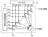
図4に、位置検出器3の概略構成を示す。位置検出器3は、主に、指示体2の指示位置を検出するためのセンサ部30と、センサ部30を構成する複数の導体を選択する選択回路40と、位置検出回路50とで構成される。なお、図4では、受信信号の処理の流れを実線矢印で示し、制御信号、クロック信号等の流れは破線矢印で示す。ただし、図4では、説明を簡略化するため、受信系回路群51の制御信号、クロック信号等の流れを示す破線矢印は省略する。
[Configuration of position detector]
FIG. 4 shows a schematic configuration of the
センサ部30は、図4中のx方向(所定方向)に延在した複数の第1導体31からなる第1導体群32と、第1導体31の延在方向と交差する方向、すなわち、図4中のy方向に延在した複数の第2導体33からなる第2導体群34と、それらの導体群の周囲に設けられた励磁コイル35とを備える。第1導体群32を構成する複数の第1導体31は、所定間隔で図4中のy方向に並列配置される。一方、第2導体群34を構成する複数の第2導体33は、所定間隔で図4中のx方向に並列配置される。
The sensor unit 30 includes a
なお、第1導体31及び第2導体33は、例えば、ITO(Indium Tin Oxide)膜からなる透明電極膜や、銅箔等で形成される。また、第1導体群32及び第2導体群34は、樹脂材料等からなるスペーサやガラス基板等(不図示)を介して積層される。また、第1導体群32及び第2導体群34の各導体は、選択回路40に接続される。励磁コイル35は、位置検出回路50内の後述するドライブ回路61に接続される。
The
第1導体31及び第2導体33の本数及びピッチは、センサ部30のサイズや必要とする検出精度等に応じて適宜設定される。また、本実施形態では、第1導体31及び第2導体33として直線状の導体を例示しているが、本発明はこれに限定されない。例えば、第1導体31及び第2導体33がともに延在方向に対して交差する方向に蛇行していてもよい。また、例えば、第1導体31及び第2導体33の一方をリング状の導体で構成し、他方をリング状導体の中心から半径方向に延在する導体で構成してもよい。
The numbers and pitches of the
選択回路40は、第1導体群32及び第2導体群34から所定の導体を、例えば順次選択するなど、所定の順序で選択する。この選択回路40による導体選択制御は、後述する中央演算処理部62と協働する制御部63から出力される制御信号(図4中の破線矢印)により制御される。なお、この実施態様においては、センサ部30は少なくとも指示体2から送信された所定の信号を受信する構成を備えるものである。また、本実施形態は、受信系回路群51を時分割動作させるために、選択回路40によって第1導体群32及び第2導体群34から、それぞれ所定の導体を選択することで指示体2が指示する位置(X座標、Y座標)を検出する構成を備える。なお、センサ部30を構成する導体の数に対応した複数の受信系回路群51を備える構成を採用すれば、選択回路40を省略することができることは明らかである。
The selection circuit 40 selects a predetermined conductor from the
位置検出回路50は、受信系回路群51と、発振器60と、ドライブ回路61と、中央演算処理部62(CPU:Central Processing Unit)と、制御部63とを備える。
The position detection circuit 50 includes a reception
発振器60は、所定周波数の交流信号又はパルス信号をドライブ回路61に出力する。ドライブ回路61は、発振器60から入力された信号を電流に変換して励磁コイル35に出力する。
The
制御部63は、中央演算処理部62と協働して、位置検出回路50内の各部に制御信号(図4中の破線矢印)を出力するとともに、受信系回路群51内の後述する位置及び筆圧算出部58の算出結果を外部機器に出力する。また、中央演算処理部62は、ソフトウェアプログラムを含み、制御部63の動作を制御する。
The
受信系回路群51は、主に、受信アンプ52と、A/D(Analog to Digital)変換回路53と、シリアルパラレル変換部54と、シフトレジスタ55と、相関演算部56と、メモリ57と、位置及び筆圧算出部58(検出部)とで構成される。そして、受信アンプ52、A/D変換回路53、シリアルパラレル変換部54、シフトレジスタ55、相関演算部56、メモリ57、並びに、位置及び筆圧算出部58は、選択回路40側からこの順で接続される。
The reception
受信アンプ52は、選択回路40で選択された所定の導体から入力される受信信号を増幅する。そして、受信アンプ52は、この増幅された受信信号をA/D変換回路53に出力する。A/D変換回路53は、増幅された受信信号をアナログデジタル変換して、変換したデジタル信号をシリアルパラレル変換部54に出力する。
The
シリアルパラレル変換部54は、例えば、直列入力並列出力型のシフトレジスタで構成されており、使用する符号の符号長に対応した段数のフリップフロップを有する。シリアルパラレル変換部54は、実行プログラムが収納された中央演算処理部62と協働する、制御部63によってその動作が制御される。なお、シリアルパラレル変換部54を構成する各段のフリップフロップは、1ビットの情報を保持できるフリップフロップを用いてもよいし、マルチビット(例えば10ビット等)の情報を保持できるフリップフロップを用いてもよい。
The serial /
シリアルパラレル変換部54を構成する各段のフリップフロップは、入力された受信信号を順次次段のフリップフロップにシフトする。また、各フリップフロップの出力端子は、多段フリップフロップで構成される後述のシフトレジスタ55内の対応するフリップフロップの入力端子に接続される。その結果、シリアルパラレル変換部54からは、使用する符号の符号長と同じ数の出力信号がシフトレジスタ55にパラレル出力される。
The flip-flops at each stage constituting the serial /
シフトレジスタ55は、並列入出力型のシフトレジスタであり、使用する符号の符号長と同じ段数のフリップフロップにて構成される。なお、シフトレジスタ55を構成する各段のフリップフロップには、1ビットの情報を保持できるフリップフロップを用いてもよいし、マルチビット(例えば10ビット等)の情報を保持できるフリップフロップを用いてもよい。
The
シフトレジスタ55内の各フリップフロップは、中央演算処理部62と協働する制御部63によってその動作が制御される。また、シフトレジスタ55を構成する各フリップフロップは、入力された信号を次段のフリップフロップに巡回的にシフトさせるとともに、その信号を後述する相関演算部56内の対応する積算器56dに出力する。
The operation of each flip-flop in the
なお、シリアルパラレル変換部54とシフトレジスタ55との間にシリアルパラレル変換部54から出力される信号を一時的に保持するバッファとして機能するレジスタを設けてもよい。この場合には、シフトレジスタ55に保持された受信信号を巡回させながら相関値を演算する間に、次の相関値演算に必要な信号をそのレジスタに一時的に保持させることができる。
A register that functions as a buffer that temporarily holds a signal output from the serial /
相関演算部56は、シフトレジスタ55から出力された受信信号と、所定の符号パターンを有する符号(以下、相関演算用符号という)との相関値を演算して、受信信号の相関特性を出力する。
The
図5に、指示体2から送信される符号として、互いの符号パターンが異なる2種類の符号を使用する場合の相関演算部56の概略構成を示す。相関演算部56は、2つの相関器(第1相関器56a及び第2相関器56b)で構成される。
FIG. 5 shows a schematic configuration of the
第1相関器56aは、指示体2の第1符号生成部26から出力される第1符号C1に対応する相関演算用符号(第1相関演算用符号)を用いて相関値を算出する。この際、例えば、拡散符号を代表するPN符号を用いる場合には、第1符号C1と同じ符号パターンを有する相関演算用符号を用いる。一方、第2相関器56bは、指示体2の第2符号生成部27から出力される第2符号C2に対応する相関演算用符号(第2相関演算用符号)を用いて相関値を算出する。この際、例えば、PN符号を用いる場合には、第2符号C2と同じ符号パターンを有する相関演算用符号を用いる。
The
なお、指示体2から送信される2つの符号が同一の符号パターンを有する場合、第1相関器56a及び第2相関器56bでは、同一の相関演算用符号が使用される。また、この場合には、1つの相関器を用いて信号処理することもできる。更に、2種類の符号を使用する場合、指示体2によって指示される位置(X座標、Y座標)を求めるための位置算出処理において、第1導体31からの出力信号に基づく位置(Y座標)の算出処理には一方の符号を使用し、第2導体33からの出力信号に基づく位置(X座標)の算出処理には他方の符号を使用する構成を採用することもできる。
When the two codes transmitted from the
図6に、第1相関器56aの概略構成を示す。なお、第2相関器56bの構成は、用いる相関演算用符号が異なること以外は、図6に示す第1相関器56aの構成と同様である。それゆえ、ここでは、第2相関器56bの構成の説明は省略する。
FIG. 6 shows a schematic configuration of the
第1相関器56aは、相関演算用符号生成部56cと、相関演算用符号の符号長に対応した数の積算器56dと、加算器56eとを備える。なお、本実施形態では、各積算器56dは、シフトレジスタ55内の対応する一つのフリップフロップの出力端子に接続される。また、図6に示す例では、相関演算用符号の符号長が11の場合を示す。それゆえ、図6に示す例では、11個の積算器56d(図6中の積算器I1〜I11)が設けられる。
The
図6に示す例では、PN符号を使用する例を示しており、シフトレジスタ55から出力される符号長11の受信信号(PS1〜〜PS11)が、積算器I1〜I11にそれぞれ入力される。さらに、積算器I1〜I11には、相関演算用符号生成部56cから出力される符号長11の相関演算用符号(PN1〜PN11)がそれぞれ入力される。積算器I1〜I11は、シフトレジスタ55から出力される信号PS1〜PS11と、相関演算用符号生成部56cから出力される符号PN1〜PN11とをそれぞれ積算して、その結果を加算器に出力する。
In the example shown in FIG. 6, an example in which a PN code is used is shown, and reception signals (PS 1 to PS 11 ) having a code length of 11 output from the
加算器56eは、それぞれの積算器56dからの出力信号を加算して、その値を相関値として出力する。この際、シフトレジスタ55から出力される受信信号PS1〜PS11の信号列パターンと、相関演算用符号生成部56cから出力される符号PN1〜PN11の符号パターンとが一致した場合、すべての積算器56dから同じ極性の信号が出力され、加算器56eから最大の相関値が出力される。それ以外の場合には、積算器56d毎に出力される信号の極性が異なるため、加算器56eからは、非相関を示す低い値が出力される。
The
なお、この例のようにシフトレジスタ55に保持された受信信号の符号長が11の場合、第1相関器56aでは、シフトレジスタ55に保持された受信信号PS1〜PS11を10回巡回的にシフトさせて、相関演算用符号生成部56cから出力される符号PN1〜PN11の符号パターンとの一致が検証される。ただし、本発明はこれに限定されず、シフトレジスタ55からの受信信号PS1〜PS11を巡回的にシフトさせて各積算器56dに供給する代わりに、相関演算用符号生成部56cから出力される符号PN1〜PN11の符号パターンを巡回的にシフトさせて各積算器56dに供給する構成にしても良い。
When the code length of the received signal held in the
図7(a)〜(c)に、上述した第1相関器56aの動作内容及び相関特性の算出原理を具体的に示す。いま、シフトレジスタ55から出力される受信信号が、相関演算用符号に対して例えば8チップ長(8τ)に相当する時間差(位相差)を有する場合を考える(図7(a)及び(b)参照)。
FIGS. 7A to 7C specifically show the operation contents of the
この場合、相関値の算出開始から8チップ長に対応する時刻8τ(τ:符号処理のための単位時間)までは、シフトレジスタ55から出力される受信信号の符号パターンと、相関演算用符号生成部56cから出力される相関演算用符号の符号パターンとが異なるため、非相関を示す低い値が第1相関器56aから出力される(図7(c)参照)。そして、時間8τが経過すると、両者の符号パターンが一致する。この際、上述のように、すべての積算器56dから同じ極性の信号が出力されることとなり、相関値が最大となる。その後(時間8τ経過後)は、両者の符号パターンが異なるので、再び相関値は低い値で推移する。それゆえ、相関器において受信信号と相関演算用符号との相関をとると、図7(c)に示すように、両者の符号パターンが所定の位相関係を満たした時点で、両者の間の相関値がピーク(特異値)となる相関特性が得られる。
In this case, the code pattern of the received signal output from the
相関演算部56では、信号検出のために選択された導体毎に、上述した相関特性(相関値)の算出原理に基づいて、位置検出用の第1符号C1に対する相関特性を第1相関器56aで求め、筆圧検出用の第2符号C2に対する相関特性を第2相関器56bで求める。そして、それらの相関特性をメモリ57に出力する。なお、位置検出用の第1符号C1と筆圧検出用の第2符号C2の符号パターンを同一とした場合には、1つの相関器でそれぞれの相関特性を求めることもできる。
In the
また、位置及び筆圧算出部58は、メモリ57に記憶された、各導体に生起した信号に基づいて算出された相関特性から指示体2の指示位置(座標)及び筆圧を算出する。具体的には、位置及び筆圧算出部58は、位置検出用の第1符号C1に対する相関特性から相関値のピークを検出して、指示体2の位置検出を行う。この際、位置検出回路50で使用される相関演算用符号の符号パターンに対応した符号パターンを送信する指示体2が識別されるとともに、選択回路40における導体選択制御と協働して指示体2が指示する位置(X座標、Y座標)が求められる。
Further, the position and writing
また、本実施形態では、上述のように、指示体2は、筆圧に応じて位置検出用の第1符号C1と筆圧検出用の第2符号C2との間の時間差(位相差)が変化する構成を備えている。すなわち、本実施形態では、第1符号C1の生成時刻に対し、筆圧に応じて第2符号C2の生成タイミングが制御されて送信される。それゆえ、筆圧に応じて、第2符号C2に対する相関特性で得られる相関値のピーク位置(時間)と、第1符号C1に対する相関特性で得られる相関値のピーク位置(時間)とが異なる。本実施形態では、両者の相関値のピーク位置の時間差(位相差)に基づいて、筆圧を求める。なお、指示体2の位置及び筆圧の算出原理については、後でより具体的に説明する。
In the present embodiment, as described above, the
[位置検出装置の動作]
次に、本実施形態の位置検出装置1の動作、並びに、位置及び筆圧検出の原理を図8〜図10を参照しながら説明する。図8は、本実施形態の指示体2の動作を示すフローチャートである。図9は、位置検出器3の動作を示すフローチャートである。また、図10(a)〜(c)は、本実施形態の位置検出装置1の動作時における送信動作、受信信号の波形及び相関特性をそれぞれ示す図である。
[Operation of position detection device]
Next, the operation of the
最初に、指示体2の動作を、図8及び図10(a)を参照しながら説明する。まず、指示体2は、第1符号生成部26から位置検出用の第1符号C1を、第1電極20及び第2電極21を介して送信する(ステップS1)。次いで、指示体2は、筆圧に応じた時間(位相)が経過した時点で、第2符号生成部27から筆圧検出用の第2符号C2を、第1電極20及び第2電極21を介して送信する(ステップS2)。
Initially, operation | movement of the
次いで、指示体2は、第1符号C1の送信開始(ステップS1)からの処理時間が、第2符号C2の符号パターンを送信するに十分な所定の時間t1に達したか否かを判定する(ステップS3)。第1符号C1の送信開始からの処理時間が、第2符号C2の符号パターンを送信するに十分な所定の時間t1に達していない場合、すなわち、ステップS3がNO判定の場合には、所定の時間t1の経過を待つ。一方、第1符号C1の送信開始からの処理時間が、所定の時間t1が経過した場合、すなわち、ステップS3がYES判定の場合には、ステップS1に戻る。
Next, the
指示体2内では、上述のように、第1符号C1の送信後、筆圧に応じた時間経過した時点で第2符号C2を送信するという一連の処理が繰り返し実行される。この動作の様子を示したのが、図10(a)である。この例では、図10(a)に示すように、指示体2からは、指示体が指示する位置を求めるための第1符号C1と、第1符号C1の送信開始時刻から筆圧に応じた所定の時間(位相)Tdが経過した時点にて送信開始される第2符号C2とが、第1電極20および第2電極21を介して、時間的に多重化されて送信される。
In the
なお、第2符号C2の送信が完了した後、第1符号C1の送信開始からの処理時間が所定の時間(t2)の経過を待って再び第1符号C1の送信(ステップS1)が開始される。 After the transmission of the second code C2 is completed, the transmission of the first code C1 (step S1) is started again after the processing time from the start of the transmission of the first code C1 waits for a predetermined time (t2). The
なお、第1符号C1の符号パターンと第2符号C2の符号パターンを同一とすることもできることは既述した通りである。 As described above, the code pattern of the first code C1 and the code pattern of the second code C2 may be the same.
次に、位置検出器3の動作を、図9並びに図10(b)及び(c)を参照しながら説明する。位置検出器3は、最初に指示体2の位置及び筆圧検出を次のようにして行う。まず、選択回路40は、センサ部30の導体群から所定の導体を選択する(ステップS11)。次いで、受信系回路群51は、受信信号を検出する(ステップS12)。次いで、受信系回路群51は、受信信号を増幅及びアナログデジタル変換する。次いで、図4に示す相関演算部56を用いて、第1符号C1及び第2符号C2にそれぞれ対応した相関演算用符号と受信信号との相関値をそれぞれ算出して相関特性(第1及び第2の相関特性)を求め、メモリ57に記憶する(ステップS13)。
Next, the operation of the
次いで、位置検出器3は、受信導体の選択処理(ステップS11)からの処理時間が、受信導体の選択の開始から指示体2の指示位置及び筆圧の検出までに至る一連の処理のために必要とされる所定の時間t2を経過したか否かを判定する(ステップS14)。なお、所定の時間t2は、上述した指示体2における所定時間t1よりも長い時間で設定される。
Next, the
なお、受信導体の選択処理からの処理時間が、所定の時間t2を経過していない場合(ステップS14がNO判定の場合)には、該処理時間が所定の時間t2を経過するまで待機する。 If the processing time from the selection process of the receiving conductor has not passed the predetermined time t2 (step S14 is NO), the processing waits until the predetermined processing time t2 has passed.
処理時間が、所定期間t2経過した場合、すなわち、ステップS14がYES判定となった場合、全受信導体が選択されたかどうかを判定する(ステップS15)。そして、ステップS15においてNO判定の場合には、ステップS11の受信導体選択に戻る。一方、ステップS15においてYES判定の場合には、受信系回路群51内の位置及び筆圧算出部58は、メモリ57に記憶された第1の相関特性、具体的にはその相関値のピークに基づいて指示体2が指示する位置(座標)を算出する。また、第1の相関特性と第2の相関特性の間の位相差、具体的には、それぞれの相関値のピークの間の時間差に基づいて、指示体2に印加された圧力、いわゆる筆圧を算出する(ステップS16)。
If the processing time has passed the predetermined period t2, that is, if the determination in step S14 is YES, it is determined whether or not all reception conductors have been selected (step S15 ). In the case of NO determination at step S15, the flow returns to the reception conductor selection at
ここで、上記ステップS16における指示体2の位置及び筆圧の検出の原理を図10(b)及び(c)を参照しながら具体的に説明する。上記ステップS11で選択した導体上に指示体2が存在する場合、位置検出及び筆圧検出のための所定期間t1において、指示体2からは、第1符号C1及び第2符号C2を含む信号が送信され、選択された受信導体ではこの送信信号に対応した受信信号Sp1が生起する(図10(b)参照)。
Here, the principle of detection of the position of the
相関演算部56に供給された受信信号Sp1は、第1相関器56a及び第2相関器56bに並列的に入力される。第1相関器56aでは、第1符号C1に対応した相関演算用符号を用いて受信信号Sp1との間での相関特性p1が算出される。なお、この例では、第1符号C1としてPN符号を用いる。従って、第1相関演算用符号としては第1符号C1と同じPN符号が用いられる。第1相関器56aからは、受信信号Sp1と第1相関演算用符号との符号パターンが一致する時点で相関値が最大(図10(c)中のピークp1)となり、それ以外の時間では低い相関値が出力される。
The reception signal Sp1 supplied to the
一方、第2相関器56bでは、第2符号C2に対応した相関演算符号を用いて受信信号Sp1との間での相関特性p2が算出される。第1相関器56aの場合と同様に、この例では、第2符号C2としてPN符号を用いているので、第2相関演算用符号としては第2符号C2と同じPN符号が用いられる。第2相関器56bからは、受信信号Sp1と第2相関演算用符号との符号パターンが一致する時点で相関値が最大(図10(c)中のピークp2)となり、それ以外の時間では低い相関値が出力される。
On the other hand, the
なお、選択した導体上に指示体2が存在しない場合には相関値のピークは現れない。また、2つの相関値のピークp1及びp2間の時間差、すなわち位相差(図10(c)中のΔC)は筆圧に対応して変化する。従って、図10(c)に示す相関特性において、相関値のピークp1あるいはピークp2から指示体2の位置を検出することができ、更には、2つの相関値のピークp1及びp2間との間の時間差ΔCを検出することにより指示体2に印加された筆圧を検出することができる。
Note that when the
そして、本実施形態では、位置及び筆圧算出部58は、相関特性p1における相関値のピークレベルを求めることで、選択した導体上に指示体2が存在するか否かを判定する。また、相関特性p1における相関値のピークレベルと相関特性p2における相関値のピークレベルとの間の時間差(ΔC)を求めることで、指示体2に印加された圧力、すなわち筆圧を求める。
In the present embodiment, the position and writing
上述したように、本実施形態では、指示体2から第1及び第2の符号を送信することで、第1の符号に基づいて指示体の位置検出を行い、第1の符号と第2の符号との間の時間差(位相差)に基づいて、例えば筆圧情報などの、位置情報以外の情報を検出する。なお、第1及び第2の符号は、符号パターンが互いに異なる符号であっても、同じ符号パターンであってもよい。
As described above, in the present embodiment, by transmitting the first and second codes from the
同じ符号パターンを使用する場合においても、指示体2は、一方の符号の信号送出開始タイミングに対して他方の符号の信号送出タイミングを筆圧に対応して変化させる。それゆえ、この場合においても相関演算処理を行うことで、相関特性に2つのピークが現れ、指示体2の位置のみならず筆圧をも検出することができる。なお、指示体2から送信する2つの符号の符号パターンを同じにした場合、1種類の相関器を設ければよいので、相関演算部56の構成がより簡易になる。また、符号としては、相関演算処理によって所望の相関演算結果が算出されれば良く、例えばPN符号(拡散符号)が適用可能である。
Even when the same code pattern is used, the
[変形例1]
上記実施形態では、指示体2から送信される2つの符号(第1符号C1及び第2符号C2)を用いて、指示体2の位置及び筆圧を求める例を説明したが、本発明はこれに限定されない。指示体から送信される2つの符号を用いて、指示体の位置だけでなく、例えば指示体がセンサ部に接しているか否かの情報(以下、ペンダウン情報という)を検出することができる。変形例1では、指示体から送信される2つの符号を用いて、指示体の位置、指示体がセンサ部に近接している状態(ホバリング状態)及び指示体がセンサ部に接している状態(ペンダウン状態)を検出する例について説明する。
[Modification 1]
In the above embodiment, the example in which the position and writing pressure of the
最初に、図2を参照して第1の例を説明する。この第1の例では、既述した筆圧検出の構成を適用する。すなわち、指示体に所定値以上の筆圧が印加されたか否かを検出することによって、指示体がセンサ部に近接している状態(ホバリング状態)か、あるいは指示体がセンサ部に接している状態(ペンダウン状態)かを検出する。この第1の例においても、指示体から送信される2つの符号は、互いに異なる符号パターンであっても、同一の符号パターンであっても適用可能であることは明らかである。 First, a first example will be described with reference to FIG. In the first example, the configuration of the pen pressure detection described above is applied. That is, by detecting whether or not the writing pressure of a predetermined value or more is applied to the indicator, the indicator is in a state close to the sensor unit (hovering state) or the indicator is in contact with the sensor unit. Detects the state (pen down state). Also in this first example, it is clear that the two codes transmitted from the indicator can be applied to different code patterns or the same code pattern.
次に、第2の例を説明する。図11に、この第2の例の指示体の概略構成を示す。なお、図11において、上記実施形態(図2)と同様の構成には、同じ符号を付して示す。また、第1符号及び第2符号としては、例えば、PN符号(拡散符号)が使用される。 Next, a second example will be described. FIG. 11 shows a schematic configuration of the indicator of the second example. In FIG. 11, the same components as those in the above embodiment (FIG. 2) are denoted by the same reference numerals. As the first code and the second code, for example, a PN code (spreading code) is used.
この例の指示体100は、棒形状の第1電極20と、スイッチ101(第1スイッチ)と、集積回路102と、コイル24と、電源生成回路25と、これらの構成部材を内包する筐体129とを備える。スイッチ101及び集積回路102以外の構成は、上記実施形態と同様であるので、ここでは、スイッチ101及び集積回路102の構成についてのみ説明する。
The
スイッチ101は、筐体129と集積回路102内の後述する切替スイッチ103との間に設けられる。また、スイッチ101は、第1電極20に係合され、ペンチップとしての第1電極20がスキャン可能領域3a上で押されると、スイッチ101がON状態となるように構成される。
The
集積回路102は、第1符号生成部26及び第2符号生成部27を含む送信符号生成部28と、切替スイッチ103(第2スイッチ)とを備える。なお、送信符号生成部28は、上記実施形態と同様の構成である。
The
切替スイッチ103は、その入力端子が第1符号生成部26及び第2符号生成部27の出力端子に接続され、出力端子が第1電極20に接続される。そして、切替スイッチ103は、第1符号C1及び第2符号C2のいずれの符号を送信するかを選択する。この切替スイッチ103の切替動作は、スイッチ101の接続状態(ONまたはOFF状態)により制御される。具体的には、スイッチ101がOFF状態の場合(指示体100がセンサ部上に浮いているホバリング状態の場合)には、切替スイッチ103は第2符号生成部27に接続され、スイッチ101がON状態の場合(指示体100がセンサ部に接しているペンダウン状態となった場合)には、切替スイッチ103は第1符号生成部26に接続される。
The
すなわち、指示体100がセンサ部上に浮いている場合には、指示体100からは第2符号C2がセンサ部に送信される。この場合、センサ部は、第2符号C2に対応する受信信号から相関値のピークを検出することで、指示体100がホバリング状態にあること、及びホバリング状態における指示体100の位置を検出する。一方、指示体100がセンサ部に接している場合には、指示体100からは第1符号C1がセンサ部に送信される。この場合、センサ部は、第1符号C1に対応する受信信号から相関値のピークを検出して位置検出を行う。このように、送信される符号の種類(C1、C2)を識別することにより、指示体100がセンサ部に接しているペンダウンの状態にあるか、あるいはホバリング状態にあるかを判定することができる。これは、例えば、受信系回路群内の相関演算部の第1相関器及び第2相関器のいずれの出力から相関値のピークが得られたかを判定することにより行うことができる。
That is, when the
なお、この例においても、集積回路102内に第1符号生成部26及び第2符号生成部27を設ける例を説明したが、本発明はこれに限定されない。集積回路102内に例えばROMを設け、このROMに予め第1符号C1及び第2符号C2を記憶しておき、拡散符号の送信時にこのROMから符号を読み出して送信する構成にしてもよい。
In this example, the example in which the first
[変形例2]
変形例2では、指示体から送信される複数の符号を用いて、指示体の位置、筆圧の他に、サイドスイッチの操作有無情報を検出することのできる指示体の構成例を説明する。
[Modification 2]
In the second modification, a configuration example of a pointer capable of detecting side switch operation presence / absence information in addition to the position and writing pressure of the pointer using a plurality of codes transmitted from the pointer will be described.
図12(a)及び(b)に、この例の指示体の概略構成を示す。なお、図12(a)及び(b)において、上記実施形態(図2)と同様の構成には、同じ符号を付して示す。 FIGS. 12A and 12B show a schematic configuration of the indicator of this example. In FIGS. 12A and 12B, the same reference numerals are given to the same components as those in the above-described embodiment (FIG. 2).
図12(a)に例示する指示体110は、棒形状の第1電極20と、円筒状の第2電極21と、可変容量コンデンサ22と、集積回路111と、コイル24と、電源生成回路25と、これらの構成部材を内包する筐体129とを備える。さらに、指示体110は、筐体129の側面の一部に設けられた、指などで設定の操作が可能な操作スイッチ、いわゆるサイドスイッチ113を備える。集積回路111及びサイドスイッチ113以外の構成は、上記実施形態と同様であるので、ここでは、集積回路111及びサイドスイッチ113の構成についてのみ説明する。
The indicator 110 illustrated in FIG. 12A includes a rod-shaped
集積回路111は、第1符号生成部26及び第2符号生成部27を含む送信符号生成部115と、切替スイッチ114と、インバータ回路128とを備える。
The
第1符号生成部26及び第2符号生成部27は、上記実施形態と同様の構成であり、それぞれ、第1符号C1及び第2符号C2を生成して出力する。また、生成される符号としては、PN符号で代表される拡散符号を適用することができる。なお、既述したように、指示体110が指示するセンサ部上の位置は第1符号生成部26によって生成される第1符号C1によって検出される。また、指示体110に印加される圧力、いわゆる筆圧の検出は、棒形状の第1電極20が筆圧に応じて可変容量コンデンサ22を押圧することにより生じるコンデンサの容量値変化を検出して行う。具体的には、図3(a)及び(b)に示したように、可変容量コンデンサ22の容量に対応して、第2符号生成部27によって生成される第2符号C2の生成開始タイミング、すなわち、位相を変化させる。従って、第2符号C2と第1符号C1との間の符号生成開始タイミングの時間差(位相)を位置検出回路50で検出することで筆圧を求めることができる。
The 1st
また、第2符号生成部27によって生成された第2符号C2は、インバータ回路128に供給されて得られた出力反転信号とともに、切替スイッチ114に供給される。操作スイッチ(サイドスイッチ)113の操作に対応して切替スイッチ114が制御されることで、第2符号生成部27によって生成された第2符号C2がインバータ回路128を介して第2電極21に供給される。なお、インバータ回路128と切替スイッチ114は、符号反転回路116を構成する。
The second code C2 generated by the second
この構成によれば、操作スイッチ(サイドスイッチ)113の操作に対応して、第2符号生成部27によって生成された第2符号C2の信号反転を行うインバータ回路128の介在が制御されることとなる。位置検出回路50では、第2符号生成部27によって生成された第2符号C2が信号反転されているか否かを相関演算部56における処理で検出することで、操作スイッチ(サイドスイッチ)113が操作されたか否かを検出できる。なお、操作スイッチ113は、例えば、パーソナルコンピューターで使用されるマウスの右クリックボタンあるいは左クリックボタンの機能を実現するために設けられている。
According to this configuration, in response to the operation of the operation switch (side switch) 113, the intervention of the
図12(a)に示した構成においては、指示体110にインバータ回路128を設け、操作スイッチ(サイドスイッチ)113の操作に対応して、インバータ回路128から出力される信号を第2電極に供給することで操作スイッチ(サイドスイッチ)113の操作有無を検出するものである。これに対し、図12(b)に示す指示体117の構成においては、第2電極21を第1の電極片21aと第2の電極片21bで構成する。さらに、指示体117は、第1符号生成部26及び第2符号生成部27に加えて第3符号生成部29を備える。なお、第3符号生成部29によって生成される第3符号C3の符号パターンを、第1符号生成部26及び第2符号生成部27からそれぞれ生成される第1符号C1及び第2符号C2とは異なる符号パターンにすることで、位置検出回路50を構成する相関演算部56によってそれぞれの符号が識別可能とされる。
In the configuration shown in FIG. 12A, the indicator 110 is provided with an
第3符号生成部29によって生成される第3符号C3は、操作スイッチ(サイドスイッチ)113が操作されたことに対応してONとなるスイッチ112を介して第2の電極片21bに供給される。第2の電極片21bから送信された第3符号C3を位置検出回路50で検出することで、操作スイッチ(サイドスイッチ)113が操作されたか否かが検出できる。なお、第2符号生成部27によって生成された第2符号C2は第1の電極片21aに供給されて、筆圧検出のために使用される。この例では、第2電極21を第1の電極片21a及び第2の電極片21bに2分割した構成を備えるが、本発明はこれに限定されず、更に細分化することができる。第2電極21を、偶数個の電極片に分割して略円筒状に配置し、奇数番目の電極片には第2符号C2を供給し、偶数番目の電極片には第3符号C3が供給される構成にしてもよい。この場合には、センサ部と指示体の周面との位置関係に関わらず、安定した電気的結合特性を確保することができる。
The third code C3 generated by the third
なお、この例においても、集積回路111内に例えばROMを設け、このROMに予め第1符号C1、第2符号C2、及び第3符号C3を記憶しておき、符号の送信時にこのROMから各符号を読み出す構成にしてもよい。また、図3(a)及び(b)を参照して説明したように、第1符号C1、第2符号C2、及び第3符号C3の各符号は互いに異なる符号パターンであってもよいし、同一の符号パターンであってもよい。ただし、各符号を同一の符号パターンとする場合には、それらの符号間に所定の時間差(位相差)を設ける。更には、この例ではそれぞれの符号を対応する電極に供給する構成を示したが、既述したように、例えば互いの符号を、抵抗などを介する、いわゆる抵抗加算することで、同一の電極に供給することもできる。
Also in this example, for example, a ROM is provided in the
[変形例3]
上記実施形態及び変形例1、2では、指示体2から符号そのものを直接に位置検出器3に送信する例を説明したが、本発明はこれに限定されない。拡散符号に対して所定の変調を施して、その変調した符号(送信符号)を指示体2から位置検出器3に送信してもよい。そこで、変形例3では、第1及び第2の符号として拡散符号を使用し、PSK(Phase Shift Keying)変調する例を説明する。
[Modification 3]
In the embodiment and the first and second modifications, the example in which the code itself is directly transmitted to the
図13(a)及び(b)に、拡散符号のPSK変調前後の波形を示す。なお、図13(a)がPSK変調前の拡散符号の波形であり、図13(b)がPSK変調後の送信符号の波形である。 FIGS. 13A and 13B show waveforms before and after PSK modulation of the spread code. FIG. 13A shows the waveform of the spreading code before PSK modulation, and FIG. 13B shows the waveform of the transmission code after PSK modulation.
この例では、変調前の拡散符号の符号周期の2倍のクロック周期の信号でPSK変調する例を説明する。なお、変調時のクロック周期と符号周期との比は用途等に応じて適宜変更可能である。この例のPSK変調では、変調前の拡散符号(図13(a))において、レベルがHighからLow、または、LowからHighに遷移するタイミングで位相を反転させることにより変調信号(図13(b))を生成する。 In this example, an example will be described in which PSK modulation is performed with a signal having a clock period that is twice the code period of the spreading code before modulation. Note that the ratio between the clock period and the code period at the time of modulation can be changed as appropriate according to the application. In the PSK modulation of this example, in the spreading code before modulation (FIG. 13 (a)), the modulation signal (FIG. 13 (b)) is obtained by inverting the phase at the timing when the level changes from High to Low or from Low to High. )).
図14に、上記PSK変調を可能とする指示体の概略構成を示す。なお、図14において、上記実施形態(図2)と同様の構成には、同じ符号を付して示す。指示体120は、第1電極20と、第2電極21と、可変容量コンデンサ22と、集積回路121と、コイル24と、電源生成回路25と、これらの構成部材を内包する筐体129とを備える。なお、この例の指示体120は、集積回路121以外の構成は、上記実施形態と同様であるので、ここでは、集積回路121についてのみ説明する。
FIG. 14 shows a schematic configuration of an indicator that enables the PSK modulation. In FIG. 14, the same components as those in the above embodiment (FIG. 2) are denoted by the same reference numerals. The indicator 120 includes a
集積回路121は、第1符号生成部26、第2符号生成部27及び2つのPSK変調器123,124からなる送信符号生成部122を備える。そして、一方のPSK変調器123は、第1符号生成部26の出力側に接続され、他方のPSK変調器124は、第2符号生成部27の出力側に接続される。第1符号生成部26及び第2符号生成部27は、上記実施形態と同様の構成であり、PSK変調器123及び124は、ともに、通信技術の分野で従来用いられているPSK変調器で構成することができる。
The
なお、この例では、集積回路121の送信符号生成部122内で第1符号C1及び第2符号C2を生成し且つPSK変調する例を説明したが、本発明はこれに限定されない。集積回路121内に例えばROMを設け、このROMに予めPSK変調された第1符号C1及び第2符号C2を記憶しておき、拡散符号の送信時にこのROMから所定の変調された拡散符号を読み出して送信する構成にしてもよい。なお、この場合、可変容量コンデンサ22の容量変化量と、PSK変調された第2符号C2の位相の変化量との対応を予めテーブルにしてROMに記憶しておく。
In this example, the example in which the first code C1 and the second code C2 are generated and PSK modulated in the transmission
また、この例では、導体群に供給される信号はPSK変調されているので、その受信信号の検出時にはPSK変調された信号を復調する回路が必要になる。図15に、この例における位置検出器内の受信系回路群の構成を示す。なお、図15において、上記実施形態(図4)と同様の構成には、同じ符号を付して示す。 In this example, since the signal supplied to the conductor group is PSK-modulated, a circuit for demodulating the PSK-modulated signal is required when the received signal is detected. FIG. 15 shows a configuration of a reception system circuit group in the position detector in this example. In FIG. 15, the same components as those in the above embodiment (FIG. 4) are denoted by the same reference numerals.
受信系回路群125は、主に、受信アンプ52と、A/D変換回路53と、PSK復調器126と、シリアルパラレル変換部54と、シフトレジスタ55と、相関演算部56と、メモリ57と、位置及び筆圧算出部58とで構成される。そして、受信アンプ52、A/D変換回路53、PSK復調器126、シリアルパラレル変換部54、シフトレジスタ55、相関演算部56、メモリ57、並びに、位置及び筆圧算出部58は、受信信号の入力側からこの順で接続される。すなわち、この例の受信系回路群125では、A/D変換回路53と、シリアルパラレル変換部54との間に、PSK復調器126を設ける。それ以外は、上記実施形態と同様の構成である。なお、PSK復調器126は、通信技術の分野で従来用いられているPSK復調器で構成することができる。
The reception system circuit group 125 mainly includes a
この例のように送信する拡散符号をPSK変調すると、拡散符号の符号周期より短い周期のクロック信号を用いるので、受信系回路群125で検出する拡散符号の立ち上がり及び立ち下がり時の信号遷移の頻度をより多くすることができ、位置及び筆圧検出の誤差をより小さくすることができる。また、拡散符号をPSK変調することにより、送信信号の帯域幅を広くすることができ、ノイズ耐性を向上させることができる。 When the spread code to be transmitted is PSK modulated as in this example, a clock signal having a cycle shorter than the code cycle of the spread code is used, so the frequency of signal transition at the rise and fall of the spread code detected by the reception system circuit group 125 Can be increased, and errors in position and writing pressure detection can be further reduced. Also, by performing PSK modulation on the spreading code, the bandwidth of the transmission signal can be widened, and noise resistance can be improved.
[変形例4]
変形例4では、第1及び第2の符号として拡散符号を使用し、FSK(Frequency Shift Keying)変調する例を説明する。図16(a)及び(b)に、拡散符号のFSK変調前後の波形を示す。なお、図16(a)がFSK変調前の拡散符号の波形であり、図16(b)がFSK変調後の送信符号の波形である。
[Modification 4]
In the fourth modification, an example in which spread codes are used as the first and second codes and FSK (Frequency Shift Keying) modulation is performed will be described. FIGS. 16A and 16B show waveforms before and after FSK modulation of the spread code. FIG. 16A shows the waveform of the spreading code before FSK modulation, and FIG. 16B shows the waveform of the transmission code after FSK modulation.
この例では、変調前の拡散符号の符号周期の2倍及び4倍のクロック周期の信号を用いてFSK変調する例を説明する。この例のFSK変調では、変調前の拡散符号(図16(a))中のHighレベル状態を、変調前の拡散符号の4倍の周波数の信号に対応させ、Lowレベル状態を変調前の拡散符号の2倍の周波数の信号に対応させて変調信号(図16(b))を得る。なお、変調時のクロック周期と符号周期との比は用途等に応じて適宜変更可能である。 In this example, an example will be described in which FSK modulation is performed using a signal having a clock period that is twice and four times the code period of a spreading code before modulation. In the FSK modulation of this example, the high level state in the spreading code before modulation (FIG. 16A) is made to correspond to a signal having a frequency four times that of the spreading code before modulation, and the low level state is spread before modulation. A modulation signal (FIG. 16B) is obtained in correspondence with a signal having a frequency twice that of the code. Note that the ratio between the clock period and the code period at the time of modulation can be changed as appropriate according to the application.
図17に、上記FSK変調を可能とする指示体の概略構成を示す。なお、図17において、上記実施形態(図2)と同様の構成には、同じ符号を付して示す。指示体130は、第1電極20と、第2電極21と、可変容量コンデンサ22と、集積回路131と、コイル24と、電源生成回路25と、これらの構成部材を内包する筐体129とを備える。なお、この例の指示体130は、集積回路131以外の構成は、上記実施形態と同様であるので、ここでは、集積回路131についてのみ説明する。
FIG. 17 shows a schematic configuration of an indicator that enables the FSK modulation. In FIG. 17, the same components as those in the above embodiment (FIG. 2) are denoted by the same reference numerals. The indicator 130 includes a
集積回路131は、第1符号生成部26、第2符号生成部27及び2つのFSK変調器133,134からなる送信符号生成部132を備える。そして、一方のFSK変調器133は、第1符号生成部26の出力側に接続され、他方のFSK変調器134は、第2符号生成部27の出力側に接続される。第1符号生成部26及び第2符号生成部27は、上記実施形態と同様の構成であり、FSK変調器133及び134は、ともに、通信技術の分野で従来用いられているFSK変調器で構成することができる。
The
なお、この例では、集積回路131の送信符号生成部132内で第1符号C1及び第2符号C2を生成し且つFSK変調する例を説明したが、本発明はこれに限定されない。集積回路131内に例えばROMを設け、このROMに予めFSK変調された第1符号C1及び第2符号C2を記憶しておき、拡散符号の送信時にこのROMから所定の変調された拡散符号を読み出して送信する構成にしてもよい。なお、この場合、可変容量コンデンサ22の容量変化量と、FSK変調された第2符号C2の位相の変化量との対応を予めテーブルにしてROMに記憶しておく。
In this example, the example in which the first code C1 and the second code C2 are generated and FSK modulated in the transmission
また、この例では、導体群に供給される信号はFSK変調されているので、その受信信号の検出時にはFSK変調された信号を復調する回路が必要になる。図18に、この例における位置検出器内の受信系回路群の構成を示す。なお、図18において、上記実施形態(図4)と同様の構成には、同じ符号を付して示す。 In this example, since the signal supplied to the conductor group is FSK-modulated, a circuit for demodulating the FSK-modulated signal is required when the received signal is detected. FIG. 18 shows a configuration of a reception system circuit group in the position detector in this example. In FIG. 18, the same components as those in the above embodiment (FIG. 4) are denoted by the same reference numerals.
受信系回路群135は、主に、受信アンプ52と、A/D変換回路53と、FSK復調器136と、シリアルパラレル変換部54と、シフトレジスタ55と、相関演算部56と、メモリ57と、位置及び筆圧算出部58とで構成される。そして、受信アンプ52、A/D変換回路53、FSK復調器136、シリアルパラレル変換部54、シフトレジスタ55、相関演算部56、メモリ57、並びに、位置及び筆圧算出部58は、受信信号の入力側からこの順で接続される。すなわち、この例の受信系回路群135では、A/D変換回路53と、シリアルパラレル変換部54との間に、FSK復調器136を設ける。それ以外は、上記実施形態と同様の構成である。なお、FSK復調器136は、通信技術の分野で従来用いられているFSK復調器で構成することができる。
The reception system circuit group 135 mainly includes a
この例のように送信する拡散符号をFSK変調すると、拡散符号の符号周期より短い周期のクロック信号を用いるので、受信系回路群135で検出する拡散符号の立ち上がり及び立ち下がり時の信号遷移の頻度をより多くすることができ、位置及び筆圧検出の誤差をより小さくすることができる。また、拡散符号をFSK変調することにより、送信信号の帯域幅を広くすることができ、ノイズ耐性を向上させることができる。 When the spread code to be transmitted is FSK modulated as in this example, a clock signal having a cycle shorter than the code cycle of the spread code is used, so the frequency of signal transition at the rise and fall of the spread code detected by the reception system circuit group 135 Can be increased, and errors in position and writing pressure detection can be further reduced. Further, by performing FSK modulation on the spreading code, the bandwidth of the transmission signal can be widened, and noise resistance can be improved.
[変形例5]
図12(a)及び(b)を参照して説明した変形例2においては、センサ部と指示体の周面との位置関係に関わらず、センサ部と指示体との間で安定した電気的結合特性を確保するための構成を説明した。変形例5では、図19を参照して、指示体の操作状態を検出する構成について説明する。具体的には、次の3つの操作状態を検出するための構成について説明する。
(1)指示体146のペンチップを回転中心とした周面の回転角rの検出
(2)指示体146のペンチップを基点としたスキャン可能領域3aの平面(位置検出回路50を構成するセンサ部30が形成される平面)に対する傾きθの検出
(3)指示体146がペンチップを基点として所定の傾きθを保持して回転した場合、すなわち、指示体146がペンチップを基点として傾きθを保持して円錐体を描くようにして回転した場合の指示体146をスキャン可能領域3aの平面(または該平面と平行な面)に投射したときの指示体146の回転角φの検出
[Modification 5]
In the modified example 2 described with reference to FIGS. 12A and 12B, the electrical stability between the sensor unit and the indicator is stable regardless of the positional relationship between the sensor unit and the peripheral surface of the indicator. A configuration for ensuring the coupling characteristics has been described. In Modification 5, a configuration for detecting the operation state of the indicator will be described with reference to FIG. Specifically, a configuration for detecting the following three operation states will be described.
(1) Detection of the rotation angle r of the peripheral surface with the pen tip of the indicator 146 as the center of rotation (2) Plane of the
なお、既に説明した構成については同様の符号を付してその説明を省略する。また、後述するように、指示体146の筐体内に配置された所定の電極片を基準としてそれぞれの情報(r、θ、φ)が設定される。 In addition, about the structure already demonstrated, the same code | symbol is attached | subjected and the description is abbreviate | omitted. Further, as will be described later, each piece of information (r, θ, φ) is set with reference to a predetermined electrode piece arranged in the casing of the indicator 146.
図19においては、第1電極20を構成するペンチップを回転中心として指示体146自体が所定の回転角rの位置にあるものとする。また、指示体146は第1電極20を構成するペンチップを基点として位置検出器3のスキャン可能領域3aの平面に対して傾きθにて位置指示するものとする。更には、指示体146はペンチップを基点として傾きθを保持してスキャン可能領域3aの平面上で円を描くように回転させた場合、すなわち指示体146の移動軌跡によってペンチップを頂点とした円錐体が形成されるように指示体146を回転させた場合、指示体146をスキャン可能領域3aの平面(図19では、該平面と平行な面)に投射した際に回転角φを有するものとして説明する。
In FIG. 19, it is assumed that the indicator 146 itself is at a predetermined rotation angle r with the pen tip constituting the
また、図19に示す複数の受信導体X1、X2、X3、Y1、Y2、Y3は、指示体146の各情報(r、θ、φ)を検出するために模式的に表現したものである。なお、受信導体X1、X2、X3は、第2導体群34を構成する第2導体33に相当する。また、複数の受信導体Y1、Y2、Y3は、第1導体群32を構成する第1導体31に相当する。理解し易いようにするために、指示体146のペンチップは受信導体X2及びY2の交点上に配置され、また、指示体146は受信導体Y1、Y2、Y3とは直交する方向、すなわち、受信導体X1、X2、X3が延伸する方向に沿って、受信導体Y3の側に角度θで傾いているものとして説明する。
Further, a plurality of receiving conductors X1, X2, X3, Y1, Y2, and Y3 shown in FIG. 19 are schematically expressed in order to detect each piece of information (r, θ, φ) of the indicator 146. The reception conductors X1, X2, and X3 correspond to the
図20に示す実施態様において、指示体146に収納された集積回路72の送信信号生成部73は、第1符号生成部26、第2符号生成部27、第3符号生成部29、第4符号生成部65、及び第5符号生成部66を備えており、それぞれ第1符号C1、第2符号C2、第3符号C3、第4符号C4、及び第5符号C5を生成して出力する。なお、各符号が互いに異なる符号パターンを備えることで各符号が互いに識別可能とされる構成であってもよいし、それぞれの符号が互いに所定の時間差(位相)を有して生成されることで各符号が互いに時間軸上で識別可能とされる構成であっても良い。なお、各符号が所定の時間差(位相)を有して生成される場合には、各符号は複数の符号パターンを備えた構成であってもよいし、同一の符号パターンによる構成であっても良い。要は、それぞれの符号は、位置検出器3の側で互いに識別されて検出できる構成であれば良い。この実施態様では、第1符号C1,第2符号C2、第3符号C3、第4符号C4、及び第5符号C5は互いに異なる符号パターンを有するものとして説明する。
In the embodiment shown in FIG. 20, the transmission
第2電極211は、電気的に分割された複数の電極片(211a、211b、211c、211d)から構成されており、指示体146のペンチップの近傍に、筐体129の内部の周面に沿って配置されている。電極片211aには第3符号C3の信号が供給され、電極片211bには第2符号C2の信号が供給され、電極片211cには第4符号C4が供給され、電極片211dには第5符号C5が供給される。また、第1電極20には第1符号C1の信号が供給される。第1電極20に印加される圧力によって可変容量コンデンサ22が押圧されることでその容量が変化し、その結果として、筆圧が検出できることは記述したとおりである。この実施形態では、第2電極211が複数の電極片から構成されており、互いに符号パターンの異なる複数の符号が、複数の電極片にそれぞれ供給される。なお、上述したように、互いに異なる時間差を有し且つ同一の符号パターンを有する複数の符号を、複数の電極片にそれぞれ供給することもできる。
The
次に、各情報(r、θ、φ)の検出原理について説明する。また、各情報を検出するに際し、指示体146の筐体内における電極片211aの配置位置及び電極片211aに供給された符号を各情報(r、θ、φ)の基準として説明する。
Next, the detection principle of each information (r, θ, φ) will be described. Moreover, when detecting each information, the arrangement position of the
まずは、回転角r(回転位置r)の検出に関して説明する。理解し易いように、指示体146は、受信導体X2と受信導体Y2の交点を指示し、スキャン可能領域3aの平面に対してその垂直方向から位置指示しているものとする。すなわち、傾きθが90度であるとする。この状態において、指示体146を、ペンチップを回転中心としてその周面に沿って回転させると、例えば受信導体Y2と、第2電極211を構成するそれぞれの電極片(211a、211b、211c、211d)との距離が指示体146の回転に対応して変化する。これにより、受信導体Y2で各電極片を介して各符号を受信した際のそれぞれの検出信号レベルが変化する。したがって、この各符号の検出信号レベルの変化を検出することにより、電極片211aからの検出信号を基準として、指示体146の回転位置rを検出することができる。
First, detection of the rotation angle r (rotation position r) will be described. For easy understanding, it is assumed that the indicator 146 indicates the intersection of the reception conductor X2 and the reception conductor Y2, and indicates the position from the vertical direction with respect to the plane of the
なお、回転角rの検出する際に用いる受信導体としては、受信導体Y2に代えて、受信導体X2を使用することもできる。また、複数の受信導体(例えばY1、Y2、Y3、あるいはX1、X2、X3)あるいは全ての受信導体(例えば、X1、X2、X3、Y1、Y2、Y3)によって検出される複数の符号の検出信号レベルを使用することで一層詳細な回転位置rを求めることができる。 In addition, as a receiving conductor used when detecting the rotation angle r, the receiving conductor X2 can be used instead of the receiving conductor Y2. Also, detection of a plurality of codes detected by a plurality of receiving conductors (for example, Y1, Y2, Y3, or X1, X2, X3) or all receiving conductors (for example, X1, X2, X3, Y1, Y2, Y3) A more detailed rotational position r can be obtained by using the signal level.
次に、指示体146のペンチップを基点としたスキャン可能領域3aの平面に対する傾きθの検出について説明する。図19に示すように、回転位置rを維持した状態で、指示体146を受信導体X2の延伸方向に沿って、傾きθとなるように傾けたとする。この状態では、受信導体Y3からの検出信号レベルが受信導体Y1からの検出信号レベルよりも大きくなる。従って、指示体146の傾きθは、指示体146が指示する位置の近傍に配置される複数の受信導体からの検出信号レベルを比較することで求めることができる。なお、指示体146を受信導体Y2の延伸方向に沿って傾きθとなるように傾けた場合でも、同様の原理で指示体146の傾きを検出できることは容易に理解される。
Next, detection of the inclination θ with respect to the plane of the
更には、指示体146をペンチップを基軸として傾きθを保持しながら回転させた際の指示体146の位置をスキャン可能領域3aの平面に投射することにより得られる指示体146の回転角φは、上記の傾きθの検出原理を発展させることで検出することができる。具体的には、複数の受信導体、例えば受信導体Y1、Y2及びY3及び/または受信導体X1、X2及びX3、からの検出信号レベルを比較することで、指示体146の回転角φを検出することができる。
Furthermore, the rotation angle φ of the indicator 146 obtained by projecting the position of the indicator 146 on the plane of the
図20に示すような構成によれば、指示体146の筐体内に配置されたそれぞれの電極片と所定の受信導体との距離が異なることにより、その結果として、それぞれの電極片と受信導体との電気的結合関係が異なることになる。従って、所定の受信導体にてそれぞれの符号(C2、C3、C4、C5)を検出した際の信号レベルを互いに比較することで、指示体146の状態を示す各情報(r、θ、φ)を検出することができる。 According to the configuration shown in FIG. 20, the distance between each electrode piece arranged in the casing of the indicator 146 and the predetermined receiving conductor is different, and as a result, each electrode piece and the receiving conductor Thus, the electrical coupling relationship is different. Therefore, each information (r, θ, φ) indicating the state of the indicator 146 is compared by comparing the signal levels when the respective codes (C2, C3, C4, C5) are detected by a predetermined receiving conductor. Can be detected.
なお、この実施態様では、4つの電極片から成る第2電極211を使用して、各情報(r、θ、φ)の検出原理を説明したが、電極片の数は、この数に限るものではない。また、指示体146の指示位置を検出するために使用される符号C1には、他の符号と同じ符号パターンの符号を使用することができることは既述したとおりである。この実施態様では、複数の電極片(211a、211b、211c、211d)は、指示体146の筐体129の内部に円形状に配置される構造を備えているが、指示体146の、例えばペンチップに近い場所の、外周部に配置される構造とすることもできる。
In this embodiment, the detection principle of each information (r, θ, φ) is explained using the
[変形例6]
図4に示す実施形態の位置検出器3では、選択回路40により、第1導体群32及び第2導体群34内から所定の導体を選択する例を説明したが、本発明はこれに限定されない。選択回路を2つの選択回路で構成し、その一方を第1導体群32から所定の導体を選択する選択回路として用い、他方を第2導体群34から所定の導体を選択する選択回路として用いてもよい。この例においても、第1及び第2の符号として拡散符号を使用するものとする。
[Modification 6]
In the
図21に、変形例6の位置検出器の概略構成を示す。なお、図21において、上記実施形態(図4)と同様の構成には、同じ符号を付して示す。また、図21では、説明を簡略化するため、選択回路201周辺の構成のみを示す。
FIG. 21 shows a schematic configuration of the position detector of the sixth modification. In FIG. 21, the same components as those in the above embodiment (FIG. 4) are denoted by the same reference numerals. In FIG. 21, only the configuration around the
この例の位置検出器200の選択回路201は、第1導体群32から所定の第1導体31を所定の順序で選択する第1選択回路202と、第2導体群34から所定の第2導体33を所定の順序で選択する第2選択回路203で構成される。また、第1選択回路202及び第2選択回路203は、受信系回路群51に接続される。なお、この例の位置検出器200における、選択回路201以外の構成は、上記実施形態と同様である。
The
この例の位置検出器200では、第1導体群32から所定の第1導体31を選択する第1選択回路202の動作と、第2導体群34から所定の第2導体33を選択する第2選択回路203の動作を同時に行う。それゆえ、この例では、第1選択回路202の出力信号と第2選択回路203の出力信号とが受信系回路群51に入力される。この場合、2つの拡散符号C1、C2に対応したそれぞれの相関演算用符号を用いて相関値を算出することで、指示体の位置検出及び筆圧検出を行う。
In the position detector 200 of this example, the operation of the
また、変形例6の位置検出器200の構成において、第1選択回路202の出力信号を処理する受信系回路群と、第2選択回路203の出力信号を処理する受信系回路群とを別個に設けてもよい。ただし、この場合には、両方の受信系回路群で指示体の位置検出及び筆圧検出の両方を行ってもよいし、一方の受信系回路群で指示体の位置検出及び筆圧検出を行い、他方の受信系回路群では指示体の位置検出のみを行うようにしてもよい。前者では高速検出を行うことができる。また、後者を適用した場合、その構成は、前者の構成より簡易になる。更には、第1選択回路202の出力信号と第2選択回路203の出力信号を切替回路にて選択し、共通の受信系回路群に時分割的に供給することで指示体の位置検出及び筆圧検出を行うこともできる。
In the configuration of the position detector 200 according to the modified example 6, the reception system circuit group that processes the output signal of the
[変形例7]
上記実施形態及び変形例1〜6では、位置検出装置がタブレットである場合について説明したが、本発明はこれに限定されない。位置検出装置が、タブレットの機能だけでなく、ユーザが指を位置検出器の画面にタッチして所定の操作を行うタッチパネルの機能を備えていてもよい。変形例7では、タブレット及びタッチパネル兼用の位置検出装置について説明する。この例においても、第1及び第2の符号として拡散符号を使用するものとする。
[Modification 7]
In the above embodiment and
図22に、この例の位置検出装置における位置検出器の概略構成を示す。なお、この例の位置検出装置では、指示体は、上記実施形態及び変形例1〜5のいずれかを用いることができる。それゆえ、ここでは、位置検出器の構成についてのみ説明する。なお、図22において、図4に示す実施形態と同様の構成には、同じ符号を付して示す。また、図22では、受信信号の処理の流れを実線矢印で示し、制御信号、クロック信号等の流れは破線矢印で示す。ただし、図22では、説明を簡略化するため、受信系回路群51の制御信号、クロック信号等の流れを示す破線矢印は省略する。
FIG. 22 shows a schematic configuration of a position detector in the position detection apparatus of this example. In addition, in the position detection apparatus of this example, any one of the above embodiment and the first to fifth modifications can be used as the indicator. Therefore, only the configuration of the position detector will be described here. In FIG. 22, the same components as those in the embodiment shown in FIG. In FIG. 22, the flow of processing of received signals is indicated by solid arrows, and the flow of control signals, clock signals, etc. is indicated by broken arrows. However, in FIG. 22, broken-line arrows indicating the flow of control signals, clock signals, and the like of the reception
この例の位置検出器210は、主に、ペン形状の指示体147、指示体としての複数の指148a、148bなど、種類の異なる複数の指示体の指示位置を検出するセンサ部30と、センサ部30を構成する複数の導体を選択・切替する選択回路220と、位置検出回路230とで構成される。なお、センサ部30は、図4に示す実施形態と同様の構成であるので、ここでは、センサ部30の構成の説明は省略する。
The position detector 210 in this example mainly includes a sensor unit 30 that detects the indication positions of a plurality of different types of indicators, such as a pen-shaped
選択回路220は、第1選択回路221と、第2選択回路222とから構成される。第1選択回路221は、図22中のy方向に並列配置された複数の第1導体31からなる第1導体群32に接続され、第1導体群32から所定の第1導体31を所定の順序で選択する。一方、第2選択回路222は、図22中のx方向に並列配置された複数の第2導体33からなる第2導体群34に接続され、第2導体群34から所定の第2導体33を所定の順序で選択する。なお、第1選択回路221及び第2選択回路222の切替え制御は、中央演算処理部62と協働する制御部63から出力される制御信号により制御される。
The
位置検出回路230は、受信系回路群51と、発振器60と、ドライブ回路61と、中央演算処理部62と、制御部63と、拡散符号生成部231(符号供給部)と、第1切替部232と、第2切替部233とを備える。この例の位置検出回路230は、上記実施形態(図4)の位置検出回路50の構成において、さらに拡散符号生成部231、第1切替部232、及び第2切替部233を備える構成である。拡散符号生成部231、第1切替部232及び第2切替部233以外の構成は、上記実施形態と同様である。
The position detection circuit 230 includes a reception
拡散符号生成部231は、位置検出器210を指による操作を受け付けるタッチパネルとして動作させる際に、第1導体群32内の所定の第1導体31に拡散符号を供給する。なお、拡散符号生成部231では、ペン形状の指示体147から送信される第1符号C1の信号または第2符号C2の信号とは異なる新たな拡散符号C3を有する信号を生成することが好ましい。ただし、本発明はこれに限定されず、拡散符号生成部231は、ペン操作が同時に認識できる構成、すなわち、指あるいはペンなどの指示体の種類を識別するための所定の符号を生成する構成を備えていればよい。また、位置検出器210がタッチパネルとして動作している際、ユーザの指が接している位置では、例えば指を介して電流がアースに分流されることによって、あるいは交差する導体間における電流移動が生じることによって、タッチ位置における導体の交差点を介して得られる受信信号のレベルが変化する。それゆえ、このレベル変化を受信系回路群51で検出することにより、タッチ位置を2次元的に検出することもできる。
The spread
第1切替部232は、位置検出器210を、ペン操作を受け付けるタブレットとして動作させる際の信号の流れと、指による操作を受け付けるタッチパネルとして動作させる際の信号の流れを切替える。具体的には、位置検出器210をタブレットとして動作させる際には、第1導体群32は受信導体として作用するので、第1選択回路221の出力端子は第1切替部232のスイッチSW2を介して第2切替部233の入力端子に接続される。この時、第1切替部232のスイッチSW1は、拡散符号生成部231と第1選択回路221とを非接続状態とする。また、位置検出器210をタッチパネルとして動作させる際には、第1導体群32は送信導体として作用するので、拡散符号生成部231の出力端子は第1切替部232のスイッチSW1を介して第1選択回路221に接続される。この時、第1切替部232のスイッチSW2は、第1選択回路221と第2切替部233とを非接続状態とする。なお、この第1切替部232の切り替え動作は、中央演算処理部62と協働する制御部63から出力される制御信号(図22中の破線矢印)により制御される。
The
また、指による操作を受け付けるタッチパネルとして動作させる際には、第2切替部233は、中央演算処理部62と協働する制御部63の制御に従い、第1切替部232を介した拡散符号生成部231と第1選択回路221との接続に連動して、第2選択回路222と受信アンプ52を接続する。第1切替部232及び第2切替部233がこのように制御されることで、第1選択回路221を介して第1導体群32を構成する第1導体31に拡散符号生成部231によって生成された送信信号が順次供給されるとともに、第2選択回路222によって第2導体群34を構成する第2導体33が順次選択されて受信アンプ52に接続されることで、指による操作を2次元的に検出することができる。
When operating as a touch panel that accepts an operation with a finger, the
一方、ペンの操作を受け付けるタブレットとして動作させる際には、第2切替部233は、中央演算処理部62と協働する制御部63の制御に従い、第1切替部232を介して接続された第1選択回路221と、第2選択回路222とを交互に受信アンプ52に接続する。第1切替部232及び第2切替部233がこのように制御されることで、ペンの操作による指示位置を2次元的に検出することができる。
On the other hand, when operating as a tablet that accepts pen operations, the
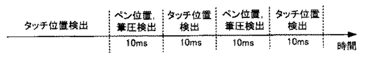
ここで、この例の位置検出器210におけるタッチパネルとしての機能とタブレットとしての機能の動作例を簡単に説明する。図23に示す例では、タッチパネルの動作とタブレットとしての動作を所定時間毎に切り換える。具体的には、中央演算処理部62と協働する制御部63の制御に従い、第1切替部232及び第2切替部233を所定時間毎に連動させて切り換えることで、指及びペン等の指示体の存在あるいは指示体が指示する位置を検出する。この例では、所定間隔(図23の例では例えば10ms)でペン形状の指示体147の位置検出動作(タブレット機能)と、指148a,148bによるタッチ位置の検出動作(タッチパネル機能)とを交互に繰り返す。
Here, an operation example of a function as a touch panel and a function as a tablet in the position detector 210 of this example will be briefly described. In the example shown in FIG. 23, the operation of the touch panel and the operation as a tablet are switched every predetermined time. Specifically, in accordance with the control of the
なお、この例の位置検出器210の動作は、図23の例に示す時分割動作に限定されない。例えば、時分割動作を採用することなく、センサ部30上で指及びペンで代表される複数種類の指示体の存在を同時に検出することもできる。この場合、位置検出器210は、次のようにして動作する。なお、以下の動作例では、ペンからは、第1の拡散符号及び該第1の拡散符号とは異なる第2の拡散符号が送信され、図22における拡散符号生成部231からは、ペンに割り当てられた第1及び第2の拡散符号とは異なる第3の拡散符号を備える送信信号を生成して出力される場合を想定する。
The operation of the position detection can 210 in this embodiment is not limited to time-division action shown in the example of FIG. 23. For example, it is also possible to simultaneously detect the presence of a plurality of types of indicators represented by fingers and pens on the sensor unit 30 without adopting a time division operation. In this case, the position detection can 210 operates as follows. In the following operation example, the pen transmits the first spreading code and the second spreading code different from the first spreading code, and the spreading
まず、拡散符号生成部231は、第3の拡散符号を備える送信信号を生成し、その送信信号を第1切替部232のスイッチSW1、第1選択回路221を介して第1導体群32を構成する複数の第1の導体31に所定の順序で繰り返し供給する。この際、受信系回路群51を構成する受信アンプ52には、第2選択回路222及び第2切替部233を介して、選択された導体が接続される。なお、第2選択回路222は、第2導体群34を構成する複数の第2導体33に対して、所定の順序による選択動作によって所定の導体を選択する。
First, the spreading
次いで、A/D変換回路53は、受信アンプ52から出力されたアナログ信号を、1ワードが所定のビット数から成るデジタル信号に変換する。次いで、シリアルパラレル変換部54及びシフトレジスタ55は、使用する拡散符号(C1、C2、C3)の符号長に対応したワード長に直列並列変換し、その変換した信号を相関演算器56に供給する。
Next, the A /
次いで、相関演算器56は、供給されたデジタル信号と各相関演算用符号との相関演算を行う。これにより、第1、第2、及び第3の拡散符号(C1、C2、C3)のそれぞれの有無を検出するとともに、その信号レベルも検出する。
Next, the
すなわち、上記の動作は、タッチ位置の検出動作(タッチパネル機能)を検出するための動作と同じである。従って、この動作状態における指位置の検出動作は既述した通りである。この動作状態において、ペンが操作された場合には、ペンから送信された第1の拡散符号C1及び第2の拡散符号C2の少なくとも一方の拡散符号を相関演算器56にて検出することでペンの存在の確認あるいはペンの指示位置を認識できる。そして、ペン操作の有無の認識に基づいて位置検出器210の機能をタブレットとしての機能に切り換えることで、ペン位置が2次元的に検出できる。
That is, the above operation is the same as the operation for detecting the touch position detection operation (touch panel function). Therefore, the finger position detection operation in this operation state is as described above. In this operation state, when the pen is operated, the
また、位置検出回路230において、指及びペンという2つの種類の指示体が同時に検出された場合には、図23に示したようにタッチパネル機能とタブレット機能を時分割的に切り換えることで、あたかも指とペンの操作を同時に検出しているかのような状態にすることができる。また、ペンと指が同時に検出された場合には、ペンあるいは指の一方を検出するための動作(タッチパネル機能あるいはタブレット機能)に移行するように機能設定を切り換えることもできる。 When the position detection circuit 230 detects two types of pointers such as a finger and a pen at the same time, the touch panel function and the tablet function are switched in a time-sharing manner as shown in FIG. And the operation of the pen at the same time. In addition, when a pen and a finger are detected at the same time, the function setting can be switched so as to shift to an operation (touch panel function or tablet function) for detecting one of the pen and the finger.
また、この例において、位置検出器210をタッチパネルとして動作させる際、互いに位相の異なる複数の拡散符号を対応する複数の第1導体31に同時供給して、複数の拡散符号を位相多重送信してもよい。例えば、n本から構成される第1導体31に対して、拡散符号生成部231で1つの符号パターンの拡散符号から互いに位相の異なるn本の拡散符号を生成し、第1導体31の各々に対応させて供給する。あるいは、n本から構成される第1導体31に対して、互いに符号パターンが異なるn種類の符号パターンの拡散符号を生成して、第1導体31の各々に対応させて供給してもよい。
Further, in this example, when the position detector 210 is operated as a touch panel, a plurality of spreading codes having different phases are simultaneously supplied to the corresponding
この場合、受信系回路群51においては、拡散符号生成部231で生成された拡散符号に対応した相関演算用符号を備え、受信された各々の拡散符号との相関演算を同時に行う構成を採用することができる。なお、この構成においては、選択回路220を構成する第1選択回路221及び第2選択回路222の少なくとも一方の回路は必ずしも必要とされない。
In this case, the reception
また、この例の位置検出器210では、指示体としての指を検出するためのタッチパネル機能と、他の種類の指示体としてのペンを検出するためのペンタブレット機能とを時分割で切り替える構成を備えるものであるが、いずれの機能で動作する場合でも第2導体群34を構成する第2導体33は常に信号受信に供される。従って、上述したように、受信系回路群51が、指示体としての指を検出するために使用される拡散符号生成部231から供給される送信信号と、他の種類の指示体としてのペンから供給される送信信号とを同時に検出可能な回路構成を備えることで、x方向における指位置を求める際にペン位置も同時に求めることができる。それゆえ、ペン位置を求める次の処理としては、x方向でのペン位置は既に取得されているために、y方向におけるペン位置を求めれば良いことになる。したがって、この例の位置検出器210では、上述のような回路構成を備えることで、センサ部30におけるペンと指の同時検出を高速に行うことができる。
Further, the position detector 210 of this example has a configuration in which a touch panel function for detecting a finger as an indicator and a pen tablet function for detecting a pen as another type of indicator are switched in a time-sharing manner. Although provided, the
更には、図12(変形例2)に示すサイドスイッチ113の操作有無の検出に関し、サイドスイッチ113からの操作信号を図3の遅延設定回路142に供給し、電位Vthを切り替える構成を備えることでサイドスイッチ113が操作されたことを検出することができる。すなわち、サイドスイッチ113が操作されたことに対応して遅延設定回路142で設定される電位Vthを、例えば高電位に切り替える。電位Vthが高電位に設定されると、指示体による押圧力が同一であっても、遅延設定回路12からの出力される信号が更に所定の時間遅延されて出力されることになる。この構成によって、サイドスイッチ113の操作に対応して、第1符号生成部から出力される信号に対する第2符号生成部から出力される信号の生成タイミングが制御されることになり、この結果、サイドスイッチ113の操作有無を検出することができる。
Furthermore, regarding the detection of the presence / absence of operation of the
更には、図2に示す指示体2、図12(a)及び(b)に示す指示体110及び117、図14に示す指示体120、図17に示す指示体130などでは、第1符号生成部26、第2符号生成部27、あるいは第3符号生成部29から出力されるそれぞれの信号を対応する第1電極20及び第2電極21に供給する構成が示されているが、この構成に限るものではない。すなわち、各々の信号を、抵抗などを介して信号加算し、第1電極20あるいは第2電極21に供給することもできる。この構成によれば、第1電極20あるいは第2電極21への信号供給点を少なくすることができ、指示体としての構成を簡単化することができる。
Further, the
上記実施形態及び変形例1〜7では、センサ部の励磁コイルからの励磁信号を受信して、指示体内の集積回路の駆動電圧を生成する例を説明したが、本発明はこれに限定されず、指示体内部に例えば蓄電池のような電源を備えていてもよい。
In the above embodiment and
1…位置検出装置、2…指示体、3…位置検出器、20…第1電極、21…第2電極、22…可変容量コンデンサ、23…集積回路、24…コイル、25…電源生成回路、26…第1符号生成部、27…第2符号生成部、28…送信符号生成部、30…センサ部、31…第1導体、32…第1導体群、33…第2導体、34…第2導体群、40…選択回路、50…位置検出回路、51…受信系回路群、52…受信アンプ、53…A/D変換回路、54…シリアルパラレル変換部、55…シフトレジスタ、56…相関演算部、56a…第1相関器、56b…第2相関器、57…記憶部、58…位置及び筆圧算出部、60…発振器、61…ドライブ回路、62…中央演算処理部、63…制御部、129…筐体
DESCRIPTION OF
Claims (34)
所定方向に配置された複数の第1の導体と前記所定方向と交差する方向に配置された複数の第2の導体を備え前記指示体から送信された信号を受信するためのセンサ部と、
前記複数の第1の導体を構成する導体と前記複数の第2の導体を構成する導体にそれぞれ生起した信号と前記2つの符号に対応した相関演算用符号との相関演算を行うための相関演算回路と、
前記相関演算回路によって算出された少なくとも1つの符号に基づく相関演算結果から前記指示体によって指示されたセンサ部上の位置を検出するための位置算出回路と、
前記相関演算回路によって算出された2つの符号に基づく相関演算結果から前記2つの符号間の時間差に対応して前記指示体に印加された圧力を検出する筆圧算出回路と、
を備えたことを特徴とする位置検出装置。 An indicator for transmitting a signal generated by the transmission signal generator, comprising a transmission signal generator for transmitting the two codes in association with a time difference between the two applied codes;
A sensor unit that includes a plurality of first conductors arranged in a predetermined direction and a plurality of second conductors arranged in a direction crossing the predetermined direction, and for receiving a signal transmitted from the indicator;
Correlation calculation for performing a correlation calculation between signals generated in the conductors constituting the plurality of first conductors and the conductors constituting the plurality of second conductors and the correlation calculation codes corresponding to the two codes. Circuit,
A position calculation circuit for detecting a position on the sensor unit indicated by the indicator from a correlation calculation result based on at least one code calculated by the correlation calculation circuit;
A writing pressure calculation circuit for detecting a pressure applied to the indicator corresponding to a time difference between the two codes from a correlation calculation result based on the two codes calculated by the correlation calculation circuit;
A position detection device comprising:
前記先端部に印加された圧力を、相関演算により識別可能なパターンを有する2つの符号間の時間差に対応づけて前記2つの符号を送信するための送信信号生成部を備え、
前記送信信号生成部によって生成された複数の符号が送信されるようにしたことを特徴
とする指示体。 An indicator provided with a tip portion for instructing a position protruding from the housing,
A transmission signal generating unit for transmitting the two codes in association with the time difference between the two codes having a pattern that can be identified by a correlation calculation with the pressure applied to the tip part;
An indicator characterized in that a plurality of codes generated by the transmission signal generator are transmitted.
所定方向に配置された複数の第1の導体と前記所定方向と交差する方向に配置された複数の第2の導体を介して前記指示体から送信された符号を受信する信号受信ステップと、
前記複数の第1の導体を構成する導体と前記複数の第2の導体を構成する導体にそれぞれ生起した信号を受信し前記2つの符号に対応した相関演算用符号との相関演算を行う相関演算処理ステップと、
前記相関演算処理ステップによって算出された1つの符号に基づく相関演算結果から前記指示体によって指示されたセンサ部上の位置を検出する位置算出ステップと、
前記相関演算処理ステップによって算出された2つの符号に基づく相関演算結果から前記指示体に印加された圧力を検出する筆圧算出ステップと、
を備えたことを特徴とする位置検出方法。 A code transmission step for transmitting two codes having a time difference corresponding to a pressure applied to a pen tip provided on the indicator for position indication;
A signal receiving step of receiving a code transmitted from the indicator through a plurality of first conductors arranged in a predetermined direction and a plurality of second conductors arranged in a direction crossing the predetermined direction;
Correlation calculation that receives signals generated in the conductors forming the plurality of first conductors and the conductors forming the plurality of second conductors and performs correlation calculation with the correlation calculation codes corresponding to the two codes Processing steps;
A position calculation step of detecting a position on the sensor unit indicated by the indicator from a correlation calculation result based on one code calculated by the correlation calculation processing step;
A writing pressure calculation step of detecting a pressure applied to the indicator from a correlation calculation result based on the two codes calculated by the correlation calculation processing step;
A position detection method comprising:
他の符号と相関演算により識別可能なパターンを有する第1の符号を送信するステップと、
前記他の符号と相関演算により識別可能なパターンを有する第2の符号を、前記先端部に印加された圧力に対応する時間をおいて送信するステップと、
を含む圧力情報送信方法。 A pressure information transmission method for transmitting a pressure applied to the tip portion of an indicator provided with a tip portion for indicating a position protruding from a housing ,
Transmitting a first code having a pattern identifiable by correlation calculation with other codes;
Transmitting a second code having a pattern identifiable by correlation calculation with the other code at a time corresponding to the pressure applied to the tip;
Including pressure information transmission method.
他の符号と相関演算により識別可能なパターンを有する第1の符号を電極片に供給するステップと、
前記他の符号と相関演算により識別可能なパターンを有する第2の符号を他の電極片に供給し、所定の情報を送信するステップと、
を含む情報送信方法。 An information transmission method from an indicator that transmits predetermined information in association with a transmission signal,
Supplying to the electrode pieces a first code having a pattern distinguishable by correlation calculation with other codes;
Supplying a second code having a pattern identifiable by correlation calculation with the other code to the other electrode piece, and transmitting predetermined information;
Information transmission method.
Priority Applications (23)
| Application Number | Priority Date | Filing Date | Title |
|---|---|---|---|
| JP2010024858A JP5442479B2 (en) | 2010-02-05 | 2010-02-05 | Indicator, position detection device and position detection method |
| US12/877,780 US8963889B2 (en) | 2010-02-05 | 2010-09-08 | Pointer, position detection apparatus and position detection method |
| IL208921A IL208921A (en) | 2010-02-05 | 2010-10-25 | Pointer, position detection apparatus and position detection method |
| CN201010593023.XA CN102147675B (en) | 2010-02-05 | 2010-12-14 | Indication body, position detecting device and method for detecting position |
| EP11150998.0A EP2354909B1 (en) | 2010-02-05 | 2011-01-14 | Pointer, position detector and position detection method |
| TW100102860A TWI507928B (en) | 2010-02-05 | 2011-01-26 | Pointer, position detection apparatus and position detection method |
| TW105126775A TWI573046B (en) | 2010-02-05 | 2011-01-26 | Position indicator |
| TW104126247A TWI569175B (en) | 2010-02-05 | 2011-01-26 | A pointer detection device and a pointer detection circuit |
| TW104126246A TWI539330B (en) | 2010-02-05 | 2011-01-26 | Indicator |
| TW104126245A TWI559177B (en) | 2010-02-05 | 2011-01-26 | A pointer, an angle information detection circuit, and a position detection device |
| KR1020110009600A KR101770431B1 (en) | 2010-02-05 | 2011-01-31 | Pointer, transmission signal generation circuit, pointer condition detection circuit and position detection apparatus |
| US14/542,438 US9529456B2 (en) | 2010-02-05 | 2014-11-14 | Pointer, position detection apparatus and position detection method |
| US14/542,462 US9606640B2 (en) | 2010-02-05 | 2014-11-14 | Pointer, position detection apparatus and position detection method |
| US14/542,480 US9632599B2 (en) | 2010-02-05 | 2014-11-14 | Pointer, position detection apparatus and position detection method |
| US15/047,013 US10108277B2 (en) | 2010-02-05 | 2016-02-18 | Pointer, position detection apparatus and position detection method |
| KR1020170102929A KR101878103B1 (en) | 2010-02-05 | 2017-08-14 | Pointer and method for providing angle information of the pointer |
| US15/811,233 US10423247B2 (en) | 2010-02-05 | 2017-11-13 | Pointer, position detection apparatus and position detection method |
| US15/896,984 US10514781B2 (en) | 2010-02-05 | 2018-02-14 | Pointer, position detection apparatus and position detection method |
| US15/928,978 US10429955B2 (en) | 2010-02-05 | 2018-03-22 | Pointer, position detection apparatus and position detection method |
| US16/019,327 US10437353B2 (en) | 2010-02-05 | 2018-06-26 | Pointer, position detection apparatus and position detection method |
| US16/689,830 US11099661B2 (en) | 2010-02-05 | 2019-11-20 | Pointer, position detection apparatus and position detection method |
| US17/379,747 US11853485B2 (en) | 2010-02-05 | 2021-07-19 | Pointer, position detection apparatus and position detection method |
| US18/509,096 US20240077960A1 (en) | 2010-02-05 | 2023-11-14 | Pointer, position detection apparatus and position detection method |
Applications Claiming Priority (1)
| Application Number | Priority Date | Filing Date | Title |
|---|---|---|---|
| JP2010024858A JP5442479B2 (en) | 2010-02-05 | 2010-02-05 | Indicator, position detection device and position detection method |
Publications (3)
| Publication Number | Publication Date |
|---|---|
| JP2011164801A JP2011164801A (en) | 2011-08-25 |
| JP2011164801A5 JP2011164801A5 (en) | 2013-03-21 |
| JP5442479B2 true JP5442479B2 (en) | 2014-03-12 |
Family
ID=43805766
Family Applications (1)
| Application Number | Title | Priority Date | Filing Date |
|---|---|---|---|
| JP2010024858A Active JP5442479B2 (en) | 2010-02-05 | 2010-02-05 | Indicator, position detection device and position detection method |
Country Status (7)
| Country | Link |
|---|---|
| US (12) | US8963889B2 (en) |
| EP (1) | EP2354909B1 (en) |
| JP (1) | JP5442479B2 (en) |
| KR (2) | KR101770431B1 (en) |
| CN (1) | CN102147675B (en) |
| IL (1) | IL208921A (en) |
| TW (5) | TWI507928B (en) |
Cited By (1)
| Publication number | Priority date | Publication date | Assignee | Title |
|---|---|---|---|---|
| US11360586B2 (en) | 2017-11-29 | 2022-06-14 | Wacom Co., Ltd. | Communication method executed between active pen and sensor controller, and active pen |
Families Citing this family (117)
| Publication number | Priority date | Publication date | Assignee | Title |
|---|---|---|---|---|
| US20090174676A1 (en) | 2008-01-04 | 2009-07-09 | Apple Inc. | Motion component dominance factors for motion locking of touch sensor data |
| JP5430339B2 (en) * | 2009-10-19 | 2014-02-26 | 株式会社ワコム | Position detecting device and position indicator |
| JP5442479B2 (en) | 2010-02-05 | 2014-03-12 | 株式会社ワコム | Indicator, position detection device and position detection method |
| US8766954B2 (en) * | 2010-12-21 | 2014-07-01 | Motorola Mobility Llc | Active stylus for use with touch-sensitive interfaces and corresponding method |
| US9122322B2 (en) * | 2011-03-17 | 2015-09-01 | Microsoft Technology Licensing, Llc | Interacting tips for a digitizer stylus |
| US8878823B1 (en) | 2011-07-27 | 2014-11-04 | Cypress Semiconductor Corporation | Dynamic shield electrode of a stylus |
| KR101355938B1 (en) * | 2011-09-23 | 2014-01-28 | 주식회사 더한 | Electronic pen for tablet |
| CN102509613B (en) * | 2011-09-27 | 2014-06-18 | 汉王科技股份有限公司 | Variable capacitor and position indicator using same |
| US9134849B2 (en) | 2011-10-25 | 2015-09-15 | Nook Digital, Llc | Pen interface for a touch screen device |
| US10082889B2 (en) | 2011-10-28 | 2018-09-25 | Atmel Corporation | Multi-electrode active stylus tip |
| CN102566800B (en) * | 2011-12-29 | 2015-08-12 | 敦泰科技有限公司 | A kind of felt pen, touch detecting method and touch detecting system |
| KR101282430B1 (en) * | 2012-03-26 | 2013-07-04 | 삼성디스플레이 주식회사 | Stylus, pressure detecting system and the driving method thereof |
| US9201521B2 (en) * | 2012-06-08 | 2015-12-01 | Qualcomm Incorporated | Storing trace information |
| JP6021174B2 (en) * | 2012-08-08 | 2016-11-09 | 株式会社ワコム | Position detecting device and position indicator thereof |
| US9354737B2 (en) * | 2012-08-09 | 2016-05-31 | Atmel Corporation | Active stylus self-capacitance measurement |
| CN103973154B (en) * | 2013-01-28 | 2016-07-06 | 北京大学科技开发部 | A kind of single friction surface microgenerator and manufacture method thereof |
| US9946365B2 (en) * | 2013-03-11 | 2018-04-17 | Barnes & Noble College Booksellers, Llc | Stylus-based pressure-sensitive area for UI control of computing device |
| US9766723B2 (en) | 2013-03-11 | 2017-09-19 | Barnes & Noble College Booksellers, Llc | Stylus sensitive device with hover over stylus control functionality |
| US9785259B2 (en) | 2013-03-11 | 2017-10-10 | Barnes & Noble College Booksellers, Llc | Stylus-based slider functionality for UI control of computing device |
| US10048775B2 (en) | 2013-03-14 | 2018-08-14 | Apple Inc. | Stylus detection and demodulation |
| EP2972695B1 (en) * | 2013-03-15 | 2020-01-01 | Tactual Labs Co. | Stylus and fast multi-touch sensor |
| KR102288703B1 (en) * | 2013-03-15 | 2021-08-11 | 텍추얼 랩스 컴퍼니 | Fast multi-touch stylus and sensor |
| JP6105054B2 (en) * | 2013-04-05 | 2017-03-29 | シャープ株式会社 | Touch panel position detection method, touch panel controller, touch panel system, and electronic device |
| WO2014181680A1 (en) * | 2013-05-10 | 2014-11-13 | シャープ株式会社 | Touch panel system, stylus pen, and electronic device |
| US9495056B2 (en) | 2013-05-21 | 2016-11-15 | Sharp Kabushiki Kaisha | Touch panel system and electronic device |
| WO2014196350A1 (en) * | 2013-06-07 | 2014-12-11 | シャープ株式会社 | Touch panel system and electronic device |
| JP5647715B1 (en) * | 2013-06-27 | 2015-01-07 | 株式会社ワコム | Position indicator |
| TWI518557B (en) * | 2013-07-17 | 2016-01-21 | 恆顥科技股份有限公司 | Projective capacitive stylus and controlling method thereof |
| JP2015023723A (en) * | 2013-07-22 | 2015-02-02 | 船井電機株式会社 | Power supply device and non-power supply target detection method |
| US10067580B2 (en) | 2013-07-31 | 2018-09-04 | Apple Inc. | Active stylus for use with touch controller architecture |
| KR20160028484A (en) * | 2013-08-20 | 2016-03-11 | 어드밴스드 실리콘 에스아 | Capacitive touch system |
| KR101631996B1 (en) * | 2014-08-01 | 2016-06-21 | 엘지전자 주식회사 | Mobile terminal comprising a stylus pen and a touch panel |
| WO2015030452A1 (en) * | 2013-08-30 | 2015-03-05 | 엘지전자 주식회사 | Mobile terminal comprising stylus pen and touch panel |
| US9513721B2 (en) | 2013-09-12 | 2016-12-06 | Microsoft Technology Licensing, Llc | Pressure sensitive stylus for a digitizer |
| TWI498793B (en) * | 2013-09-18 | 2015-09-01 | Wistron Corp | Optical touch system and control method |
| KR102161446B1 (en) | 2013-11-05 | 2020-10-05 | 삼성전자 주식회사 | Electronic device including a touch-based user interface |
| US11409379B2 (en) * | 2013-11-08 | 2022-08-09 | Egalax_Empia Technology Inc. | Stylus and operating method thereof for transmitting electrical signals carrying pressure information |
| US10503318B2 (en) * | 2015-06-16 | 2019-12-10 | Egalax_Empia Technology Inc. | Touch sensitive processing apparatus and system for despreading and method thereof |
| US10890987B2 (en) * | 2013-11-08 | 2021-01-12 | Egalax_Empia Technology Inc. | Stylus and operating method thereof for transmitting electrical signals carrying pressure information |
| US11392221B2 (en) * | 2013-11-08 | 2022-07-19 | Egalax_Empia Technology Inc. | Touch sensitive processing apparatus, system and operating method thereof for receiving electrical signals carrying pressure information |
| US10895921B2 (en) | 2013-11-08 | 2021-01-19 | Egalax_Empia Technology Inc. | Touch sensitive processing apparatus, system and operating method thereof for receiving electrical signals carrying pressure information |
| WO2015079861A1 (en) * | 2013-11-27 | 2015-06-04 | 株式会社ワコム | Electronic instrument |
| KR102293319B1 (en) * | 2013-12-25 | 2021-08-25 | 가부시키가이샤 와코무 | Position indicating module and stylus pen |
| CN105934734B (en) * | 2014-01-22 | 2020-11-20 | 株式会社和冠 | Position indicator, position detection device, position detection circuit, and position detection method |
| TWI480770B (en) * | 2014-06-27 | 2015-04-11 | Waltop Int Corp | Capacitive pointer |
| EP3168716B1 (en) * | 2014-07-08 | 2020-09-09 | Wacom Co., Ltd. | Position indicator |
| WO2016031059A1 (en) * | 2014-08-29 | 2016-03-03 | 株式会社ワコム | Position indicator and position detector |
| CN107077260B (en) | 2014-09-22 | 2020-05-12 | 苹果公司 | Touch controller and method for touch sensor panel |
| WO2016063420A1 (en) * | 2014-10-24 | 2016-04-28 | 株式会社ワコム | Transmission-type electronic pen |
| US10712867B2 (en) | 2014-10-27 | 2020-07-14 | Apple Inc. | Pixelated self-capacitance water rejection |
| US9874951B2 (en) | 2014-11-03 | 2018-01-23 | Microsoft Technology Licensing, Llc | Stylus for operating a digitizer system |
| EP3223118B1 (en) * | 2014-11-17 | 2019-12-25 | Wacom Co., Ltd. | Position indicator |
| US10067618B2 (en) | 2014-12-04 | 2018-09-04 | Apple Inc. | Coarse scan and targeted active mode scan for touch |
| US9830000B2 (en) * | 2014-12-12 | 2017-11-28 | Microsoft Technology Licensing, Llc | Active stylus synchronization |
| JP6487694B2 (en) * | 2014-12-26 | 2019-03-20 | 株式会社ワコム | Position indicator and signal processing device |
| CN113031791B (en) * | 2015-01-19 | 2024-04-16 | 株式会社和冠 | Position indicator |
| KR101672731B1 (en) * | 2015-01-20 | 2016-11-04 | 주식회사 트레이스 | 3d hovering digitizer system using pen tilt |
| WO2016121045A1 (en) * | 2015-01-29 | 2016-08-04 | 株式会社ワコム | Electrostatic pen |
| CN107209602B (en) * | 2015-02-02 | 2020-05-26 | 苹果公司 | Flexible self-capacitance and mutual capacitance touch sensing system architecture |
| WO2016132627A1 (en) * | 2015-02-18 | 2016-08-25 | ソニー株式会社 | Information processing device and information processing method |
| JP6544791B2 (en) * | 2015-02-20 | 2019-07-17 | 株式会社ワコム | Position indicator, signal processing circuit, signal supply control method and signal processing method |
| CN106471446B (en) * | 2015-03-26 | 2019-06-11 | 华为技术有限公司 | Drawing pen, electronic equipment and drawing practice |
| US9785275B2 (en) | 2015-03-30 | 2017-10-10 | Wacom Co., Ltd. | Contact discrimination using a tilt angle of a touch-sensitive surface |
| US9448646B1 (en) * | 2015-04-20 | 2016-09-20 | Wacom Co., Ltd. | System and method for bidirectional communication between stylus and stylus sensor controller |
| CN111913606A (en) * | 2015-04-20 | 2020-11-10 | 株式会社和冠 | Sensor controller, host processor, communication method and system |
| KR102444210B1 (en) | 2015-04-20 | 2022-09-19 | 가부시키가이샤 와코무 | Method using active stylus and sensor controller, sensor controller, active stylus, and system |
| CN107533384B (en) | 2015-04-20 | 2020-10-20 | 株式会社和冠 | Method using active stylus and sensor controller, and active stylus |
| US9785262B2 (en) | 2015-04-20 | 2017-10-10 | Wacom Co., Ltd. | System and method for bidirectional communication between stylus and stylus sensor controller |
| US9874966B2 (en) * | 2015-04-28 | 2018-01-23 | Microsoft Technology Licensing, Llc | Electrostatic device having spaced electrodes |
| EP3091422B1 (en) * | 2015-05-08 | 2020-06-24 | Nokia Technologies Oy | Method, apparatus and computer program product for entering operational states based on an input type |
| EP3299936B1 (en) * | 2015-05-21 | 2020-01-01 | Wacom Co., Ltd. | Active stylus |
| US9606662B2 (en) * | 2015-06-10 | 2017-03-28 | International Business Machines Corporation | Touch interface with person recognition |
| CN106716314B (en) | 2015-07-06 | 2020-02-28 | 3轴数据有限责任公司 | Pen system with internal pressure inclined rotation |
| CN107850951B (en) * | 2015-08-19 | 2020-12-18 | 株式会社和冠 | Method for detecting sensor controller by stylus, stylus and sensor controller |
| JP6487807B2 (en) * | 2015-08-21 | 2019-03-20 | 株式会社ワコム | Position indicator |
| US9740312B2 (en) | 2015-09-09 | 2017-08-22 | Microsoft Technology Licensing, Llc | Pressure sensitive stylus |
| WO2017044975A1 (en) * | 2015-09-11 | 2017-03-16 | Tactual Labs Co. | Semi-passive stylus |
| US10162435B2 (en) | 2016-01-04 | 2018-12-25 | Asustek Computer Inc. | Input device and input method using the same |
| KR102456350B1 (en) * | 2016-01-28 | 2022-10-20 | 엘지디스플레이 주식회사 | Active stylus pen and touch sensing system and driving method of the same |
| CN107390898B (en) * | 2016-03-08 | 2020-10-30 | 禾瑞亚科技股份有限公司 | Touch control pen providing inclination angle and pen body axial direction and control method thereof |
| US9841828B2 (en) | 2016-04-20 | 2017-12-12 | Microsoft Technology Licensing, Llc | Pressure sensitive stylus |
| KR102523154B1 (en) * | 2016-04-22 | 2023-04-21 | 삼성전자주식회사 | Display apparatus, input device and control method thereof |
| US10474277B2 (en) * | 2016-05-31 | 2019-11-12 | Apple Inc. | Position-based stylus communication |
| JP6756525B2 (en) * | 2016-06-16 | 2020-09-16 | 株式会社ワコム | Writing implements and electronic pen body |
| KR20180015987A (en) | 2016-08-04 | 2018-02-14 | 삼성전자주식회사 | Touch sensing device for determining infomration associated with pen and method for controlling thereof and pen |
| WO2018029855A1 (en) * | 2016-08-12 | 2018-02-15 | 株式会社ワコム | Stylus and sensor controller |
| KR102509605B1 (en) * | 2016-09-06 | 2023-03-14 | 삼성디스플레이 주식회사 | Stylus pen, touch sensor, and driving method of touch sensor |
| US10474286B2 (en) * | 2016-10-25 | 2019-11-12 | Lg Display Co., Ltd. | Touch display device, active pen, touch system, touch circuit, and pen recognition method |
| KR102616491B1 (en) * | 2016-11-03 | 2023-12-21 | 엘지전자 주식회사 | Touch input apparatus using a stylus pen and method for detecting touch thereof |
| TWI622902B (en) * | 2016-11-04 | 2018-05-01 | 宏碁股份有限公司 | Touch control system and method for determining tilt state of stylus device |
| US10613676B2 (en) * | 2016-11-04 | 2020-04-07 | Microsoft Technology Licensing, Llc | Non-uniform code constellations in electrostatic communication |
| US10331235B2 (en) * | 2016-11-23 | 2019-06-25 | Wacom Co., Ltd. | Stylus tilt detection based on bidirectional communication between stylus and stylus sensor controller |
| TWI613636B (en) | 2016-12-28 | 2018-02-01 | 財團法人工業技術研究院 | Driving device and driving method |
| KR102460472B1 (en) * | 2016-12-30 | 2022-11-01 | 엘지디스플레이 주식회사 | Touch sensing system, display device, active pen, and pen recognizing method |
| TWI621972B (en) | 2017-01-12 | 2018-04-21 | 奇景光電股份有限公司 | Touch display apparatus and method for touch display panel |
| US10318022B2 (en) | 2017-01-30 | 2019-06-11 | Microsoft Technology Licensing, Llc | Pressure sensitive stylus |
| JP6952472B2 (en) | 2017-02-06 | 2021-10-20 | エルジー ディスプレイ カンパニー リミテッド | Tilt derivation device and tilt derivation method |
| JP6962690B2 (en) | 2017-02-06 | 2021-11-05 | エルジー ディスプレイ カンパニー リミテッド | Tilt derivation device and tilt derivation method |
| CN117348745A (en) * | 2017-02-22 | 2024-01-05 | 株式会社和冠 | Active stylus and controller integrated circuit in active stylus |
| KR102303136B1 (en) * | 2017-03-16 | 2021-09-17 | 삼성전자주식회사 | Input device, electronic system and control method thereof |
| KR102303139B1 (en) * | 2017-03-16 | 2021-09-17 | 삼성전자주식회사 | Input device, electronic system and control method thereof |
| JP6962710B2 (en) | 2017-05-29 | 2021-11-05 | エルジー ディスプレイ カンパニー リミテッド | Tilt derivation device and tilt derivation method |
| JP6846285B2 (en) | 2017-05-29 | 2021-03-24 | エルジー ディスプレイ カンパニー リミテッド | Position detection device and position detection method |
| JP6902397B2 (en) | 2017-05-29 | 2021-07-14 | エルジー ディスプレイ カンパニー リミテッド | Tilt derivation device and tilt derivation method |
| JP7132933B2 (en) * | 2017-09-27 | 2022-09-07 | 株式会社ワコム | position indicator |
| EP3702890B1 (en) * | 2017-10-25 | 2023-03-15 | Wacom Co., Ltd. | Position indicator and associated method and system |
| KR102468750B1 (en) | 2017-12-29 | 2022-11-18 | 엘지디스플레이 주식회사 | Touch display device, touch system, touch driving circuit, and pen sensing method |
| TWM570464U (en) * | 2018-08-22 | 2018-11-21 | 宏碁股份有限公司 | Capacitive stylus |
| CN111758084A (en) * | 2019-01-29 | 2020-10-09 | 深圳市汇顶科技股份有限公司 | Pressure calculation method and device, electronic equipment and touch system |
| US10928946B2 (en) * | 2019-02-15 | 2021-02-23 | Dell Products L.P. | Touchscreen stylus and display module interface |
| JP7300304B2 (en) * | 2019-04-22 | 2023-06-29 | 株式会社ワコム | PEN STATE DETECTION CIRCUIT AND PEN STATE DETECTION METHOD |
| US11281314B2 (en) * | 2019-12-02 | 2022-03-22 | Semiconductor Components Industries, Llc | Methods and apparatus for variable capacitance detection |
| WO2021111629A1 (en) * | 2019-12-06 | 2021-06-10 | 三菱電機株式会社 | Correction information calculation device, correction information calculation system, correction information calculation method, and correction information calculation program |
| US11662867B1 (en) | 2020-05-30 | 2023-05-30 | Apple Inc. | Hover detection on a touch sensor panel |
| CN112260661A (en) * | 2020-10-21 | 2021-01-22 | 深圳市绘王动漫科技有限公司 | Signal processing circuit and position detection device |
| WO2022094802A1 (en) * | 2020-11-04 | 2022-05-12 | 深圳市汇顶科技股份有限公司 | Active capacitive stylus and electronic terminal |
| US11656726B1 (en) * | 2022-02-09 | 2023-05-23 | Novatek Microelectronics Corp. | Control circuit, electronic device, and control method for stylus pen interacting with touch panel |
Family Cites Families (103)
| Publication number | Priority date | Publication date | Assignee | Title |
|---|---|---|---|---|
| JPS53149030A (en) | 1977-05-31 | 1978-12-26 | Ricoh Co Ltd | Multi-needle electrode plate for electrostatic recording |
| US4263592A (en) | 1979-11-06 | 1981-04-21 | Pentel Kabushiki Kaisha | Input pen assembly |
| US4513437A (en) * | 1982-06-30 | 1985-04-23 | International Business Machines Corporation | Data input pen for Signature Verification |
| US4725978A (en) * | 1983-05-30 | 1988-02-16 | Ichiro Fujioka | Graphic pattern inputting apparatus |
| US5402151A (en) * | 1989-10-02 | 1995-03-28 | U.S. Philips Corporation | Data processing system with a touch screen and a digitizing tablet, both integrated in an input device |
| JP2868266B2 (en) * | 1990-01-25 | 1999-03-10 | 株式会社日本自動車部品総合研究所 | Signal phase difference detection circuit and signal phase difference detection method |
| GB9021448D0 (en) | 1990-10-03 | 1990-11-14 | Renishaw Plc | Capacitance sensing probe |
| US5117071A (en) * | 1990-10-31 | 1992-05-26 | International Business Machines Corporation | Stylus sensing system |
| US5138118A (en) * | 1991-05-06 | 1992-08-11 | International Business Machines Corporation | Pulsed pen for use with a digitizer tablet |
| US5422959A (en) * | 1993-06-25 | 1995-06-06 | Lee; Michael E. | Signature verification apparatus and method utilizing relative angle measurements |
| US5528002A (en) * | 1993-07-15 | 1996-06-18 | Pentel Kabushiki Kaisha | Noiseproof digitizing apparatus with low power cordless pen |
| JP3098899B2 (en) * | 1993-11-01 | 2000-10-16 | 富士写真フイルム株式会社 | Overturning device for long web rolls |
| JPH07200137A (en) * | 1993-12-28 | 1995-08-04 | Wacom Co Ltd | Position detection device and its position indicator |
| JP3421416B2 (en) * | 1994-03-18 | 2003-06-30 | 株式会社ワコム | Position detecting device and its position indicator |
| US5736980A (en) * | 1994-04-28 | 1998-04-07 | Sharp Kabushiki Kaisha | Coordinate inputting apparatus with shared line combinations of power, position and switch signals |
| JP3186946B2 (en) | 1994-05-31 | 2001-07-11 | シャープ株式会社 | Coordinate detection device |
| JP3272544B2 (en) * | 1994-07-18 | 2002-04-08 | 株式会社ワコム | Position detecting device and position indicator |
| EP0717368B1 (en) * | 1994-12-16 | 2001-10-04 | Hyundai Electronics America | Digitizer stylus and method of operation |
| JPH08179871A (en) * | 1994-12-20 | 1996-07-12 | Pentel Kk | Combination touch panel and transparent digitizer |
| JP3188367B2 (en) * | 1994-12-26 | 2001-07-16 | シャープ株式会社 | Coordinate detection device |
| JP3251489B2 (en) * | 1996-02-16 | 2002-01-28 | シャープ株式会社 | Coordinate input device |
| JP3837800B2 (en) * | 1996-10-31 | 2006-10-25 | 株式会社ワコム | Position indicator |
| JPH10207841A (en) * | 1997-01-22 | 1998-08-07 | Mitsubishi Electric Corp | Pen input personal information terminal equipment |
| US6184873B1 (en) * | 1998-01-20 | 2001-02-06 | Electronics For Imaging, Inc. | Pen positioning system |
| KR100595925B1 (en) * | 1998-01-26 | 2006-07-05 | 웨인 웨스터만 | Method and apparatus for integrating manual input |
| AU3987299A (en) | 1998-05-12 | 1999-11-29 | E-Ink Corporation | Microencapsulated electrophoretic electrostatically-addressed media for drawing device applications |
| EP0967566A3 (en) * | 1998-06-22 | 2002-03-13 | Wacom Co., Ltd. | Coordinate input system |
| JP2000122808A (en) * | 1998-10-19 | 2000-04-28 | Fujitsu Ltd | Input processing method and input control unit |
| US6731270B2 (en) * | 1998-10-21 | 2004-05-04 | Luidia Inc. | Piezoelectric transducer for data entry device |
| US6744426B1 (en) | 1999-08-10 | 2004-06-01 | Brother Kogyo Kabushiki Kaisha | Pen coordinate reading device with pen attribute detecting function |
| JP2001282444A (en) * | 2000-03-31 | 2001-10-12 | Brother Ind Ltd | Coordinate input tool and coordinate reader |
| WO2001048589A1 (en) * | 1999-12-28 | 2001-07-05 | Fujitsu Limited | Pen sensor coordinate narrowing method and device therefor |
| US6535206B1 (en) * | 2000-02-18 | 2003-03-18 | Intel Corporation | Ultrasonic wireless pen position determination system and method |
| US6590568B1 (en) * | 2000-11-20 | 2003-07-08 | Nokia Corporation | Touch screen drag and drop input technique |
| CN1252576C (en) * | 2000-12-15 | 2006-04-19 | 丁系统有限责任公司 | Pen type optical mouse device and method of controlling the same |
| KR100408518B1 (en) * | 2001-04-12 | 2003-12-06 | 삼성전자주식회사 | Pen input device and Measuring method of coordinate |
| ATE398803T1 (en) * | 2001-05-21 | 2008-07-15 | Synaptics Uk Ltd | POSITION SENSOR |
| FR2825499B1 (en) | 2001-06-05 | 2004-07-23 | Commissariat Energie Atomique | DEVICE AND METHOD FOR LOCATING THE TIP OF A PEN ON A SCANNING MEDIUM |
| US6850230B1 (en) | 2001-10-16 | 2005-02-01 | Hewlett-Packard Development Company, L.P. | Electronic writing and erasing pencil |
| US6882340B2 (en) * | 2001-10-19 | 2005-04-19 | Wacom Co., Ltd. | Electronic pen |
| JP3957505B2 (en) * | 2001-12-26 | 2007-08-15 | 株式会社ワコム | 3D information detection device, 3D information sensor device |
| US7109979B2 (en) * | 2002-02-08 | 2006-09-19 | Virtual Ink Corporation | System and method for recording writing performed on a surface |
| GB2403017A (en) * | 2002-03-05 | 2004-12-22 | Synaptics | Position sensor |
| AU2003227021A1 (en) * | 2002-03-13 | 2003-09-22 | Jonas Ove Philip Eliasson | A touch pad, a stylus for use with the touch pad, and a method of operating the touch pad |
| KR100974022B1 (en) * | 2002-04-15 | 2010-11-15 | 에포스 디벨롭먼트 리미티드 | Method and system for obtaining positioning data |
| JP2004005415A (en) * | 2002-04-19 | 2004-01-08 | Sharp Corp | Input device and input/output integrated display |
| CN1194282C (en) * | 2002-04-22 | 2005-03-23 | 北京汉王科技有限公司 | Wireless passive hand-writing board for computer log-in |
| US20030214490A1 (en) * | 2002-05-20 | 2003-11-20 | Gateway, Inc. | Stylus providing variable line width as a function of pressure |
| GB0213237D0 (en) * | 2002-06-07 | 2002-07-17 | Koninkl Philips Electronics Nv | Input system |
| EP1529315A4 (en) * | 2002-07-22 | 2006-10-18 | Measurement Spec Inc | Handheld device having ultrasonic transducer for axial transmission of acoustic signals |
| US20040056849A1 (en) * | 2002-07-25 | 2004-03-25 | Andrew Lohbihler | Method and apparatus for powering, detecting and locating multiple touch input devices on a touch screen |
| US7489308B2 (en) * | 2003-02-14 | 2009-02-10 | Microsoft Corporation | Determining the location of the tip of an electronic stylus |
| JP4143462B2 (en) * | 2003-04-09 | 2008-09-03 | シャープ株式会社 | Pen input display device |
| KR101190657B1 (en) * | 2003-04-21 | 2012-10-15 | 삼성전자주식회사 | Manufacturing method of self-ordered nanochannel-array and manufacturing method of nano dot using the nanochannel-array |
| KR100543701B1 (en) * | 2003-06-17 | 2006-01-20 | 삼성전자주식회사 | Apparatus and method for inputting information spatially |
| US7735024B2 (en) * | 2003-10-29 | 2010-06-08 | Intel Corporation | Methods and apparatus to provide a handheld pointer-based user interface |
| JP2005149140A (en) * | 2003-11-14 | 2005-06-09 | Wacom Co Ltd | Position detector and position indicator |
| US7737953B2 (en) * | 2004-08-19 | 2010-06-15 | Synaptics Incorporated | Capacitive sensing apparatus having varying depth sensing elements |
| US7847789B2 (en) * | 2004-11-23 | 2010-12-07 | Microsoft Corporation | Reducing accidental touch-sensitive device activation |
| JP4317826B2 (en) | 2005-03-10 | 2009-08-19 | パナソニック株式会社 | Jitter detector |
| US7508384B2 (en) * | 2005-06-08 | 2009-03-24 | Daka Research Inc. | Writing system |
| US20070146351A1 (en) * | 2005-12-12 | 2007-06-28 | Yuji Katsurahira | Position input device and computer system |
| CN101009158B (en) | 2006-01-26 | 2011-05-18 | 汉王科技股份有限公司 | A capacitance-changing device |
| US7570253B2 (en) * | 2006-03-06 | 2009-08-04 | Fortemedia, Inc. | Pen-type computer |
| JP4709674B2 (en) * | 2006-03-23 | 2011-06-22 | 株式会社ワコム | Position detection apparatus and computer |
| US8297488B2 (en) * | 2006-03-28 | 2012-10-30 | Panasonic Corporation | Bump forming method using self-assembling resin and a wall surface |
| EP2040376B1 (en) * | 2006-06-13 | 2013-08-14 | Kyocera Corporation | Variable capacitance circuit |
| US7940253B2 (en) * | 2006-08-17 | 2011-05-10 | Avago Technologies Ecbu Ip (Singapore) Pte. Ltd. | Method and system for screen navigation |
| JP4345851B2 (en) * | 2006-09-11 | 2009-10-14 | ソニー株式会社 | Communication system and communication apparatus |
| JP4773315B2 (en) * | 2006-10-31 | 2011-09-14 | 株式会社ワコム | Position detecting device and position indicator |
| KR100850313B1 (en) | 2006-11-01 | 2008-08-04 | 이용직 | System and method of service for providing fixed and mobile converged handwriting instant messenger service |
| US9201556B2 (en) * | 2006-11-08 | 2015-12-01 | 3M Innovative Properties Company | Touch location sensing system and method employing sensor data fitting to a predefined curve |
| US8134542B2 (en) * | 2006-12-20 | 2012-03-13 | 3M Innovative Properties Company | Untethered stylus employing separate communication and power channels |
| US8243049B2 (en) * | 2006-12-20 | 2012-08-14 | 3M Innovative Properties Company | Untethered stylus employing low current power converter |
| US8040330B2 (en) * | 2006-12-28 | 2011-10-18 | 3M Innovative Properties Company | Untethered stylus empolying multiple reference frequency communication |
| WO2008120200A2 (en) * | 2007-03-29 | 2008-10-09 | N-Trig Ltd. | System and method for multiple object detection on a digitizer system |
| JP4872111B2 (en) | 2007-04-19 | 2012-02-08 | 株式会社ワコム | Position indicator |
| JP4872113B2 (en) * | 2007-09-10 | 2012-02-08 | 株式会社ワコム | Position detection device |
| JP5011541B2 (en) * | 2007-09-11 | 2012-08-29 | 株式会社ワコム | Position indicator |
| US8629358B2 (en) * | 2007-09-26 | 2014-01-14 | N-Trig Ltd. | Method for identifying changes in signal frequencies emitted by a stylus interacting with a digitizer sensor |
| US8184109B2 (en) | 2007-10-24 | 2012-05-22 | Wacom Co., Ltd. | Coordinate input device, position indicator and variable capacitor |
| KR101591488B1 (en) * | 2008-01-03 | 2016-02-03 | 퀄컴 테크놀로지스, 인크. | Ultrasonic digitizer and host |
| US20090278794A1 (en) * | 2008-05-09 | 2009-11-12 | Smart Technologies Ulc | Interactive Input System With Controlled Lighting |
| KR20100015225A (en) * | 2008-08-04 | 2010-02-12 | 삼성전자주식회사 | Liquid crystal display apparatus and touch sensing method thereof |
| JP5229887B2 (en) * | 2008-08-06 | 2013-07-03 | 株式会社ワコム | Position detection device |
| US8536471B2 (en) * | 2008-08-25 | 2013-09-17 | N-Trig Ltd. | Pressure sensitive stylus for a digitizer |
| JP2010067117A (en) * | 2008-09-12 | 2010-03-25 | Mitsubishi Electric Corp | Touch panel device |
| US8482545B2 (en) * | 2008-10-02 | 2013-07-09 | Wacom Co., Ltd. | Combination touch and transducer input system and method |
| GB2466566B (en) * | 2008-12-22 | 2010-12-22 | N trig ltd | Digitizer, stylus and method of synchronization therewith |
| US8278571B2 (en) * | 2009-04-03 | 2012-10-02 | Pixart Imaging Inc. | Capacitive touchscreen or touchpad for finger and active stylus |
| US9417738B2 (en) * | 2009-06-12 | 2016-08-16 | Synaptics Incorporated | Untethered active pen and a method for communicating with a capacitive sensing device using the untethered active pen |
| JP5295008B2 (en) | 2009-06-18 | 2013-09-18 | 株式会社ワコム | Indicator detection device |
| US8664548B2 (en) * | 2009-09-11 | 2014-03-04 | Apple Inc. | Touch controller with improved diagnostics calibration and communications support |
| US8766982B2 (en) * | 2010-01-19 | 2014-07-01 | Disney Enterprises, Inc. | Vectorization of line drawings using global topology and storing in hybrid form |
| JP5442479B2 (en) | 2010-02-05 | 2014-03-12 | 株式会社ワコム | Indicator, position detection device and position detection method |
| US8780061B2 (en) * | 2010-02-11 | 2014-07-15 | Lg Display Co., Ltd. | Electrostatic capacity type touch screen panel and method of manufacturing the same |
| EP2580645B1 (en) * | 2010-06-11 | 2019-11-27 | Microsoft Technology Licensing, LLC | Object orientation detection with a digitizer |
| US9239637B2 (en) * | 2010-08-30 | 2016-01-19 | Perceptive Pixel, Inc. | Systems for an electrostatic stylus within a capacitive touch sensor |
| US9507441B2 (en) | 2011-09-08 | 2016-11-29 | Jcm Electronic Stylus Llc | Electronic stylus with low skew tip for capacitive touch screens |
| US10082889B2 (en) * | 2011-10-28 | 2018-09-25 | Atmel Corporation | Multi-electrode active stylus tip |
| TWI486826B (en) * | 2011-12-19 | 2015-06-01 | Egalax Empia Technology Inc | Capacitive cordless writing appratus |
| US9030380B1 (en) * | 2013-11-21 | 2015-05-12 | R2Z Innovations Inc. | Method, a device and a system for interacting with the touch-sensitive electronic display of a computer |
| EP3299936B1 (en) * | 2015-05-21 | 2020-01-01 | Wacom Co., Ltd. | Active stylus |
-
2010
- 2010-02-05 JP JP2010024858A patent/JP5442479B2/en active Active
- 2010-09-08 US US12/877,780 patent/US8963889B2/en active Active
- 2010-10-25 IL IL208921A patent/IL208921A/en active IP Right Grant
- 2010-12-14 CN CN201010593023.XA patent/CN102147675B/en active Active
-
2011
- 2011-01-14 EP EP11150998.0A patent/EP2354909B1/en active Active
- 2011-01-26 TW TW100102860A patent/TWI507928B/en active
- 2011-01-26 TW TW105126775A patent/TWI573046B/en active
- 2011-01-26 TW TW104126247A patent/TWI569175B/en active
- 2011-01-26 TW TW104126245A patent/TWI559177B/en active
- 2011-01-26 TW TW104126246A patent/TWI539330B/en active
- 2011-01-31 KR KR1020110009600A patent/KR101770431B1/en active IP Right Grant
-
2014
- 2014-11-14 US US14/542,438 patent/US9529456B2/en active Active
- 2014-11-14 US US14/542,462 patent/US9606640B2/en active Active
- 2014-11-14 US US14/542,480 patent/US9632599B2/en active Active
-
2016
- 2016-02-18 US US15/047,013 patent/US10108277B2/en active Active
-
2017
- 2017-08-14 KR KR1020170102929A patent/KR101878103B1/en active IP Right Grant
- 2017-11-13 US US15/811,233 patent/US10423247B2/en active Active
-
2018
- 2018-02-14 US US15/896,984 patent/US10514781B2/en active Active
- 2018-03-22 US US15/928,978 patent/US10429955B2/en active Active
- 2018-06-26 US US16/019,327 patent/US10437353B2/en active Active
-
2019
- 2019-11-20 US US16/689,830 patent/US11099661B2/en active Active
-
2021
- 2021-07-19 US US17/379,747 patent/US11853485B2/en active Active
-
2023
- 2023-11-14 US US18/509,096 patent/US20240077960A1/en active Pending
Cited By (2)
| Publication number | Priority date | Publication date | Assignee | Title |
|---|---|---|---|---|
| US11360586B2 (en) | 2017-11-29 | 2022-06-14 | Wacom Co., Ltd. | Communication method executed between active pen and sensor controller, and active pen |
| US11720189B2 (en) | 2017-11-29 | 2023-08-08 | Wacom Co., Ltd. | Communication method executed between active pen and sensor controller, and active pen |
Also Published As
Similar Documents
| Publication | Publication Date | Title |
|---|---|---|
| JP5442479B2 (en) | Indicator, position detection device and position detection method | |
| JP5345050B2 (en) | Indicator, position detection device and position detection method | |
| JP6920007B2 (en) | Communication method executed between the active pen and the sensor controller and the active pen | |
| TWI576741B (en) | Digital demodulator and digital demodulating method |
Legal Events
| Date | Code | Title | Description |
|---|---|---|---|
| A521 | Request for written amendment filed |
Free format text: JAPANESE INTERMEDIATE CODE: A523 Effective date: 20130201 |
|
| A621 | Written request for application examination |
Free format text: JAPANESE INTERMEDIATE CODE: A621 Effective date: 20130201 |
|
| A977 | Report on retrieval |
Free format text: JAPANESE INTERMEDIATE CODE: A971007 Effective date: 20130808 |
|
| A131 | Notification of reasons for refusal |
Free format text: JAPANESE INTERMEDIATE CODE: A131 Effective date: 20130827 |
|
| A521 | Request for written amendment filed |
Free format text: JAPANESE INTERMEDIATE CODE: A523 Effective date: 20130926 |
|
| TRDD | Decision of grant or rejection written | ||
| A01 | Written decision to grant a patent or to grant a registration (utility model) |
Free format text: JAPANESE INTERMEDIATE CODE: A01 Effective date: 20131217 |
|
| A61 | First payment of annual fees (during grant procedure) |
Free format text: JAPANESE INTERMEDIATE CODE: A61 Effective date: 20131218 |
|
| R150 | Certificate of patent or registration of utility model |
Ref document number: 5442479 Country of ref document: JP Free format text: JAPANESE INTERMEDIATE CODE: R150 Free format text: JAPANESE INTERMEDIATE CODE: R150 |
|
| R250 | Receipt of annual fees |
Free format text: JAPANESE INTERMEDIATE CODE: R250 |
|
| R250 | Receipt of annual fees |
Free format text: JAPANESE INTERMEDIATE CODE: R250 |
|
| R250 | Receipt of annual fees |
Free format text: JAPANESE INTERMEDIATE CODE: R250 |
|
| R250 | Receipt of annual fees |
Free format text: JAPANESE INTERMEDIATE CODE: R250 |
|
| R250 | Receipt of annual fees |
Free format text: JAPANESE INTERMEDIATE CODE: R250 |
|
| R250 | Receipt of annual fees |
Free format text: JAPANESE INTERMEDIATE CODE: R250 |
|
| R250 | Receipt of annual fees |
Free format text: JAPANESE INTERMEDIATE CODE: R250 |
|
| R250 | Receipt of annual fees |
Free format text: JAPANESE INTERMEDIATE CODE: R250 |