EP2330617A1 - Semiconductor device and manufacturing method thereof - Google Patents
Semiconductor device and manufacturing method thereof Download PDFInfo
- Publication number
- EP2330617A1 EP2330617A1 EP09810077A EP09810077A EP2330617A1 EP 2330617 A1 EP2330617 A1 EP 2330617A1 EP 09810077 A EP09810077 A EP 09810077A EP 09810077 A EP09810077 A EP 09810077A EP 2330617 A1 EP2330617 A1 EP 2330617A1
- Authority
- EP
- European Patent Office
- Prior art keywords
- layer
- base layer
- source
- semiconductor device
- drain
- Prior art date
- Legal status (The legal status is an assumption and is not a legal conclusion. Google has not performed a legal analysis and makes no representation as to the accuracy of the status listed.)
- Withdrawn
Links
Images





Classifications
-
- H—ELECTRICITY
- H10—SEMICONDUCTOR DEVICES; ELECTRIC SOLID-STATE DEVICES NOT OTHERWISE PROVIDED FOR
- H10D—INORGANIC ELECTRIC SEMICONDUCTOR DEVICES
- H10D62/00—Semiconductor bodies, or regions thereof, of devices having potential barriers
- H10D62/50—Physical imperfections
- H10D62/53—Physical imperfections the imperfections being within the semiconductor body
-
- H—ELECTRICITY
- H10—SEMICONDUCTOR DEVICES; ELECTRIC SOLID-STATE DEVICES NOT OTHERWISE PROVIDED FOR
- H10D—INORGANIC ELECTRIC SEMICONDUCTOR DEVICES
- H10D30/00—Field-effect transistors [FET]
- H10D30/60—Insulated-gate field-effect transistors [IGFET]
- H10D30/64—Double-diffused metal-oxide semiconductor [DMOS] FETs
- H10D30/66—Vertical DMOS [VDMOS] FETs
-
- H—ELECTRICITY
- H10—SEMICONDUCTOR DEVICES; ELECTRIC SOLID-STATE DEVICES NOT OTHERWISE PROVIDED FOR
- H10D—INORGANIC ELECTRIC SEMICONDUCTOR DEVICES
- H10D30/00—Field-effect transistors [FET]
- H10D30/01—Manufacture or treatment
- H10D30/021—Manufacture or treatment of FETs having insulated gates [IGFET]
- H10D30/028—Manufacture or treatment of FETs having insulated gates [IGFET] of double-diffused metal oxide semiconductor [DMOS] FETs
- H10D30/0291—Manufacture or treatment of FETs having insulated gates [IGFET] of double-diffused metal oxide semiconductor [DMOS] FETs of vertical DMOS [VDMOS] FETs
-
- H—ELECTRICITY
- H10—SEMICONDUCTOR DEVICES; ELECTRIC SOLID-STATE DEVICES NOT OTHERWISE PROVIDED FOR
- H10D—INORGANIC ELECTRIC SEMICONDUCTOR DEVICES
- H10D62/00—Semiconductor bodies, or regions thereof, of devices having potential barriers
- H10D62/10—Shapes, relative sizes or dispositions of the regions of the semiconductor bodies; Shapes of the semiconductor bodies
- H10D62/102—Constructional design considerations for preventing surface leakage or controlling electric field concentration
- H10D62/103—Constructional design considerations for preventing surface leakage or controlling electric field concentration for increasing or controlling the breakdown voltage of reverse-biased devices
- H10D62/105—Constructional design considerations for preventing surface leakage or controlling electric field concentration for increasing or controlling the breakdown voltage of reverse-biased devices by having particular doping profiles, shapes or arrangements of PN junctions; by having supplementary regions, e.g. junction termination extension [JTE]
- H10D62/109—Reduced surface field [RESURF] PN junction structures
- H10D62/111—Multiple RESURF structures, e.g. double RESURF or 3D-RESURF structures
-
- H—ELECTRICITY
- H10—SEMICONDUCTOR DEVICES; ELECTRIC SOLID-STATE DEVICES NOT OTHERWISE PROVIDED FOR
- H10D—INORGANIC ELECTRIC SEMICONDUCTOR DEVICES
- H10D62/00—Semiconductor bodies, or regions thereof, of devices having potential barriers
- H10D62/10—Shapes, relative sizes or dispositions of the regions of the semiconductor bodies; Shapes of the semiconductor bodies
- H10D62/124—Shapes, relative sizes or dispositions of the regions of semiconductor bodies or of junctions between the regions
- H10D62/126—Top-view geometrical layouts of the regions or the junctions
- H10D62/127—Top-view geometrical layouts of the regions or the junctions of cellular field-effect devices, e.g. multicellular DMOS transistors or IGBTs
-
- H—ELECTRICITY
- H10—SEMICONDUCTOR DEVICES; ELECTRIC SOLID-STATE DEVICES NOT OTHERWISE PROVIDED FOR
- H10D—INORGANIC ELECTRIC SEMICONDUCTOR DEVICES
- H10D62/00—Semiconductor bodies, or regions thereof, of devices having potential barriers
- H10D62/10—Shapes, relative sizes or dispositions of the regions of the semiconductor bodies; Shapes of the semiconductor bodies
- H10D62/17—Semiconductor regions connected to electrodes not carrying current to be rectified, amplified or switched, e.g. channel regions
- H10D62/393—Body regions of DMOS transistors or IGBTs
-
- H—ELECTRICITY
- H10—SEMICONDUCTOR DEVICES; ELECTRIC SOLID-STATE DEVICES NOT OTHERWISE PROVIDED FOR
- H10D—INORGANIC ELECTRIC SEMICONDUCTOR DEVICES
- H10D84/00—Integrated devices formed in or on semiconductor substrates that comprise only semiconducting layers, e.g. on Si wafers or on GaAs-on-Si wafers
- H10D84/101—Integrated devices comprising main components and built-in components, e.g. IGBT having built-in freewheel diode
- H10D84/141—VDMOS having built-in components
- H10D84/143—VDMOS having built-in components the built-in components being PN junction diodes
- H10D84/144—VDMOS having built-in components the built-in components being PN junction diodes in antiparallel diode configurations
-
- H—ELECTRICITY
- H10—SEMICONDUCTOR DEVICES; ELECTRIC SOLID-STATE DEVICES NOT OTHERWISE PROVIDED FOR
- H10P—GENERIC PROCESSES OR APPARATUS FOR THE MANUFACTURE OR TREATMENT OF DEVICES COVERED BY CLASS H10
- H10P30/00—Ion implantation into wafers, substrates or parts of devices
- H10P30/20—Ion implantation into wafers, substrates or parts of devices into semiconductor materials, e.g. for doping
-
- H—ELECTRICITY
- H10—SEMICONDUCTOR DEVICES; ELECTRIC SOLID-STATE DEVICES NOT OTHERWISE PROVIDED FOR
- H10P—GENERIC PROCESSES OR APPARATUS FOR THE MANUFACTURE OR TREATMENT OF DEVICES COVERED BY CLASS H10
- H10P34/00—Irradiation with electromagnetic or particle radiation of wafers, substrates or parts of devices
- H10P34/40—Irradiation with electromagnetic or particle radiation of wafers, substrates or parts of devices with high-energy radiation
Definitions
- the present invention relates to a semiconductor device and a fabrication method for such semiconductor device.
- the present invention relates to a semiconductor device having a super junction Metal Oxide Semiconductor (MOS) structure, and a fabrication method for such semiconductor device.
- MOS Metal Oxide Semiconductor
- the first power loss is on-state power loss.
- the on-state power loss is a power loss associated with current flowing through a channel of the MOSFET, and reduction of the on resistance of the MOSFET is required.
- the second power loss is a switching power loss associated with turn-on switching.
- a turn-on switching time period should be shortened by increasing a gate sensitivity of the MOSFET and reducing an amount of gate charge Qg needed for the turn-on switching.
- the third power loss is a switching power loss associated with the turn-off switching, and is called "through loss".
- through loss In order to reduce the through loss, it is required that the turn-off switching time should be shortened by shortening Reverse Recovery Time trr of the MOSFET.
- a MOSFET of planar structure as a semiconductor device related to a conventional example includes: a high resistivity first base layer 12 of a first conductivity type; a drain layer 10 of the first conductivity type formed on the back side surface of the first base layer 12; a sexond base layer 16 of a second conductivity type formed on the surface of the first base layer 12; a source layer 18 of the first conductivity type formed on the surface of the second base layer 16; a gate insulating film 20 disposed on the surface of both the source layer 18 and the second base layer 16; a gate electrode 22 disposed on the gate insulating film 20; and an interlayer insulating film 24 disposed on the gate electrode 22.
- the illustration is omitted about a drain electrode disposed on the drain layer 10, and a source electrode disposed on both the source layer 18 and the second base layer 16.
- Fig. 12 shows an example of a switching waveform of the semiconductor device related to the conventional example.
- the MOSFET including the super junction MOS structure denotes higher performance in respect of both the switching power loss and the on-state power loss compared with the MOSFET of the conventional planar structure, the performance is poor in respect of the through loss.
- the super junction MOSFET includes a column layer of the second conductivity type formed in the first base layer 12 of the lower part of both the second base layer 16 and the source layer 18 by opposing the drain layer 10. Accordingly, the on resistance is reduced and the gate sensitivity increases, the amount of gate charge Qg needed for the turn-on switching is reduced, and thereby the turn-on switching time period can be shortened. On the other hand, since the column layer is included, a pn junction area increases, the reverse recovery time trr increases, and thereby the turn-off switching time is increased.
- the amount of gate charge Qg is defined as an amount of charge needed for a voltage V GS between the gate and the source in order to reach 10 V, for example.
- a method of using diffusion of a heavy metal and a method of electron irradiation are known as technology for shortening the reverse recovery time trr.
- the reverse recovery time trr can be shortened, since the controllability for forming a trap level is wrong, there is a problem that the leakage current between the drain and the source increases.
- IGBT Insulated Gate Bipolar Transistor
- the object of the present invention is to provide a semiconductor device including a super junction MOS structure where the reverse recovery time trr can be shortened without increasing the leakage current between the drain and the source, and to provide a fabrication method for such semiconductor device.
- a semiconductor device comprising: a high resistance first base layer of a first conductivity type; a drain layer of the first conductivity type formed on a back side surface of the first base layer; a second base layer of a second conductivity type formed on a surface of the first base layer; a source layer of the first conductivity type formed on a surface of the second base layer; a gate insulating film disposed on a surface of both the source layer and the second base layer; a gate electrode disposed on the gate insulating film; a column layer of the second conductivity type formed in the first base layer of the lower part of both the second base layer and the source layer by opposing the drain layer; a drain electrode disposed in the drain layer; and a source electrode disposed on both the source layer and the second base layer, wherein heavy particle irradiation is performed to the column layer to form a trap level locally.
- a fabrication method for a semiconductor device comprising: forming a high resistance first base layer of a first conductivity type; forming a drain layer of the first conductivity type on a back side surface of the first base layer; forming a second base layer of a second conductivity type on a surface of the first base layer; forming a source layer of the first conductivity type on a surface of the second base layer; forming a gate insulating film on a surface of both the source layer and the second base layer; forming a gate electrode on the gate insulating film; forming a column layer of the second conductivity type in the first base layer of a lower part of both the second base layer and the source layer by opposing the drain layer; forming a drain electrode in the drain layer,forming a source electrode on both the source layer and the second base layer; and performing heavy particle irradiation to the column layer and forming a trap level locally.
- the semiconductor device including the super junction MOS structure where the reverse recovery time trr can be shortened without increasing the leakage current between the drain and the source, and can be provided of the fabrication method for such semiconductor device.
- Fig. 1 shows a schematic cross-section structure of a semiconductor device according to a first embodiment of the present invention.
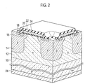
- Fig. 2 shows a schematic bird's-eye view structure of the semiconductor device according to the first embodiment.
- the semiconductor device includes: an n type impurity doped high resistivity first base layer 12; an n type impurity doped drain layer 10 disposed on the back side surface of the first base layer 12; a p type impurity doped second base layer 16 formed on the surface of the first base layer 12; an n type impurity doped source layer 18 formed on the surface of the second base layer 16; a gate insulating film 20 disposed on the surface of both the source layer 18 and the second base layer 16; agate electrode 22 disposed on the gate insulating film 20; a p type impurity doped column layer 14 formed in the first base layer 12 of the lower part of both the second base layer 16 and the source layer 18 by opposing the drain layer 10; a drain electrode 28 disposed in the drain layer 10; and a source electrode 26 disposed on both the source layer 18 and the second base layer 16.
- An interlayer insulating film 24 is disposed on the gate electrode 22. Dashed lines shown
- a trap level is formed locally by performing heavy particle irradiation to the column layer 14.
- P, As, Sb, etc. can be applied as the n type impurity, and B, Al, Ga, etc. can be applied as the p type impurity, for example.
- the above-mentioned impurities can be doped on each layer using diffusion technology or ion implantation technology.
- a silicon dioxide film, a silicon nitride film, a silicon oxynitride film, a hafnium oxide film, an alumina film, a tantalum oxide film, etc. can be applied, for example, as the gate insulating film 20.
- Polysilicon can be applied as the gate electrode 22, and aluminum can be applied to both the drain electrode 28 and the source electrode 26, for example.
- a silicon dioxide film, a silicon nitride film, a tetraethoxy silane (TEOS) film, etc. are applicable, f or example , as the interlayer insulating film 24.
- the schematic planar pattern configuration of the semiconductor device according to the first embodiment shows an example which is disposed being checkered lattice-like on the basis of a rectangular pattern.
- the planar pattern configuration may be disposed being zigzagged checkered lattice-like on the basis of a rectangular pattern, for example.
- the planar pattern configuration may be disposed being zigzagged checkered lattice-like on the basis of a hexagonal pattern, for example.
- the planar pattern configuration is not limited to the rectangle or the hexagon.
- planar pattern configuration is also effective on the basis of circular, an oval figure, a pentagon, a polygon greater than heptagon, etc.
- Fig. 3 and Fig. 4 shows schematically the pattern of semiconductor layers, such as the first base layer 12, the column layer 14, the second base layer 16, and the source layer 18. However, illustrating of the gate electrode 22, the source electrode 26, etc. is omitted.
- Fig. 5 shows an example of a switchingwaveform in the comparative example which does not control life time by the heavy particle irradiation, in the semiconductor device according to the first embodiment.
- the reverse recovery time trr is 160 nsec according to a result shown in Fig. 5 , and is longer than the reverse recovery time being 130 nsec of the conventional example shown in Fig. 12 .
- Fig. 6 shows a schematic cross-section structure for explaining the relation between an irradiation target position and device structure, in the case of performing 3 He ++ ion irradiation (IR) to the semiconductor device according to the first embodiment from the back side surface.
- IR He ++ ion irradiation
- WA denotes the thickness of the drain layer 10 measured from the back side surface of the semiconductor device.
- a coordinate system is defined by applying the direction of the source electrode 26 into a positive direction and applying the direction of the drain layer 10 into a negative direction on the basis of the bottom surface of the column layer 14.
- the irradiation target position can be defined as an attenuation peak position of the range of the heavy ion irradiated from the back side surface of the semiconductor device, and can be indicated on the above-mentioned coordinate system.
- Fig. 7 shows the relation between the saturation current I DSS between the drain and the source and the distance from the bottom surface of the column layer 14 corresponding to the attenuation peak position, in the semiconductor device according to the first embodiment.
- Fig. 7 shows the case of the amount of dosage of 3 He ++ ion is set to 1 ⁇ 10 12 /cm 2 , and is set to 5 ⁇ 10 12 /cm 2 .
- Fig. 8 shows the relation between the reverse recovery time trr and the distance from the bottom surface of the column layer 14 corresponding to the attenuation peak position, in the semiconductor device according to the first embodiment.
- Fig. 8 also shows the case of the amount of dosage of 3 He ++ ion is set to 1 ⁇ 10 12 /cm 2 , and is set to 5 ⁇ 10 12 /cm 2 .
- the value of the saturation current I DSS between the drain and the source tends to decrease as the distance from the bottom surface of the column layer 14 corresponding to the attenuation peak position increases.
- the reverse recovery time trr tends to increase as the distance from the bottom surface of the column layer 14 corresponding to the attenuation peak position increases.
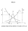
- Fig. 9 shows schematically the relation between: the reverse recovery time trr and the saturation current I DSS between the drain and the source; and the distance from the bottom surface of the column layer 14, in the semiconductor device according to the first embodiment.
- the heavy particle irradiation is performed so that the attenuation peak position of the heavy particle irradiation may be included between: the first position PB obtained from the relation between the distance from the bottom surface of the column layer 14 and the reverse recovery time trr on the basis of the bottom surface of the column layer 14; and the second position PA obtained from the relation between the distance from the bottom surface of the column layer 14 and the saturation current I DSS between the drain and the source, and thereby it can be obtained of the semiconductor device having the reverse recovery time trr shorter than the reverse recovery time to, and having the saturation current I DSS between the drain and the source smaller than the saturation current I 0 between the drain and the source.
- the reverse recovery time trr shorter than the reverse recovery time to, and having the saturation current I DSS between the drain and the source smaller than the saturation current I 0 between the drain and the source.
- the curve D denotes the attenuation peak curve of the heavy particle irradiation for obtaining the semiconductor device having the reverse recovery time trr shorter than the reverse recovery time to, and having the saturation current I DSS between the drain and the source smaller than the saturation current I 0 between the drain and the source.
- the first position PB is the attenuation peak position of the heavy particle irradiation corresponding to the reverse recovery time t 0 .
- the second position PA is the attenuation peak position of the heavy particle irradiation corresponding to the saturation current I 0 between the drain and the source.
- a proton, 3 He ++ , or 4 He ++ can be used for the particle species for performing the heavy particle irradiation, for example.
- 4 He ++ it is preferable to use the drain layer 10 composed of a thin substrate.
- the amount of dosage of the heavy particle irradiation can be set as the scope of 5 ⁇ 10 10 /cm 2 to 5 ⁇ 10 12 /cm 2 , for example.
- Fig. 10 shows the relation between the impurity concentration N, the resistivity p, and sheet resistance R and the distance from the bottom surface of the column layer 14, in the semiconductor device according to the furst embodiment.
- the peak characteristics that the resistivity p and sheet resistance R increase are shown, and the peak characteristics that the impurity concentration N decreases are shown.
- a fabrication method of the semiconductor device includes: the step of forming a high resistivity first base layer 12 of a first conductivity type; the step of forming a drain layer 10 of the first conductivity type on the back side surface of the first base layer 12; the step of forming a second base layer 16 of a second conductivity type on the surface of the first base layer 12; the step of forming a source layer 18 of the first conductivity type on the surface of the second base layer 16; the step of forming a gate insulating film 20 on the surface of both the source layer 18 and the second base layer 16; the step of forming a gate electrode 22 on the gate insulating film 20 ; the step of forming a column layer 14 of the second conductivity type in the first base layer 12 of the lower part of both the second base layer 16 and the source layer 18 by opposing the drain layer 10; the step of forming a drain electrode 28 in the drain layer 10; the step of forming a source electrode in both
- the step of forming the trap level locally includes: the step of determining a first position PB based on the relation between the distance from the bottom surface of the column layer 14 and the reverse recovery time trr on the basis of the bottom surface of the column layer 14; the step of determining a second position PA obtained from the relation between the distance from the bottom surface of the column layer 14 and the saturation current I DSS between the drain and the source; and the step of performing the heavy particle irradiation so that an attenuation peak position may be included between the first position PB and the second position PA.
- the first embodiment it can achieve controlling degradation of both the saturation current I DSS between the drain and the source and the threshold value voltage between the gate and the source, and improving the reverse recovery characteristics of a built-in diode.
- it is possible to reduce the switching power loss, and reduce the diode reverse recovery loss.
- the semiconductor device including the super junction MOS structure where the reverse recovery time trr can be shortened without increasing the leakage current between the drain and the source, and can be provided of the fabrication method for such semiconductor device.
- the semiconductor device according to the present invention is applicable to a bridge circuit, a LCD inverter, a motor, automotive High Intensity Discharge lamp (HID) headlight lighting apparatus, etc. which use a high breakdown voltage MOSFET.
Landscapes
- Insulated Gate Type Field-Effect Transistor (AREA)
- Thin Film Transistor (AREA)
- Chemical & Material Sciences (AREA)
- Composite Materials (AREA)
Abstract
Description
- The present invention relates to a semiconductor device and a fabrication method for such semiconductor device. In particular, the present invention relates to a semiconductor device having a super junction Metal Oxide Semiconductor (MOS) structure, and a fabrication method for such semiconductor device.
- When a MOS Field Effect Transistor (FET) is composed in a bridge circuit, three power loss reductions are required.
- The first power loss is on-state power loss. The on-state power loss is a power loss associated with current flowing through a channel of the MOSFET, and reduction of the on resistance of the MOSFET is required.
- The second power loss is a switching power loss associated with turn-on switching. In order to reduce the switching power loss associated with the turn-on switching, it is required that a turn-on switching time period should be shortened by increasing a gate sensitivity of the MOSFET and reducing an amount of gate charge Qg needed for the turn-on switching.
- The third power loss is a switching power loss associated with the turn-off switching, and is called "through loss". In order to reduce the through loss, it is required that the turn-off switching time should be shortened by shortening Reverse Recovery Time trr of the MOSFET.
- As shown in
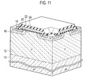
Fig. 11 , a MOSFET of planar structure as a semiconductor device related to a conventional example includes: a high resistivityfirst base layer 12 of a first conductivity type; adrain layer 10 of the first conductivity type formed on the back side surface of thefirst base layer 12; asexond base layer 16 of a second conductivity type formed on the surface of thefirst base layer 12; asource layer 18 of the first conductivity type formed on the surface of thesecond base layer 16; agate insulating film 20 disposed on the surface of both thesource layer 18 and thesecond base layer 16; agate electrode 22 disposed on thegate insulating film 20; and aninterlayer insulating film 24 disposed on thegate electrode 22. InFig. 12 , the illustration is omitted about a drain electrode disposed on thedrain layer 10, and a source electrode disposed on both thesource layer 18 and thesecond base layer 16. -
Fig. 12 shows an example of a switching waveform of the semiconductor device related to the conventional example. - Although the MOSFET including the super junction MOS structure denotes higher performance in respect of both the switching power loss and the on-state power loss compared with the MOSFET of the conventional planar structure, the performance is poor in respect of the through loss.
- That is, the super junction MOSFET includes a column layer of the second conductivity type formed in the
first base layer 12 of the lower part of both thesecond base layer 16 and thesource layer 18 by opposing thedrain layer 10. Accordingly, the on resistance is reduced and the gate sensitivity increases, the amount of gate charge Qg needed for the turn-on switching is reduced, and thereby the turn-on switching time period can be shortened. On the other hand, since the column layer is included, a pn junction area increases, the reverse recovery time trr increases, and thereby the turn-off switching time is increased. Herein, the amount of gate charge Qg is defined as an amount of charge needed for a voltage VGS between the gate and the source in order to reach 10 V, for example. - Generally, a method of using diffusion of a heavy metal and a method of electron irradiation are known as technology for shortening the reverse recovery time trr. According to the above-mentioned methods, although the reverse recovery time trr can be shortened, since the controllability for forming a trap level is wrong, there is a problem that the leakage current between the drain and the source increases.
- Also, in an Insulated Gate Bipolar Transistor (IGBT), it is already proposed about a technology for forming locally a life-time controled layer (for example, refer to Patent Literature 1).
- Moreover, in the IGBT, it is already also disclosed about a technology for irradiating only a predetermined region with an electron ray by using a source electrode formed with aluminum as wiring and using as a mask of electron irradiation (for example, refer to Patent Literature 2).
-
- Patent Literature 1: Japanese Patent Application Laying-Open Publication No.
H10-242165 Fig. 1 , and Pages 3-4) - Patent Literature 2: Japanese Patent Application Laying-Open Publication No.
H10-270451 Fig. 1 , and Page 4) - The object of the present invention is to provide a semiconductor device including a super junction MOS structure where the reverse recovery time trr can be shortened without increasing the leakage current between the drain and the source, and to provide a fabrication method for such semiconductor device.
- According to one aspect of the present invention for achieving the above-mentioned object, it is provided of a semiconductor device comprising: a high resistance first base layer of a first conductivity type; a drain layer of the first conductivity type formed on a back side surface of the first base layer; a second base layer of a second conductivity type formed on a surface of the first base layer; a source layer of the first conductivity type formed on a surface of the second base layer; a gate insulating film disposed on a surface of both the source layer and the second base layer; a gate electrode disposed on the gate insulating film; a column layer of the second conductivity type formed in the first base layer of the lower part of both the second base layer and the source layer by opposing the drain layer; a drain electrode disposed in the drain layer; and a source electrode disposed on both the source layer and the second base layer, wherein heavy particle irradiation is performed to the column layer to form a trap level locally.
- According to another aspect of the present invention, it is provided of a fabrication method for a semiconductor device, the fabrication method comprising: forming a high resistance first base layer of a first conductivity type; forming a drain layer of the first conductivity type on a back side surface of the first base layer; forming a second base layer of a second conductivity type on a surface of the first base layer; forming a source layer of the first conductivity type on a surface of the second base layer; forming a gate insulating film on a surface of both the source layer and the second base layer; forming a gate electrode on the gate insulating film; forming a column layer of the second conductivity type in the first base layer of a lower part of both the second base layer and the source layer by opposing the drain layer; forming a drain electrode in the drain layer,forming a source electrode on both the source layer and the second base layer; and performing heavy particle irradiation to the column layer and forming a trap level locally.
- According to the present invention, it can be provided of the semiconductor device including the super junction MOS structure where the reverse recovery time trr can be shortened without increasing the leakage current between the drain and the source, and can be provided of the fabrication method for such semiconductor device.
-
- [
Fig. 1 ] A schematic cross-sectional configuration diagram of a semiconductor device accoring to a first embodiment of the present invention. - [
Fig. 2 ] A schematic bird's-eye view of the semiconductor device according to the first embodiment of the present invention. - [
Fig. 3 ] A schematic planar pattern configuration diagram of the semiconductor device according to the first embodiment of the present invention. - [
Fig. 4 ] An alternative schematic planar pattern configuration diagram of the semiconductor device according to the first embodiment of the present invention. - [
Fig. 5 ] An example of a switching waveform of a comparative example of the semiconductor device according to the first embodiment of the present invention. - [
Fig. 6 ] The schematic cross-sectional configuration diagram explaining the relation between the irradiation target position and the device structure, in the case of 3He++ ion irradiation to the semiconductor device according to the first embodiment of the present invention from a back side surface. - [
Fig. 7 ] A diagram showing the relation between a saturation current loss between the drain and the source and a distance from a bottom surface of a column layer, in the semiconductor device according to the first embodiment of the present invention. - [
Fig. 8 ] A diagram showing the relation between the reverse recovery time trr and the distance from the bottom surface of the column layer, in the semiconductor device according to the first embodiment of the present invention. - [
Fig. 9 ] A schematic diagram showing the relation between the reverse recovery time trr and the saturation current IDSS between the drain and the source and the distance from the bottom surface of the column layer, in the semiconductor device according to the first embodiment of the present invention. - [
Fig. 10 ] A diagram showing the relation between impurity concentration N, resistivity and sheet resistance R and the distance from the bottom surface of the column layer, in the semiconductor device related to the first embodiment of the present invention. - [
Fig. 11 ] A schematic bird's-eye view of a semiconductor device according to a conventional example. - [
Fig. 12 ] An example of a switching waveform of the semiconductor device according to the conventional example. - Next, embodiments of the present invention will be described with reference to drawings. It explains simple by attaching the same reference numeral as the same block or element to below, in order to avoide duplication of description. However, the drawings are schematic and it should care about differing from an actual thing. Of course, the part from which the relation or ratio between the mutual sizes differ also in mutually drawings may be included.
- The embodiments shown in the following exemplifies the device and method for materializing the technical idea of the present invention, and the embodiments of the present invention does not specify assignment of each component parts, etc. as the following. Various changes can be added to the technical idea of the present invention in scope of claims.
-
Fig. 1 shows a schematic cross-section structure of a semiconductor device according to a first embodiment of the present invention. Moreover,Fig. 2 shows a schematic bird's-eye view structure of the semiconductor device according to the first embodiment. - As shown in
Fig. 1 to Fig. 2 , the semiconductor device according to the first embodiment includes: an n type impurity doped high resistivityfirst base layer 12; an n type impurity dopeddrain layer 10 disposed on the back side surface of thefirst base layer 12; a p type impurity dopedsecond base layer 16 formed on the surface of thefirst base layer 12; an n type impurity dopedsource layer 18 formed on the surface of thesecond base layer 16; agate insulating film 20 disposed on the surface of both thesource layer 18 and thesecond base layer 16;agate electrode 22 disposed on thegate insulating film 20; a p type impurity dopedcolumn layer 14 formed in thefirst base layer 12 of the lower part of both thesecond base layer 16 and thesource layer 18 by opposing thedrain layer 10; adrain electrode 28 disposed in thedrain layer 10; and asource electrode 26 disposed on both thesource layer 18 and thesecond base layer 16. Aninterlayer insulating film 24 is disposed on thegate electrode 22. Dashed lines shown inFig. 1 indicate current which flows between the drain and the source. - In the semiconductor device according to the first embodiment, a trap level is formed locally by performing heavy particle irradiation to the
column layer 14. - P, As, Sb, etc. can be applied as the n type impurity, and B, Al, Ga, etc. can be applied as the p type impurity, for example. The above-mentioned impurities can be doped on each layer using diffusion technology or ion implantation technology.
- A silicon dioxide film, a silicon nitride film, a silicon oxynitride film, a hafnium oxide film, an alumina film, a tantalum oxide film, etc. can be applied, for example, as the gate
insulating film 20. - Polysilicon can be applied as the
gate electrode 22, and aluminum can be applied to both thedrain electrode 28 and thesource electrode 26, for example. - A silicon dioxide film, a silicon nitride film, a tetraethoxy silane (TEOS) film, etc. are applicable, f or example , as the
interlayer insulating film 24. - In the example of
Fig. 2 , the schematic planar pattern configuration of the semiconductor device according to the first embodiment shows an example which is disposed being checkered lattice-like on the basis of a rectangular pattern. On the other hand, as shown inFig. 3 , the planar pattern configuration may be disposed being zigzagged checkered lattice-like on the basis of a rectangular pattern, for example. Alternatively, as shown inFig. 4 , the planar pattern configuration may be disposed being zigzagged checkered lattice-like on the basis of a hexagonal pattern, for example. Moreover, the planar pattern configuration is not limited to the rectangle or the hexagon. That is, the planar pattern configuration is also effective on the basis of circular, an oval figure, a pentagon, a polygon greater than heptagon, etc. Each ofFig. 3 and Fig. 4 shows schematically the pattern of semiconductor layers, such as thefirst base layer 12, thecolumn layer 14, thesecond base layer 16, and thesource layer 18. However, illustrating of thegate electrode 22, thesource electrode 26, etc. is omitted. -
Fig. 5 shows an example of a switchingwaveform in the comparative example which does not control life time by the heavy particle irradiation, in the semiconductor device according to the first embodiment. The reverse recovery time trr is 160 nsec according to a result shown inFig. 5 , and is longer than the reverse recovery time being 130 nsec of the conventional example shown inFig. 12 . -
Fig. 6 shows a schematic cross-section structure for explaining the relation between an irradiation target position and device structure, in the case of performing 3He++ ion irradiation (IR) to the semiconductor device according to the first embodiment from the back side surface. - In
Fig. 6 , WA denotes the thickness of thedrain layer 10 measured from the back side surface of the semiconductor device. Also, WB denotes the distance to the bottom surface of thecolumn layer 14 measured from the back side surface of the semiconductor device. In the example shown inFig. 6 , it is WA=208 µm, and is WB=220 µm. - Moreover, as shown in
Fig. 6 , a coordinate system is defined by applying the direction of thesource electrode 26 into a positive direction and applying the direction of thedrain layer 10 into a negative direction on the basis of the bottom surface of thecolumn layer 14. The irradiation target position can be defined as an attenuation peak position of the range of the heavy ion irradiated from the back side surface of the semiconductor device, and can be indicated on the above-mentioned coordinate system. -
Fig. 7 shows the relation between the saturation current IDSS between the drain and the source and the distance from the bottom surface of thecolumn layer 14 corresponding to the attenuation peak position, in the semiconductor device according to the first embodiment.Fig. 7 shows the case of the amount of dosage of 3He++ ion is set to 1×10¹²/cm2, and is set to 5×10¹²/cm2. - Moreover,
Fig. 8 shows the relation between the reverse recovery time trr and the distance from the bottom surface of thecolumn layer 14 corresponding to the attenuation peak position, in the semiconductor device according to the first embodiment.Fig. 8 also shows the case of the amount of dosage of 3He++ ion is set to 1×10¹²/cm2, and is set to 5×10¹²/cm2 . - As clearly from
Fig. 7 , the value of the saturation current IDSS between the drain and the source tends to decrease as the distance from the bottom surface of thecolumn layer 14 corresponding to the attenuation peak position increases. On the other hand, as clearly fromFig. 8 , the reverse recovery time trr tends to increase as the distance from the bottom surface of thecolumn layer 14 corresponding to the attenuation peak position increases. -
Fig. 9 shows schematically the relation between: the reverse recovery time trr and the saturation current IDSS between the drain and the source; and the distance from the bottom surface of thecolumn layer 14, in the semiconductor device according to the first embodiment. - In the semiconductor device according to the first embodiment, the heavy particle irradiation is performed so that the attenuation peak position of the heavy particle irradiation may be included between: the first position PB obtained from the relation between the distance from the bottom surface of the
column layer 14 and the reverse recovery time trr on the basis of the bottom surface of thecolumn layer 14; and the second position PA obtained from the relation between the distance from the bottom surface of thecolumn layer 14 and the saturation current IDSS between the drain and the source, and thereby it can be obtained of the semiconductor device having the reverse recovery time trr shorter than the reverse recovery time to, and having the saturation current IDSS between the drain and the source smaller than the saturation current I0 between the drain and the source. InFig. 9 , the curve D denotes the attenuation peak curve of the heavy particle irradiation for obtaining the semiconductor device having the reverse recovery time trr shorter than the reverse recovery time to, and having the saturation current IDSS between the drain and the source smaller than the saturation current I0 between the drain and the source. - Here, the first position PB is the attenuation peak position of the heavy particle irradiation corresponding to the reverse recovery time t0. Moreover, the second position PA is the attenuation peak position of the heavy particle irradiation corresponding to the saturation current I0 between the drain and the source. Forexample, when the reverse recovery time t0 is set to 80 nsec and the saturation current I0 between the drain and source is set to 1 µA, it can be obtained of the semiconductor device whose the reverse recovery time trr<t0=80 nsec, and the saturation current between the drain and the source IDSS <I0=1 µA.
- Here, a proton, 3He++, or 4He++ can be used for the particle species for performing the heavy particle irradiation, for example. When using 4He++ as the particle species for performing the heavy particle irradiation, it is preferable to use the
drain layer 10 composed of a thin substrate. - The amount of dosage of the heavy particle irradiation can be set as the scope of 5×10¹⁰/cm2 to 5×10¹²/cm2, for example.
-
Fig. 10 shows the relation between the impurity concentration N, the resistivity p, and sheet resistance R and the distance from the bottom surface of thecolumn layer 14, in the semiconductor device according to the furst embodiment. Corresponding to the tendency of the attenuation peak curve of heavy particle irradiation, the peak characteristics that the resistivity p and sheet resistance R increase are shown, and the peak characteristics that the impurity concentration N decreases are shown. - As shown in
Fig. 1 to Fig. 2 , a fabrication method of the semiconductor device according to the first embodiment includes: the step of forming a high resistivityfirst base layer 12 of a first conductivity type; the step of forming adrain layer 10 of the first conductivity type on the back side surface of thefirst base layer 12; the step of forming asecond base layer 16 of a second conductivity type on the surface of thefirst base layer 12; the step of forming asource layer 18 of the first conductivity type on the surface of thesecond base layer 16; the step of forming agate insulating film 20 on the surface of both thesource layer 18 and thesecond base layer 16; the step of forming agate electrode 22 on thegate insulating film 20 ; the step of forming acolumn layer 14 of the second conductivity type in thefirst base layer 12 of the lower part of both thesecond base layer 16 and thesource layer 18 by opposing thedrain layer 10; the step of forming adrain electrode 28 in thedrain layer 10; the step of forming a source electrode in both the source layer and the second base layer; and the step of performing heavy particle irradiation to thecolumn layer 14 and forming a trap level locally. - As shown in
Fig. 9 , the step of forming the trap level locally includes: the step of determining a first position PB based on the relation between the distance from the bottom surface of thecolumn layer 14 and the reverse recovery time trr on the basis of the bottom surface of thecolumn layer 14; the step of determining a second position PA obtained from the relation between the distance from the bottom surface of thecolumn layer 14 and the saturation current IDSS between the drain and the source; and the step of performing the heavy particle irradiation so that an attenuation peak position may be included between the first position PB and the second position PA. - According to the first embodiment, it can achieve controlling degradation of both the saturation current IDSS between the drain and the source and the threshold value voltage between the gate and the source, and improving the reverse recovery characteristics of a built-in diode. Thus, it is possible to reduce the switching power loss, and reduce the diode reverse recovery loss.
- According to the first embodiment, it can be provided of the semiconductor device including the super junction MOS structure where the reverse recovery time trr can be shortened without increasing the leakage current between the drain and the source, and can be provided of the fabrication method for such semiconductor device.
- The present invention has been described by the first embodiment, as a disclosure including associated description and drawings to be construed as illustrative, not restrictive. With the disclosure, a person skilled in the art might easily think up alternative embodiments, embodiment examples, or application techniques.
- Thus, the present invention includes various embodiments etc. which have not been described in this specification.
- The semiconductor device according to the present invention is applicable to a bridge circuit, a LCD inverter, a motor, automotive High Intensity Discharge lamp (HID) headlight lighting apparatus, etc. which use a high breakdown voltage MOSFET.
-
- 10:
- Drain layer;
- 12:
- First base layer;
- 14:
- Column layer;
- 16:
- Second base layer;
- 18:
- Source layer;
- 20:
- Gate insulating film;
- 22:
- Gate electrode;
- 24:
- Interlayer insulating film;
- 26:
- Source electrode; and
- 28:
- Drain electrode.
Claims (9)
- A semiconductor device comprising:a high resistance first base layer of a first conductivity type;a drain layer of the first conductivity type formed on a back side surface of the first base layer;a second base layer of a second conductivity type formed on a surface of the first base layer;a source layer of the first conductivity type formed on a surface of the second base layer;a gate insulating film disposed on a surface of both the source layer and the second base layer;a gate electrode disposed on the gate insulating film;a column layer of the second conductivity type formed in the first base layer of the lower part of both the second base layer and the source layer by opposing the drain layer;a drain electrode disposed in the drain layer; anda source electrode disposed on both the source layer and the second base layer, whereinheavy particle irradiation is performed to the column layer to form a trap level locally.
- The semiconductor device according to claim 1, wherein an attenuation peak position of an ion irradiation is included between: a first position obtained from a relation between the distance from a bottom surface of the column layer and reverse recovery time; and a second position obtained from a relation between the distance from the bottom surface of column layer and a saturation current between the drain and the source, on the basis of the bottom surface of the column layer.
- The semiconductor device according to claim 1 or 2, wherein the particle species for performing the heavy particle irradiation is one of a proton, 3He++, and 4He++.
- The semiconductor device according to any one of claims 1 to 3, wherein an amount of dosage of the heavy particle irradiation is 5×10¹⁰/cm2 to 5×10¹²/cm2.
- The semiconductor device according to any one of claims 1 to 4, wherein a planar pattern on the basis of one of a rectangle and a hexagon is disposed being checkered lattice-like or zigzagged checkered lattice-like, in the first base layer, the second base layer, and the source layer.
- A fabrication method for a semiconductor device, the fabrication method comprising:forming a high resistance first base layer of a first conductivity type;forming a drain layer of the first conductivity type on a back side surface of the first base layer;forming a second base layer of a second conductivity type on a surface of the first base layer;forming a source layer of the first conductivity type on a surface of the second base layer;forming a gate insulating film on a surface of both the source layer and the second base layer;forming a gate electrode on the gate insulating film;forming a column layer of the second conductivity type in the first base layer of a lower part of both the second base layer and the source layer by opposing the drain layer;forming a drain electrode in the drain layer,forming a source electrode on both the source layer and the second base layer; andperforming heavy particle irradiation to the column layer and forming a trap level locally.
- The fabrication method for the semiconductor device according to claim 6, wherein the step of forming the trap level locally includes:determining a first position based on a relation between the distance from a bottom surface of the column layer and reverse recovery time, on the basis of the bottom surface of the column layer;determining a second position obtained from a relation between the distance from the bottom surface of the column layer and a saturation current between the drain and the source; andperforming the heavy particle irradiation so that an attenuation peak position is included between the first position and the second position.
- The fabrication method for the semiconductor device according to claims 6 or 7, wherein the particle species for performing the heavy particle irradiation is one of a proton, 3He++, and 4He++.
- The fabrication method for the semiconductor device according to any one of claims 6 to 8, wherein an amount of dosage of the heavy particle irradiation is 5×10¹⁰/cm2 to 5×10¹²/cm2.
Applications Claiming Priority (2)
| Application Number | Priority Date | Filing Date | Title |
|---|---|---|---|
| JP2008223370 | 2008-09-01 | ||
| PCT/JP2009/065171 WO2010024433A1 (en) | 2008-09-01 | 2009-08-31 | Semiconductor device and manufacturing method thereof |
Publications (2)
| Publication Number | Publication Date |
|---|---|
| EP2330617A1 true EP2330617A1 (en) | 2011-06-08 |
| EP2330617A4 EP2330617A4 (en) | 2012-01-25 |
Family
ID=41721592
Family Applications (1)
| Application Number | Title | Priority Date | Filing Date |
|---|---|---|---|
| EP09810077A Withdrawn EP2330617A4 (en) | 2008-09-01 | 2009-08-31 | SEMICONDUCTOR DEVICE AND METHOD FOR MANUFACTURING THE SAME |
Country Status (7)
| Country | Link |
|---|---|
| US (6) | US8492829B2 (en) |
| EP (1) | EP2330617A4 (en) |
| JP (4) | JP5723595B2 (en) |
| KR (1) | KR101614565B1 (en) |
| CN (1) | CN102138206B (en) |
| TW (1) | TWI470799B (en) |
| WO (1) | WO2010024433A1 (en) |
Families Citing this family (23)
| Publication number | Priority date | Publication date | Assignee | Title |
|---|---|---|---|---|
| US8492829B2 (en) | 2008-09-01 | 2013-07-23 | Rohm Co., Ltd. | Semiconductor device having super junction metal oxide semiconductor structure and fabrication method for the same |
| JP5748476B2 (en) | 2010-12-28 | 2015-07-15 | ローム株式会社 | Semiconductor device and manufacturing method thereof |
| JP5586546B2 (en) * | 2011-03-23 | 2014-09-10 | 株式会社東芝 | Semiconductor device |
| JP6037495B2 (en) * | 2011-10-17 | 2016-12-07 | ローム株式会社 | Semiconductor device and manufacturing method thereof |
| CN103325825B (en) * | 2012-03-20 | 2016-01-27 | 宁波敏泰光电科技有限公司 | Super node MOSFET |
| JP6263966B2 (en) * | 2012-12-12 | 2018-01-24 | 富士電機株式会社 | Semiconductor device |
| JP6135178B2 (en) | 2013-02-25 | 2017-05-31 | 富士電機株式会社 | Manufacturing method of super junction semiconductor device |
| JP6221436B2 (en) | 2013-07-10 | 2017-11-01 | 富士電機株式会社 | Superjunction MOSFET, manufacturing method thereof, and composite semiconductor device in which diodes are connected in parallel |
| JP6075458B2 (en) | 2013-09-18 | 2017-02-08 | 富士電機株式会社 | Semiconductor device and manufacturing method thereof |
| US9472456B2 (en) * | 2013-12-24 | 2016-10-18 | Intel Corporation | Technology for selectively etching titanium and titanium nitride in the presence of other materials |
| JP6605887B2 (en) * | 2015-09-07 | 2019-11-13 | 日立ジョンソンコントロールズ空調株式会社 | DC power supply device and air conditioner equipped with the same |
| JP6652802B2 (en) | 2015-09-15 | 2020-02-26 | ローム株式会社 | Semiconductor device and inverter device including the semiconductor device |
| CN105161491B (en) * | 2015-09-22 | 2019-03-15 | 苏州东微半导体有限公司 | A kind of integrated gate driving power device and preparation method thereof |
| JP2017183419A (en) * | 2016-03-29 | 2017-10-05 | ローム株式会社 | Semiconductor device |
| JP7238186B2 (en) * | 2016-06-28 | 2023-03-13 | 日立ジョンソンコントロールズ空調株式会社 | Power conversion device and air conditioner provided with the same |
| CN106887464B (en) * | 2017-01-04 | 2019-12-06 | 上海华虹宏力半导体制造有限公司 | Super junction device and manufacturing method thereof |
| JP6847681B2 (en) | 2017-01-27 | 2021-03-24 | ローム株式会社 | Semiconductor device |
| US10186586B1 (en) * | 2017-09-26 | 2019-01-22 | Sanken Electric Co., Ltd. | Semiconductor device and method for forming the semiconductor device |
| WO2019087341A1 (en) | 2017-11-01 | 2019-05-09 | 新電元工業株式会社 | Semiconductor device and method for manufacturing semiconductor device |
| WO2019130513A1 (en) | 2017-12-27 | 2019-07-04 | 新電元工業株式会社 | Mosfet, method for manufacturing mosfet, and power conversion circuit |
| JP7007971B2 (en) | 2018-03-29 | 2022-01-25 | ローム株式会社 | Semiconductor device |
| JP7281589B2 (en) * | 2019-10-16 | 2023-05-25 | 日立ジョンソンコントロールズ空調株式会社 | DC power supply device and air conditioner equipped with the same |
| JP6873207B2 (en) * | 2019-10-16 | 2021-05-19 | 日立ジョンソンコントロールズ空調株式会社 | DC power supply and air conditioner equipped with it |
Family Cites Families (48)
| Publication number | Priority date | Publication date | Assignee | Title |
|---|---|---|---|---|
| US4053925A (en) * | 1975-08-07 | 1977-10-11 | Ibm Corporation | Method and structure for controllng carrier lifetime in semiconductor devices |
| US4762802A (en) * | 1984-11-09 | 1988-08-09 | American Telephone And Telegraph Company At&T, Bell Laboratories | Method for preventing latchup in CMOS devices |
| JPS62219664A (en) * | 1986-03-20 | 1987-09-26 | Hitachi Ltd | Manufacture of mos type semiconductor element |
| JPS62298120A (en) | 1986-06-18 | 1987-12-25 | Hitachi Ltd | Semicionductor device and manufacture thereof |
| JPS63115383A (en) * | 1986-11-04 | 1988-05-19 | Matsushita Electronics Corp | Manufacture of field-effect trasistor |
| JP3034895B2 (en) | 1990-03-08 | 2000-04-17 | 株式会社日立製作所 | Power converter system |
| JPH03259537A (en) * | 1990-03-09 | 1991-11-19 | Hitachi Ltd | Semiconductor device and manufacture thereof |
| JPH03263376A (en) * | 1990-03-13 | 1991-11-22 | Mitsubishi Electric Corp | Field-effect semiconductor device |
| JP3081739B2 (en) * | 1992-10-20 | 2000-08-28 | 三菱電機株式会社 | Insulated gate semiconductor device and method of manufacturing the same |
| DE69430913D1 (en) * | 1994-07-25 | 2002-08-08 | Cons Ric Microelettronica | Procedure for the local reduction of the carrier lifetime |
| JP3259537B2 (en) | 1994-08-29 | 2002-02-25 | 松下電器産業株式会社 | Method for manufacturing semiconductor device |
| JP2883017B2 (en) * | 1995-02-20 | 1999-04-19 | ローム株式会社 | Semiconductor device and manufacturing method thereof |
| JPH09121052A (en) | 1995-08-21 | 1997-05-06 | Fuji Electric Co Ltd | Semiconductor device and manufacturing method thereof |
| US5759904A (en) * | 1996-11-06 | 1998-06-02 | Southwest Research Institute | Suppression of transient enhanced diffusion in ion implanted silicon |
| JPH10150208A (en) * | 1996-11-15 | 1998-06-02 | Toshiba Corp | Method for manufacturing semiconductor device |
| JP3622405B2 (en) | 1997-02-28 | 2005-02-23 | 株式会社日立製作所 | Semiconductor switching element and IGBT module |
| JPH10270451A (en) | 1997-03-25 | 1998-10-09 | Rohm Co Ltd | Semiconductor device and manufacturing method thereof |
| DE19730759C1 (en) * | 1997-07-17 | 1998-09-03 | Siemens Ag | Vertical power MOSFET |
| DE19830332C2 (en) * | 1998-07-07 | 2003-04-17 | Infineon Technologies Ag | Vertical semiconductor device with reduced electrical surface field |
| JP3507732B2 (en) * | 1999-09-30 | 2004-03-15 | 株式会社東芝 | Semiconductor device |
| JP4653273B2 (en) * | 1999-11-05 | 2011-03-16 | 富士電機システムズ株式会社 | Semiconductor device and manufacturing method thereof |
| US6709955B2 (en) * | 2000-04-17 | 2004-03-23 | Stmicroelectronics S.R.L. | Method of fabricating electronic devices integrated in semiconductor substrates provided with gettering sites, and a device fabricated by the method |
| US6509240B2 (en) * | 2000-05-15 | 2003-01-21 | International Rectifier Corporation | Angle implant process for cellular deep trench sidewall doping |
| JP2002093813A (en) * | 2000-09-13 | 2002-03-29 | Toyota Motor Corp | Method for manufacturing semiconductor device |
| DE10120656C2 (en) * | 2001-04-27 | 2003-07-10 | Infineon Technologies Ag | Semiconductor component with increased avalanche strength |
| JP2003101022A (en) | 2001-09-27 | 2003-04-04 | Toshiba Corp | Power semiconductor device |
| DE10137676B4 (en) * | 2001-08-01 | 2007-08-23 | Infineon Technologies Ag | ZVS bridge circuit for relieved switching |
| US20030030051A1 (en) * | 2001-08-09 | 2003-02-13 | International Rectifier Corporation | Superjunction device with improved avalanche capability and breakdown voltage |
| US6686244B2 (en) * | 2002-03-21 | 2004-02-03 | General Semiconductor, Inc. | Power semiconductor device having a voltage sustaining region that includes doped columns formed with a single ion implantation step |
| JP3952452B2 (en) * | 2002-03-25 | 2007-08-01 | 新電元工業株式会社 | Manufacturing method of semiconductor device |
| JP3979258B2 (en) * | 2002-05-21 | 2007-09-19 | 富士電機デバイステクノロジー株式会社 | MIS semiconductor device and manufacturing method thereof |
| JP3925319B2 (en) * | 2002-06-14 | 2007-06-06 | 富士電機デバイステクノロジー株式会社 | Semiconductor element |
| DE10243758A1 (en) * | 2002-09-20 | 2004-04-01 | eupec Europäische Gesellschaft für Leistungshalbleiter mbH | Method for producing a buried stop zone in a semiconductor component and semiconductor component with a buried stop zone |
| US6838321B2 (en) * | 2002-09-26 | 2005-01-04 | Mitsubishi Denki Kabushiki Kaisha | Semiconductor substrate with defects reduced or removed and method of manufacturing the same, and semiconductor device capable of bidirectionally retaining breakdown voltage and method of manufacturing the same |
| US7166890B2 (en) * | 2003-10-21 | 2007-01-23 | Srikant Sridevan | Superjunction device with improved ruggedness |
| JP4940535B2 (en) * | 2004-01-08 | 2012-05-30 | 株式会社豊田中央研究所 | Semiconductor device |
| JP4832731B2 (en) | 2004-07-07 | 2011-12-07 | 株式会社東芝 | Power semiconductor device |
| JP4843253B2 (en) * | 2005-05-23 | 2011-12-21 | 株式会社東芝 | Power semiconductor device |
| JP4996848B2 (en) | 2005-11-30 | 2012-08-08 | 株式会社東芝 | Semiconductor device |
| DE502007003501D1 (en) * | 2006-01-20 | 2010-06-02 | Infineon Technologies Austria | NDEN SEMICONDUCTOR WAFERS AND SEMICONDUCTOR ELEMENT |
| JP2008124300A (en) | 2006-11-14 | 2008-05-29 | Rohm Co Ltd | Semiconductor device and electric circuit using the same |
| JP4412344B2 (en) | 2007-04-03 | 2010-02-10 | 株式会社デンソー | Semiconductor device and manufacturing method thereof |
| DE102007022533B4 (en) * | 2007-05-14 | 2014-04-30 | Infineon Technologies Ag | Method for producing a semiconductor element and semiconductor element |
| US8492829B2 (en) * | 2008-09-01 | 2013-07-23 | Rohm Co., Ltd. | Semiconductor device having super junction metal oxide semiconductor structure and fabrication method for the same |
| JP5748476B2 (en) * | 2010-12-28 | 2015-07-15 | ローム株式会社 | Semiconductor device and manufacturing method thereof |
| JP6135178B2 (en) * | 2013-02-25 | 2017-05-31 | 富士電機株式会社 | Manufacturing method of super junction semiconductor device |
| JP6234696B2 (en) * | 2013-04-16 | 2017-11-22 | ローム株式会社 | Semiconductor device |
| JP6611532B2 (en) * | 2015-09-17 | 2019-11-27 | ローム株式会社 | Semiconductor device and manufacturing method of semiconductor device |
-
2009
- 2009-08-31 US US12/737,912 patent/US8492829B2/en active Active
- 2009-08-31 CN CN200980133767.9A patent/CN102138206B/en active Active
- 2009-08-31 JP JP2010526808A patent/JP5723595B2/en active Active
- 2009-08-31 EP EP09810077A patent/EP2330617A4/en not_active Withdrawn
- 2009-08-31 WO PCT/JP2009/065171 patent/WO2010024433A1/en not_active Ceased
- 2009-08-31 KR KR1020117007467A patent/KR101614565B1/en not_active Expired - Fee Related
- 2009-09-01 TW TW98129401A patent/TWI470799B/en not_active IP Right Cessation
-
2013
- 2013-06-20 US US13/922,441 patent/US8802548B2/en active Active
-
2014
- 2014-07-01 US US14/320,671 patent/US9385217B2/en active Active
-
2015
- 2015-03-24 JP JP2015061288A patent/JP6243370B2/en active Active
-
2016
- 2016-06-04 US US15/173,652 patent/US9755065B2/en active Active
-
2017
- 2017-08-14 US US15/677,003 patent/US10217856B2/en active Active
- 2017-09-01 JP JP2017168375A patent/JP6557304B2/en active Active
-
2019
- 2019-01-11 US US16/245,681 patent/US10672900B2/en active Active
- 2019-06-11 JP JP2019108642A patent/JP6731522B2/en active Active
Also Published As
| Publication number | Publication date |
|---|---|
| JP2015135987A (en) | 2015-07-27 |
| US20180012987A1 (en) | 2018-01-11 |
| KR101614565B1 (en) | 2016-04-21 |
| US20160284835A1 (en) | 2016-09-29 |
| JP5723595B2 (en) | 2015-05-27 |
| JP2019145849A (en) | 2019-08-29 |
| US8802548B2 (en) | 2014-08-12 |
| JPWO2010024433A1 (en) | 2012-01-26 |
| US10217856B2 (en) | 2019-02-26 |
| US20110147829A1 (en) | 2011-06-23 |
| CN102138206A (en) | 2011-07-27 |
| US20190148536A1 (en) | 2019-05-16 |
| JP6243370B2 (en) | 2017-12-06 |
| TWI470799B (en) | 2015-01-21 |
| JP2017228793A (en) | 2017-12-28 |
| US9755065B2 (en) | 2017-09-05 |
| WO2010024433A1 (en) | 2010-03-04 |
| US9385217B2 (en) | 2016-07-05 |
| EP2330617A4 (en) | 2012-01-25 |
| US8492829B2 (en) | 2013-07-23 |
| US20140312411A1 (en) | 2014-10-23 |
| JP6557304B2 (en) | 2019-08-07 |
| JP6731522B2 (en) | 2020-07-29 |
| KR20110069039A (en) | 2011-06-22 |
| US20130302957A1 (en) | 2013-11-14 |
| CN102138206B (en) | 2014-03-12 |
| TW201011917A (en) | 2010-03-16 |
| US10672900B2 (en) | 2020-06-02 |
Similar Documents
| Publication | Publication Date | Title |
|---|---|---|
| US10672900B2 (en) | Semiconductor device having super junction metal oxide semiconductor structure and fabrication method for the same | |
| US6246092B1 (en) | High breakdown voltage MOS semiconductor apparatus | |
| US8294206B2 (en) | Integrated circuit device and method for its production | |
| US20140209972A1 (en) | Semiconductor device | |
| US20150054025A1 (en) | Semiconductor device and semiconductor device manufacturing method | |
| US9887279B2 (en) | Semiconductor device and inverter including the semiconductor device | |
| US9799763B2 (en) | Method and structure for reducing switching power losses | |
| US5940721A (en) | Termination structure for semiconductor devices and process for manufacture thereof | |
| EP4120360A1 (en) | Power semiconductor device | |
| JPH09102605A (en) | Accumulation mode field effect transistor | |
| US11394194B2 (en) | Semiconductor device with surge current protection | |
| JP2014165293A (en) | Field-MOSFET AND MANUFACTURING METHOD THEREFOR | |
| US7253030B2 (en) | Method of fabricating high-voltage CMOS device | |
| Vashchenko et al. | On chip ESD protection of 600V voltage node | |
| KR100592225B1 (en) | High voltage device formation method using double epitaxial growth | |
| CN118136670A (en) | A power semiconductor device including a Schottky contact super barrier rectifier | |
| JP2007134421A (en) | Vertical semiconductor device such as power MOSFET and IGBT, and manufacturing method thereof | |
| CN101728430A (en) | High voltage metal oxide semiconductor assembly and manufacturing method thereof |
Legal Events
| Date | Code | Title | Description |
|---|---|---|---|
| PUAI | Public reference made under article 153(3) epc to a published international application that has entered the european phase |
Free format text: ORIGINAL CODE: 0009012 |
|
| 17P | Request for examination filed |
Effective date: 20110325 |
|
| AK | Designated contracting states |
Kind code of ref document: A1 Designated state(s): AT BE BG CH CY CZ DE DK EE ES FI FR GB GR HR HU IE IS IT LI LT LU LV MC MK MT NL NO PL PT RO SE SI SK SM TR |
|
| AX | Request for extension of the european patent |
Extension state: AL BA RS |
|
| DAX | Request for extension of the european patent (deleted) | ||
| A4 | Supplementary search report drawn up and despatched |
Effective date: 20111222 |
|
| RIC1 | Information provided on ipc code assigned before grant |
Ipc: H01L 29/78 20060101ALI20111216BHEP Ipc: H01L 21/336 20060101AFI20111216BHEP |
|
| STAA | Information on the status of an ep patent application or granted ep patent |
Free format text: STATUS: THE APPLICATION IS DEEMED TO BE WITHDRAWN |
|
| 18D | Application deemed to be withdrawn |
Effective date: 20120721 |