JP2017183419A - Semiconductor device - Google Patents
Semiconductor device Download PDFInfo
- Publication number
- JP2017183419A JP2017183419A JP2016066392A JP2016066392A JP2017183419A JP 2017183419 A JP2017183419 A JP 2017183419A JP 2016066392 A JP2016066392 A JP 2016066392A JP 2016066392 A JP2016066392 A JP 2016066392A JP 2017183419 A JP2017183419 A JP 2017183419A
- Authority
- JP
- Japan
- Prior art keywords
- type
- region
- layer
- semiconductor device
- pillar
- Prior art date
- Legal status (The legal status is an assumption and is not a legal conclusion. Google has not performed a legal analysis and makes no representation as to the accuracy of the status listed.)
- Pending
Links
- 239000004065 semiconductor Substances 0.000 title claims abstract description 142
- 210000000746 body region Anatomy 0.000 claims abstract description 57
- 230000005684 electric field Effects 0.000 claims abstract description 34
- 239000012141 concentrate Substances 0.000 claims abstract 2
- 239000012535 impurity Substances 0.000 claims description 32
- 239000002245 particle Substances 0.000 claims description 16
- YZCKVEUIGOORGS-OUBTZVSYSA-N Deuterium Chemical compound [2H] YZCKVEUIGOORGS-OUBTZVSYSA-N 0.000 claims description 4
- 229910052805 deuterium Inorganic materials 0.000 claims description 4
- 238000011084 recovery Methods 0.000 abstract description 28
- 238000009413 insulation Methods 0.000 abstract 1
- 239000010410 layer Substances 0.000 description 188
- 238000010586 diagram Methods 0.000 description 23
- 239000000758 substrate Substances 0.000 description 22
- 150000002500 ions Chemical class 0.000 description 12
- 230000003071 parasitic effect Effects 0.000 description 10
- 238000004519 manufacturing process Methods 0.000 description 9
- 238000000137 annealing Methods 0.000 description 8
- 239000011229 interlayer Substances 0.000 description 8
- 238000000034 method Methods 0.000 description 7
- 238000010438 heat treatment Methods 0.000 description 6
- 239000000969 carrier Substances 0.000 description 5
- 239000013078 crystal Substances 0.000 description 4
- 238000000227 grinding Methods 0.000 description 4
- 230000006798 recombination Effects 0.000 description 4
- XUIMIQQOPSSXEZ-UHFFFAOYSA-N Silicon Chemical compound [Si] XUIMIQQOPSSXEZ-UHFFFAOYSA-N 0.000 description 3
- 238000005275 alloying Methods 0.000 description 3
- 229910052782 aluminium Inorganic materials 0.000 description 3
- XAGFODPZIPBFFR-UHFFFAOYSA-N aluminium Chemical compound [Al] XAGFODPZIPBFFR-UHFFFAOYSA-N 0.000 description 3
- 230000015556 catabolic process Effects 0.000 description 3
- 230000007423 decrease Effects 0.000 description 3
- 238000009826 distribution Methods 0.000 description 3
- 230000000694 effects Effects 0.000 description 3
- 238000005530 etching Methods 0.000 description 3
- 230000001678 irradiating effect Effects 0.000 description 3
- 229910052751 metal Inorganic materials 0.000 description 3
- 239000002184 metal Substances 0.000 description 3
- 229920002120 photoresistant polymer Polymers 0.000 description 3
- 229910021420 polycrystalline silicon Inorganic materials 0.000 description 3
- 229920005591 polysilicon Polymers 0.000 description 3
- 238000004904 shortening Methods 0.000 description 3
- 229910052710 silicon Inorganic materials 0.000 description 3
- 239000010703 silicon Substances 0.000 description 3
- 229910052581 Si3N4 Inorganic materials 0.000 description 2
- VYPSYNLAJGMNEJ-UHFFFAOYSA-N Silicium dioxide Chemical compound O=[Si]=O VYPSYNLAJGMNEJ-UHFFFAOYSA-N 0.000 description 2
- BOTDANWDWHJENH-UHFFFAOYSA-N Tetraethyl orthosilicate Chemical compound CCO[Si](OCC)(OCC)OCC BOTDANWDWHJENH-UHFFFAOYSA-N 0.000 description 2
- 230000007547 defect Effects 0.000 description 2
- 238000009792 diffusion process Methods 0.000 description 2
- 229910052734 helium Inorganic materials 0.000 description 2
- 239000001307 helium Substances 0.000 description 2
- SWQJXJOGLNCZEY-UHFFFAOYSA-N helium atom Chemical compound [He] SWQJXJOGLNCZEY-UHFFFAOYSA-N 0.000 description 2
- 238000000206 photolithography Methods 0.000 description 2
- 238000005215 recombination Methods 0.000 description 2
- HQVNEWCFYHHQES-UHFFFAOYSA-N silicon nitride Chemical compound N12[Si]34N5[Si]62N3[Si]51N64 HQVNEWCFYHHQES-UHFFFAOYSA-N 0.000 description 2
- 229910052814 silicon oxide Inorganic materials 0.000 description 2
- 238000004088 simulation Methods 0.000 description 2
- ZOXJGFHDIHLPTG-UHFFFAOYSA-N Boron Chemical compound [B] ZOXJGFHDIHLPTG-UHFFFAOYSA-N 0.000 description 1
- GYHNNYVSQQEPJS-UHFFFAOYSA-N Gallium Chemical compound [Ga] GYHNNYVSQQEPJS-UHFFFAOYSA-N 0.000 description 1
- OAICVXFJPJFONN-UHFFFAOYSA-N Phosphorus Chemical compound [P] OAICVXFJPJFONN-UHFFFAOYSA-N 0.000 description 1
- PNEYBMLMFCGWSK-UHFFFAOYSA-N aluminium oxide Inorganic materials [O-2].[O-2].[O-2].[Al+3].[Al+3] PNEYBMLMFCGWSK-UHFFFAOYSA-N 0.000 description 1
- 229910052787 antimony Inorganic materials 0.000 description 1
- WATWJIUSRGPENY-UHFFFAOYSA-N antimony atom Chemical compound [Sb] WATWJIUSRGPENY-UHFFFAOYSA-N 0.000 description 1
- 229910052785 arsenic Inorganic materials 0.000 description 1
- RQNWIZPPADIBDY-UHFFFAOYSA-N arsenic atom Chemical compound [As] RQNWIZPPADIBDY-UHFFFAOYSA-N 0.000 description 1
- 238000004380 ashing Methods 0.000 description 1
- 230000015572 biosynthetic process Effects 0.000 description 1
- 229910052796 boron Inorganic materials 0.000 description 1
- 230000005465 channeling Effects 0.000 description 1
- 230000005669 field effect Effects 0.000 description 1
- 229910052733 gallium Inorganic materials 0.000 description 1
- 229910000449 hafnium oxide Inorganic materials 0.000 description 1
- WIHZLLGSGQNAGK-UHFFFAOYSA-N hafnium(4+);oxygen(2-) Chemical compound [O-2].[O-2].[Hf+4] WIHZLLGSGQNAGK-UHFFFAOYSA-N 0.000 description 1
- 238000002513 implantation Methods 0.000 description 1
- 230000001939 inductive effect Effects 0.000 description 1
- 239000011810 insulating material Substances 0.000 description 1
- 238000005468 ion implantation Methods 0.000 description 1
- 230000001788 irregular Effects 0.000 description 1
- 230000007257 malfunction Effects 0.000 description 1
- 238000002844 melting Methods 0.000 description 1
- 230000008018 melting Effects 0.000 description 1
- 229910044991 metal oxide Inorganic materials 0.000 description 1
- 150000004706 metal oxides Chemical class 0.000 description 1
- 230000003647 oxidation Effects 0.000 description 1
- 238000007254 oxidation reaction Methods 0.000 description 1
- BPUBBGLMJRNUCC-UHFFFAOYSA-N oxygen(2-);tantalum(5+) Chemical compound [O-2].[O-2].[O-2].[O-2].[O-2].[Ta+5].[Ta+5] BPUBBGLMJRNUCC-UHFFFAOYSA-N 0.000 description 1
- 230000000149 penetrating effect Effects 0.000 description 1
- 230000002093 peripheral effect Effects 0.000 description 1
- 229910052698 phosphorus Inorganic materials 0.000 description 1
- 239000011574 phosphorus Substances 0.000 description 1
- 239000002344 surface layer Substances 0.000 description 1
- 229910001936 tantalum oxide Inorganic materials 0.000 description 1
Images


Classifications
-
- H—ELECTRICITY
- H01—ELECTRIC ELEMENTS
- H01L—SEMICONDUCTOR DEVICES NOT COVERED BY CLASS H10
- H01L29/00—Semiconductor devices specially adapted for rectifying, amplifying, oscillating or switching and having potential barriers; Capacitors or resistors having potential barriers, e.g. a PN-junction depletion layer or carrier concentration layer; Details of semiconductor bodies or of electrodes thereof ; Multistep manufacturing processes therefor
- H01L29/02—Semiconductor bodies ; Multistep manufacturing processes therefor
- H01L29/06—Semiconductor bodies ; Multistep manufacturing processes therefor characterised by their shape; characterised by the shapes, relative sizes, or dispositions of the semiconductor regions ; characterised by the concentration or distribution of impurities within semiconductor regions
- H01L29/10—Semiconductor bodies ; Multistep manufacturing processes therefor characterised by their shape; characterised by the shapes, relative sizes, or dispositions of the semiconductor regions ; characterised by the concentration or distribution of impurities within semiconductor regions with semiconductor regions connected to an electrode not carrying current to be rectified, amplified or switched and such electrode being part of a semiconductor device which comprises three or more electrodes
- H01L29/1095—Body region, i.e. base region, of DMOS transistors or IGBTs
-
- H—ELECTRICITY
- H01—ELECTRIC ELEMENTS
- H01L—SEMICONDUCTOR DEVICES NOT COVERED BY CLASS H10
- H01L29/00—Semiconductor devices specially adapted for rectifying, amplifying, oscillating or switching and having potential barriers; Capacitors or resistors having potential barriers, e.g. a PN-junction depletion layer or carrier concentration layer; Details of semiconductor bodies or of electrodes thereof ; Multistep manufacturing processes therefor
- H01L29/02—Semiconductor bodies ; Multistep manufacturing processes therefor
- H01L29/06—Semiconductor bodies ; Multistep manufacturing processes therefor characterised by their shape; characterised by the shapes, relative sizes, or dispositions of the semiconductor regions ; characterised by the concentration or distribution of impurities within semiconductor regions
- H01L29/0603—Semiconductor bodies ; Multistep manufacturing processes therefor characterised by their shape; characterised by the shapes, relative sizes, or dispositions of the semiconductor regions ; characterised by the concentration or distribution of impurities within semiconductor regions characterised by particular constructional design considerations, e.g. for preventing surface leakage, for controlling electric field concentration or for internal isolations regions
- H01L29/0607—Semiconductor bodies ; Multistep manufacturing processes therefor characterised by their shape; characterised by the shapes, relative sizes, or dispositions of the semiconductor regions ; characterised by the concentration or distribution of impurities within semiconductor regions characterised by particular constructional design considerations, e.g. for preventing surface leakage, for controlling electric field concentration or for internal isolations regions for preventing surface leakage or controlling electric field concentration
- H01L29/0611—Semiconductor bodies ; Multistep manufacturing processes therefor characterised by their shape; characterised by the shapes, relative sizes, or dispositions of the semiconductor regions ; characterised by the concentration or distribution of impurities within semiconductor regions characterised by particular constructional design considerations, e.g. for preventing surface leakage, for controlling electric field concentration or for internal isolations regions for preventing surface leakage or controlling electric field concentration for increasing or controlling the breakdown voltage of reverse biased devices
- H01L29/0615—Semiconductor bodies ; Multistep manufacturing processes therefor characterised by their shape; characterised by the shapes, relative sizes, or dispositions of the semiconductor regions ; characterised by the concentration or distribution of impurities within semiconductor regions characterised by particular constructional design considerations, e.g. for preventing surface leakage, for controlling electric field concentration or for internal isolations regions for preventing surface leakage or controlling electric field concentration for increasing or controlling the breakdown voltage of reverse biased devices by the doping profile or the shape or the arrangement of the PN junction, or with supplementary regions, e.g. junction termination extension [JTE]
- H01L29/0619—Semiconductor bodies ; Multistep manufacturing processes therefor characterised by their shape; characterised by the shapes, relative sizes, or dispositions of the semiconductor regions ; characterised by the concentration or distribution of impurities within semiconductor regions characterised by particular constructional design considerations, e.g. for preventing surface leakage, for controlling electric field concentration or for internal isolations regions for preventing surface leakage or controlling electric field concentration for increasing or controlling the breakdown voltage of reverse biased devices by the doping profile or the shape or the arrangement of the PN junction, or with supplementary regions, e.g. junction termination extension [JTE] with a supplementary region doped oppositely to or in rectifying contact with the semiconductor containing or contacting region, e.g. guard rings with PN or Schottky junction
- H01L29/0623—Buried supplementary region, e.g. buried guard ring
-
- H—ELECTRICITY
- H01—ELECTRIC ELEMENTS
- H01L—SEMICONDUCTOR DEVICES NOT COVERED BY CLASS H10
- H01L29/00—Semiconductor devices specially adapted for rectifying, amplifying, oscillating or switching and having potential barriers; Capacitors or resistors having potential barriers, e.g. a PN-junction depletion layer or carrier concentration layer; Details of semiconductor bodies or of electrodes thereof ; Multistep manufacturing processes therefor
- H01L29/02—Semiconductor bodies ; Multistep manufacturing processes therefor
- H01L29/06—Semiconductor bodies ; Multistep manufacturing processes therefor characterised by their shape; characterised by the shapes, relative sizes, or dispositions of the semiconductor regions ; characterised by the concentration or distribution of impurities within semiconductor regions
- H01L29/0603—Semiconductor bodies ; Multistep manufacturing processes therefor characterised by their shape; characterised by the shapes, relative sizes, or dispositions of the semiconductor regions ; characterised by the concentration or distribution of impurities within semiconductor regions characterised by particular constructional design considerations, e.g. for preventing surface leakage, for controlling electric field concentration or for internal isolations regions
- H01L29/0607—Semiconductor bodies ; Multistep manufacturing processes therefor characterised by their shape; characterised by the shapes, relative sizes, or dispositions of the semiconductor regions ; characterised by the concentration or distribution of impurities within semiconductor regions characterised by particular constructional design considerations, e.g. for preventing surface leakage, for controlling electric field concentration or for internal isolations regions for preventing surface leakage or controlling electric field concentration
- H01L29/0611—Semiconductor bodies ; Multistep manufacturing processes therefor characterised by their shape; characterised by the shapes, relative sizes, or dispositions of the semiconductor regions ; characterised by the concentration or distribution of impurities within semiconductor regions characterised by particular constructional design considerations, e.g. for preventing surface leakage, for controlling electric field concentration or for internal isolations regions for preventing surface leakage or controlling electric field concentration for increasing or controlling the breakdown voltage of reverse biased devices
- H01L29/0615—Semiconductor bodies ; Multistep manufacturing processes therefor characterised by their shape; characterised by the shapes, relative sizes, or dispositions of the semiconductor regions ; characterised by the concentration or distribution of impurities within semiconductor regions characterised by particular constructional design considerations, e.g. for preventing surface leakage, for controlling electric field concentration or for internal isolations regions for preventing surface leakage or controlling electric field concentration for increasing or controlling the breakdown voltage of reverse biased devices by the doping profile or the shape or the arrangement of the PN junction, or with supplementary regions, e.g. junction termination extension [JTE]
- H01L29/063—Reduced surface field [RESURF] pn-junction structures
- H01L29/0634—Multiple reduced surface field (multi-RESURF) structures, e.g. double RESURF, charge compensation, cool, superjunction (SJ), 3D-RESURF, composite buffer (CB) structures
-
- H—ELECTRICITY
- H01—ELECTRIC ELEMENTS
- H01L—SEMICONDUCTOR DEVICES NOT COVERED BY CLASS H10
- H01L29/00—Semiconductor devices specially adapted for rectifying, amplifying, oscillating or switching and having potential barriers; Capacitors or resistors having potential barriers, e.g. a PN-junction depletion layer or carrier concentration layer; Details of semiconductor bodies or of electrodes thereof ; Multistep manufacturing processes therefor
- H01L29/02—Semiconductor bodies ; Multistep manufacturing processes therefor
- H01L29/06—Semiconductor bodies ; Multistep manufacturing processes therefor characterised by their shape; characterised by the shapes, relative sizes, or dispositions of the semiconductor regions ; characterised by the concentration or distribution of impurities within semiconductor regions
- H01L29/08—Semiconductor bodies ; Multistep manufacturing processes therefor characterised by their shape; characterised by the shapes, relative sizes, or dispositions of the semiconductor regions ; characterised by the concentration or distribution of impurities within semiconductor regions with semiconductor regions connected to an electrode carrying current to be rectified, amplified or switched and such electrode being part of a semiconductor device which comprises three or more electrodes
- H01L29/083—Anode or cathode regions of thyristors or gated bipolar-mode devices
- H01L29/0834—Anode regions of thyristors or gated bipolar-mode devices, e.g. supplementary regions surrounding anode regions
-
- H—ELECTRICITY
- H01—ELECTRIC ELEMENTS
- H01L—SEMICONDUCTOR DEVICES NOT COVERED BY CLASS H10
- H01L29/00—Semiconductor devices specially adapted for rectifying, amplifying, oscillating or switching and having potential barriers; Capacitors or resistors having potential barriers, e.g. a PN-junction depletion layer or carrier concentration layer; Details of semiconductor bodies or of electrodes thereof ; Multistep manufacturing processes therefor
- H01L29/02—Semiconductor bodies ; Multistep manufacturing processes therefor
- H01L29/12—Semiconductor bodies ; Multistep manufacturing processes therefor characterised by the materials of which they are formed
- H01L29/16—Semiconductor bodies ; Multistep manufacturing processes therefor characterised by the materials of which they are formed including, apart from doping materials or other impurities, only elements of Group IV of the Periodic Table
- H01L29/167—Semiconductor bodies ; Multistep manufacturing processes therefor characterised by the materials of which they are formed including, apart from doping materials or other impurities, only elements of Group IV of the Periodic Table further characterised by the doping material
-
- H—ELECTRICITY
- H01—ELECTRIC ELEMENTS
- H01L—SEMICONDUCTOR DEVICES NOT COVERED BY CLASS H10
- H01L29/00—Semiconductor devices specially adapted for rectifying, amplifying, oscillating or switching and having potential barriers; Capacitors or resistors having potential barriers, e.g. a PN-junction depletion layer or carrier concentration layer; Details of semiconductor bodies or of electrodes thereof ; Multistep manufacturing processes therefor
- H01L29/66—Types of semiconductor device ; Multistep manufacturing processes therefor
- H01L29/66007—Multistep manufacturing processes
- H01L29/66075—Multistep manufacturing processes of devices having semiconductor bodies comprising group 14 or group 13/15 materials
- H01L29/66227—Multistep manufacturing processes of devices having semiconductor bodies comprising group 14 or group 13/15 materials the devices being controllable only by the electric current supplied or the electric potential applied, to an electrode which does not carry the current to be rectified, amplified or switched, e.g. three-terminal devices
- H01L29/66409—Unipolar field-effect transistors
- H01L29/66477—Unipolar field-effect transistors with an insulated gate, i.e. MISFET
- H01L29/66674—DMOS transistors, i.e. MISFETs with a channel accommodating body or base region adjoining a drain drift region
- H01L29/66712—Vertical DMOS transistors, i.e. VDMOS transistors
- H01L29/66734—Vertical DMOS transistors, i.e. VDMOS transistors with a step of recessing the gate electrode, e.g. to form a trench gate electrode
-
- H—ELECTRICITY
- H01—ELECTRIC ELEMENTS
- H01L—SEMICONDUCTOR DEVICES NOT COVERED BY CLASS H10
- H01L29/00—Semiconductor devices specially adapted for rectifying, amplifying, oscillating or switching and having potential barriers; Capacitors or resistors having potential barriers, e.g. a PN-junction depletion layer or carrier concentration layer; Details of semiconductor bodies or of electrodes thereof ; Multistep manufacturing processes therefor
- H01L29/66—Types of semiconductor device ; Multistep manufacturing processes therefor
- H01L29/68—Types of semiconductor device ; Multistep manufacturing processes therefor controllable by only the electric current supplied, or only the electric potential applied, to an electrode which does not carry the current to be rectified, amplified or switched
- H01L29/70—Bipolar devices
- H01L29/72—Transistor-type devices, i.e. able to continuously respond to applied control signals
- H01L29/739—Transistor-type devices, i.e. able to continuously respond to applied control signals controlled by field-effect, e.g. bipolar static induction transistors [BSIT]
- H01L29/7393—Insulated gate bipolar mode transistors, i.e. IGBT; IGT; COMFET
- H01L29/7395—Vertical transistors, e.g. vertical IGBT
-
- H—ELECTRICITY
- H01—ELECTRIC ELEMENTS
- H01L—SEMICONDUCTOR DEVICES NOT COVERED BY CLASS H10
- H01L29/00—Semiconductor devices specially adapted for rectifying, amplifying, oscillating or switching and having potential barriers; Capacitors or resistors having potential barriers, e.g. a PN-junction depletion layer or carrier concentration layer; Details of semiconductor bodies or of electrodes thereof ; Multistep manufacturing processes therefor
- H01L29/66—Types of semiconductor device ; Multistep manufacturing processes therefor
- H01L29/68—Types of semiconductor device ; Multistep manufacturing processes therefor controllable by only the electric current supplied, or only the electric potential applied, to an electrode which does not carry the current to be rectified, amplified or switched
- H01L29/76—Unipolar devices, e.g. field effect transistors
- H01L29/772—Field effect transistors
- H01L29/78—Field effect transistors with field effect produced by an insulated gate
- H01L29/7801—DMOS transistors, i.e. MISFETs with a channel accommodating body or base region adjoining a drain drift region
- H01L29/7802—Vertical DMOS transistors, i.e. VDMOS transistors
- H01L29/7803—Vertical DMOS transistors, i.e. VDMOS transistors structurally associated with at least one other device
- H01L29/7804—Vertical DMOS transistors, i.e. VDMOS transistors structurally associated with at least one other device the other device being a pn-junction diode
-
- H—ELECTRICITY
- H01—ELECTRIC ELEMENTS
- H01L—SEMICONDUCTOR DEVICES NOT COVERED BY CLASS H10
- H01L29/00—Semiconductor devices specially adapted for rectifying, amplifying, oscillating or switching and having potential barriers; Capacitors or resistors having potential barriers, e.g. a PN-junction depletion layer or carrier concentration layer; Details of semiconductor bodies or of electrodes thereof ; Multistep manufacturing processes therefor
- H01L29/66—Types of semiconductor device ; Multistep manufacturing processes therefor
- H01L29/68—Types of semiconductor device ; Multistep manufacturing processes therefor controllable by only the electric current supplied, or only the electric potential applied, to an electrode which does not carry the current to be rectified, amplified or switched
- H01L29/76—Unipolar devices, e.g. field effect transistors
- H01L29/772—Field effect transistors
- H01L29/78—Field effect transistors with field effect produced by an insulated gate
- H01L29/7801—DMOS transistors, i.e. MISFETs with a channel accommodating body or base region adjoining a drain drift region
- H01L29/7802—Vertical DMOS transistors, i.e. VDMOS transistors
- H01L29/7811—Vertical DMOS transistors, i.e. VDMOS transistors with an edge termination structure
-
- H—ELECTRICITY
- H01—ELECTRIC ELEMENTS
- H01L—SEMICONDUCTOR DEVICES NOT COVERED BY CLASS H10
- H01L29/00—Semiconductor devices specially adapted for rectifying, amplifying, oscillating or switching and having potential barriers; Capacitors or resistors having potential barriers, e.g. a PN-junction depletion layer or carrier concentration layer; Details of semiconductor bodies or of electrodes thereof ; Multistep manufacturing processes therefor
- H01L29/66—Types of semiconductor device ; Multistep manufacturing processes therefor
- H01L29/68—Types of semiconductor device ; Multistep manufacturing processes therefor controllable by only the electric current supplied, or only the electric potential applied, to an electrode which does not carry the current to be rectified, amplified or switched
- H01L29/76—Unipolar devices, e.g. field effect transistors
- H01L29/772—Field effect transistors
- H01L29/78—Field effect transistors with field effect produced by an insulated gate
- H01L29/7801—DMOS transistors, i.e. MISFETs with a channel accommodating body or base region adjoining a drain drift region
- H01L29/7802—Vertical DMOS transistors, i.e. VDMOS transistors
- H01L29/7813—Vertical DMOS transistors, i.e. VDMOS transistors with trench gate electrode, e.g. UMOS transistors
-
- H—ELECTRICITY
- H01—ELECTRIC ELEMENTS
- H01L—SEMICONDUCTOR DEVICES NOT COVERED BY CLASS H10
- H01L21/00—Processes or apparatus adapted for the manufacture or treatment of semiconductor or solid state devices or of parts thereof
- H01L21/02—Manufacture or treatment of semiconductor devices or of parts thereof
- H01L21/04—Manufacture or treatment of semiconductor devices or of parts thereof the devices having potential barriers, e.g. a PN junction, depletion layer or carrier concentration layer
- H01L21/18—Manufacture or treatment of semiconductor devices or of parts thereof the devices having potential barriers, e.g. a PN junction, depletion layer or carrier concentration layer the devices having semiconductor bodies comprising elements of Group IV of the Periodic Table or AIIIBV compounds with or without impurities, e.g. doping materials
- H01L21/26—Bombardment with radiation
- H01L21/263—Bombardment with radiation with high-energy radiation
- H01L21/268—Bombardment with radiation with high-energy radiation using electromagnetic radiation, e.g. laser radiation
-
- H—ELECTRICITY
- H01—ELECTRIC ELEMENTS
- H01L—SEMICONDUCTOR DEVICES NOT COVERED BY CLASS H10
- H01L29/00—Semiconductor devices specially adapted for rectifying, amplifying, oscillating or switching and having potential barriers; Capacitors or resistors having potential barriers, e.g. a PN-junction depletion layer or carrier concentration layer; Details of semiconductor bodies or of electrodes thereof ; Multistep manufacturing processes therefor
- H01L29/02—Semiconductor bodies ; Multistep manufacturing processes therefor
- H01L29/06—Semiconductor bodies ; Multistep manufacturing processes therefor characterised by their shape; characterised by the shapes, relative sizes, or dispositions of the semiconductor regions ; characterised by the concentration or distribution of impurities within semiconductor regions
- H01L29/0684—Semiconductor bodies ; Multistep manufacturing processes therefor characterised by their shape; characterised by the shapes, relative sizes, or dispositions of the semiconductor regions ; characterised by the concentration or distribution of impurities within semiconductor regions characterised by the shape, relative sizes or dispositions of the semiconductor regions or junctions between the regions
- H01L29/0692—Surface layout
- H01L29/0696—Surface layout of cellular field-effect devices, e.g. multicellular DMOS transistors or IGBTs
-
- H—ELECTRICITY
- H01—ELECTRIC ELEMENTS
- H01L—SEMICONDUCTOR DEVICES NOT COVERED BY CLASS H10
- H01L29/00—Semiconductor devices specially adapted for rectifying, amplifying, oscillating or switching and having potential barriers; Capacitors or resistors having potential barriers, e.g. a PN-junction depletion layer or carrier concentration layer; Details of semiconductor bodies or of electrodes thereof ; Multistep manufacturing processes therefor
- H01L29/66—Types of semiconductor device ; Multistep manufacturing processes therefor
- H01L29/68—Types of semiconductor device ; Multistep manufacturing processes therefor controllable by only the electric current supplied, or only the electric potential applied, to an electrode which does not carry the current to be rectified, amplified or switched
- H01L29/70—Bipolar devices
- H01L29/72—Transistor-type devices, i.e. able to continuously respond to applied control signals
- H01L29/739—Transistor-type devices, i.e. able to continuously respond to applied control signals controlled by field-effect, e.g. bipolar static induction transistors [BSIT]
- H01L29/7393—Insulated gate bipolar mode transistors, i.e. IGBT; IGT; COMFET
- H01L29/7395—Vertical transistors, e.g. vertical IGBT
- H01L29/7396—Vertical transistors, e.g. vertical IGBT with a non planar surface, e.g. with a non planar gate or with a trench or recess or pillar in the surface of the emitter, base or collector region for improving current density or short circuiting the emitter and base regions
- H01L29/7397—Vertical transistors, e.g. vertical IGBT with a non planar surface, e.g. with a non planar gate or with a trench or recess or pillar in the surface of the emitter, base or collector region for improving current density or short circuiting the emitter and base regions and a gate structure lying on a slanted or vertical surface or formed in a groove, e.g. trench gate IGBT
Landscapes
- Engineering & Computer Science (AREA)
- Microelectronics & Electronic Packaging (AREA)
- Power Engineering (AREA)
- Physics & Mathematics (AREA)
- Ceramic Engineering (AREA)
- Condensed Matter Physics & Semiconductors (AREA)
- General Physics & Mathematics (AREA)
- Computer Hardware Design (AREA)
- Manufacturing & Machinery (AREA)
- Chemical & Material Sciences (AREA)
- Composite Materials (AREA)
- Insulated Gate Type Field-Effect Transistor (AREA)
Abstract
Description
本発明は、スーパージャンクション構造を有する半導体装置に関する。 The present invention relates to a semiconductor device having a super junction structure.
たとえばインバータ回路や電源回路に使用される素子として、スーパージャンクション型のMOSFETが知られている。
たとえば、特許文献1は、素子領域および外周領域に配置された第1導電型の半導体領域と、素子領域の半導体領域の内部に配置された第2導電型の複数の第1柱状領域と、外周領域の半導体領域の内部に配置された第2導電型の複数の第2柱状領域とを備える半導体装置を開示している。第1柱状領域および第2柱状領域が配置されることによって、半導体領域内に複数のpn接合が形成される。このように、半導体装置は、第1導電型の柱状領域と第2導電型の柱状領域とが交互に配置されたスーパージャンクション構造を有している。
For example, a super junction type MOSFET is known as an element used in an inverter circuit or a power supply circuit.
For example,
スーパージャンクション構造のMOSFETにおいて、逆回復時間trr(Reverse Recovery Time)を短縮する目的で、基板に荷電粒子を照射することによって形成された結晶欠陥に起因するトラップレベルを形成することがある。
本発明の目的は、耐圧を確保しながら、逆回復時間trrを短縮できるスーパージャンクション構造を有する半導体装置を提供することである。
In a MOSFET having a super junction structure, in order to shorten a reverse recovery time trr (Reverse Recovery Time), a trap level caused by crystal defects formed by irradiating a substrate with charged particles may be formed.
An object of the present invention is to provide a semiconductor device having a super junction structure capable of shortening the reverse recovery time trr while ensuring a breakdown voltage.
本発明の一実施形態に係る半導体装置は、裏面側に第1導電型のドレイン領域を有する半導体層と、前記半導体層の表面部に配置された第2導電型のボディ領域と、前記ボディ領域の表面部に配置された第1導電型のソース領域と、前記ボディ領域に対向するゲート電極と、前記ボディ領域と前記ゲート電極との間のゲート絶縁膜と、前記ボディ領域に連なるように前記半導体層内に配置され、前記ボディ領域から前記半導体層の前記裏面に向かって延びた第2導電型の第1ピラー層と、前記半導体層内に配置され、トラップレベルを形成する荷電粒子を含むトラップレベル領域とを含み、前記第1ピラー層の深さ方向において、前記ボディ領域にチャネルが形成されていないオフ状態のときに電界が集中する電界集中部と、前記トラップレベル領域とが互いに異なる深さ位置に配置されている。 A semiconductor device according to an embodiment of the present invention includes a semiconductor layer having a first conductivity type drain region on a back surface side, a second conductivity type body region disposed on a surface portion of the semiconductor layer, and the body region. A source region of a first conductivity type disposed on the surface of the gate electrode, a gate electrode facing the body region, a gate insulating film between the body region and the gate electrode, and the body region so as to be continuous with the body region A first pillar layer of a second conductivity type disposed in the semiconductor layer and extending from the body region toward the back surface of the semiconductor layer; and a charged particle disposed in the semiconductor layer and forming a trap level. A trap level region, and in the depth direction of the first pillar layer, an electric field concentration portion where an electric field is concentrated in an off state where no channel is formed in the body region, and the trap level And a le region are arranged at different depth positions.
この構成によれば、半導体装置のソース−ドレイン間の寄生ダイオードがターンオフしたときに、半導体層内のトラップレベル領域においてドレイン領域内を移動するキャリア(電子)がトラップされることによって、デバイス内のキャリアの再結合時間を高速化できるので、逆回復時間trrを短縮することができる。また、スーパージャンクション構造が本来的に持つ耐圧向上という特性を生かすこともできる。 According to this configuration, when the parasitic diode between the source and the drain of the semiconductor device is turned off, carriers (electrons) moving in the drain region are trapped in the trap level region in the semiconductor layer, thereby Since the carrier recombination time can be increased, the reverse recovery time trr can be shortened. In addition, it is possible to take advantage of the inherent improvement in pressure resistance of the super junction structure.
また、電界集中部がトラップレベル領域と異なる深さ位置に配置されていることで、トラップレベル領域周辺にかかる電界を比較的緩和することもできる。
本発明の一実施形態に係る半導体装置では、前記電界集中部は、前記第1ピラー層の深さ方向において前記トラップレベル領域から10μm以上離れて配置されていてもよい。
たとえば、He照射によって発生する欠陥の分布の広がりが文献値σ=20μm程度であるため、電界集中部は、当該文献値の1/2の10μm以上、トラップレベル領域から離れて配置されていることが好ましい。
Further, since the electric field concentration portion is arranged at a depth position different from that of the trap level region, the electric field applied to the periphery of the trap level region can be relatively relaxed.
In the semiconductor device according to an embodiment of the present invention, the electric field concentration portion may be disposed at a distance of 10 μm or more from the trap level region in the depth direction of the first pillar layer.
For example, since the spread of the distribution of defects generated by He irradiation is about the document value σ = 20 μm, the electric field concentration portion should be arranged away from the trap level region by 10 μm that is 1/2 of the document value. Is preferred.
本発明の一実施形態に係る半導体装置では、前記電界集中部は、前記第1ピラー層の深さ方向において前記トラップレベル領域よりも浅い位置に配置されていてもよい。
本発明の一実施形態に係る半導体装置では、前記第1ピラー層は、その深さ方向途中部に前記半導体層の一部からなる分断領域を介在させることによって上下に分断されており、前記電界集中部は、前記分断領域に配置されていてもよい。
In the semiconductor device according to an embodiment of the present invention, the electric field concentration portion may be disposed at a position shallower than the trap level region in the depth direction of the first pillar layer.
In the semiconductor device according to an embodiment of the present invention, the first pillar layer is divided vertically by interposing a dividing region formed of a part of the semiconductor layer in the middle in the depth direction, and the electric field The concentration part may be arranged in the divided area.
本発明の一実施形態に係る半導体装置では、前記第1ピラー層は、前記半導体層の表面に沿って配列された複数の前記第1ピラー層を含み、前記半導体層には、前記複数の第1ピラー層の間に第1導電型の第2ピラー層が配置されており、前記第1ピラー層と前記第2ピラー層とのチャージバランスが確保されていてもよい。
ここで、チャージバランスとは、スーパージャンクション構造で高耐圧を実現するためには、第1ピラー層と第2ピラー層の電荷(シート濃度)が等しいという前提条件がある。不純物濃度がばらついて電荷が等しくなくなるすなわちチャージアンバランスが発生すると、平坦な電界分布ではなくなり、耐圧が低下してしまう。チャージバランスを確保することで、スーパージャンクション構造が本来的に持つ耐圧向上という特性を生かしながら、上記した逆回復時間trrの短縮という効果を達成することができる。
In the semiconductor device according to an embodiment of the present invention, the first pillar layer includes a plurality of the first pillar layers arranged along a surface of the semiconductor layer, and the semiconductor layer includes the plurality of first pillar layers. A first conductivity type second pillar layer may be disposed between the first pillar layers, and a charge balance between the first pillar layer and the second pillar layer may be ensured.
Here, the charge balance has a precondition that the charges (sheet concentration) of the first pillar layer and the second pillar layer are equal in order to achieve a high breakdown voltage in the super junction structure. When the impurity concentration varies and the electric charges become not equal, that is, when charge imbalance occurs, the flat electric field distribution is lost and the withstand voltage decreases. By ensuring the charge balance, it is possible to achieve the effect of shortening the reverse recovery time trr described above, while taking advantage of the inherent improvement in breakdown voltage of the super junction structure.
このようなチャージバランスの確保は、たとえば、n型半導体のエピタキシャル成長時の濃度と、p型ピラー層の濃度とを調節することによって行われる。たとえば、分断領域のn型不純物濃度は他の層に比べて薄いn型不純物濃度を持つように調整される。このようにすることで、ドリフト層(n型半導体層)が完全に空乏化した際、すなわち空乏層がp型ピラー層の下端まで伸びている際に空乏層内のチャージのバランスが取れるように調整される。 Such charge balance is ensured, for example, by adjusting the concentration during epitaxial growth of the n-type semiconductor and the concentration of the p-type pillar layer. For example, the n-type impurity concentration in the dividing region is adjusted to have a lower n-type impurity concentration than other layers. By doing so, the charge in the depletion layer can be balanced when the drift layer (n-type semiconductor layer) is completely depleted, that is, when the depletion layer extends to the lower end of the p-type pillar layer. Adjusted.
本発明の一実施形態に係る半導体装置では、前記第1ピラー層は、2μm〜6μmの幅、および3×1015cm−3〜8×1015cm−3の不純物濃度を有し、前記第2ピラー層は、2μm〜10μmの幅、および1×1015cm−3〜3×1015cm−3の不純物濃度を有していてもよい。
本発明の一実施形態に係る半導体装置では、前記荷電粒子は、プロトン、重水素、3He++、4He++のいずれかを含んでいてもよい。
In the semiconductor device according to an embodiment of the present invention, the first pillar layer has a width of 2 μm to 6 μm and an impurity concentration of 3 × 10 15 cm −3 to 8 × 10 15 cm −3 . The 2 pillar layer may have a width of 2 μm to 10 μm and an impurity concentration of 1 × 10 15
In the semiconductor device according to an embodiment of the present invention, the charged particles may include protons, deuterium, 3 He ++ , or 4 He ++ .
本発明の一実施形態に係る半導体装置では、前記第1ピラー層は、ストライプ状に形成されていてもよい。
本発明の一実施形態に係る半導体装置は、前記半導体層の前記裏面に選択的に配置された第2導電型のコレクタ領域をさらに含んでいてもよい。
この構成によれば、コレクタ領域からドレイン領域に電子もしくは正孔が注入されるので、ドレイン領域で伝導度変調を発生させることができる。その結果、高電流域では、IGBTを動作させたときに描かれる電流波形に沿って電流を上昇させることができる。すなわち、低電流域でのセット効率に優れるMOSFETの特性と、高電圧域において伝導度変調を発生させることができるIGBTの特性とを併せ持つ半導体装置を提供することができる。
In the semiconductor device according to an embodiment of the present invention, the first pillar layer may be formed in a stripe shape.
The semiconductor device according to an embodiment of the present invention may further include a second conductivity type collector region selectively disposed on the back surface of the semiconductor layer.
According to this configuration, since electrons or holes are injected from the collector region to the drain region, conductivity modulation can be generated in the drain region. As a result, in the high current region, the current can be increased along the current waveform drawn when the IGBT is operated. That is, it is possible to provide a semiconductor device having both the characteristics of a MOSFET that is excellent in set efficiency in a low current region and the characteristics of an IGBT that can generate conductivity modulation in a high voltage region.
本発明の一実施形態に係る半導体装置では、前記ゲート電極は、プレーナゲート型のゲート電極を含んでいてもよい。
本発明の一実施形態に係る半導体装置では、前記ゲート電極は、トレンチゲート型のゲート電極を含んでいてもよい。
In the semiconductor device according to an embodiment of the present invention, the gate electrode may include a planar gate type gate electrode.
In the semiconductor device according to an embodiment of the present invention, the gate electrode may include a trench gate type gate electrode.
以下では、本発明の実施の形態を、添付図面を参照して詳細に説明する。
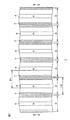
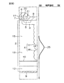
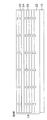
図1は、本発明の一実施形態に係る半導体装置1の模式的な平面図である。図2は、図1のII−II切断面における断面図である。なお、図1では、説明に必要な構成のみを示しており、たとえばn+型ソース領域5、ソース電極8等の図示を省略している。
半導体装置1は、スーパージャンクション構造を有するnチャンネル型MOSFET(Metal Oxide Semiconductor Field Effect Transistor)である。
Hereinafter, embodiments of the present invention will be described in detail with reference to the accompanying drawings.
FIG. 1 is a schematic plan view of a
The
半導体装置1は、n型半導体層2と、p型ボディ領域3と、本発明の第1ピラー層の一例としてのp型ピラー層4と、n+型ソース領域5と、ゲート絶縁膜6と、ゲート電極7と、ソース電極8と、ドレイン電極9と、トラップレベル領域10とを含む。ゲート電極7上には、層間絶縁膜11が配置されている。
n型半導体層2は、たとえば、本発明のドレイン領域の一例としてのn+型基板12と、当該n+型基板12上に半導体結晶を成長させることによって形成されたn−型エピタキシャル層13とを含んでいてもよい。
The
The n-
n+型基板12およびn−型エピタキシャル層13は、この実施形態ではシリコン(Si)からなる。n+型基板12に関して、その厚さは150μm〜180μm程度であってもよいし、そのn型不純物濃度は1×1018cm−3〜3×1018cm−3程度であってもよい。一方、n−型エピタキシャル層13に関して、その厚さは50μm〜90μm程度であってもよいし、そのn型不純物濃度は1×1015cm−3〜2×1015cm−3程度であってもよい。なお、n+型基板12およびn−型エピタキシャル層13に含有されるn型不純物としては、P(リン)、As(ヒ素)、SB(アンチモン)等を適用できる。
In this embodiment, the n + type substrate 12 and the n −
p型ボディ領域3およびp型ピラー層4は、p型不純物が注入された不純物領域である。より具体的には、n−型エピタキシャル層13に対してp型不純物をイオン注入(インプラ)することによって形成された不純物領域であってもよい。p型ボディ領域3およびp型ピラー層4に含有されるp型不純物としては、B(ホウ素)、Al(アルミニウム)、Ga(ガリウム)等を適用できる。
The p-
p型ボディ領域3は、図1に示すように、n−型エピタキシャル層13の表面の法線方向から見た平面視(以下、単に「平面視」とする)において周期的に離散配置された複数の領域において、n−型エピタキシャル層13の表面部に選択的に形成されている。この実施形態では、複数のp型ボディ領域3は、互いに平行なストライプ状に形成されている。個々のp型ボディ領域3およびその周囲のn−型エピタキシャル層13を含む領域は、セル14を形成している。すなわち、この半導体装置1は、図1のレイアウトでは、平面視においてストライプ状に配列された多数(複数)のセル14を有している。
As shown in FIG. 1, p-
p型ピラー層4は、平面視において、各セル14のp型ボディ領域3の内方の領域に形成されている。より具体的には、この実施形態では、p型ピラー層4は、平面視において、p型ボディ領域3の幅方向中央の領域においてストライプ状に形成されている。これにより、n−型エピタキシャル層13には、p型ピラー層4と共に、隣り合うp型ピラー層4で挟まれたn−型エピタキシャル層13の部分からなる本発明の第2ピラー層の一例としてのn−型ピラー層15が配置されている。
The p-
より具体的には、p型ピラー層4は、2μm〜6μmの幅、および3×1015cm−3〜8×1015cm−3の不純物濃度を有していてもよい。また、n−型ピラー層15は、2μm〜10μmの幅、および1×1015cm−3〜3×1015cm−3の不純物濃度を有していてもよい。
p型ピラー層4は、p型ボディ領域3に連なるように形成されており、n−型エピタキシャル層13において、p型ボディ領域3よりも深い位置までn+型基板12に向かって延びている。したがって、p型ピラー層4は、隣り合うp型ボディ領域3との間に連続性を持って配列されている。p型ピラー層4のピッチP1は、たとえば、5μm〜20μmである。ここで、ピッチP1とは、一対のp型ピラー層4およびn−型ピラー層15を一つの繰り返し単位とし、当該繰り返し単位のn−型エピタキシャル層13の表面に沿う方向の長さのことである。この実施形態では、p型ピラー層4が各p型ボディ領域3の幅方向中央に配置されていることから、ピッチP1はセル14のピッチ(セルピッチ)に一致している。
More specifically, the p-
The p-
p型ピラー層4は、その深さ方向途中部にn−型エピタキシャル層13の一部からなる分断領域16を介在させることによって上下に分断されていてもよい。p型ピラー層4は、分断領域16によって隔てられた上側ピラー層17および下側ピラー層18を含んでいてもよい。
各ピラー層17,18のn−型エピタキシャル層13の深さ方向に沿う側面は、当該方向に沿って周期的に起伏した凹凸面となっている。この凹凸の数は、通常、後述するn型半導体層23,24(図3A)の段数とほぼ一致するが、図2では明瞭化のために前記段数より少ない凹凸を表している。
The p-
Side surfaces of the pillar layers 17 and 18 along the depth direction of the n − -
上側ピラー層17は、p型ボディ領域3と一体をなしていて、p型ボディ領域3と共にn−型エピタキシャル層13との界面(pn接合面)に寄生ダイオード19を形成している。一方、下側ピラー層18は、p型ボディ領域3とは分断領域16によって分離されていて、電気的にフローティングされている。
n+型ソース領域5は、平面視において各セル14のp型ボディ領域3の内方領域に形成されている。n+型ソース領域5は、当該領域において、p型ボディ領域3の表面部に選択的に形成されている。n+型ソース領域5は、p型ボディ領域3にn型不純物を選択的にイオン注入することによって形成されてもよい。n型不純物の例は、前述のとおりである。n+型ソース領域5は、p型ボディ領域3の周縁(p型ボディ領域3とn−型エピタキシャル層13との界面)から所定距離だけ内側に位置するようにp型ボディ領域3内に形成されている。これにより、n−型エピタキシャル層13およびp型ボディ領域3等を含むn型半導体層2の表層領域において、n+型ソース領域5とn−型エピタキシャル層13との間には、p型ボディ領域3の表面部が介在し、この介在している表面部がチャネル領域20を提供する。
The
The n +
この実施形態では、n+型ソース領域5は、平面視ストライプ状に形成されており、p型ピラー層4の側面よりも外側の領域に形成されている。チャネル領域20は、n+型ソース領域5の形状に応じて、ストライプ状の形状を有している。
ゲート絶縁膜6は、たとえば、シリコン酸化膜、シリコン窒化膜、シリコン酸窒化膜、ハフニウム酸化膜、アルミナ膜、タンタル酸化膜等からなっていてもよい。ゲート絶縁膜6は、少なくともチャネル領域20におけるp型ボディ領域3の表面を覆うように形成されている。この実施形態では、ゲート絶縁膜6は、n+型ソース領域5の一部、チャネル領域20、およびn−型エピタキシャル層13の表面を覆うように形成されている。より端的には、ゲート絶縁膜6は、各セル14のp型ボディ領域3の中央領域およびこの領域に連なるn+型ソース領域5の内縁領域に開口を有するパターンで形成されている。
In this embodiment, the n + -
The
ゲート電極7は、ゲート絶縁膜6を介してチャネル領域20に対向するように形成されている。ゲート電極7は、たとえば、不純物を注入して低抵抗化したポリシリコンからなっていてもよい。この実施形態では、ゲート電極7は、ゲート絶縁膜6とほぼ同じパターンに形成されており、ゲート絶縁膜6の表面を覆っている。すなわち、ゲート電極7は、n+型ソース領域5の一部、チャネル領域20、およびn−型エピタキシャル層13の表面の上方に配置されている。より端的には、ゲート電極7は、各セル14のp型ボディ領域3の中央領域およびこの領域に連なるn+型ソース領域5の内縁領域に開口を有するパターンで形成されている。すなわち、ゲート電極7は、複数のセル14を共通に制御するように形成されている。これにより、プレーナゲート構造が構成されている。
The
層間絶縁膜11は、たとえば、シリコン酸化膜、シリコン窒化膜、TEOS(テトラエトキシシラン)等の絶縁材料からなる。層間絶縁膜11は、ゲート電極7を覆い、各セル14のp型ボディ領域3の中央領域およびこの領域に連なるn+型ソース領域5の内縁領域にコンタクト孔21を有するパターンで形成されている。
ソース電極8は、アルミニウムその他の金属からなる。ソース電極8は、層間絶縁膜11の表面を覆い、かつ各セル14のコンタクト孔21に埋め込まれるように形成されている。これにより、ソース電極8は、n+型ソース領域5にオーミック接続されている。したがって、ソース電極8は、複数のセル14に並列に接続されており、複数のセル14に流れる全電流が流れるように構成されている。また、ソース電極8は、コンタクト孔21を介して各セル14のp型ボディ領域3にオーミック接続されており、p型ボディ領域3の電位を安定化する。
The
The
ドレイン電極9は、アルミニウムその他の金属からなる。ドレイン電極9は、n+型基板12の裏面に接するように形成されている。これにより、ドレイン電極9は、複数のセル14に並列に接続されており、複数のセル14に流れる全電流が流れるように構成されている。
ドレイン電極9を高電位側、ソース電極8を低電位側として、ソース電極8およびドレイン電極9の間に直流電源を接続すると、寄生ダイオード19には逆バイアスが与えられる。このとき、ゲート電極7に所定の閾値電圧よりも低い制御電圧が与えられていると、ドレイン−ソース間には電流経路が形成されない。すなわち、半導体装置1は、オフ状態となる。一方、ゲート電極7に閾値電圧以上の制御電圧を与えると、チャネル領域20の表面に電子が引き寄せられて反転層(チャネル)が形成される。これにより、n+型ソース領域5とn−型エピタキシャル層13との間が導通する。すなわち、ソース電極8から、n+型ソース領域5、チャネル領域20の反転層、n−型エピタキシャル層13を順に通って、ドレイン電極9に至る電流経路が形成される。すなわち、半導体装置1は、オン状態となる。
The
When a direct current power source is connected between the
電動モータ等の誘導性負荷を駆動するインバータ回路に半導体装置1が適用されるとき、ソース電極8がドレイン電極9よりも高電位となって、寄生ダイオード19がオンし、この寄生ダイオード19を通って電流が流れる場合がある。その後、ソース電極8がドレイン電極9よりも低電位となると、寄生ダイオード19は、逆バイアス状態となって、ターンオフする。このターンオフ時には、寄生ダイオード19のpn接合部から空乏層が広がり、p型ボディ領域3およびp型ピラー層4内のキャリア(正孔)がソース電極8側に移動し、n−型エピタキシャル層13内のキャリア(電子)がドレイン電極9側へと移動する。
When the
このキャリアの移動によって、寄生ダイオード19がオン状態のときとは逆方向への電流が流れる。この電流は、逆回復電流とよばれる。逆回復電流は、一旦増加し、その後に減少する。ダイオードの順方向電流が零となってから、逆回復電流の大きさがその最大値の10%にまで減少するまでの時間は逆回復時間と呼ばれる。逆回復電流の変化(dir/dt)が大きいときは、電流が零に収束するまでに振動(リンギング)が生じる場合がある。このような逆回復特性は、ハードリカバリと呼ばれ、ノイズや誤動作の原因となる。
Due to this carrier movement, a current flows in a direction opposite to that when the
トラップレベル領域10は、逆回復時間の短縮に寄与する。トラップレベル領域10は、n型半導体層2の裏面側から荷電粒子を照射することによって形成された領域である。トラップレベル領域10には、キャリアをトラップして再結合させることによって消失させる再結合中心が多く存在している。これにより、寄生ダイオード19がターンオフするときにキャリアを速やかに消失させることができるから、逆回復時間および逆回復電流を低減できる。
The
トラップレベル領域10は、n−型エピタキシャル層13内において、n−型エピタキシャル層13の裏面から予め設定された深さ位置に薄く(たとえば1μm〜3μm程度の厚さで)広がるように局所的に形成されている。
トラップレベル領域10の形成には、プロトン、重水素、3He++、4He++等の荷電粒子の照射を適用することができる。なかでも、質量の大きなヘリウム原子核(3He++、または4He++)は、再結合中心の厚さ方向の分布域を狭くすることができ、厚さ方向に関して狭い範囲に再結合中心を局所的に分布させることができるので、好ましい。
For the formation of the
また、この半導体装置1では、p型ピラー層4が上下に分断されていて、下側ピラー層18はp型ボディ領域3に対して電気的にフローティングされている。したがって、寄生ダイオード19の動作に当該下側ピラー層18が寄与しないので、逆回復現象の際の急峻な空乏層の広がりが抑制される。これにより、ドレイン電極9に向かう空乏層の広がりが抑制され、それによって、寄生ダイオード19がターンオフするときに空乏層が広がる速さが抑制される。これにより、逆回復電流の変化速度(dir/dt)が小さくなるので、リカバリ特性が改善される。
In the
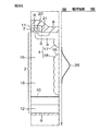
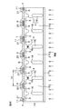
図3A〜図3Hは、それぞれ、n型半導体層2における電界集中部とトラップレベル領域10との位置関係を示す図である。
本願発明者は、n型半導体層2における電界集中部とトラップレベル領域10との位置関係について、条件をいくつかのパターンに動かしてシミュレーションを行い、どのような条件のときに電界集中部とトラップレベル領域10との位置が離れ、または近くなるのかを検証した。つまり、下記の条件等を入力してシミュレーションすることによって、半導体装置を実際に製造したときに電界集中部がどの位置になるか判定することができる。結果を図3A〜図3Hに示す。図3A〜図3Hでは、半導体装置1の構造(要部)の横側に、n型半導体層2の深さ方向における電界強度をグラフで示しており、符号25は電界強度が集中している電界集中部を示す。図3A〜図3Hの各図の条件は次の通りである。
3A to 3H are diagrams showing the positional relationship between the electric field concentration portion and the
The inventor of the present application performs a simulation on the positional relationship between the electric field concentration portion and the
図3A:ピラー分断なし
図3B:ピラー分断なし
図3C:ピラー分断なし
図3D:ピラー分断あり(下から3段目)
図3E:ピラー分断あり(下から7段目)
図3F:ピラー分断あり(下から3段目)
図3G:ピラー分断あり(下から7段目)
図3H:ピラー分断あり(下から7段目)
図3A〜図3Hの結果、条件を動かすことによって、図3C、図3D、図3E、図3Gおよび図3Hにおいて、n型半導体層2における電界集中部25とトラップレベル領域10とを互いに異なる深さ位置に配置することができた。たとえば、図3Dおよび図3Eでは、トラップレベル領域10がp型ピラー層4の底部の近傍に配置されている一方、電界集中部25は、それぞれ、p型ピラー層4の分断領域16の深さ位置に配置されている。また、図3Gおよび図3Hでは、電界集中部25が分断領域16の深さ位置ではないが、トラップレベル領域10よりも浅い位置に配置されていることで、電界集中部25とトラップレベル領域10とを離すことができている。
Fig. 3A: No pillar division Fig. 3B: No pillar division Fig. 3C: No pillar division Fig. 3D: Pillar division (third step from the bottom)
Fig. 3E: Pillar parting (7th step from the bottom)
Fig. 3F: Pillar parting (third step from the bottom)
Fig. 3G: Pillar parting (7th step from the bottom)
Fig. 3H: Pillar parting (7th step from the bottom)
As a result of FIGS. 3A to 3H, the electric
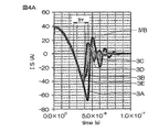
さらに、図3A〜図3Hのうち、図3A〜図3Eについては逆回復特性についても検証した。結果を図4A、図4B、図5Aおよび図5Bに示す。これらの図によれば、電界集中の緩和効果が見込まれた図3C、図3Dおよび図3Eのすべてにおいて、トラップレベル領域10が形成されていない図3Aの構造に比べて逆回復時間trr(図4Aでは、3Eのtrrのみ示している)を短縮でき、その他の逆回復特性も改善(逆回復電流の低減、逆回復電圧の低減、逆回復電流のリンギングの低減等)できていることがわかった。すなわち、少なくとも図3C、図3Dおよび図3Eの構成であれば、スーパージャンクション構造の半導体装置1の逆回復特性を改善できることが分かった。
Further, among FIGS. 3A to 3H, the reverse recovery characteristics were also verified for FIGS. 3A to 3E. The results are shown in FIGS. 4A, 4B, 5A and 5B. According to these figures, in all of FIGS. 3C, 3D, and 3E in which the effect of reducing the electric field concentration is expected, the reverse recovery time trr (FIG. 3) is compared with the structure of FIG. 3A where the
次に、半導体装置1の製造方法について説明する。
図6A〜図6Dは、半導体装置1の製造方法を工程順に示す図である。
半導体装置1を製造するには、たとえば図6Aに示すように、n+型基板12上に、n型の初期ベース層22が形成される。エピタキシャル成長の条件は、たとえば、1Ω・cm〜10Ω・cm、厚さ5μm〜20μmである。
Next, a method for manufacturing the
6A to 6D are diagrams showing a method of manufacturing the
To manufacture the
次に、図6Bに示すように、初期ベース層22の上に、p型ピラー層4を形成すべき位置にp型不純物を選択的に注入(Bイオンを50keV、5.3×1013cm−2、0度で注入)しながら1Ω・cm〜10Ω・cm/2μm〜10μmの薄いn型半導体層23を形成する工程を繰り返すマルチエピタキシャル成長によって、複数層のn型半導体層23を積層させる。その後、n型半導体層23と同じ抵抗および厚さ(1Ω・cm〜10Ω・cm/2μm〜10μm)のn型半導体層24を、p型不純物を注入しないで一段成長させる。次に、再びn型半導体層23をマルチエピタキシャル成長させる。これにより、複数枚のn型半導体層23,24と初期ベース層22とが一体化されてn−型エピタキシャル層13が形成される。
Next, as shown in FIG. 6B, a p-type impurity is selectively implanted on the
次に、図3Cに示すように、アニール処理(1000℃〜1200℃)を行うことによって、複数層のn型半導体層23,24のp型不純物をドライブ拡散させる。これにより、途中で分断されたp型ピラー層4が形成される。すなわち、n型半導体層24よりも下側のn型半導体層23内のp型不純物が拡散によって下側ピラー層18を提供し、n型半導体層24よりも上側のn型半導体層23内のp型不純物が拡散によって上側ピラー層17を提供し、これらの間のn型半導体層24の位置に分断領域16を提供する。
Next, as shown in FIG. 3C, an annealing process (1000 ° C. to 1200 ° C.) is performed to drive diffuse the p-type impurities in the plurality of n-type semiconductor layers 23 and 24. Thereby, the p-
次に、n−型エピタキシャル層13の表面部に選択的に比較的低いエネルギでp型不純物が注入(Bイオンを50keV、5.0×1015cm−2、7度で注入)されて、p型ボディ領域3が形成される。また、平面視においてp型ボディ領域3内においてp型ボディ領域3の外周縁から所定距離だけ内方に後退した位置に外縁部を有する所定幅の環状領域にn型不純物が選択的に注入(Pイオンを130keV、2.0×1015cm−2、7度で注入)され、これにより、n+型ソース領域5が形成される。
Next, a p-type impurity is selectively implanted into the surface portion of the n − -
次に、n−型エピタキシャル層13およびp型ボディ領域3の表面(半導体結晶の表面)を覆うように、ゲート絶縁膜6が形成される。このゲート絶縁膜6は、半導体結晶表面の熱酸化によって形成されてもよい。さらに、ゲート絶縁膜6上に、ゲート電極7が形成される。ゲート電極7の形成は、たとえば、不純物を添加して低抵抗化したポリシリコン膜を全表面に形成し、その後、そのポリシリコン膜をフォトリソグラフィによって選択的にエッチングすることによって行ってもよい。このエッチングのときには、ゲート絶縁膜6を同時にパターニングして、ゲート電極7およびゲート絶縁膜6を同一パターンに形成してもよい。さらに、ゲート電極7を覆うように、層間絶縁膜11(たとえば、10000Å厚)が形成され、この層間絶縁膜11に、フォトリソグラフィによって、コンタクト孔21が形成される。次に、層間絶縁膜11上に、ソース電極8が形成され、必要に応じて、合金化によるオーミック接合形成のための熱処理が行われる。この後、図示しない表面保護膜(たとえば、16000Å厚)が形成され、その表面保護膜に、ソース電極8の一部をパッドとして露出させるパッド開口が形成される。
Next,
次に、図6Dに示すように、n型半導体層2の裏面から、荷電粒子照射が行われる。このときに照射される荷電粒子としては、たとえばプロトン、重水素、3He++、4He++が用いられる。その後、低温の熱処理(低温アニール)が行われる。これにより、照射された荷電粒子が活性化する。荷電粒子としてヘリウム原子核(3He++または4He++)を選択した場合には、たとえば、320℃〜380℃(たとえば350℃)で30分〜120分程度(たとえば60分)の熱処理によって活性化できる。
Next, as shown in FIG. 6D, charged particle irradiation is performed from the back surface of the n-
こうして、トラップレベル領域10が形成される。荷電粒子を照射するときのエネルギを大きくすれば荷電粒子の飛程が長くなるから、n型半導体層2の裏面から遠い位置にトラップレベル領域10が形成され、そのエネルギを小さくすれば荷電粒子の飛程が短くなるから、n型半導体層2の裏面から近い位置にトラップレベル領域10が形成される。したがって、トラップレベル領域10の配置に応じて、荷電粒子の照射エネルギが設定される。
Thus, the
この後、n+型基板12の裏面にドレイン電極9が形成され、必要に応じて、合金化によるオーミック接合形成のための熱処理が行われる。
以上の工程を経て、図1および図2の半導体装置1を得ることができる。
図7は、本発明の他の実施形態に係る半導体装置31の模式的な平面図である。図8は、図7のVIII−VIII切断面における断面図である。図7および図8において、前述の図1および図2に示された各部と対応する部分には同一の参照符号を付して示し、その説明を省略する。
Thereafter, the
Through the above steps, the
FIG. 7 is a schematic plan view of a
半導体装置31は、n+型基板12が省略されている点が、前述の半導体装置1と異なっている。より具体的には、半導体装置31は、ドレイン電極9のコンタクトをとるための層として、n+型基板12に代えて、本発明のドレイン領域の一例としてのn+型コンタクト領域32を有している。
n+型コンタクト領域32は、n−型エピタキシャル層13の裏面全体にわたって形成されている。n+型コンタクト領域32は、p型ピラー層4の底部に対して間隔が空くような深さで形成されている。これにより、p型ピラー層4とn+型コンタクト領域32との間には、n−型エピタキシャル層13が介在している。
The
The n +
また、半導体装置31は、n+型コンタクト領域32の裏面部に選択的にp+型コレクタ領域33を有している点において、前述の半導体装置1と異なっている。
p+型コレクタ領域33は、n−型エピタキシャル層13の裏面に選択的に形成され、当該裏面に沿って連続性を持って複数配列されている。この実施形態では、p+型コレクタ領域33は、図7にクロスハッチングで明示するように平面視においてp型ピラー層4に平行なストライプ状に形成されている。これにより、n−型エピタキシャル層13の裏面には、p+型コレクタ領域33と、隣り合うp+型コレクタ領域33間のn+型コンタクト領域32とがストライプ状に交互に露出することとなる。
The
The p +
p+型コレクタ領域33のピッチP2は、p型ピラー層4のピッチP1よりも大きくてもよい。これにより、半導体装置1は、n−型エピタキシャル層13の厚さ方向において、p+型コレクタ領域33に対向するp型ピラー層4と、p+型コレクタ領域33に対向せずに、隣り合うp+型コレクタ領域33の間のn型部分に対向するp型ピラー層4とを選択的に有することとなる。
The pitch P 2 of the p + -
さらにp+型コレクタ領域33の構成について説明を加えると、p+型コレクタ領域33の不純物濃度は、1×1017cm−3〜1×1022cm−3である。また、p+型コレクタ領域33は、n−型エピタキシャル層13の裏面からn+型コンタクト領域32を厚さ方向に貫通してn−型エピタキシャル層13に達するように形成されており、n−型エピタキシャル層13の裏面から0.2μm〜3μmの深さを有している。また、p+型コレクタ領域33の幅は、5μm〜200μmである。
Further addition of explanation of the structure of the p + -
そして、この半導体装置31によれば、n−型エピタキシャル層13の裏面に複数のp+型コレクタ領域33が選択的に形成されているので、当該裏面にはn−型エピタキシャル層13とp+型コレクタ領域33の両方が露出することとなる。これにより、n−型エピタキシャル層13の裏面に、当該露出したn−型エピタキシャル層13およびp+型コレクタ領域33の両方に接するようにドレイン電極9を形成することによって、低電流域でのセット効率に優れるMOSFETの特性と、高電圧域において伝導度変調を発生させることができるIGBTの特性とを併せ持つ半導体装置31を提供することができる。むろん、前述の半導体装置1と同様の作用効果を実現することもできる。
Then, according to the
図9A〜図9Hは、半導体装置31の製造工程の一部を工程順に示す図である。図9A〜図9Hにおいて、前述の図6A〜図6Dに示された各部と対応する部分には同一の参照符号を付して示し、その説明を省略する。
半導体装置31を製造するには、たとえば図9Aに示すように、基板34上に、n型不純物を注入しながら行うエピタキシャル成長によって、初期ベース層22が形成される。基板34としては、n型シリコン基板を採用することができるが、この基板34は後の工程で除去するものであるので、高品質なものである必要はなく、安価な基板を使用することができる。
9A to 9H are diagrams illustrating a part of the manufacturing process of the
To manufacture the
次に、図9Bに示すように、初期ベース層22の上に、複数層のn型半導体層23、単層のn型半導体層24および複数のn型半導体層23を順にエピタキシャル成長させる。
次に、図9Cに示すように、アニール処理(1000℃〜1200℃)を行うことによって、複数層のn型半導体層23,24のp型不純物をドライブ拡散させる。これにより、途中で分断されたp型ピラー層4が形成される。次に、前述と同様の方法によって、p型ボディ領域3、n+型ソース領域5、ゲート絶縁膜6、ゲート電極7、層間絶縁膜11およびソース電極8が形成される。
Next, as shown in FIG. 9B, a plurality of n-type semiconductor layers 23, a single n-
Next, as shown in FIG. 9C, an annealing process (1000 ° C. to 1200 ° C.) is performed to drive diffuse the p-type impurities in the multiple layers of the n-type semiconductor layers 23 and 24. Thereby, the p-
次に、図9Dに示すように、たとえばグラインダを用いて基板34を裏面側から研削する。この研削は、たとえば、基板34を完全に除去してn−型エピタキシャル層13の裏面が露出した後、p型ピラー層4の直下のn−型エピタキシャル層13が一定の厚さで残るように行ってもよい。研削後、n−型エピタキシャル層13の裏面をスピンエッチングすることによって裏面を鏡面に仕上げる。
Next, as shown in FIG. 9D, the
このように、製造工程の途中までn−型エピタキシャル層13が基板34に支持されているので、n−型エピタキシャル層13の搬送・ハンドリングを行い易くすることができる。また、基板34の研削に続けてn−型エピタキシャル層13の研削を連続して実行することができるので、p型ピラー層4の直下のn−型エピタキシャル層13の厚さを簡単に調節することができる。
Thus, since the n −
次に、図9Eに示すように、n−型エピタキシャル層13の裏面から、荷電粒子照射が行われる。その後、低温の熱処理(低温アニール)が行われる。これにより、照射された荷電粒子が活性化する。こうして、トラップレベル領域10が形成される。
次に、図9Fに示すように、n−型エピタキシャル層13の裏面へ向かってn型不純物を全面に注入(Asイオンを30keV、1.0×1015cm−2、0度で注入)し、アニール処理することによって、n+型コンタクト領域32が形成される。
Next, as shown in FIG. 9E, charged particle irradiation is performed from the back surface of the n − -
Next, as shown in FIG. 9F, an n-type impurity is implanted into the entire surface toward the back surface of the n − -type epitaxial layer 13 (As ions are implanted at 30 keV, 1.0 × 10 15 cm −2 , 0 degree). By performing the annealing process, the n + -
次に、図9Gに示すように、n−型エピタキシャル層13の裏面を選択的に露出させるフォトレジスト35が形成される。そして、このフォトレジスト35を介して、まずBイオンを100keV、1.0×1015cm−2、7度の傾斜角度で注入する。続けて、Bイオンを注入する工程よりも小さなエネルギ、具体的には、30keV、1.0×1015cm−2、7度(同じ傾斜角度)でBF2イオンを注入する。この際、BイオンおよびBF2イオンをn−型エピタキシャル層13の裏面に対して垂直ではなく、所定の傾斜角度を持たせて斜め注入することによって、イオンがn−型エピタキシャル層13の深くまで入っていくチャネリングを防止することができる。この後、フォトレジスト35を、たとえばアッシングによって除去する。
Next, as shown in FIG. 9G, a
次に、図9Hに示すように、n−型エピタキシャル層13をレーザアニール処理することによって、前工程で注入したBイオンおよびBF2イオンを活性化させる。これにより、n+型コンタクト領域32の一部の導電型がn型からp型へと反転して、p+型コレクタ領域33が形成される。
このとき、高温(たとえば1500℃程度)のアニール処理を実行しないので、ソース電極8の溶融を防止することができる。つまり、ソース電極8などの高温環境下で溶融し易い金属系の部分を、このアニール処理に先立って作製することができる。そのため、n−型エピタキシャル層13の表面側の構造の大部分もしくは全てを、当該アニール処理を行う前に作製することができる。その結果、n−型エピタキシャル層13の表裏面を何度も逆にしなくて済むので、製造効率を向上させることができる。
Next, as shown in FIG. 9H, the n −
At this time, since annealing at a high temperature (for example, about 1500 ° C.) is not performed, melting of the
この後、n−型エピタキシャル層13の裏面にドレイン電極9が形成され、必要に応じて、合金化によるオーミック接合形成のための熱処理が行われる。
以上の工程を経て、図7および図8の半導体装置31を得ることができる。
以上、本発明の実施形態について説明したが、本発明は、さらに他の形態で実施することもできる。
Thereafter, the
Through the above steps, the
As mentioned above, although embodiment of this invention was described, this invention can also be implemented with another form.
たとえば、図10に示す半導体装置41のように、トレンチゲート構造を有していてもよい。具体的には、n型半導体層2の表面からn+型ソース領域5およびp型ボディ領域3を貫通するゲートトレンチ42が形成され、当該ゲートトレンチ42に、ゲート絶縁膜43を介してゲート電極44が充填されたトレンチゲート構造を有していてもよい。
また、半導体装置1,31,41の各半導体部分の導電型を反転した構成が採用されてもよい。たとえば、半導体装置1において、p型の部分がn型であり、n型の部分がp型であってもよい。
For example, a
Moreover, the structure which reversed the conductivity type of each semiconductor part of the
その他、特許請求の範囲に記載された事項の範囲で種々の設計変更を施すことが可能である。 In addition, various design changes can be made within the scope of matters described in the claims.
1 半導体装置
2 n型半導体層
3 p型ボディ領域
4 p型ピラー層
5 n+型ソース領域
6 ゲート絶縁膜
7 ゲート電極
10 トラップレベル領域
12 n+型基板
13 n−型エピタキシャル層
15 n−型ピラー層
16 分断領域
25 電界集中部
31 半導体装置
32 n+型コンタクト領域
33 p+型コレクタ領域
41 半導体装置
42 ゲートトレンチ
43 ゲート絶縁膜
44 ゲート電極
1 semiconductor device 2 n-type semiconductor layer 3 p-type body region 4 p-type pillar layer 5 n + -
Claims (11)
前記半導体層の表面部に配置された第2導電型のボディ領域と、
前記ボディ領域の表面部に配置された第1導電型のソース領域と、
前記ボディ領域に対向するゲート電極と、
前記ボディ領域と前記ゲート電極との間のゲート絶縁膜と、
前記ボディ領域に連なるように前記半導体層内に配置され、前記ボディ領域から前記半導体層の前記裏面に向かって延びた第2導電型の第1ピラー層と、
前記半導体層内に配置され、トラップレベルを形成する荷電粒子を含むトラップレベル領域とを含み、
前記第1ピラー層の深さ方向において、前記ボディ領域にチャネルが形成されていないオフ状態のときに電界が集中する電界集中部と、前記トラップレベル領域とが互いに異なる深さ位置に配置されている、半導体装置。 A semiconductor layer having a drain region of the first conductivity type on the back side;
A body region of a second conductivity type disposed on the surface portion of the semiconductor layer;
A source region of a first conductivity type disposed on a surface portion of the body region;
A gate electrode facing the body region;
A gate insulating film between the body region and the gate electrode;
A first pillar layer of a second conductivity type disposed in the semiconductor layer so as to be continuous with the body region and extending from the body region toward the back surface of the semiconductor layer;
A trap level region disposed within the semiconductor layer and including charged particles forming a trap level;
In the depth direction of the first pillar layer, the electric field concentration part where the electric field concentrates when the channel is not formed in the body region and the trap level region are arranged at different depth positions. A semiconductor device.
前記電界集中部は、前記分断領域に配置されている、請求項1〜3のいずれか一項に記載の半導体装置。 The first pillar layer is divided vertically by interposing a dividing region consisting of a part of the semiconductor layer in the middle in the depth direction,
The semiconductor device according to claim 1, wherein the electric field concentration portion is disposed in the divided region.
前記半導体層には、前記複数の第1ピラー層の間に第1導電型の第2ピラー層が配置されており、
前記第1ピラー層と前記第2ピラー層とのチャージバランスが確保されている、請求項4に記載の半導体装置。 The first pillar layer includes a plurality of the first pillar layers arranged along the surface of the semiconductor layer,
In the semiconductor layer, a second pillar layer of a first conductivity type is disposed between the plurality of first pillar layers,
The semiconductor device according to claim 4, wherein a charge balance between the first pillar layer and the second pillar layer is ensured.
前記第2ピラー層は、2μm〜10μmの幅、および1×1015cm−3〜3×1015cm−3の不純物濃度を有している、請求項5に記載の半導体装置。 The first pillar layer has a width of 2 μm to 6 μm and an impurity concentration of 3 × 10 15 cm −3 to 8 × 10 15 cm −3 ,
The semiconductor device according to claim 5, wherein the second pillar layer has a width of 2 μm to 10 μm and an impurity concentration of 1 × 10 15 cm −3 to 3 × 10 15 cm −3 .
Priority Applications (2)
| Application Number | Priority Date | Filing Date | Title |
|---|---|---|---|
| JP2016066392A JP2017183419A (en) | 2016-03-29 | 2016-03-29 | Semiconductor device |
| US15/461,018 US10103228B2 (en) | 2016-03-29 | 2017-03-16 | Semiconductor device having a super junction structure |
Applications Claiming Priority (1)
| Application Number | Priority Date | Filing Date | Title |
|---|---|---|---|
| JP2016066392A JP2017183419A (en) | 2016-03-29 | 2016-03-29 | Semiconductor device |
Publications (1)
| Publication Number | Publication Date |
|---|---|
| JP2017183419A true JP2017183419A (en) | 2017-10-05 |
Family
ID=59959801
Family Applications (1)
| Application Number | Title | Priority Date | Filing Date |
|---|---|---|---|
| JP2016066392A Pending JP2017183419A (en) | 2016-03-29 | 2016-03-29 | Semiconductor device |
Country Status (2)
| Country | Link |
|---|---|
| US (1) | US10103228B2 (en) |
| JP (1) | JP2017183419A (en) |
Cited By (7)
| Publication number | Priority date | Publication date | Assignee | Title |
|---|---|---|---|---|
| CN109449202A (en) * | 2018-10-30 | 2019-03-08 | 广州工商学院 | One kind is inverse to lead bipolar junction transistor |
| WO2019087341A1 (en) * | 2017-11-01 | 2019-05-09 | 新電元工業株式会社 | Semiconductor device and method for manufacturing semiconductor device |
| JP2019176077A (en) * | 2018-03-29 | 2019-10-10 | ローム株式会社 | Semiconductor device |
| WO2019224913A1 (en) * | 2018-05-22 | 2019-11-28 | サンケン電気株式会社 | Semiconductor device |
| JP2020047623A (en) * | 2018-09-14 | 2020-03-26 | 株式会社東芝 | Semiconductor device |
| WO2021200324A1 (en) * | 2020-03-31 | 2021-10-07 | ローム株式会社 | Semiconductor device |
| CN115172466A (en) * | 2022-09-05 | 2022-10-11 | 深圳市威兆半导体股份有限公司 | Novel super-junction VDMOS structure and preparation method thereof |
Families Citing this family (7)
| Publication number | Priority date | Publication date | Assignee | Title |
|---|---|---|---|---|
| IT201800006323A1 (en) | 2018-06-14 | 2019-12-14 | SEMICONDUCTOR DEVICE OF THE CHARGE BALANCING TYPE, IN PARTICULAR FOR HIGH EFFICIENCY RF APPLICATIONS, AND RELATED MANUFACTURING PROCESS | |
| CN109300978A (en) * | 2018-10-25 | 2019-02-01 | 上海超致半导体科技有限公司 | A kind of superjunction IGBT device structure and its manufacturing method |
| CN113808945A (en) * | 2020-06-12 | 2021-12-17 | 芯恩(青岛)集成电路有限公司 | Super junction power device and preparation method thereof |
| CN113517333A (en) * | 2021-06-07 | 2021-10-19 | 西安电子科技大学 | MOSFET device with super junction structure and preparation method thereof |
| CN116031303B (en) * | 2023-02-09 | 2023-11-21 | 上海功成半导体科技有限公司 | Super junction device, manufacturing method thereof and electronic device |
| CN117525151A (en) * | 2023-12-29 | 2024-02-06 | 深圳天狼芯半导体有限公司 | sJ MOS for improving reverse recovery characteristic and its preparation method |
| CN117525156A (en) * | 2024-01-05 | 2024-02-06 | 深圳天狼芯半导体有限公司 | MOSFET with anode Schottky contact and preparation method |
Citations (8)
| Publication number | Priority date | Publication date | Assignee | Title |
|---|---|---|---|---|
| JP2005191268A (en) * | 2003-12-25 | 2005-07-14 | Nec Electronics Corp | Semiconductor device and method of manufacturing same |
| JP2006261562A (en) * | 2005-03-18 | 2006-09-28 | Toyota Industries Corp | Semiconductor device |
| JP2008091450A (en) * | 2006-09-29 | 2008-04-17 | Toshiba Corp | Semiconductor element |
| WO2010024433A1 (en) * | 2008-09-01 | 2010-03-04 | ローム株式会社 | Semiconductor device and manufacturing method thereof |
| JP2012142330A (en) * | 2010-12-28 | 2012-07-26 | Rohm Co Ltd | Semiconductor device and manufacturing method of the same |
| JP2014209507A (en) * | 2013-04-16 | 2014-11-06 | ローム株式会社 | Semiconductor device |
| JP2014222710A (en) * | 2013-05-13 | 2014-11-27 | ローム株式会社 | Semiconductor device and manufacturing method of the same |
| JP2015018913A (en) * | 2013-07-10 | 2015-01-29 | 富士電機株式会社 | Super-junction mosfet, manufacturing method therefor, and composite semiconductor device with parallel connected diodes |
Family Cites Families (3)
| Publication number | Priority date | Publication date | Assignee | Title |
|---|---|---|---|---|
| JP4696986B2 (en) | 2006-03-17 | 2011-06-08 | トヨタ自動車株式会社 | Manufacturing method of semiconductor device having super junction structure |
| US9041096B2 (en) * | 2013-04-16 | 2015-05-26 | Rohm Co., Ltd. | Superjunction semiconductor device and manufacturing method therefor |
| JP2015070185A (en) | 2013-09-30 | 2015-04-13 | サンケン電気株式会社 | Semiconductor device and method of manufacturing the same |
-
2016
- 2016-03-29 JP JP2016066392A patent/JP2017183419A/en active Pending
-
2017
- 2017-03-16 US US15/461,018 patent/US10103228B2/en active Active
Patent Citations (8)
| Publication number | Priority date | Publication date | Assignee | Title |
|---|---|---|---|---|
| JP2005191268A (en) * | 2003-12-25 | 2005-07-14 | Nec Electronics Corp | Semiconductor device and method of manufacturing same |
| JP2006261562A (en) * | 2005-03-18 | 2006-09-28 | Toyota Industries Corp | Semiconductor device |
| JP2008091450A (en) * | 2006-09-29 | 2008-04-17 | Toshiba Corp | Semiconductor element |
| WO2010024433A1 (en) * | 2008-09-01 | 2010-03-04 | ローム株式会社 | Semiconductor device and manufacturing method thereof |
| JP2012142330A (en) * | 2010-12-28 | 2012-07-26 | Rohm Co Ltd | Semiconductor device and manufacturing method of the same |
| JP2014209507A (en) * | 2013-04-16 | 2014-11-06 | ローム株式会社 | Semiconductor device |
| JP2014222710A (en) * | 2013-05-13 | 2014-11-27 | ローム株式会社 | Semiconductor device and manufacturing method of the same |
| JP2015018913A (en) * | 2013-07-10 | 2015-01-29 | 富士電機株式会社 | Super-junction mosfet, manufacturing method therefor, and composite semiconductor device with parallel connected diodes |
Cited By (15)
| Publication number | Priority date | Publication date | Assignee | Title |
|---|---|---|---|---|
| WO2019087341A1 (en) * | 2017-11-01 | 2019-05-09 | 新電元工業株式会社 | Semiconductor device and method for manufacturing semiconductor device |
| WO2019087424A1 (en) * | 2017-11-01 | 2019-05-09 | 新電元工業株式会社 | Semiconductor device and method for manufacturing semiconductor device |
| JPWO2019087424A1 (en) * | 2017-11-01 | 2020-01-16 | 新電元工業株式会社 | Semiconductor device and method of manufacturing semiconductor device |
| US10818496B2 (en) | 2017-11-01 | 2020-10-27 | Shindengen Electric Manufacturing Co., Ltd. | Semiconductor device having crystal defects and method of manufacturing the semiconductor device having crystal defects |
| JP2019176077A (en) * | 2018-03-29 | 2019-10-10 | ローム株式会社 | Semiconductor device |
| JP7007971B2 (en) | 2018-03-29 | 2022-01-25 | ローム株式会社 | Semiconductor device |
| JPWO2019224913A1 (en) * | 2018-05-22 | 2021-05-27 | サンケン電気株式会社 | Semiconductor device |
| WO2019224913A1 (en) * | 2018-05-22 | 2019-11-28 | サンケン電気株式会社 | Semiconductor device |
| JP2020047623A (en) * | 2018-09-14 | 2020-03-26 | 株式会社東芝 | Semiconductor device |
| JP7055725B2 (en) | 2018-09-14 | 2022-04-18 | 株式会社東芝 | Semiconductor device |
| CN109449202B (en) * | 2018-10-30 | 2021-10-22 | 广州工商学院 | Reverse conducting bipolar transistor |
| CN109449202A (en) * | 2018-10-30 | 2019-03-08 | 广州工商学院 | One kind is inverse to lead bipolar junction transistor |
| WO2021200324A1 (en) * | 2020-03-31 | 2021-10-07 | ローム株式会社 | Semiconductor device |
| CN115172466A (en) * | 2022-09-05 | 2022-10-11 | 深圳市威兆半导体股份有限公司 | Novel super-junction VDMOS structure and preparation method thereof |
| CN115172466B (en) * | 2022-09-05 | 2022-11-08 | 深圳市威兆半导体股份有限公司 | Novel super-junction VDMOS structure and preparation method thereof |
Also Published As
| Publication number | Publication date |
|---|---|
| US10103228B2 (en) | 2018-10-16 |
| US20170288021A1 (en) | 2017-10-05 |
Similar Documents
| Publication | Publication Date | Title |
|---|---|---|
| US10103228B2 (en) | Semiconductor device having a super junction structure | |
| JP6369173B2 (en) | Vertical semiconductor device and manufacturing method thereof | |
| JP6415749B2 (en) | Silicon carbide semiconductor device | |
| JP6037495B2 (en) | Semiconductor device and manufacturing method thereof | |
| JP6611532B2 (en) | Semiconductor device and manufacturing method of semiconductor device | |
| WO2016204098A1 (en) | Semiconductor device | |
| JP2014165306A (en) | Method of manufacturing superjunction semiconductor device | |
| JP7243744B2 (en) | Semiconductor device and method for manufacturing semiconductor device | |
| WO2018016208A1 (en) | Semiconductor device, and manufacturing method for same | |
| JP2017195224A (en) | Switching element | |
| US11251299B2 (en) | Silicon carbide semiconductor device and manufacturing method of same | |
| JP4910894B2 (en) | Semiconductor device manufacturing method and semiconductor device | |
| JPWO2020075248A1 (en) | Semiconductor devices and their manufacturing methods | |
| JP6234696B2 (en) | Semiconductor device | |
| JP6168513B2 (en) | Semiconductor device and manufacturing method thereof | |
| CN115241268A (en) | Semiconductor device with a plurality of semiconductor chips | |
| JP6780335B2 (en) | Manufacturing method of reverse blocking MOS type semiconductor device and reverse blocking MOS type semiconductor device | |
| JP3888997B2 (en) | Semiconductor device | |
| JP2005136092A (en) | Semiconductor device and its manufacturing method | |
| US11127850B2 (en) | Semiconductor device | |
| JP2014056881A (en) | Semiconductor device and semiconductor device manufacturing method | |
| JP6599957B2 (en) | Semiconductor device | |
| JP2019125625A (en) | Semiconductor device, and method of manufacturing semiconductor device | |
| US20230299131A1 (en) | Superjunction semiconductor device | |
| US20160049484A1 (en) | Semiconductor device |
Legal Events
| Date | Code | Title | Description |
|---|---|---|---|
| A621 | Written request for application examination |
Free format text: JAPANESE INTERMEDIATE CODE: A621 Effective date: 20190220 |
|
| A977 | Report on retrieval |
Free format text: JAPANESE INTERMEDIATE CODE: A971007 Effective date: 20191106 |
|
| A131 | Notification of reasons for refusal |
Free format text: JAPANESE INTERMEDIATE CODE: A131 Effective date: 20191212 |
|
| A521 | Request for written amendment filed |
Free format text: JAPANESE INTERMEDIATE CODE: A523 Effective date: 20200204 |
|
| A02 | Decision of refusal |
Free format text: JAPANESE INTERMEDIATE CODE: A02 Effective date: 20200528 |
|
| A521 | Request for written amendment filed |
Free format text: JAPANESE INTERMEDIATE CODE: A523 Effective date: 20200824 |
|
| C60 | Trial request (containing other claim documents, opposition documents) |
Free format text: JAPANESE INTERMEDIATE CODE: C60 Effective date: 20200824 |
|
| A911 | Transfer to examiner for re-examination before appeal (zenchi) |
Free format text: JAPANESE INTERMEDIATE CODE: A911 Effective date: 20200901 |
|
| C21 | Notice of transfer of a case for reconsideration by examiners before appeal proceedings |
Free format text: JAPANESE INTERMEDIATE CODE: C21 Effective date: 20200903 |
|
| A912 | Re-examination (zenchi) completed and case transferred to appeal board |
Free format text: JAPANESE INTERMEDIATE CODE: A912 Effective date: 20201016 |
|
| C211 | Notice of termination of reconsideration by examiners before appeal proceedings |
Free format text: JAPANESE INTERMEDIATE CODE: C211 Effective date: 20201022 |
|
| C22 | Notice of designation (change) of administrative judge |
Free format text: JAPANESE INTERMEDIATE CODE: C22 Effective date: 20210105 |
|
| C23 | Notice of termination of proceedings |
Free format text: JAPANESE INTERMEDIATE CODE: C23 Effective date: 20210624 |
|
| C03 | Trial/appeal decision taken |
Free format text: JAPANESE INTERMEDIATE CODE: C03 Effective date: 20210729 |
|
| C30A | Notification sent |
Free format text: JAPANESE INTERMEDIATE CODE: C3012 Effective date: 20210729 |