EP2325818A1 - Stromversorgungsfreie Ereignisdetektionsvorrichtung - Google Patents
Stromversorgungsfreie Ereignisdetektionsvorrichtung Download PDFInfo
- Publication number
- EP2325818A1 EP2325818A1 EP10191110A EP10191110A EP2325818A1 EP 2325818 A1 EP2325818 A1 EP 2325818A1 EP 10191110 A EP10191110 A EP 10191110A EP 10191110 A EP10191110 A EP 10191110A EP 2325818 A1 EP2325818 A1 EP 2325818A1
- Authority
- EP
- European Patent Office
- Prior art keywords
- input
- fet transistor
- detection device
- self
- reset
- Prior art date
- Legal status (The legal status is an assumption and is not a legal conclusion. Google has not performed a legal analysis and makes no representation as to the accuracy of the status listed.)
- Granted
Links
Images




Classifications
-
- E—FIXED CONSTRUCTIONS
- E05—LOCKS; KEYS; WINDOW OR DOOR FITTINGS; SAFES
- E05B—LOCKS; ACCESSORIES THEREFOR; HANDCUFFS
- E05B39/00—Locks giving indication of authorised or unauthorised unlocking
Definitions
- the present invention concerns a self-powered event detection device which comprises a sensor, activated by a physical or chemical action or phenomenon applied on it with at least a given strength or intensity, and a non-volatile memory for storing information relative to the detection of at least one physical or chemical action or phenomenon detected by said sensor.
- the present invention concerns a tamper event detection device for detecting a penetration in a protected zone or in a closed case or container.
- 'self-powered event detection device it is understood that there is no need for an internal or external power source supplying the device for allowing its sensor to be activated and to detect a specific physical or chemical action or phenomenon.
- a self-powered event detection device can be supplied with power for other functions in defined time periods, e.g. for reading the state of a memory or for resetting such a memory.
- the physical or chemical action or phenomenon to which the sensor is sensitive is also named an external event.
- 'external event' it is thus understood an action or a phenomenon that the sensor can detect, i.e. an action or a phenomenon applied on the sensing element of this sensor, and not an electrical signal from an external power source supplying the electronic circuit of such a sensor or a further electronic circuit associated to the sensor.
- the invention further specifically deals with the reduction of the power consumption of such self-powered detection devices and furthermore with the increase in their security level.
- the invention concerns such self-powered detection devices comprising a read circuit or being arranged to be coupled to such a read circuit for reading the state of the NVM and, in a particular case wherein the self-powered detection device can be reset, further comprising a reset circuit or being arranged to be coupled to such a reset circuit.
- Another method for the detection of an external event consists of the integration of electrical detection means internal to the electronic circuit, powering this electronic circuit and waiting for the event to occur while powered.
- the detection means can be a sensor that is configured to provide a detection signal when the sensor and the electronic circuit are powered, the occurrence of this signal being stored in a memory via a write control circuit which is also powered by a power source.
- the supply of power for the event detection device needs to be a battery or another power source supplying continuous power. Without such a power source or if the power source is OFF or if the energy stored in the battery becomes too low, this device will not be functional, i.e., it will be incapable of detecting and recording an event.
- the patent application EP 0 592 097 proposes a penetration detection system which overcomes the above mentioned problem concerning the power supply.
- This detection system comprises a sensing piezoelectric transducer and a memorizing piezoelectric transducer.
- the positive pole and the negative pole of the sensing piezoelectric transducer are respectively connected to the negative and positive poles of the memorizing piezoelectric transducer.
- the memorizing transducer comprises a layer of piezoelectric material having a thickness selected such that, upon mechanical probing of the sensing transducer, an electrical signal produced by this sensing transducer will be sufficient to effect a reversal in the poling of the memorizing transducer.
- This system defines a self-powered detection device.
- this detection device is expensive and not well adapted to be integrated in a small volume device because it comprises two distinct piezoelectric transducers. As shown in this patent application, these two transducers form two separate discrete units which are electrically connected and the memorizing transducer is linked to other classical electronic elements which are not manufactured with a same technology as this memorizing transducer. Thus, an integration of the memorizing piezoelectric transducer with further electronic elements, e.g. a reading circuit, will not be possible with a classical microelectronic process. Further, the reading means are complex and not adapted to integrated circuits.
- the patent application US 2002/0190610 describes a self-powered remote control device comprising transmitting means, a feeder circuit connected to said transmitting means, a generator supplying electric power connected to the feeder circuit, and control means associated with the electric power generator.
- the generator comprises at least a piezoelectric element receiving mechanical stresses produced by actuating the control means and supplying electrical power to the feeder circuit.
- the feeder circuit comprises a rectifier bridge and a feeder capacitor in which the electrical energy provided by the piezoelectric element is accumulated and stored.
- the remote control device further comprises a data management circuit associated with a memory and a counting circuit. To be functional, such a remote control device must receive a high amount of electrical energy to be stored in the feeder capacitor.
- the feeder circuit itself consumes some electrical energy as well as all others circuits of this device.
- the piezoelectric element needs to be able to generate a relatively high amount of electrical energy and the control means have to be actuated with a relatively high force for generating such a high amount of electrical energy. This limits the potential applications of this remote control device. Further such a control device is complex and expensive.
- a first aim of the invention is to provide a self-powered detection device comprising at least a non-volatile memory cell and a sensor which is activated by a physical or chemical action or phenomenon, in particular a tamper event, and which needs only a small amount of electrical energy for setting the non-volatile memory in a secure way, this small amount of electrical energy being provided by the sensor when it detects said physical or chemical action or phenomenon applied to it with at least a given strength or intensity.
- a further aim of the invention is to provide such a self-powered detection device at low cost and in a small volume.
- the invention concerns a self-powered detection device comprising at least a non-volatile memory cell and a sensor which is activated by a physical or chemical action or phenomenon, this sensor forming an energy harvester that transforms energy from said physical or chemical action or phenomenon into an electrical stimulus pulse, the memory cell being arranged for storing, by using the electrical power of said electrical stimulus pulse, at least a bit of information relative to the detection by the sensor of at least a first physical or chemical action or phenomenon applied to it with at least a given strength or intensity.
- This detection device is characterized in that the non-volatile memory cell is formed by a FET transistor having a control gate, a first diffusion defining a first input and a second diffusion defining a second input, and in that this FET transistor is set to its written logical state from its initial logical state when, in a detection mode of this self-powered detection device, it receives on a set terminal, among said control gate and said first and second inputs, a voltage stimulus signal resulting from the first physical or chemical action or phenomenon.
- the set terminal of the FET transistor is its control gate and the first input of this FET transistor is connected to the ground of the sensor in said detection mode.
- the set terminal of the FET transistor is its first input and the control gate of this FET transistor is connected to the ground of the sensor in said detection mode.
- the FET transistor is of the 'floating gate' type with a tunnel oxide over the drain diffusion and said first input of this FET transistor is its drain.
- the FET transistor is of the 'floating gate' type with a tunnel oxide over the channel zone or of the SONOS type. In this case said first input of the FET transistor is its drain or its source.
- the self-powered detection device comprises reading means of the non-volatile memory cell or is arranged to be coupled to such reading means which are active when powered by a power source, these reading means being, in a read mode, electrically connected to said first input or said second input of the FET transistor and arranged for detecting the state of this non-volatile memory cell by sensing the level of an electrical current flowing through this first or second input.
- the reading means are formed by a latch providing at its output a logical signal relative to the state of the FET transistor.
- the detection device further comprises reset means or is arranged to be coupled to such reset means for resetting the non-volatile memory cell, these reset means being, in a reset mode, arranged to reset the FET transistor by applying a voltage signal of inversed polarity, relatively to the voltage stimulus signal, between the control gate and the first input of this FET transistor.
- the detection device further comprises reset means or is arranged to be coupled to such reset means for resetting the non-volatile memory cell, these reset means being, in a reset mode, arranged to reset the FET transistor by applying a voltage signal of inversed polarity, relatively to the voltage stimulus signal, between the control gate and the first input or the second input of this FET transistor.
- an isolation circuit is provided between the FET transistor and the reading means, this isolation circuit being arranged for isolating this FET transistor from these reading means in said detection mode but for connecting them in said read mode.
- the detection device further comprises a switch arranged between the ground of the sensor and the first input of the FET transistor.
- This switch has its control gate connected to the set terminal of this FET transistor so that it is turned on when a voltage stimulus signal is provided to this set terminal of the FET transistor thereby connecting its first input to ground.
- the detection device further comprises a switch arranged between the ground of the sensor and the control gate of the FET transistor.
- This switch has its control gate connected to the control gate of this FET transistor so that it is turned on when a voltage stimulus signal is provided to this control gate of the FET transistor thereby connecting its control gate to ground.
- the switch is formed by a second FET transistor which control gate is connected to the set terminal of the above-mentioned FET transistor (first FET transistor).
- the non-volatile storage cell can be for example One-Time-Programmable (OTP).
- OTP One-Time-Programmable
- the non-volatile storage cell can be for example Flash, EPROM or EEPROM, this list being non-exhaustive.
- the senor (or a part of this sensor, e.g. its circuitry) and an electronic circuit incorporating the non-volatile memory can be integrated or incorporated in a unique electronic unit.
- an energy harvester transforms the detected external event into electrical energy which is used to supply the electronic means arranged for storing the fact (setting a flag) that such an external event occurs.
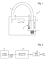
- FIG. 1 shows schematically a lock 2, represented in its closed state, equipped with an external event detection device which comprises a sensor 10 and an electronic unit 12 according to the present invention.
- the sensor is formed by a piezoelectric element and associated circuitry arranged for providing an electrical power signal to the electronic unit when a certain pressure is applied on the piezoelectric element.
- This electrical power signal will be named '(electrical) stimulus signal' in the present description of the invention.
- the sensor 10 defines an energy harvester according to the present invention. This sensor transforms energy from an external event applied on it into electrical energy contained in an electrical stimulus pulse that forms an electrical stimulus signal provided to the electronic unit.
- the aim of this detection device is to detect if a tamper event has occurred in a zone or in a case or container protected by this lock. If the lock is forced, i.e. tampered with, the spring 4 will push up the piece 6 and the spring 8 will apply a force on the piezoelectric element with at least a given strength or intensity. This external event is stored in a memory part of the detection device. Before opening the lock, an authorized user will have to first read the memory to know if a tamper event has occurred.
- FIG 2 shows the basic architecture of a first embodiment of the external event detection device according to the invention.
- the DC electrical energy of an external event is collected by the sensor forming an energy harvester 16 and provided to a memory part of the electronic unit, formed by a Non-Volatile Memory (NVM) unit 18 comprising at least one NVM cell, through an electrical stimulus signal line (set line).
- NVM Non-Volatile Memory
- set line an electrical stimulus signal line
- this energy is provided by the force applied by the spring 8 on the piezoelectric element of the sensor 10.
- the memory part 18 is arranged for storing at least a bit of information or an item of data relative to at least one external event detected by the external event sensor 16.
- the electronic unit is arranged for storing said data by substantially using only the electrical energy contained in the electrical stimulus pulse generated by the external event acting on the sensor.
- the detection device of Figure 2 defines a self-powered detection device. This is also the case for all other embodiments of the invention that will be further described.
- E s I sw ⁇ T sw ⁇ V sw
- I sw the switching current
- T sw the switching time
- the total electrical energy needed to store a bit of information or an item of data in one FET transistor is typically of the order of 10 nJ.
- the piezoelectric element "PIC 151 (ceramic PZT), sold by the German company Physik Instrumente (PI), can be used to produce the needed energy and voltage to set a flag in the NVM cell.
- PIC 151 ceramic PZT
- PI German company Physik Instrumente
- 10 nJ can be generated by such a piezoelectric element having a capacity C PZT of approximately 19 pF, with a voltage value of approximately 16 V across this Input capacitance, by applying a force of about 1.25 N on the piezoelectric element. It is possible to generate more than 10 nJ, for instance 20 nJ with such a piezoelectric element by increasing the applied force.
- a force amplifier can be arranged between the piezoelectric element and the spring (i.e. the element generating an external force used by the energy harvester when an external event occurs).
- a protection element or circuit can be added between the piezoelectric element and the electronic unit or in an input part of such an electronic unit.
- the electronic unit further comprises a readout circuit 20 allowing, when powered, the reading of the logical state of the NVM cell 18.
- the read circuit is only used during the reading phase (so only when the circuit is supplied).
- the read circuit is designed so that it will not interfere with the setting of the memory cell (whether the power supply is present or not).
- the read circuit will enable a read of the non-volatile memory cell and the output of the read circuit will return, e.g., a logical '0' if no tamper event occurred and a logical '1' if a tamper event has occurred. Since this circuit is here not resettable, it can detect only one tamper event.
- FIG. 3 shows a preferred electronic design of the previously described first embodiment.
- the non-volatile memory cell 24 is directly set to its written logical state from its initial logical state by an electrical stimulus pulse provided by the energy harvester (sensor) 16.
- the NVM cell 24 is formed by a first FET transistor T1 having a control gate, a source region SRC and a drain region DRN.
- the control gate is connected to a stimulus input of the electronic unit 22 receiving the electrical stimulus pulse/signal of said energy harvester.
- the ground of the electronic unit 22 is defined by the energy harvester / sensor which ground line (not represented) is connected to this electronic unit.
- the electronic unit 22 further comprises a set circuit 26 defining a switch arranged between the ground of the electronic unit and the drain DRN of the first FET transistor.
- This switch is preferably formed by a second FET transistor T2 having a control gate connected to the electrical stimulus input and is turned on when an electrical stimulus pulse is provided to the electronic unit, connecting the drain of the first FET transistor to ground (0 V) and thus allowing the secure setting of the non-volatile memory cell 24 to the logical '1' state.
- the electronic unit 22 comprises reading means of said non-volatile memory cell which is active only when supplied by a power source.
- This reading means is formed by a latch 28 having its input connected to the drain DRN of said first FET transistor and automatically providing at its output, when a power supply is applied by an external device / reader, a signal indicating the state of the NVM cell.
- FIG. 4 shows a second embodiment of the self-powered detection device according to the invention.
- This second embodiment also concerns a variant without reset and further comprises in the electronic unit a control circuit 30 and a third FET transistor T3 controlled by this control circuit and arranged between the ground of the electronic unit and the source of the first FET transistor.
- the control circuit also controls the latch so as to disconnect this latch from the drain of the memory transistor T1 when an electrical stimulus pulse is provided to the electrical stimulus input.
- Figure 5 shows the basic architecture of a third embodiment of the self-powered detection device according to the invention.
- the electronic unit comprises reset means for resetting the non-volatile memory cell.
- the electrical energy of the external event is collected at the electrical stimulus input of the electronic unit and, as in the previous embodiments, a corresponding data is written in the NVM cell 34.
- This NVM cell has a reset input receiving a reset signal from a reset circuit 32. This reset circuit needs to be power supplied for resetting the memory cell.
- the reset circuit When power is supplied is present, the reset circuit allows resetting the non-volatile memory cell after an external event has been detected and this cell set. This allows reuse of the external event detector after one detected external event.
- the detection device When the detection device is supplied following a tamper event, the read circuit will enable a read of the non-volatile memory cell and the read output will be a logical '1'. Once this tamper event has been acknowledged, the user can reset the non-volatile memory cell through the reset circuit 32.
- the reset circuit and the read circuit are only used when the detection device is supplied by a power source. These elements are preferably designed so that they will not interfere with the setting of the memory cell during a tamper event (whether the supply is present or not).
- FIG. 6 shows a preferred electronic design of the third embodiment.
- the reset circuit is formed by a control circuit 40 and a level shifter 42 receiving a High Voltage (HV).
- the level shifter is controlled by the control circuit 40.
- the level shifter can be formed by a high voltage inverter (CMOS Inverter).
- CMOS Inverter high voltage inverter
- the level shifter output is turned OFF (high impedance so that it is not driven), the latch output is driven high and the read output is driven high again.
- the latch will then also be reset by the voltage level of the drain of memory cell T1. Then, the power supply can be removed and the detection device is again reusable as a self-powered detection device.
- FIG. 7 shows the architecture of a fourth embodiment of the self-powered detection device according to the invention.
- This Figure 7 is a block diagram of a resettable external event detector with a multi-Bit One-Time-Programmable (OTP) back-up storage.
- OTP One-Time-Programmable
- the fourth embodiment is characterized in that the electronic unit further comprises a One-Time-Programmable memory (OTP Memory), a bit of which is automatically written when this electronic unit is powered and the non-volatile memory cell is in the written / tampered state.
- OTP Memory One-Time-Programmable memory
- the OTP memory 44 comprises several Bits (N Bits).
- the read circuit 20 provides at its output the logical state of the NVM cell 34.
- the set control circuit 46 determines if this logical state corresponds to a set state. If this is the case, the set control circuit will set a Bit of the N-Bit OTP memory 44 which is not already set.
- the Bits of the OTP memory are successively set each time the non-volatile memory cell is set after a reset action, until all Bits of this OTP memory are set.
- a Counter and Encoder circuit 48 counts the number of set Bits in the OTP memory and provides the result in a coded format.
- the OTP memory is set at the same time that the NVM memory is set by a detected external event.
- This variant however requires more energy in the electrical stimulus pulse.
- to automatically write the OTP memory only when the electronic unit is supplied is advantageous for the powerless detection device of the present invention.
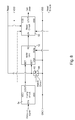
- Figure 8 show partially a general architecture of a self-powered detection device according to the present invention on the basis of which these further embodiments and variants will be described.
- the sensor / energy harvester is not represented in this Figure 8 , only two lines coming from such a sensor / energy harvester are shown. These two lines define two inputs of the electronic circuit of Figure 8 , of which the first one receives a voltage stimulus signal from the sensor when it is activated and the second one is connected to the ground (GND) of this sensor.
- GND ground
- These two inputs are those used in a detection mode of the self-powered detection device wherein no other supply source than the sensor is used for detecting at least one physical or chemical action or phenomenon applied to this sensor with at least a given strength or intensity, the electrical energy of an electrical stimulus pulse generated by such a physical or chemical action or phenomenon applied on the sensor being used.
- the voltage stimulus signal resulting from the electrical stimulus pulse is transferred to the electronic circuit of Figure 8 and used to set / write at least a NVM cell of the NVM unit 52.
- NVM unit 52 is arranged for storing in said NVM cell a bit of information relative to the detection by the sensor, during a detection mode of the self-powered detection device, of at least one physical or chemical action or phenomenon applied to it with at least a given strength or intensity and resulting in a voltage stimulus signal provided between a set control terminal SET and a base terminal SET * of the NVM unit 52 with at least a given set voltage.
- the detection device of Figure 8 comprises a read circuit 56 which is formed in a preferred variant by a latch already described.
- Clamp circuit 54 allows only a stimulus pulse with a predefined polarity to pass from its input CIN to its output COUT such that once a physical or chemical action or phenomenon, in particular a tamper event, is detected by the sensor, the record of this detection cannot be undone via the input CIN receiving the voltage stimulus signal.
- This protection is very interesting for tamper event detection because the input CIN, without such a clamp circuit, could be used by a tamperer for erasing the NVM cell, which has stored such a tamper event, by sending with an external device an electrical pulse with an inverse polarity relative to the polarity of the stimulus pulses generated by the sensor.
- the self-powered detection device of Figure 8 comprises a switch circuit 58 formed at least by a switch 60 arranged in the path between the ground GND of the sensor and the base terminal SET * of the NVM unit 52, the control gate G of this switch circuit being electrically connected to the set control terminal SET at least in the detection mode. It is to be noted that, in a variant not represented, the gate G of the switch circuit 58 can be disconnected from the SET terminal in other modes of the detection device (e.g. reset mode or read mode).
- the switch 60 is selected so as to be ON when the control gate G of the switch circuit 58 receives a voltage stimulus signal from the sensor with at least said given set voltage.
- the switch connects the base terminal SET * to GND (ground of the sensor) so that the voltage applied between the terminals SET and SET * of the NVM unit corresponds substantially to the whole voltage of the voltage stimulus signal, which ensures the setting of the at least one NVM cell in the NVM unit 52.
- the switch circuit is important for the detection device because it allows the implementation of further functions in an efficient way, in particular for reading the state of the NVM cell or for resetting it, where the base input SET * is used for such functions and must thus be disconnected from the ground of the sensor or the VSS terminal of a supply source intervening for such functions.
- the switch circuit 58 can in a variant be formed by a single switch element 60, in particular a transistor T2 as shown in Figures 3, 4 and 6 and already described.
- the switch 60 is also named 'transistor T2' or simply 'T2', but should not be interpreted as a limitation.
- the voltage stimulus signal is routed to input SET of the Non-Volatile Memory (NVM) unit 52.
- switch 60 / transistor T2 is turned on driving input SET * to the same potential as GND (OV).
- GND GND
- a NVM cell within the NVM unit 52 is then written to the "set" data state (flag).
- the input REN 'Read Enable' is driven high turning on a path for current to flow through output RD (Read output of the NVM unit).
- a high current represents one cell state of two possible cell states while a low current represents the other of the two cell states.
- the read circuit in particular a Latch as shown in Figures 3, 4 and 6 , senses the amount of current and drives output LOUT to either a logical one or a logical zero level.
- the input SET * of the NVM unit 52 is driven high under user control (through a reset circuit not shown) while COUT of the Clamp circuit 54 is driven low in order to put switch 60 (transistor T2) in its OFF state and thus to ensure that the SET * terminal is disconnected from GND, respectively from VSS of the power source.
- the switch circuit 58 is connected to GND of the sensor and also to VSS of a temporary power source used in the read mode and the reset mode. In a variant, this switch circuit is connected only to GND and not to VSS.
- FIG. 9 is an example implementation of a clamp circuit.
- Clamp A is a negative clamp, which prevents the stimulus input from going negative with respect to VSS by more than one diode voltage drop ( ⁇ 0.6V) with or without the device being supplied.
- a tamperer could allow a stimulus pulse to be emitted by the sensor to set the NVM cell (when this tamperer opens a protected device or enters a protected zone), extract information or material from the device / zone under protection or interfere with its operation, and then reset the NVM cell by applying a negative pulse of sufficient amplitude thereby removing any information that tampering occurred.
- the negative pulse could be provided from a pulse generator to the Set terminal after disconnecting the sensor from it. Then, the sensor could be reconnected.
- Clamp A is designed to prevent this type of intervention by a tamperer. Such a case thus especially concerns a detection device wherein the sensor circuit is not integrated with the NVM unit in a same integrated circuit.
- Clamp A is also a positive clamp. If the amplitude of the stimulus pulse is too high, then damage to transistors and other on-chip devices may occur.
- the diode of Clamp A is designed to break down shunting charge to VSS at a given positive voltage (V BREAKDOWN ) high enough to allow a set of the NVM cell but low enough to prevent damage. It is desirable that the diode be designed and laid out to pass the charge without itself being damaged.
- V BREAKDOWN positive voltage
- the Clamp A circuit 62 could in a different variant be formed by transistors controlled by the voltage stimulus signal in the detection mode, so as to perform the functions of Clamp A.
- Clamp B is a ground clamp. Its purpose is to drive COUT to the VSS level whenever CIN is approximately 0V.
- CIN can be at 0V potential if the sensor outputs 0V or if CIN is not driven or connected but discharges to 0V through a reverse-biased diode like D1 in Clamp A. It is desirable that a voltage stimulus signal can be applied at any time through it to the SET input. This would allow for tamper detection during read and reset operations.
- the SET input must be preferably at a stable, unalterable 0V level in order to ensure that a large enough voltage (VReset-min) can be developed to reset the NVM cell. If SET is not well-driven to 0V, then it may couple high due to parasitic coupling capacitance to high-going signals within the powered device, reducing the reset voltage below VReset-min. The same is true for a read operation in that SET must preferably be stable, unalterable, and 0V in order to provide a source of electrons for a read current or a known, stable voltage for a FET gate controlling read current.
- FIG 10 is a schematic diagram of an example implementation of the Clamp B subcircuit 64 of Figure 9 .
- V(VDD) is approximately 0V
- OUT is not driven by T10 or T11 if IN is low. No set operation occurs when IN is low. If an external event is detected and a stimulus pulse is applied to IN, then IN goes high turning on T12 causing node A to be driven low allowing T10 to turn on while T11 is off. Therefore, the stimulus pulse is passed to the SET terminal to set the NVM cell without a power supply for the device.
- a negative stimulus pulse applied to IN is clamped to a diode voltage drop by a diode existing between the N-well connection of T10 and the grounded p-type substrate preventing a reset of the NVM cell.
- a reset of the NVM cell is not possible through Clamp B by driving VDD negative because there exists a diode from N-well to grounded p-substrate that prevents VDD from going negative with respect to VSS by more than a diode drop.
- the same diode exists for PMOS devices elsewhere whose N-well is tied to VDD.
- An alternative to the Clamp B circuit of Figure 10 is an NMOS transistor with source connected to VSS, gate connected to a read or reset control signal from the VDD power domain, and drain connected to IN and OUT that also connects to Set.
- the disadvantage of this last circuit is that without device power a stimulus pulse may couple the gate high enabling a current path to VSS that degrades the stimulus pulse.
- Another disadvantage is that the stimulus pulse cannot be passed whenever a read or reset operation is being performed.
- Clamp B The functions of Clamp B are:
- a configuration with only Clamp A (without Clamp B) with preferably a large capacitor from SET to VSS can be functional enough for a NVFET cell with SET connected to the FET gate and for FeRAM NVM cells.
- a configuration with only Clamp B (without Clamp A) could be sufficient for preventing a tamperer to reset in particular a PCRAM NVM cell, if the breakdown of N-well to P+ drain of T10 is properly designed.
- the storage means consists of a field effect transistor (FET) containing charge storage material, collectively named Non-Volatile FET (NVFET).
- FET field effect transistor
- NVFET Non-Volatile FET
- FIG 11 is a diagram of a first embodiment of the NVM unit 52 of Figure 8 with a NVFET cell 72, where the stimulus pulse is applied to the control gate G of the NVFET.
- This NVFET comprises two diffusions defining its inputs 1 and 2.
- the stimulus pulse is routed via input SET to the Gate G of the NVFET cell.
- input SET * is driven low by switch 60 ( Figure 8 ), which in turn drives input 1 of the NVFET low.
- Subcircuit 68 'Isolation Crt A' isolates SET * from RD except during a read operation (read mode). Electrons are stored in the charge storage material causing the threshold voltage of NVFET to be high and current low during a read operation.
- SET * is driven high causing input 1 of NVFET 72 to be driven high.
- SET is driven low by subcircuit 64 'Clamp B' ( Figures 9 & 10 ) driving input G low and switching off the switch 60 ( Figure 8 ). Electrons tunnel out of the charge storage material leaving it positively charged, reducing its threshold voltage, and causing high current to flow during a read operation.
- Clamp B drives input SET low, which holds input G of NVFET 72 low, and the switch 60 ( Figure 8 ) is thus OFF.
- REN is high turning on T3 and T5 and thus connecting input 1 of the NVFET to output RD in order to allow current to flow for sensing by the read circuit (Latch circuit).
- the switch circuit 58 is essential in order to disconnect SET * from GND / VSS.
- the read output RD could, in a variant of this first embodiment, be connected to input 2 of the NVFET 72 while SET * is connected to input 1.
- inputs 1 and 2 in Figure 11 can be interchanged with the SET * terminal remaining connected to input 1.
- FIG 12 is a schematic diagram of an example of isolation subcircuit 68 (Isolation Crt A).
- Isolation Crt A isolation subcircuit 68
- transistor T4 is on and the gate of transistor T5 is connected to VSS.
- T5 is then turned off isolating IN and OUT.
- This isolation operation is possible with or without a supporting supply (VDD).
- REN which is in the VDD power supply domain, must be low or high-impedance (not driving) in order to not conflict with T4 driving the gate of T5 low.
- REN which is in the VDD power supply domain, must be low or high-impedance (not driving) in order to not conflict with T4 driving the gate of T5 low.
- REN is low, T5 is off isolating IN and OUT.
- ISO is low because SET is low via Clamp B ( Figures 9 & 10 ); REN is high causing T5 to turn on connecting OUT to IN, which allows current to flow.
- FIG 13 is a diagram of a second embodiment of the NVM unit 52 of Figure 8 with a NVFET cell 74 having a control gate G and two diffusions defining inputs 1 and 2, where a stimulus pulse is applied to one diffusion (Input 1) of the NVFET and where the read circuit senses, i.e. the read occurs, at the same diffusion / input.
- the stimulus pulse is routed through the subcircuit 76 'isolation Crt B' to input 1 of NVFET 74.
- SET * is driven low by transistor T2 (switch 60 of Figure 8 ), which in turn drives input G of the NVFET low.
- isolation subcircuits 68(1) and 68(2) isolate IN from OUT. Both subcircuits 68(1) and 68(2) correspond to the subcircuit 68 'Isolation Crt A' shown in Figure 12 .
- the isolation subcircuit 68(2) prevents any leakage current through NVFET 74 that may degrade the level of the stimulus pulse routed to the diffusion.
- the isolation subcircuit 68(1) isolates RD from input 1 of the NVFET also to prevent degradation of the stimulus pulse routed to the diffusion.
- SET is driven low by Clamp B ( Figures 9 & 10 ) and thus the switch 60 ( Figure 8 ) is OFF.
- SET * is driven high causing input G of NVFET 74 to be driven high.
- subcircuit 76 connects SET to input 1 of the NVFET, driving input 1 low. Electrons tunnel into the charge storage material leaving it negatively charged, raising its threshold voltage, and causing low current to flow during a read operation.
- the switch circuit 58 is essential in order to disconnect SET * from GND / VSS.
- SET * must hold input G of NVFET 74 low via the Reset line ( Figure 8 ).
- REN is high causing subcircuit 68(2) to connect input 2 of NVFET 74 to VSS in order to allow current to flow for sensing.
- Subcircuit 68(1) connects input 1 of NVFET to RD.
- Input REN causes subcircuit 76 'Isolation Crt B' to isolate SET, which is low, from input 1 of the NVFET.
- Figure 14 is a diagram of a variant of subcircuit 76 'isolation Crt B'.
- Input SET must not be connected to input 1 of NVFET during a read operation, but must pass to this input 1 the voltage stimulus signal during a set operation (detection mode without power supply) and 0V during a reset operation (with power supply).
- SET * low turns off T8; REN high turns off T6; and IN low turns off T7. Therefore, OUT is isolated from IN.
- the full voltage - preferably without threshold drop - must be passed from SET to input 1 of NVFET 74.
- SET * low which drives input EN *, turns off T8, and IN, which is driven by SET, is high what turns on T6 via T7.
- REN must be low or high-impedance (not driving) in order to not conflict with T7 driving the gate of T6 low. Therefore, a high level on SET forces IN to be connected to OUT.
- 0V During a reset operation, 0V must be passed from SET to input 1 of NVFET 74.
- SET * high turns on T8, EN low turns on T6, and IN, which is driven by SET, is low which turns off T7. Therefore, Clamp B ( Figures 9 & 10 ) drives SET low and 0V is passed from IN (input 1 of NVFET) to OUT.
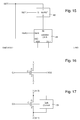
- FIG 15 is a diagram of a third embodiment of a NVM unit 52 ( Figure 8 ) with a NVFET 80 having a control gate G and two diffusions defining inputs 1 and 2, where a stimulus pulse is applied to one diffusion (input 1) of the NVFET and where the read occurs via the other diffusion (input 2) of this NVFET.
- the stimulus pulse is routed via input SET to input 1 of NVFET 80.
- SET * is driven low by transistor T2 (switch 60), which in turn drives input G of the NVFET low.
- the isolation subcircuit 68 isolates IN from OUT thus preventing any leakage current through the NVFET to output RD that may degrade the level of the stimulus pulse routed to the diffusion.
- SET is driven low by the Clamp circuit ( Figure 8 ), driving input 1 low, and thus switch 60 ( Figure 8 ) is OFF.
- SET * is driven high causing input G of NVFET 80 to be driven high. Electrons tunnel into the charge storage material leaving it negatively charged, raising its threshold voltage, and causing low current to flow during a read operation.
- the switch circuit 58 is essential in order to disconnect SET * from GND / VSS.
- a polysilicon gate is sandwiched between two oxide layers which are between a polysilicon gate and a single crystal silicon substrate.
- the floating gate stores electrons after a high field caused by high voltage induces tunneling. The tunneling can occur
- Electrons are stored in a nitride layer positioned similarly to a floating gate. Electrons tunnel through oxide above a channel zone.
- the drain D of the NVFET corresponds to input 1 ( Figures 11 , 13 and 15 ) and thus the source S corresponds to input 2. Because tunneling can occur anywhere along the channel for the second configuration ( Figure 17 ), inputs 1 and 2 ( Figures 11 , 13 and 15 ) may be interchanged. Thus, in the second configuration, input 1 can be the drain D or the source S of the NVFET. In this case, to erase the cell, the bulk must follow the drain and source to a high voltage and yet be connected to VSS while reading. This function requires a bulk connection control circuit 82 named 'Bulk Control'. There are well known circuits to perform this function.
- input 1 or 2 can be grounded in the detection mode for setting the NVFET and the resetting operation can occur through input 1 or 2, irrespective of which input is used for the setting operation.
Landscapes
- Electronic Switches (AREA)
- Storage Device Security (AREA)
Priority Applications (1)
| Application Number | Priority Date | Filing Date | Title |
|---|---|---|---|
| EP10191110.5A EP2325818B1 (de) | 2009-11-12 | 2010-11-12 | Stromversorgungsfreie Ereignisdetektionsvorrichtung |
Applications Claiming Priority (2)
| Application Number | Priority Date | Filing Date | Title |
|---|---|---|---|
| EP09175792 | 2009-11-12 | ||
| EP10191110.5A EP2325818B1 (de) | 2009-11-12 | 2010-11-12 | Stromversorgungsfreie Ereignisdetektionsvorrichtung |
Publications (2)
| Publication Number | Publication Date |
|---|---|
| EP2325818A1 true EP2325818A1 (de) | 2011-05-25 |
| EP2325818B1 EP2325818B1 (de) | 2016-04-06 |
Family
ID=42077538
Family Applications (2)
| Application Number | Title | Priority Date | Filing Date |
|---|---|---|---|
| EP10191110.5A Active EP2325818B1 (de) | 2009-11-12 | 2010-11-12 | Stromversorgungsfreie Ereignisdetektionsvorrichtung |
| EP10191111.3A Active EP2325819B1 (de) | 2009-11-12 | 2010-11-12 | Stromversorgungsfreie Ereignisdetektionsvorrichtung |
Family Applications After (1)
| Application Number | Title | Priority Date | Filing Date |
|---|---|---|---|
| EP10191111.3A Active EP2325819B1 (de) | 2009-11-12 | 2010-11-12 | Stromversorgungsfreie Ereignisdetektionsvorrichtung |
Country Status (2)
| Country | Link |
|---|---|
| US (1) | US20110110171A1 (de) |
| EP (2) | EP2325818B1 (de) |
Cited By (2)
| Publication number | Priority date | Publication date | Assignee | Title |
|---|---|---|---|---|
| US8422293B2 (en) | 2009-11-12 | 2013-04-16 | Em Microelectronic-Marin Sa | Self-powered event detection device |
| US8422317B2 (en) | 2009-11-12 | 2013-04-16 | Em Microelectronic-Marin Sa | Self-powered detection device with a non-volatile memory |
Families Citing this family (7)
| Publication number | Priority date | Publication date | Assignee | Title |
|---|---|---|---|---|
| US8411505B2 (en) * | 2009-11-12 | 2013-04-02 | Em Microelectronic-Marin Sa | Self-powered detection device with a non-volatile memory |
| EP2453424B1 (de) * | 2010-11-12 | 2014-02-26 | EM Microelectronic-Marin SA | Selbstversorgte Detektionsvorrichtung mit nichtflüchtigem Speicher |
| US9777510B2 (en) * | 2011-03-03 | 2017-10-03 | Assa Abloy Ab | Tamper switch activation without power |
| CN102831674B (zh) * | 2012-02-24 | 2014-10-08 | 浙江中烟工业有限责任公司 | 一种门锁死机开门装置 |
| US10141128B1 (en) * | 2017-11-10 | 2018-11-27 | Eaton Corporation | Method and apparatus for authenticating and detecting circuit breaker integrity |
| FR3094920B1 (fr) * | 2019-04-09 | 2021-10-01 | Ateq | Dispositif pour systeme electronique de controle de la pression des pneus d’un vehicule automobile. |
| US10784313B1 (en) | 2019-06-11 | 2020-09-22 | International Business Machines Corporation | Integrated resistive processing unit to avoid abrupt set of RRAM and abrupt reset of PCM |
Citations (4)
| Publication number | Priority date | Publication date | Assignee | Title |
|---|---|---|---|---|
| EP0592097A2 (de) | 1992-10-06 | 1994-04-13 | The Whitaker Corporation | Eindringdetektorsystem |
| WO1994010686A1 (en) * | 1992-11-02 | 1994-05-11 | Nvx Corporation | Flash memory system, and methods of constructing and utilizing same |
| US20020190610A1 (en) | 1999-12-16 | 2002-12-19 | Philippe Andre | Self-powered remote control device, electrical apparatus and installation comprising same |
| US20090073760A1 (en) * | 2007-09-17 | 2009-03-19 | Yoram Betser | Minimizing read disturb in an array flash cell |
Family Cites Families (3)
| Publication number | Priority date | Publication date | Assignee | Title |
|---|---|---|---|---|
| US5317303A (en) * | 1992-09-11 | 1994-05-31 | Anro Engineering, Inc. | Batteryless sensor used in security applications |
| JP4725979B2 (ja) * | 2005-07-15 | 2011-07-13 | 国立大学法人東北大学 | センサタグ、センサタグ装置、受電力回路、センサタグ装置の電力供給方法 |
| US20080174281A1 (en) * | 2005-09-05 | 2008-07-24 | Albert Shau | Electrical power generators |
-
2009
- 2009-11-17 US US12/620,365 patent/US20110110171A1/en not_active Abandoned
-
2010
- 2010-11-12 EP EP10191110.5A patent/EP2325818B1/de active Active
- 2010-11-12 EP EP10191111.3A patent/EP2325819B1/de active Active
Patent Citations (4)
| Publication number | Priority date | Publication date | Assignee | Title |
|---|---|---|---|---|
| EP0592097A2 (de) | 1992-10-06 | 1994-04-13 | The Whitaker Corporation | Eindringdetektorsystem |
| WO1994010686A1 (en) * | 1992-11-02 | 1994-05-11 | Nvx Corporation | Flash memory system, and methods of constructing and utilizing same |
| US20020190610A1 (en) | 1999-12-16 | 2002-12-19 | Philippe Andre | Self-powered remote control device, electrical apparatus and installation comprising same |
| US20090073760A1 (en) * | 2007-09-17 | 2009-03-19 | Yoram Betser | Minimizing read disturb in an array flash cell |
Non-Patent Citations (1)
| Title |
|---|
| CHAN T Y ET AL: "A TRUE SINGLE-TRANSISTOR OXIDE-NITRIDE-OXIDE EEPROM DEVICE", IEEE ELECTRON DEVICE LETTERS, IEEE SERVICE CENTER, NEW YORK, NY, US, vol. EDC-08, no. 3, 3 March 1987 (1987-03-03), pages 93 - 95, XP002047234, ISSN: 0741-3106 * |
Cited By (2)
| Publication number | Priority date | Publication date | Assignee | Title |
|---|---|---|---|---|
| US8422293B2 (en) | 2009-11-12 | 2013-04-16 | Em Microelectronic-Marin Sa | Self-powered event detection device |
| US8422317B2 (en) | 2009-11-12 | 2013-04-16 | Em Microelectronic-Marin Sa | Self-powered detection device with a non-volatile memory |
Also Published As
| Publication number | Publication date |
|---|---|
| US20110110171A1 (en) | 2011-05-12 |
| EP2325819A1 (de) | 2011-05-25 |
| EP2325818B1 (de) | 2016-04-06 |
| EP2325819B1 (de) | 2016-03-23 |
Similar Documents
| Publication | Publication Date | Title |
|---|---|---|
| US8422317B2 (en) | Self-powered detection device with a non-volatile memory | |
| EP2325818B1 (de) | Stromversorgungsfreie Ereignisdetektionsvorrichtung | |
| US8411505B2 (en) | Self-powered detection device with a non-volatile memory | |
| CN101611414B (zh) | 电子电路中的信息的保护 | |
| DE10305587B4 (de) | Integrierte Sicherheitshalbleiterschaltung und Halbleiterschaltungskarte und zugehöriges Überwachungsverfahren | |
| US6795347B2 (en) | Memory circuit | |
| SE462876B (sv) | Identifieringselement i form av en integrerad krets inkorporerad i identitetskort eller liknande databaerare | |
| TW201123354A (en) | Semiconductor integrated circuit and IC card system | |
| KR101108516B1 (ko) | 비휘발성 저장 장치와 방법 | |
| CN101595531A (zh) | 用于进行时间测量的电荷保持电路的编程 | |
| US5986284A (en) | Semiconductor device | |
| US8422293B2 (en) | Self-powered event detection device | |
| WO2008028129A2 (en) | Non-volatile memory cell in standard cmos process | |
| EP2453424B1 (de) | Selbstversorgte Detektionsvorrichtung mit nichtflüchtigem Speicher | |
| US7119703B2 (en) | Die anti-tampering sensor | |
| US6964378B2 (en) | Circuit for a focused ion beam (FIB) sensor | |
| US8254161B2 (en) | Device that can be rendered useless and method thereof | |
| US6795330B2 (en) | Method of reading and restoring data stored in a ferroelectric memory cell | |
| JP2020513567A (ja) | 静電気放電の回数を検出するための装置および方法 | |
| KR102119341B1 (ko) | 데이터 정보 유출 방지 솔리드 스테이트 드라이브 | |
| CN109844752B (zh) | 固态硬盘数据信息防泄漏安全装置 | |
| JP3725695B2 (ja) | 自己破壊型半導体装置 | |
| CN114503200B (zh) | 用于可靠并且安全的存储器擦除的方法和系统 | |
| US5926416A (en) | Electrically programmable non-volatile memory cells device for a reduced number of programming cycles | |
| WO2013040580A1 (en) | Percolation tamper protection circuit for electronic devices |
Legal Events
| Date | Code | Title | Description |
|---|---|---|---|
| PUAI | Public reference made under article 153(3) epc to a published international application that has entered the european phase |
Free format text: ORIGINAL CODE: 0009012 |
|
| AK | Designated contracting states |
Kind code of ref document: A1 Designated state(s): AL AT BE BG CH CY CZ DE DK EE ES FI FR GB GR HR HU IE IS IT LI LT LU LV MC MK MT NL NO PL PT RO RS SE SI SK SM TR |
|
| AX | Request for extension of the european patent |
Extension state: BA ME |
|
| 17P | Request for examination filed |
Effective date: 20111125 |
|
| REG | Reference to a national code |
Ref country code: DE Ref legal event code: R079 Ref document number: 602010032006 Country of ref document: DE Free format text: PREVIOUS MAIN CLASS: G08B0013060000 Ipc: E05B0039000000 |
|
| GRAP | Despatch of communication of intention to grant a patent |
Free format text: ORIGINAL CODE: EPIDOSNIGR1 |
|
| RIC1 | Information provided on ipc code assigned before grant |
Ipc: E05B 39/00 20060101AFI20151112BHEP |
|
| INTG | Intention to grant announced |
Effective date: 20151209 |
|
| RIN1 | Information on inventor provided before grant (corrected) |
Inventor name: KAMP, DAVID A. Inventor name: ROZ, THIERRY Inventor name: MARINELLI, FILIPPO |
|
| GRAS | Grant fee paid |
Free format text: ORIGINAL CODE: EPIDOSNIGR3 |
|
| GRAA | (expected) grant |
Free format text: ORIGINAL CODE: 0009210 |
|
| AK | Designated contracting states |
Kind code of ref document: B1 Designated state(s): AL AT BE BG CH CY CZ DE DK EE ES FI FR GB GR HR HU IE IS IT LI LT LU LV MC MK MT NL NO PL PT RO RS SE SI SK SM TR |
|
| REG | Reference to a national code |
Ref country code: GB Ref legal event code: FG4D |
|
| REG | Reference to a national code |
Ref country code: AT Ref legal event code: REF Ref document number: 788033 Country of ref document: AT Kind code of ref document: T Effective date: 20160415 Ref country code: CH Ref legal event code: EP |
|
| REG | Reference to a national code |
Ref country code: IE Ref legal event code: FG4D |
|
| REG | Reference to a national code |
Ref country code: DE Ref legal event code: R096 Ref document number: 602010032006 Country of ref document: DE |
|
| REG | Reference to a national code |
Ref country code: CH Ref legal event code: NV Representative=s name: ICB INGENIEURS CONSEILS EN BREVETS SA, CH |
|
| REG | Reference to a national code |
Ref country code: NL Ref legal event code: FP |
|
| REG | Reference to a national code |
Ref country code: LT Ref legal event code: MG4D |
|
| REG | Reference to a national code |
Ref country code: FR Ref legal event code: PLFP Year of fee payment: 7 |
|
| PG25 | Lapsed in a contracting state [announced via postgrant information from national office to epo] |
Ref country code: IS Free format text: LAPSE BECAUSE OF FAILURE TO SUBMIT A TRANSLATION OF THE DESCRIPTION OR TO PAY THE FEE WITHIN THE PRESCRIBED TIME-LIMIT Effective date: 20160806 Ref country code: NO Free format text: LAPSE BECAUSE OF FAILURE TO SUBMIT A TRANSLATION OF THE DESCRIPTION OR TO PAY THE FEE WITHIN THE PRESCRIBED TIME-LIMIT Effective date: 20160706 Ref country code: PL Free format text: LAPSE BECAUSE OF FAILURE TO SUBMIT A TRANSLATION OF THE DESCRIPTION OR TO PAY THE FEE WITHIN THE PRESCRIBED TIME-LIMIT Effective date: 20160406 Ref country code: LT Free format text: LAPSE BECAUSE OF FAILURE TO SUBMIT A TRANSLATION OF THE DESCRIPTION OR TO PAY THE FEE WITHIN THE PRESCRIBED TIME-LIMIT Effective date: 20160406 Ref country code: FI Free format text: LAPSE BECAUSE OF FAILURE TO SUBMIT A TRANSLATION OF THE DESCRIPTION OR TO PAY THE FEE WITHIN THE PRESCRIBED TIME-LIMIT Effective date: 20160406 |
|
| PG25 | Lapsed in a contracting state [announced via postgrant information from national office to epo] |
Ref country code: SE Free format text: LAPSE BECAUSE OF FAILURE TO SUBMIT A TRANSLATION OF THE DESCRIPTION OR TO PAY THE FEE WITHIN THE PRESCRIBED TIME-LIMIT Effective date: 20160406 Ref country code: ES Free format text: LAPSE BECAUSE OF FAILURE TO SUBMIT A TRANSLATION OF THE DESCRIPTION OR TO PAY THE FEE WITHIN THE PRESCRIBED TIME-LIMIT Effective date: 20160406 Ref country code: PT Free format text: LAPSE BECAUSE OF FAILURE TO SUBMIT A TRANSLATION OF THE DESCRIPTION OR TO PAY THE FEE WITHIN THE PRESCRIBED TIME-LIMIT Effective date: 20160808 Ref country code: GR Free format text: LAPSE BECAUSE OF FAILURE TO SUBMIT A TRANSLATION OF THE DESCRIPTION OR TO PAY THE FEE WITHIN THE PRESCRIBED TIME-LIMIT Effective date: 20160707 Ref country code: LV Free format text: LAPSE BECAUSE OF FAILURE TO SUBMIT A TRANSLATION OF THE DESCRIPTION OR TO PAY THE FEE WITHIN THE PRESCRIBED TIME-LIMIT Effective date: 20160406 Ref country code: RS Free format text: LAPSE BECAUSE OF FAILURE TO SUBMIT A TRANSLATION OF THE DESCRIPTION OR TO PAY THE FEE WITHIN THE PRESCRIBED TIME-LIMIT Effective date: 20160406 Ref country code: HR Free format text: LAPSE BECAUSE OF FAILURE TO SUBMIT A TRANSLATION OF THE DESCRIPTION OR TO PAY THE FEE WITHIN THE PRESCRIBED TIME-LIMIT Effective date: 20160406 |
|
| PG25 | Lapsed in a contracting state [announced via postgrant information from national office to epo] |
Ref country code: BE Free format text: LAPSE BECAUSE OF FAILURE TO SUBMIT A TRANSLATION OF THE DESCRIPTION OR TO PAY THE FEE WITHIN THE PRESCRIBED TIME-LIMIT Effective date: 20160406 Ref country code: IT Free format text: LAPSE BECAUSE OF FAILURE TO SUBMIT A TRANSLATION OF THE DESCRIPTION OR TO PAY THE FEE WITHIN THE PRESCRIBED TIME-LIMIT Effective date: 20160406 |
|
| REG | Reference to a national code |
Ref country code: DE Ref legal event code: R097 Ref document number: 602010032006 Country of ref document: DE |
|
| PG25 | Lapsed in a contracting state [announced via postgrant information from national office to epo] |
Ref country code: DK Free format text: LAPSE BECAUSE OF FAILURE TO SUBMIT A TRANSLATION OF THE DESCRIPTION OR TO PAY THE FEE WITHIN THE PRESCRIBED TIME-LIMIT Effective date: 20160406 Ref country code: EE Free format text: LAPSE BECAUSE OF FAILURE TO SUBMIT A TRANSLATION OF THE DESCRIPTION OR TO PAY THE FEE WITHIN THE PRESCRIBED TIME-LIMIT Effective date: 20160406 Ref country code: CZ Free format text: LAPSE BECAUSE OF FAILURE TO SUBMIT A TRANSLATION OF THE DESCRIPTION OR TO PAY THE FEE WITHIN THE PRESCRIBED TIME-LIMIT Effective date: 20160406 Ref country code: RO Free format text: LAPSE BECAUSE OF FAILURE TO SUBMIT A TRANSLATION OF THE DESCRIPTION OR TO PAY THE FEE WITHIN THE PRESCRIBED TIME-LIMIT Effective date: 20160406 Ref country code: SK Free format text: LAPSE BECAUSE OF FAILURE TO SUBMIT A TRANSLATION OF THE DESCRIPTION OR TO PAY THE FEE WITHIN THE PRESCRIBED TIME-LIMIT Effective date: 20160406 |
|
| PLBE | No opposition filed within time limit |
Free format text: ORIGINAL CODE: 0009261 |
|
| STAA | Information on the status of an ep patent application or granted ep patent |
Free format text: STATUS: NO OPPOSITION FILED WITHIN TIME LIMIT |
|
| PG25 | Lapsed in a contracting state [announced via postgrant information from national office to epo] |
Ref country code: SM Free format text: LAPSE BECAUSE OF FAILURE TO SUBMIT A TRANSLATION OF THE DESCRIPTION OR TO PAY THE FEE WITHIN THE PRESCRIBED TIME-LIMIT Effective date: 20160406 |
|
| 26N | No opposition filed |
Effective date: 20170110 |
|
| PG25 | Lapsed in a contracting state [announced via postgrant information from national office to epo] |
Ref country code: SI Free format text: LAPSE BECAUSE OF FAILURE TO SUBMIT A TRANSLATION OF THE DESCRIPTION OR TO PAY THE FEE WITHIN THE PRESCRIBED TIME-LIMIT Effective date: 20160406 |
|
| GBPC | Gb: european patent ceased through non-payment of renewal fee |
Effective date: 20161112 |
|
| REG | Reference to a national code |
Ref country code: IE Ref legal event code: MM4A |
|
| PG25 | Lapsed in a contracting state [announced via postgrant information from national office to epo] |
Ref country code: LU Free format text: LAPSE BECAUSE OF NON-PAYMENT OF DUE FEES Effective date: 20161130 |
|
| REG | Reference to a national code |
Ref country code: FR Ref legal event code: PLFP Year of fee payment: 8 |
|
| PG25 | Lapsed in a contracting state [announced via postgrant information from national office to epo] |
Ref country code: IE Free format text: LAPSE BECAUSE OF NON-PAYMENT OF DUE FEES Effective date: 20161112 Ref country code: GB Free format text: LAPSE BECAUSE OF NON-PAYMENT OF DUE FEES Effective date: 20161112 |
|
| PG25 | Lapsed in a contracting state [announced via postgrant information from national office to epo] |
Ref country code: CY Free format text: LAPSE BECAUSE OF FAILURE TO SUBMIT A TRANSLATION OF THE DESCRIPTION OR TO PAY THE FEE WITHIN THE PRESCRIBED TIME-LIMIT Effective date: 20160406 Ref country code: HU Free format text: LAPSE BECAUSE OF FAILURE TO SUBMIT A TRANSLATION OF THE DESCRIPTION OR TO PAY THE FEE WITHIN THE PRESCRIBED TIME-LIMIT; INVALID AB INITIO Effective date: 20101112 |
|
| PG25 | Lapsed in a contracting state [announced via postgrant information from national office to epo] |
Ref country code: MK Free format text: LAPSE BECAUSE OF FAILURE TO SUBMIT A TRANSLATION OF THE DESCRIPTION OR TO PAY THE FEE WITHIN THE PRESCRIBED TIME-LIMIT Effective date: 20160406 Ref country code: MC Free format text: LAPSE BECAUSE OF FAILURE TO SUBMIT A TRANSLATION OF THE DESCRIPTION OR TO PAY THE FEE WITHIN THE PRESCRIBED TIME-LIMIT Effective date: 20160406 Ref country code: TR Free format text: LAPSE BECAUSE OF FAILURE TO SUBMIT A TRANSLATION OF THE DESCRIPTION OR TO PAY THE FEE WITHIN THE PRESCRIBED TIME-LIMIT Effective date: 20160406 |
|
| PG25 | Lapsed in a contracting state [announced via postgrant information from national office to epo] |
Ref country code: BG Free format text: LAPSE BECAUSE OF FAILURE TO SUBMIT A TRANSLATION OF THE DESCRIPTION OR TO PAY THE FEE WITHIN THE PRESCRIBED TIME-LIMIT Effective date: 20160406 |
|
| PG25 | Lapsed in a contracting state [announced via postgrant information from national office to epo] |
Ref country code: MT Free format text: LAPSE BECAUSE OF NON-PAYMENT OF DUE FEES Effective date: 20161112 |
|
| REG | Reference to a national code |
Ref country code: FR Ref legal event code: PLFP Year of fee payment: 9 |
|
| PG25 | Lapsed in a contracting state [announced via postgrant information from national office to epo] |
Ref country code: AL Free format text: LAPSE BECAUSE OF FAILURE TO SUBMIT A TRANSLATION OF THE DESCRIPTION OR TO PAY THE FEE WITHIN THE PRESCRIBED TIME-LIMIT Effective date: 20160406 |
|
| REG | Reference to a national code |
Ref country code: AT Ref legal event code: UEP Ref document number: 788033 Country of ref document: AT Kind code of ref document: T Effective date: 20160406 |
|
| P01 | Opt-out of the competence of the unified patent court (upc) registered |
Effective date: 20230611 |
|
| PGFP | Annual fee paid to national office [announced via postgrant information from national office to epo] |
Ref country code: NL Payment date: 20251022 Year of fee payment: 16 |
|
| REG | Reference to a national code |
Ref country code: CH Ref legal event code: U11 Free format text: ST27 STATUS EVENT CODE: U-0-0-U10-U11 (AS PROVIDED BY THE NATIONAL OFFICE) Effective date: 20251201 |
|
| PGFP | Annual fee paid to national office [announced via postgrant information from national office to epo] |
Ref country code: DE Payment date: 20251022 Year of fee payment: 16 |
|
| PGFP | Annual fee paid to national office [announced via postgrant information from national office to epo] |
Ref country code: AT Payment date: 20251024 Year of fee payment: 16 |
|
| PGFP | Annual fee paid to national office [announced via postgrant information from national office to epo] |
Ref country code: FR Payment date: 20251022 Year of fee payment: 16 |
|
| PGFP | Annual fee paid to national office [announced via postgrant information from national office to epo] |
Ref country code: CH Payment date: 20251201 Year of fee payment: 16 |