EP2323217A1 - Antenne für eine Multimodus-MIMO-Kommunikation in tragbaren Vorrichtungen - Google Patents
Antenne für eine Multimodus-MIMO-Kommunikation in tragbaren Vorrichtungen Download PDFInfo
- Publication number
- EP2323217A1 EP2323217A1 EP09175974A EP09175974A EP2323217A1 EP 2323217 A1 EP2323217 A1 EP 2323217A1 EP 09175974 A EP09175974 A EP 09175974A EP 09175974 A EP09175974 A EP 09175974A EP 2323217 A1 EP2323217 A1 EP 2323217A1
- Authority
- EP
- European Patent Office
- Prior art keywords
- monopole
- antenna
- resonant frequency
- wireless communication
- substrate
- Prior art date
- Legal status (The legal status is an assumption and is not a legal conclusion. Google has not performed a legal analysis and makes no representation as to the accuracy of the status listed.)
- Granted
Links
- 238000004891 communication Methods 0.000 title claims description 73
- 230000005404 monopole Effects 0.000 claims abstract description 112
- 239000000758 substrate Substances 0.000 claims abstract description 56
- 230000005855 radiation Effects 0.000 claims abstract description 25
- 238000000034 method Methods 0.000 claims description 22
- 238000002955 isolation Methods 0.000 claims description 18
- 230000008878 coupling Effects 0.000 claims description 9
- 238000010168 coupling process Methods 0.000 claims description 9
- 238000005859 coupling reaction Methods 0.000 claims description 9
- 230000001413 cellular effect Effects 0.000 claims description 4
- 230000006870 function Effects 0.000 description 12
- 230000009977 dual effect Effects 0.000 description 7
- 238000010586 diagram Methods 0.000 description 6
- 238000006243 chemical reaction Methods 0.000 description 5
- 230000000875 corresponding effect Effects 0.000 description 5
- 230000005540 biological transmission Effects 0.000 description 3
- 238000009826 distribution Methods 0.000 description 3
- 230000010287 polarization Effects 0.000 description 3
- 238000003860 storage Methods 0.000 description 3
- 230000003321 amplification Effects 0.000 description 2
- 230000008859 change Effects 0.000 description 2
- 238000013461 design Methods 0.000 description 2
- 238000001914 filtration Methods 0.000 description 2
- 230000007774 longterm Effects 0.000 description 2
- 238000004519 manufacturing process Methods 0.000 description 2
- 239000000463 material Substances 0.000 description 2
- 238000003199 nucleic acid amplification method Methods 0.000 description 2
- 230000008569 process Effects 0.000 description 2
- 230000004044 response Effects 0.000 description 2
- PEZNEXFPRSOYPL-UHFFFAOYSA-N (bis(trifluoroacetoxy)iodo)benzene Chemical compound FC(F)(F)C(=O)OI(OC(=O)C(F)(F)F)C1=CC=CC=C1 PEZNEXFPRSOYPL-UHFFFAOYSA-N 0.000 description 1
- 238000012356 Product development Methods 0.000 description 1
- 230000004913 activation Effects 0.000 description 1
- 230000010267 cellular communication Effects 0.000 description 1
- 238000004590 computer program Methods 0.000 description 1
- 239000004020 conductor Substances 0.000 description 1
- 230000002596 correlated effect Effects 0.000 description 1
- 238000013500 data storage Methods 0.000 description 1
- 230000001419 dependent effect Effects 0.000 description 1
- 230000005520 electrodynamics Effects 0.000 description 1
- 238000011156 evaluation Methods 0.000 description 1
- 238000009434 installation Methods 0.000 description 1
- 238000002789 length control Methods 0.000 description 1
- 238000005259 measurement Methods 0.000 description 1
- 239000002184 metal Substances 0.000 description 1
- 230000003071 parasitic effect Effects 0.000 description 1
- 230000002085 persistent effect Effects 0.000 description 1
- 238000012545 processing Methods 0.000 description 1
- 230000005236 sound signal Effects 0.000 description 1
- 230000001360 synchronised effect Effects 0.000 description 1
Images


Classifications
-
- H—ELECTRICITY
- H01—ELECTRIC ELEMENTS
- H01Q—ANTENNAS, i.e. RADIO AERIALS
- H01Q1/00—Details of, or arrangements associated with, antennas
- H01Q1/12—Supports; Mounting means
- H01Q1/22—Supports; Mounting means by structural association with other equipment or articles
- H01Q1/24—Supports; Mounting means by structural association with other equipment or articles with receiving set
- H01Q1/241—Supports; Mounting means by structural association with other equipment or articles with receiving set used in mobile communications, e.g. GSM
- H01Q1/242—Supports; Mounting means by structural association with other equipment or articles with receiving set used in mobile communications, e.g. GSM specially adapted for hand-held use
- H01Q1/243—Supports; Mounting means by structural association with other equipment or articles with receiving set used in mobile communications, e.g. GSM specially adapted for hand-held use with built-in antennas
-
- H—ELECTRICITY
- H01—ELECTRIC ELEMENTS
- H01Q—ANTENNAS, i.e. RADIO AERIALS
- H01Q1/00—Details of, or arrangements associated with, antennas
- H01Q1/12—Supports; Mounting means
- H01Q1/22—Supports; Mounting means by structural association with other equipment or articles
- H01Q1/2283—Supports; Mounting means by structural association with other equipment or articles mounted in or on the surface of a semiconductor substrate as a chip-type antenna or integrated with other components into an IC package
-
- H—ELECTRICITY
- H01—ELECTRIC ELEMENTS
- H01Q—ANTENNAS, i.e. RADIO AERIALS
- H01Q1/00—Details of, or arrangements associated with, antennas
- H01Q1/36—Structural form of radiating elements, e.g. cone, spiral, umbrella; Particular materials used therewith
- H01Q1/38—Structural form of radiating elements, e.g. cone, spiral, umbrella; Particular materials used therewith formed by a conductive layer on an insulating support
-
- H—ELECTRICITY
- H01—ELECTRIC ELEMENTS
- H01Q—ANTENNAS, i.e. RADIO AERIALS
- H01Q21/00—Antenna arrays or systems
- H01Q21/28—Combinations of substantially independent non-interacting antenna units or systems
-
- H—ELECTRICITY
- H01—ELECTRIC ELEMENTS
- H01Q—ANTENNAS, i.e. RADIO AERIALS
- H01Q5/00—Arrangements for simultaneous operation of antennas on two or more different wavebands, e.g. dual-band or multi-band arrangements
-
- H—ELECTRICITY
- H01—ELECTRIC ELEMENTS
- H01Q—ANTENNAS, i.e. RADIO AERIALS
- H01Q5/00—Arrangements for simultaneous operation of antennas on two or more different wavebands, e.g. dual-band or multi-band arrangements
- H01Q5/30—Arrangements for providing operation on different wavebands
- H01Q5/307—Individual or coupled radiating elements, each element being fed in an unspecified way
- H01Q5/342—Individual or coupled radiating elements, each element being fed in an unspecified way for different propagation modes
- H01Q5/357—Individual or coupled radiating elements, each element being fed in an unspecified way for different propagation modes using a single feed point
- H01Q5/364—Creating multiple current paths
- H01Q5/371—Branching current paths
-
- H—ELECTRICITY
- H01—ELECTRIC ELEMENTS
- H01Q—ANTENNAS, i.e. RADIO AERIALS
- H01Q5/00—Arrangements for simultaneous operation of antennas on two or more different wavebands, e.g. dual-band or multi-band arrangements
- H01Q5/40—Imbricated or interleaved structures; Combined or electromagnetically coupled arrangements, e.g. comprising two or more non-connected fed radiating elements
-
- H—ELECTRICITY
- H01—ELECTRIC ELEMENTS
- H01Q—ANTENNAS, i.e. RADIO AERIALS
- H01Q9/00—Electrically-short antennas having dimensions not more than twice the operating wavelength and consisting of conductive active radiating elements
- H01Q9/04—Resonant antennas
- H01Q9/30—Resonant antennas with feed to end of elongated active element, e.g. unipole
- H01Q9/32—Vertical arrangement of element
- H01Q9/36—Vertical arrangement of element with top loading
Definitions
- the present invention relates to the field of communications systems, and, more particularly, to antennas for mobile wireless communications devices and related methods.
- Mobile devices are being required to support multiple applications, such as GSM, PSC, UMTS, WLAN, Wibro (Wireless broadband), and Bluetooth, and LTE, which in turn require multiple antennas, since one antenna cannot typically cover the bandwidth requirements of the multiple applications due to the physical limitations of an antenna described in " Physical Limitations of Antennas," IEEE Transactions on Antennas and Propagation, vol. 51, no. 8, pgs. 2116-2123, 2003 . As a result, multiple antennas must now share the already limited space within the mobile device.
- MIMO multiple-input multiple-out
- the antennas may be capable of covering as many bands as possible while being small in size and still having a high performance.
- a monopole antenna Compared to PIFA or IFA, a monopole can easier achieve large bandwidth because they may be arranged to radiate at two or more resonant frequencies (from its fundamental mode, second order and higher modes) Since a monopoles inherent dual mode characteristic makes it easy to achieve a frequency ratio of two-to-one of its upper and lower frequency band.
- the monopole may not cover all bands, such as GSM 900 (880 to 960 MHz) at a lower band and GSM1880/1900 and UMTS2100 (1710 to 2170 MHz) together at an upper band, unless additional parasitic branches are used to enhance the bandwidth and adjust the frequency ratio.
- GSM 900 880 to 960 MHz
- GSM1880/1900 GSM1880/1900
- UMTS2100 1710 to 2170 MHz
- Another disadvantage is that since a monopole is typically a quarter-wavelength of the fundamental mode, the size of the antenna is increased when it is designed to operate at lower resonant frequency bands.
- a monopole that may be arranged in a limited space.
- a multi-band antenna comprising a dielectric substrate, a ground plane formed on a first area of the dielectric substrate, a radiation part arranged on a second area of the dielectric substrate where the ground surface is not formed, a feed section formed of a metallic trace and having one end connected to the radiation part and an opposite end disposed near an edge of the ground plane for forming a feed point.
- the radiation part having a pair of monopole antenna elements formed of conductive metallic traces; a first monopole for radiating at a first resonant frequency, and a second monopole for radiating at a second resonant frequency and the conductive metallic traces being folded to form a three dimensional structure, with at least a portion of the first monopole spaced from a plane of the substrate and the second monopole.
- a patch element coupled to the second monopole and arranged in a spaced relationship to the first monopole, a width of the patch element for determining the resonant frequency of the second monopole antenna element, independently of the resonant frequency of the first monopole.
- dielectric shell defining a generally rectangular shape having opposing top and bottom faces, opposing first and second end faces and opposing first and second side faces, the bottom face of the dielectric shell positioned in the second area of the substrate and the three dimensional structure of the metallic trace being formed around the dielectric shell.
- a mobile wireless communication device comprising a housing, a dielectric substrate carried within the housing, wireless communication circuitry carried by the substrate within said housing, and a multi-band antenna coupled to the wireless communication circuitry and comprising a ground plane formed on a first area of the dielectric substrate, a radiation part arranged in a second area of the dielectric substrate where the ground surface is not formed, a feed section formed of a metallic trace and having one end connected to the radiation part and an opposite end disposed near an edge of the ground plane for forming a feed point; and the radiation part formed of conductive metallic traces; a first monopole for radiating at a first resonant frequency, and a second monopole for radiating at a second resonant frequency and the conductive metallic traces being folded to form a three dimensional structure, with at least a portion of the first monopole spaced from a plane of the substrate and the second monopole.
- a mobile wireless communication device comprising a housing, a dielectric substrate carried within said housing, wireless communication circuitry carried by the substrate, a ground plane formed on a first area of the dielectric substrate, a plurality multi-band antennas arranged in a second area of the dielectric substrate where the ground surface is not formed and coupled to said wireless communication circuitry, each of the multi-band antennas having a pair of monopole radiating elements including a patch element associated with respective ones of the multi-band antennas, a width of the patch element for determining a resonant frequency of its associated antenna.
- a stub section coupled to the ground plane and extending into the second area, a stub size being selected for determining an operating frequency and isolation of the multi-band antennas.
- a method for implementing a multi-band antenna for use in a mobile device comprising forming a ground plane in a first area of a dielectric substrate, the dielectric substrate for positioning within a housing of the mobile device; arranging a plurality of multi-band antennas in a second area of the dielectric substrate where the ground surface is not formed, the antennas for coupling to wireless communication circuitry, each of the multi-band antennas having a pair of monopole radiating elements including a patch element associated with respective ones of the multi-band antennas; and determining resonant frequency of respective antennas by adjusting a width of the patch element associated with that antenna.
- the method includes selecting a size of a stub section for extending the ground plane into the second area, for determining an operating frequency and isolation of the multi-band antennas.
- the present matter describes multi-band three-dimensional (3D) folded monopole antennas for use in mobile devices. More particularly the present matter describes a small compact multi-radiation element antenna that exhibits high mode isolation allowing it to cover several communication application frequency bands such as GSM 1900, UMTS2100, GPS, WALN in the 2GHz and higher range and the lower bands such as 1 GHz and wherein the operational frequency bands of antenna elements can be adjusted independently i.e. the upper bands can be adjusted independently of the lower bands. In other words the high mode isolation allows the antenna to function at different operation frequencies.
- 3D three-dimensional
- the multi-radiation element antenna also exhibits high isolation between the radiation elements. In other words there are low couplings (or power transferred from one element to another) at the operation frequencies of the antenna.
- the present matter describes a multi antenna array comprised of two or more of the multi-radiation element antennas, wherein the antennas of the array also exhibit high isolation.
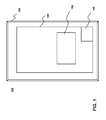
- a mobile wireless communications device 100 including a housing 102 , a substrate 104 carried within the housing, the substrate 104 having a ground plane (not shown) on one side thereof, wireless communications circuitry 106 carried within the housing 102 and located over the substrate 104 and a multi-band folded monopole antenna assembly 108 coupled to the wireless communications circuitry 106 .
- the wireless communications circuitry 106 may comprise cellular communications circuitry, e.g., a cellular transceiver.
- Other wireless communications circuitry such as wireless local area network (WLAN) and satellite positioning (e.g., GPS) communications circuitry, may also be used.
- WLAN wireless local area network
- GPS satellite positioning
- the antenna assembly 108 comprises a radiation part comprised of pair of monopoles formed of conductive metallic strips 110 folded into a 3D rectangular structure and located substantially on a top surface 105 and to one corner of the substrate 104 , as shown in FIG.
- a feed section 112 also located on the top surface 105 of the substrate connects the monopoles to a feed point 114 for coupling RF signals to and from the monopoles via a 50 ⁇ connector (not shown).
- a ground plane 116 is located on a bottom surface 107 in a first area 109 of the dielectric substrate 104 .
- the radiation part is arranged in a second area 115 of the dielectric substrate where the ground plane is not formed.
- the ground plane 116 is comprised of a metallic layer of polygonal shape having one edge delineating a boundary between the first area 109 and the second area 115 .
- the ground plane is rectangular, having a width (w) of 55mm and length (I) of 90mm and the substrate 104 is comprised of a 1.5 mm thick FR4 material with a dielectric constant of 4.4, having a width (W) of 55mm and length (L) of 105mm.
- the dimension of the substrate is usually constrained by the size of the mobile device housing.
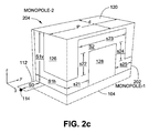
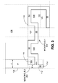
- the 3D geometrical configuration of the pair of folded monopoles is shown more clearly in FIG. 2c and FIG. 2d , and an unfolded two-dimensional (2D) view is shown in FIG. 3 .
- the pair of folded monopoles comprise a first and second monopole antenna elements monopole-1 202 and monople-2 204 formed of conductive metallic traces 110 , extending at right angles to each other, from the feed section 112 , the first monopole monopole-1 202 for radiating at a first resonant frequency, and the second monopole monople-2 204 for radiating at a second resonant frequency higher than the first frequency, and a patch element 120 coupled to the second monopole for determining the resonant frequency of the second monopole antenna element monople-2 204.
- the continuous metallic trace 110 is folded to take a generally rectangular shape and in an exemplary implementation is supported by a rectangular shaped dielectric shell 122 as shown more clearly in FIG. 2e .
- the dielectric shell 122 is mounted on a surface of the substrate 104 opposing the surface of the ground plane, referred to as the top surface 105 in FIG. 2a .
- the faces of the dielectric are referred to as opposing top 124 and bottom 125 faces in an x-y plane, opposing first 126 and second 127 end faces in an x-z plane, and opposing first 128 and second 129 side faces in the y-z plane.
- the bottom face 125 is formed by the substrate 104 .
- first monopole antenna element monopole-1 202 includes a continuous metallic trace comprised of the feed section S0 112 extending from the feed point 114 to a first horizontal section S1h arranged along a lower portion of the first end face 126 of the dielectric shell 122 to form a first L shaped section comprising S0 and S1h a first U-shaped section S2 on the first side face 128 , a second U-shaped section including a horizontal section S3 extending along a lower portion of the second end face 127 , a third U-shaped section S4 on the second side face 129 and ending in a second L-shaped section S5 on the bottom face 125 .
- the second monopole monopole-2 204 is composed of the feed section S0 , a vertical section S1v extending vertically along the first end face 126 and the patch P 120 formed on the top face 124 . It may be seen that the antenna is composed of three U- shaped sections formed generally of strips S2, S3 , and S4 and two L-shaped section formed of strips S1 and S5 .
- each monopole antenna element determines the antenna's performance
- the total length may be optimized taking into account the constraints on the volume for the antenna and the desired resonant frequency.
- the total length controls the fundamental resonating mode of the monopole elements, as will be appreciated by those skilled in the art.
- the modes at higher frequencies are generated at various portions of this length.
- the 3D wrapping of the antenna controls the current distribution along the monopole length, and thus controls the electrical length(s) for the higher resonant frequency band(s) as well as antenna bandwidth, as will also be appreciated by those skilled in the art.
- the initial electrical length of the first and second monopoles is set to a quarter of the wavelength of respective first and second resonant frequencies for the chosen fundamental modes.
- the fundamental mode is set at 1 GHz for the first monopole and 2 GHz for the second monopole.
- the geometric parameters may be optimized by using electromagnetic simulators such as those based on Finite-difference time-domain (FDTD) computational electrodynamics modeling techniques, as is known in the art. An example of which is a commercially available program by CST.
- FDTD Finite-difference time-domain
- the width d of the patch 120 varies the bandwidth and performance of the antenna.
- the width d of the patch 120 is set to 2mm, identical to the width of the other strips.
- the dielectric shell has dimensions of 14mm in length ( I1 ), 7mm in width ( w2 ) and 7.5mm in height ( h ). It is to be noted that the dielectric shell is mounted to the top surface of the substrate and thus the height of the dielectric shell is increased by 1.5 mm, the thickness of the substrate 104 .
- the above dimensions are for an exemplary embodiment; however, it will be appreciated by those skilled in the art that other dimensions and/or materials may be used in different embodiments.
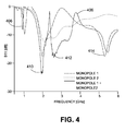
- FIG. 4 there is shown a comparison of simulated reflection coefficients for the antenna, having dimensions as above, when monopole-1 202 is excited on its own 402 ; monopole-2 204 is excited alone 404 , and the combined reflection coefficients when monopole-1 202 and monopole-2 204 are excited simultaneously 406 .
- the antenna exhibits four resonant frequencies of 0.95 GHz ( 408 ), 2 GHz ( 410 ), 2.5 GHz ( 412 ) and 5.4 GHz ( 414 ).
- the bandwidths and impedance matching at the frequencies of 0.95 GHz, 2 GHz and 5.4 GHz for the simultaneously excited monopoles are not significantly different. However at 2.5 GHz the bandwidth is significantly enhanced.
- one of the monopoles in this case the first monopole monopole-1 202, determines the bandwidths and resonant frequencies at 0.95 GHz, 2 GHz and 5.4 GHz bands, whereas the other monopole, in this case the second monopole monopole-2 204 , determines the bandwidth at the 2.5 GHz band.
- the first monopole monopole-1 202 operates at its fundamental mode and the total length of the first monopole monopole-1 202 is approximately a quarter wavelength.
- operation frequency is increased to 2 GHz
- the first monopole monopole-1 202 operates at the second-order mode of 2 GHz.
- the electrical length of the first monopole monopole-1 202 is a half wavelength.
- the antenna works at the higher order mode and its electrical length is more than one wavelength.
- the second monopole monopole-2 when it is excited alone at 2 GHz the currents also flow in a continuous direction, which means that the second monopole monopole-2 operates at the fundamental mode and its length is a quarter wavelength.
- the first monopole monopole-1 202 had strong surface currents while the second monopole monopole-2 204 exhibited weak surface currents. Accordingly, it can be inferred that the two monopoles have high-mode isolation, and that the first monopole monopole-1 202 primarily determines these resonant frequencies.
- the antenna operates at the 2.5 GHz band, the two monopoles exhibit strong surface currents, so they both have an influence in this band.
- the width d of the patch 120 changes the resonant frequency and bandwidth of the antenna.
- Another characteristic shown in FIG. 5 is that even by changing the patch width d and thereby varying a resonant frequency range, the antenna continues to be useful in a number of applicable frequency bands. In the exemplary implementation this ranges from 2 GHz to 4 GHz, which covers frequency bands applicable to GSM 1800/1900, UMTS2100, Blue-tooth 2.4 GHz, WiFi/LTE 2.6 GHz, WiMAX 3.3 to 3.8 GHz.
- RF-MEMS Radio-Frequency Micro-Electro-Mechanical System
- RF-MEMS Radio-Frequency Micro-Electro-Mechanical System
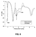
- FIG. 6 there is shown a comparison of a measured 602 and simulated 604 reflection coefficient S11 for an exemplary implementation, where the patch width d is 2 mm.
- the frequency range for the antenna is from 880 to 1000 MHz, which is within the frequency range for GSM 900 applications.
- the impedance bandwidth of 10 dB return loss is from 1700 MHz to 2820 MHz, which covers multiple applications at GSM /1800/1900 and UMTS 2100, long term evolution (LTE) 2.1 and 2.6 GHz bands.
- LTE long term evolution
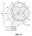
- FIGs. 7a-7d there is shown a logarithmic polar plot of measured far-field radiation patterns at resonant frequencies of 900 MHz ( FIG. 7a ), 1800 MHz ( FIG. 7b ), 2.5 GHz ( FIG. 7c ) and 5.5 GHz ( FIG. 7d ) of the exemplary implementation at the three planes of XOZ, YOZ and XOY, where the values are in units of dBi of gain.
- the orientation of the antenna for these measurements are the same as that of FIGs.
- the antenna peak gain ranges from -2 dBi to - 0.5 dBi at 900 MHz band, from 1.5 to 2.9 dBi at the middle frequency bands (1.7 to 2.17 GHz) and from 4 to 6 dBi at the high frequency band (4.9 to 6 GHz).
- These radiation patterns are omni-directional and dipole-like at 900 MHz ( FIG. 7a ), but the patterns are directive at 1800 MHz ( FIG. 7b ), 2.5 GHz ( FIG. 7c ) and 5.5 GHz ( FIG. 7d ).
- the total antenna efficiency was measured, which is defined as the ratio of the radiated power to the total power delivered to the input terminal of the antenna, i.e.
- the efficiency includes the impacts from mismatching loss, dielectric loss, and conductor loss.
- the antenna 108 achieved an efficiency of 50-75 % from 824 MHz to 960MHz, an efficiency of 58-85% from 1.6 GHz to 2.2 GHz and an efficiency of 50-75% from 4.9 to 6 GHz.
- FIG. 8a and 8b there is shown respective top and bottom perspective views of the 3D geometrical configuration of a multi-band 3D folded monopole antenna 808 according to another embodiment of the present matter.
- the antenna 808 is also located at a top of a PCB, having a feed point and feed section similar to antenna 108 .
- the antenna is positioned on the PCB and formed, in an exemplary embodiment, on a dielectric body 128 in a manner as previously described.
- the antenna 808 also comprises two monopole antenna elements, 810 and 812 formed on the dielectric shell illustrated in FIG 2e .
- the first monopole 810 is composed of a first folded monopole comprising a continuous metallic trace of uniform width comprising a feed section S0' extending from the feed point 114 to a vertical section and two roughly U-shaped sections S1', S2' formed on a first side face of the dielectric body.
- the U-shaped sections S1', S2 ' form a loop back to the feed section S0' .
- a second monopole 812 is composed of the feed section S0' , a section S4' extending vertically along the first end face, the top face, the second end face opposite the first end face of the dielectric body and ending in a patch P' formed on the bottom face of the substrate under the dielectric body.
- An L-shaped section S5 ' extends from the second end face section of the second monopole and is formed on the second side face opposite the first side face of the dielectric body.
- the patch P' in this embodiment is also spaced at distance h (the height of the dielectric body) from the first monopole. In this embodiment however one of the L-shaped sections (as described with respect to the embodiment of FIG. 2 ) is formed with the second monopole.
- the antenna response and performance are similar to the antenna 108 described earlier.
- the exemplary antennas provide a number of resonant frequencies within a desirable bandwidth in the frequency range of 2 GHz to 4 GHz by adjusting the patch width. This is useful when finalizing antenna designs because antenna adjustments are generally required at a late stage of product development. Typically large adjustments in the antennas dimensions are not feasible since the antenna's overall size has been fixed at the production stage.
- the antenna of the present matter can be easily adapted for used in mobile devices for reception of two or more unique radio signals, which require relatively low correlation between each of the received signals.
- FIG. 9a there is shown two-port antenna configurations 900 , as an example of a multi-port antenna, using a pair of folded monopole antennas 108 of the present matter.
- the antenna arrangement 900 includes a rectangular ground plane 901 as described earlier and a first 3D folded monopole antenna 902 and second 3D folded monopole antenna 904.
- the antennas are spaced apart and oriented 90 degrees with respect to each other in the second area 107 of the dielectric substrate where the ground plane 901 is not formed.
- a feed point 906 (port1) of the first antenna 902 is at one edge 905 of the ground plane 901 and a feed point 908 (port2) of the second antenna 904 is at a section of the ground plane 901 , which includes a section of metal that extends the ground plane, herein referred to as a stub 903 .
- the stub 903 extends from the edge 905 of the ground plane into the second area 107 and between the spaced apart antennas to end in proximity to the feed point 908 of the second antenna 904 .
- the stub 903 has a length of 17mm and a width of 10mm.
- FIG. 9b there is shown the two-port configuration comprised of antennas 808 and in FIG 9c there is shown the two-port configuration comprised of antennas 808 and 108 for the respective ports.
- Multi-port configurations can thus be built using one or more of the different pairs of monopole antennas described herein.
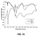
- plots of measured S parameters (S11, S21 and S22), for the dual port antennas, where S11 and S22 are reflection parameters and S21 is an isolation or coupling parameter.
- S11 and S22 are reflection parameters
- S21 is an isolation or coupling parameter.
- the dual-port antenna operates over multiple application bands, such as GSM/900/1800/1900, UMTS 2100 MHz bands, LTE 2.1/2.6 bands and WLAN 2.45/5 GHz bands, and the isolation between the two ports are better than - 13 dB across all bands from 500 MHz to 6 GHz.
- the isolation may be attributed to the two antennas having well implemented antenna diversities such as spatial, polarization and pattern diversity.
- the diversity techniques applied to the pair of antennas result in high isolation (low coupling) between the two ports.
- the two monopole antenna elements of each antenna are arranged vertically with respect to each other for polarization and pattern diversities, each of the dual antennas are separated for spatial diversity.
- Varying a size and arrangement of stub sections may change the response of the two-port antenna arrangement shown in FIGs. 9a -c .
- FIGs. 11a -b there is shown various stub sizes and arrangements for the two-port antenna 900 .
- a section 1102 is added along the edge 905 of the ground plane 901, to extend the ground plane under the second antenna 904 .
- the section 1102 has a width of 5 mm and length of 17mm and FIGs. 12a -c shown corresponding plots of measured S parameters (S11, S21 and S22, respectively), for the dual port antennas.
- FIG. 11b shows a further section 1104 added alongside one edge of the section 903 to extend the ground plane 901 between the antennas 902, 904.
- the section 1104 has a width of 10 mm and length of 17mm and FIGs. 13a -c show corresponding plots of measured S parameters (S11, S21 and S22, respectively).
- FIG. 11c there is shown a section 1106 added alongside the section 1104 to extend the ground plane 901 further between the antennas 902, 904 .
- the section 1106 has a width of 10 mm and length of 17mm, adding a width of 20 mm to the section 903 and
- FIGs. 14a-c show corresponding plots of measured S parameters (S11, S21 and S22, respectively).
- the size of the stub affects the operating frequency and isolation of the antennas 902, 904 .
- the size of the stub may be varied in order to change the overall operating frequency of the dual antenna arrangement.
- this may be combined with varying the patch width d of each multi-band antenna to provide a greater degree of flexibility in the operating range of the dual antenna.
- each antenna may be adjusted to operate in a particular frequency range without greatly affecting the other antenna. While the above embodiments have been described with respect to a dual antenna arrangement, arrangements with more than two antennas may also be implemented without departing from the scope of the present matter.
- Exemplary components of a hand-held mobile wireless communications device 2200 in which one or more of the above-described folded monopole antennas 108 may be used are now described with reference to FIG. 15 .
- the mobile device of FIG. 15 is not meant to be limiting, but merely provides an example of a mobile device that could be used in association with the present method and apparatus.
- Mobile device 2200 is preferably a two-way wireless communication device having at least voice and data communication capabilities. Mobile device 2200 preferably has the capability to communicate with other computer systems on the Internet. Depending on the exact functionality provided, the mobile device may be referred to as a data messaging device, a two-way pager, a wireless e-mail device, a cellular telephone with data messaging capabilities, a wireless Internet appliance, or a data communication device, as examples.
- mobile device 2200 is enabled for two-way communication, it will incorporate a communication subsystem 2211 , including a receiver 2212 and a transmitter 2214 , as well as associated components such as one or more, preferably embedded or internal, antenna elements 2216 and 2218 , local oscillators (LOs) 2213 , and a processing module such as a digital signal processor (DSP) 2220.
- LOs local oscillators
- DSP digital signal processor
- a GSM/UMTS device typically has a subscriber identity module (SIM) in order to get full service from the network.
- SIM subscriber identity module
- a cdma2000 device typically has such access credentials stored in it non-volatile memory or may use a removable user identity module (RUIM) in order to operate on a CDMA network.
- the SIM/RUIM interface 2244 is normally similar to a card-slot into which a SIM/RUIM card can be inserted and ejected like a diskette or PCMCIA card.
- the SIM/RUIM card can have approximately 64K of memory and hold many key configurations 2251 , and other information 2253 such as identification, and subscriber related information.
- mobile device 2200 may send and receive communication signals over the network 2219 .
- network 2219 can consist of multiple base stations communicating with the mobile device.
- Signals received by antenna 2216 through communication network 2219 are input to receiver 2212, which may perform such common receiver functions as signal amplification, frequency down conversion, filtering, channel selection and the like, and in the example system shown in FIG. 15 , analog to digital (A/D) conversion.
- A/D conversion of a received signal allows more complex communication functions such as demodulation and decoding to be performed in the DSP 2220 .
- signals to be transmitted are processed, including modulation and encoding for example, by the DSP 2220 and input to transmitter 2214 for digital to analog conversion, frequency up conversion, filtering, amplification and transmission over the communication network 2219 via antenna 2218 .
- the DSP 2220 not only processes communication signals, but also provides for receiver and transmitter control. For example, the gains applied to communication signals in receiver 2212 and transmitter 2214 may be adaptively controlled through automatic gain control algorithms implemented in the DSP 2220 .
- Mobile device 2200 preferably includes a microprocessor 2238 which controls the overall operation of the device. Communication functions, including at least data and voice communications, are performed through communication subsystem 2211 . Microprocessor 2238 also interacts with further device subsystems such as the display 2222 , flash memory 2224 , random access memory (RAM) 2226 , auxiliary input/output (I/O) subsystems 2228 , serial port 2230, two or more keyboards or keypads 2232 , speaker 2234, microphone 2236, other communication subsystem 2240 such as a short-range communications subsystem and any other device subsystems generally designated as 2242 Serial port 2230 could include a USB port or other port known to those in the art.
- RAM random access memory
- I/O auxiliary input/output subsystems 2228
- serial port 2230 two or more keyboards or keypads 2232
- speaker 2234 speaker 2234
- microphone 2236 other communication subsystem 2240
- Serial port 2230 could include a USB port or other port known to those in the art.
- Some of the subsystems shown in FIG. 15 perform communication-related functions, whereas other subsystems may provide "resident" or on-device functions.
- some subsystems such as keyboard 2232 and display 2222 , for example, may be used for both communication-related functions, such as entering a text message for transmission over a communication network, and device-resident functions such as a calculator or task list.
- Operating system software used by the microprocessor 2238 is preferably stored in a persistent store such as flash memory 2224 , which may instead be a read-only memory (ROM) or similar storage element (not shown).
- ROM read-only memory
- Those skilled in the art will appreciate that the operating system, specific device applications, or parts thereof, may be temporarily loaded into a volatile memory such as RAM 2226. Received communication signals may also be stored in RAM 2226 .
- flash memory 2224 can be segregated into different areas for both computer programs 2258 and program data storage 2250, 2252, 2254 and 2256. These different storage types indicate that each program can allocate a portion of flash memory 2224 for their own data storage requirements.
- Microprocessor 2238 in addition to its operating system functions, preferably enables execution of software applications on the mobile device. A predetermined set of applications that control basic operations, including at least data and voice communication applications for example, will normally be installed on mobile device 2200 during manufacturing. Other applications could be installed subsequently or dynamically.
- a preferred software application may be a personal information manager (PIM) application having the ability to organize and manage data items relating to the user of the mobile device such as, but not limited to, e-mail, calendar events, voice mails, appointments, and task items.
- PIM personal information manager
- Such PIM application would preferably have the ability to send and receive data items, via the wireless network 2219 .
- the PIM data items are seamlessly integrated, synchronized and updated, via the wireless network 2219 , with the mobile device user's corresponding data items stored or associated with a host computer system.
- Further applications may also be loaded onto the mobile device 2200 through the network 2219 , an auxiliary I/O subsystem 2228, serial port 2230 , short-range communications subsystem 2240 or any other suitable subsystem 2242 , and installed by a user in the RAM 2226 or preferably a non-volatile store (not shown) for execution by the microprocessor 2238 .
- Such flexibility in application installation increases the functionality of the device and may provide enhanced on-device functions, communication-related functions, or both.
- secure communication applications may enable electronic commerce functions and other such financial transactions to be performed using the mobile device 2200 .
- a received signal such as a text message or web page download will be processed by the communication subsystem 2211 and input to the microprocessor 2238 , which preferably further processes the received signal for output to the display 2222 , or alternatively to an auxiliary I/O device 2228 .
- a user of mobile device 2200 may also compose data items such as email messages for example, using the keyboard 2232 , which is preferably a complete alphanumeric keyboard or telephone-type keypad, in conjunction with the display 2222 and possibly an auxiliary I/O device 2228 . Such composed items may then be transmitted over a communication network through the communication subsystem 2211 .
- mobile device 2200 For voice communications, overall operation of mobile device 2200 is similar, except that received signals would preferably be output to a speaker 2234 and a microphone 2236 would generate signals for transmission.
- Alternative voice or audio I/O subsystems such as a voice message recording subsystem, may also be implemented on mobile device 2200 .
- voice or audio signal output is preferably accomplished primarily through the speaker 2234
- display 2222 may also be used to provide an indication of the identity of a calling party, the duration of a voice call, or other voice call related information for example.
- Serial port 2230 in FIG . 15 would normally be implemented in a personal digital assistant (PDA)-type mobile device for which synchronization with a user's desktop computer (not shown) may be desirable, but is an optional device component.
- PDA personal digital assistant
- Such a port 2230 would enable a user to set preferences through an external device or software application and would extend the capabilities of mobile device 2200 by providing for information or software downloads to mobile device 2200 other than through a wireless communication network.
- the alternate download path may for example be used to load an encryption key onto the device through a direct and thus reliable and trusted connection to thereby enable secure device communication.
- serial port 2230 can further be used to connect the mobile device to a computer to act as a modem.
- Other communications subsystems 2240 such as a short-range communications subsystem, is a further optional component which may provide for communication between mobile device 2200 and different systems or devices, which need not necessarily be similar devices.
- the subsystem 2240 may include an infrared device and associated circuits and components or a BluetoothTM communication module to provide for communication with similarly enabled systems and devices.
Landscapes
- Engineering & Computer Science (AREA)
- Physics & Mathematics (AREA)
- Electromagnetism (AREA)
- Microelectronics & Electronic Packaging (AREA)
- Computer Networks & Wireless Communication (AREA)
- Waveguide Aerials (AREA)
- Details Of Aerials (AREA)
- Variable-Direction Aerials And Aerial Arrays (AREA)
Priority Applications (3)
| Application Number | Priority Date | Filing Date | Title |
|---|---|---|---|
| EP09175974.6A EP2323217B1 (de) | 2009-11-13 | 2009-11-13 | Antenne für eine Multimodus-MIMO-Kommunikation in tragbaren Vorrichtungen |
| PCT/CA2010/001784 WO2011057398A1 (en) | 2009-11-13 | 2010-11-10 | Antenna for multi mode mimo communication in handheld devices |
| CA2776339A CA2776339C (en) | 2009-11-13 | 2010-11-10 | Antenna for multi mode mimo communication in handheld devices |
Applications Claiming Priority (1)
| Application Number | Priority Date | Filing Date | Title |
|---|---|---|---|
| EP09175974.6A EP2323217B1 (de) | 2009-11-13 | 2009-11-13 | Antenne für eine Multimodus-MIMO-Kommunikation in tragbaren Vorrichtungen |
Publications (2)
| Publication Number | Publication Date |
|---|---|
| EP2323217A1 true EP2323217A1 (de) | 2011-05-18 |
| EP2323217B1 EP2323217B1 (de) | 2014-04-30 |
Family
ID=41719314
Family Applications (1)
| Application Number | Title | Priority Date | Filing Date |
|---|---|---|---|
| EP09175974.6A Active EP2323217B1 (de) | 2009-11-13 | 2009-11-13 | Antenne für eine Multimodus-MIMO-Kommunikation in tragbaren Vorrichtungen |
Country Status (3)
| Country | Link |
|---|---|
| EP (1) | EP2323217B1 (de) |
| CA (1) | CA2776339C (de) |
| WO (1) | WO2011057398A1 (de) |
Cited By (6)
| Publication number | Priority date | Publication date | Assignee | Title |
|---|---|---|---|---|
| EP3285333A1 (de) * | 2016-08-16 | 2018-02-21 | Institut Mines Telecom / Telecom Bretagne | Konfigurierbare mehrbandantennenanordnung und entwurfsverfahren dafür |
| EP3386032A4 (de) * | 2015-12-29 | 2019-01-02 | Huawei Technologies Co., Ltd. | Antenne und kommunikationsvorrichtung |
| CN109149067A (zh) * | 2018-08-03 | 2019-01-04 | 瑞声精密制造科技(常州)有限公司 | 天线系统及移动终端 |
| CN109659687A (zh) * | 2019-01-23 | 2019-04-19 | 杭州电子科技大学 | 一种适用于5g移动终端的六单元多频段mimo天线 |
| CN112335120A (zh) * | 2018-06-29 | 2021-02-05 | 上海诺基亚贝尔股份有限公司 | 多频带天线结构 |
| WO2022059445A1 (ja) * | 2020-09-15 | 2022-03-24 | 株式会社村田製作所 | アンテナ装置 |
Families Citing this family (1)
| Publication number | Priority date | Publication date | Assignee | Title |
|---|---|---|---|---|
| CN113839200A (zh) * | 2021-10-09 | 2021-12-24 | 北京悦米科技有限公司 | 一种克服手握影响、受环境影响小的天线 |
Citations (7)
| Publication number | Priority date | Publication date | Assignee | Title |
|---|---|---|---|---|
| DE10049845A1 (de) * | 2000-10-09 | 2002-04-11 | Philips Corp Intellectual Pty | Mehrband-Mikrowellenantenne |
| JP2002158529A (ja) | 2000-11-20 | 2002-05-31 | Murata Mfg Co Ltd | 表面実装型アンテナ構造およびそれを備えた通信機 |
| US20030001781A1 (en) * | 2001-06-29 | 2003-01-02 | Takayoshi Konishi | Antenna element with conductors formed on outer surfaces of device substrate |
| EP1298760A1 (de) * | 2001-09-29 | 2003-04-02 | Philips Corporate Intellectual Property GmbH | Miniaturisierte Richtantenne |
| US20040125030A1 (en) * | 2002-12-16 | 2004-07-01 | Sung Jae Suk | Wireless LAN antenna and wireless LAN card with the same |
| US20040130495A1 (en) * | 2000-10-09 | 2004-07-08 | Achim Hilgers | Miniaturized microwave antenna |
| JP2005210523A (ja) | 2004-01-23 | 2005-08-04 | Kyocera Corp | 多周波表面実装アンテナとそれを用いたアンテナ装置ならびに無線通信装置 |
Family Cites Families (3)
| Publication number | Priority date | Publication date | Assignee | Title |
|---|---|---|---|---|
| US7719470B2 (en) * | 2007-08-23 | 2010-05-18 | Research In Motion Limited | Multi-band antenna, and associated methodology, for a radio communication device |
| EP2031695A1 (de) * | 2007-08-30 | 2009-03-04 | Research In Motion Limited | Mobile und drahtlose Kommunikationsvorrichtung mit gefalteter Multiband-Monopolantenne und entsprechende Verfahren |
| EP2034555B1 (de) * | 2007-09-06 | 2011-01-19 | Research In Motion Limited | Mobile drahtlose Kommunikationsvorrichtung mit mehrfach gewundener gefalteter Monopolantenne und entsprechende Verfahren |
-
2009
- 2009-11-13 EP EP09175974.6A patent/EP2323217B1/de active Active
-
2010
- 2010-11-10 WO PCT/CA2010/001784 patent/WO2011057398A1/en active Application Filing
- 2010-11-10 CA CA2776339A patent/CA2776339C/en active Active
Patent Citations (7)
| Publication number | Priority date | Publication date | Assignee | Title |
|---|---|---|---|---|
| DE10049845A1 (de) * | 2000-10-09 | 2002-04-11 | Philips Corp Intellectual Pty | Mehrband-Mikrowellenantenne |
| US20040130495A1 (en) * | 2000-10-09 | 2004-07-08 | Achim Hilgers | Miniaturized microwave antenna |
| JP2002158529A (ja) | 2000-11-20 | 2002-05-31 | Murata Mfg Co Ltd | 表面実装型アンテナ構造およびそれを備えた通信機 |
| US20030001781A1 (en) * | 2001-06-29 | 2003-01-02 | Takayoshi Konishi | Antenna element with conductors formed on outer surfaces of device substrate |
| EP1298760A1 (de) * | 2001-09-29 | 2003-04-02 | Philips Corporate Intellectual Property GmbH | Miniaturisierte Richtantenne |
| US20040125030A1 (en) * | 2002-12-16 | 2004-07-01 | Sung Jae Suk | Wireless LAN antenna and wireless LAN card with the same |
| JP2005210523A (ja) | 2004-01-23 | 2005-08-04 | Kyocera Corp | 多周波表面実装アンテナとそれを用いたアンテナ装置ならびに無線通信装置 |
Cited By (12)
| Publication number | Priority date | Publication date | Assignee | Title |
|---|---|---|---|---|
| EP3386032A4 (de) * | 2015-12-29 | 2019-01-02 | Huawei Technologies Co., Ltd. | Antenne und kommunikationsvorrichtung |
| US10734720B2 (en) | 2015-12-29 | 2020-08-04 | Huawei Technologies Co., Ltd. | Antenna and communications device |
| EP3285333A1 (de) * | 2016-08-16 | 2018-02-21 | Institut Mines Telecom / Telecom Bretagne | Konfigurierbare mehrbandantennenanordnung und entwurfsverfahren dafür |
| US10879612B2 (en) | 2016-08-16 | 2020-12-29 | Institut Mines-Telecom/Telecom Bretagne | Configurable multiband antenna arrangement and design method thereof |
| CN112335120A (zh) * | 2018-06-29 | 2021-02-05 | 上海诺基亚贝尔股份有限公司 | 多频带天线结构 |
| US11682838B2 (en) | 2018-06-29 | 2023-06-20 | Nokia Shanghai Bell Co., Ltd. | Multiband antenna structure |
| CN112335120B (zh) * | 2018-06-29 | 2023-09-19 | 上海诺基亚贝尔股份有限公司 | 多频带天线结构 |
| CN109149067A (zh) * | 2018-08-03 | 2019-01-04 | 瑞声精密制造科技(常州)有限公司 | 天线系统及移动终端 |
| CN109149067B (zh) * | 2018-08-03 | 2021-07-06 | 瑞声精密制造科技(常州)有限公司 | 天线系统及移动终端 |
| CN109659687A (zh) * | 2019-01-23 | 2019-04-19 | 杭州电子科技大学 | 一种适用于5g移动终端的六单元多频段mimo天线 |
| WO2022059445A1 (ja) * | 2020-09-15 | 2022-03-24 | 株式会社村田製作所 | アンテナ装置 |
| JP7359314B2 (ja) | 2020-09-15 | 2023-10-11 | 株式会社村田製作所 | アンテナ装置 |
Also Published As
| Publication number | Publication date |
|---|---|
| CA2776339A1 (en) | 2011-05-19 |
| EP2323217B1 (de) | 2014-04-30 |
| CA2776339C (en) | 2014-10-21 |
| WO2011057398A1 (en) | 2011-05-19 |
Similar Documents
| Publication | Publication Date | Title |
|---|---|---|
| US8754814B2 (en) | Antenna for multi mode MIMO communication in handheld devices | |
| RU2627010C1 (ru) | Многоантенная система и мобильный терминал | |
| KR100831753B1 (ko) | 다이버시티 안테나 장치 | |
| US6650294B2 (en) | Compact broadband antenna | |
| JP4384102B2 (ja) | 携帯無線機およびアンテナ装置 | |
| Bhatti et al. | Quad-band MIMO antenna array for portable wireless communications terminals | |
| EP1453137A1 (de) | Antenne für tragbares Funkgeraet | |
| CA2776339C (en) | Antenna for multi mode mimo communication in handheld devices | |
| EP2449624B1 (de) | Vorrichtung für drahtlose kommunikation mit einer schleifenartigen antenne | |
| US20090273529A1 (en) | Multiple antenna arrangement | |
| US7800546B2 (en) | Mobile wireless communications device including multi-loop folded monopole antenna and related methods | |
| KR20110043637A (ko) | 컴팩트 멀티밴드 안테나 | |
| CN112689033B (zh) | 终端设备 | |
| CA2638104C (en) | Mobile wireless communications device including multi-loop folded monopole antenna and related methods | |
| JP4473825B2 (ja) | 携帯端末用アンテナ | |
| EP2375488B1 (de) | Planarantenne und tragbare Vorrichtung | |
| US10374311B2 (en) | Antenna for a portable communication device | |
| Thavakumar et al. | Design of multi resonant PIFA antenna for mobile telecommunication networks | |
| Kaur et al. | 4-Elements MIMO System Integrated with Planar Monopole and Slot Antenna for Wireless Applications | |
| KR102253312B1 (ko) | 다중 대역 안테나 설계방법 및 장치, 그에 따른 다중 대역 안테나 | |
| Luo et al. | Low cost compact multiband printed monopole antennas and arrays for wireless communications | |
| Syrytsin et al. | Pattern-reconfigurable mobile terminal antenna system for MIMO and link stabilization in LTE | |
| Ma et al. | Pattern reconfigurable MIMO antennas for Multiband LTE Operation | |
| Rayene | DESIGN AND SIMULATION OF USB DONGLE ANTENNA | |
| WO2007011191A1 (en) | Small monopole antenna having loop element included feeder |
Legal Events
| Date | Code | Title | Description |
|---|---|---|---|
| PUAI | Public reference made under article 153(3) epc to a published international application that has entered the european phase |
Free format text: ORIGINAL CODE: 0009012 |
|
| 17P | Request for examination filed |
Effective date: 20091113 |
|
| AK | Designated contracting states |
Kind code of ref document: A1 Designated state(s): AT BE BG CH CY CZ DE DK EE ES FI FR GB GR HR HU IE IS IT LI LT LU LV MC MK MT NL NO PL PT RO SE SI SK SM TR |
|
| 17Q | First examination report despatched |
Effective date: 20111018 |
|
| RAP1 | Party data changed (applicant data changed or rights of an application transferred) |
Owner name: BLACKBERRY LIMITED |
|
| GRAP | Despatch of communication of intention to grant a patent |
Free format text: ORIGINAL CODE: EPIDOSNIGR1 |
|
| RAP1 | Party data changed (applicant data changed or rights of an application transferred) |
Owner name: BLACKBERRY LIMITED |
|
| RIC1 | Information provided on ipc code assigned before grant |
Ipc: H01Q 1/38 20060101ALI20131107BHEP Ipc: H01Q 5/00 20060101ALI20131107BHEP Ipc: H01Q 1/24 20060101AFI20131107BHEP Ipc: H01Q 9/36 20060101ALI20131107BHEP Ipc: H01Q 1/22 20060101ALI20131107BHEP Ipc: H01Q 21/28 20060101ALI20131107BHEP |
|
| INTG | Intention to grant announced |
Effective date: 20131121 |
|
| GRAS | Grant fee paid |
Free format text: ORIGINAL CODE: EPIDOSNIGR3 |
|
| GRAA | (expected) grant |
Free format text: ORIGINAL CODE: 0009210 |
|
| AK | Designated contracting states |
Kind code of ref document: B1 Designated state(s): AT BE BG CH CY CZ DE DK EE ES FI FR GB GR HR HU IE IS IT LI LT LU LV MC MK MT NL NO PL PT RO SE SI SK SM TR |
|
| REG | Reference to a national code |
Ref country code: GB Ref legal event code: FG4D Ref country code: CH Ref legal event code: EP |
|
| REG | Reference to a national code |
Ref country code: AT Ref legal event code: REF Ref document number: 665659 Country of ref document: AT Kind code of ref document: T Effective date: 20140515 |
|
| REG | Reference to a national code |
Ref country code: IE Ref legal event code: FG4D |
|
| REG | Reference to a national code |
Ref country code: DE Ref legal event code: R096 Ref document number: 602009023647 Country of ref document: DE Effective date: 20140612 |
|
| REG | Reference to a national code |
Ref country code: AT Ref legal event code: MK05 Ref document number: 665659 Country of ref document: AT Kind code of ref document: T Effective date: 20140430 |
|
| REG | Reference to a national code |
Ref country code: LT Ref legal event code: MG4D |
|
| REG | Reference to a national code |
Ref country code: NL Ref legal event code: VDEP Effective date: 20140430 |
|
| PG25 | Lapsed in a contracting state [announced via postgrant information from national office to epo] |
Ref country code: CY Free format text: LAPSE BECAUSE OF FAILURE TO SUBMIT A TRANSLATION OF THE DESCRIPTION OR TO PAY THE FEE WITHIN THE PRESCRIBED TIME-LIMIT Effective date: 20140430 Ref country code: NO Free format text: LAPSE BECAUSE OF FAILURE TO SUBMIT A TRANSLATION OF THE DESCRIPTION OR TO PAY THE FEE WITHIN THE PRESCRIBED TIME-LIMIT Effective date: 20140730 Ref country code: GR Free format text: LAPSE BECAUSE OF FAILURE TO SUBMIT A TRANSLATION OF THE DESCRIPTION OR TO PAY THE FEE WITHIN THE PRESCRIBED TIME-LIMIT Effective date: 20140731 Ref country code: IS Free format text: LAPSE BECAUSE OF FAILURE TO SUBMIT A TRANSLATION OF THE DESCRIPTION OR TO PAY THE FEE WITHIN THE PRESCRIBED TIME-LIMIT Effective date: 20140830 Ref country code: LT Free format text: LAPSE BECAUSE OF FAILURE TO SUBMIT A TRANSLATION OF THE DESCRIPTION OR TO PAY THE FEE WITHIN THE PRESCRIBED TIME-LIMIT Effective date: 20140430 Ref country code: BG Free format text: LAPSE BECAUSE OF FAILURE TO SUBMIT A TRANSLATION OF THE DESCRIPTION OR TO PAY THE FEE WITHIN THE PRESCRIBED TIME-LIMIT Effective date: 20140730 Ref country code: FI Free format text: LAPSE BECAUSE OF FAILURE TO SUBMIT A TRANSLATION OF THE DESCRIPTION OR TO PAY THE FEE WITHIN THE PRESCRIBED TIME-LIMIT Effective date: 20140430 Ref country code: NL Free format text: LAPSE BECAUSE OF FAILURE TO SUBMIT A TRANSLATION OF THE DESCRIPTION OR TO PAY THE FEE WITHIN THE PRESCRIBED TIME-LIMIT Effective date: 20140430 |
|
| PG25 | Lapsed in a contracting state [announced via postgrant information from national office to epo] |
Ref country code: PL Free format text: LAPSE BECAUSE OF FAILURE TO SUBMIT A TRANSLATION OF THE DESCRIPTION OR TO PAY THE FEE WITHIN THE PRESCRIBED TIME-LIMIT Effective date: 20140430 Ref country code: AT Free format text: LAPSE BECAUSE OF FAILURE TO SUBMIT A TRANSLATION OF THE DESCRIPTION OR TO PAY THE FEE WITHIN THE PRESCRIBED TIME-LIMIT Effective date: 20140430 Ref country code: HR Free format text: LAPSE BECAUSE OF FAILURE TO SUBMIT A TRANSLATION OF THE DESCRIPTION OR TO PAY THE FEE WITHIN THE PRESCRIBED TIME-LIMIT Effective date: 20140430 Ref country code: LV Free format text: LAPSE BECAUSE OF FAILURE TO SUBMIT A TRANSLATION OF THE DESCRIPTION OR TO PAY THE FEE WITHIN THE PRESCRIBED TIME-LIMIT Effective date: 20140430 Ref country code: ES Free format text: LAPSE BECAUSE OF FAILURE TO SUBMIT A TRANSLATION OF THE DESCRIPTION OR TO PAY THE FEE WITHIN THE PRESCRIBED TIME-LIMIT Effective date: 20140430 Ref country code: SE Free format text: LAPSE BECAUSE OF FAILURE TO SUBMIT A TRANSLATION OF THE DESCRIPTION OR TO PAY THE FEE WITHIN THE PRESCRIBED TIME-LIMIT Effective date: 20140430 |
|
| PG25 | Lapsed in a contracting state [announced via postgrant information from national office to epo] |
Ref country code: PT Free format text: LAPSE BECAUSE OF FAILURE TO SUBMIT A TRANSLATION OF THE DESCRIPTION OR TO PAY THE FEE WITHIN THE PRESCRIBED TIME-LIMIT Effective date: 20140901 |
|
| PG25 | Lapsed in a contracting state [announced via postgrant information from national office to epo] |
Ref country code: DK Free format text: LAPSE BECAUSE OF FAILURE TO SUBMIT A TRANSLATION OF THE DESCRIPTION OR TO PAY THE FEE WITHIN THE PRESCRIBED TIME-LIMIT Effective date: 20140430 Ref country code: RO Free format text: LAPSE BECAUSE OF FAILURE TO SUBMIT A TRANSLATION OF THE DESCRIPTION OR TO PAY THE FEE WITHIN THE PRESCRIBED TIME-LIMIT Effective date: 20140430 Ref country code: SK Free format text: LAPSE BECAUSE OF FAILURE TO SUBMIT A TRANSLATION OF THE DESCRIPTION OR TO PAY THE FEE WITHIN THE PRESCRIBED TIME-LIMIT Effective date: 20140430 Ref country code: BE Free format text: LAPSE BECAUSE OF FAILURE TO SUBMIT A TRANSLATION OF THE DESCRIPTION OR TO PAY THE FEE WITHIN THE PRESCRIBED TIME-LIMIT Effective date: 20140430 Ref country code: EE Free format text: LAPSE BECAUSE OF FAILURE TO SUBMIT A TRANSLATION OF THE DESCRIPTION OR TO PAY THE FEE WITHIN THE PRESCRIBED TIME-LIMIT Effective date: 20140430 Ref country code: CZ Free format text: LAPSE BECAUSE OF FAILURE TO SUBMIT A TRANSLATION OF THE DESCRIPTION OR TO PAY THE FEE WITHIN THE PRESCRIBED TIME-LIMIT Effective date: 20140430 |
|
| REG | Reference to a national code |
Ref country code: DE Ref legal event code: R097 Ref document number: 602009023647 Country of ref document: DE |
|
| PLBE | No opposition filed within time limit |
Free format text: ORIGINAL CODE: 0009261 |
|
| STAA | Information on the status of an ep patent application or granted ep patent |
Free format text: STATUS: NO OPPOSITION FILED WITHIN TIME LIMIT |
|
| PG25 | Lapsed in a contracting state [announced via postgrant information from national office to epo] |
Ref country code: IT Free format text: LAPSE BECAUSE OF FAILURE TO SUBMIT A TRANSLATION OF THE DESCRIPTION OR TO PAY THE FEE WITHIN THE PRESCRIBED TIME-LIMIT Effective date: 20140430 |
|
| 26N | No opposition filed |
Effective date: 20150202 |
|
| REG | Reference to a national code |
Ref country code: DE Ref legal event code: R097 Ref document number: 602009023647 Country of ref document: DE Effective date: 20150202 |
|
| PG25 | Lapsed in a contracting state [announced via postgrant information from national office to epo] |
Ref country code: MC Free format text: LAPSE BECAUSE OF FAILURE TO SUBMIT A TRANSLATION OF THE DESCRIPTION OR TO PAY THE FEE WITHIN THE PRESCRIBED TIME-LIMIT Effective date: 20140430 Ref country code: LU Free format text: LAPSE BECAUSE OF FAILURE TO SUBMIT A TRANSLATION OF THE DESCRIPTION OR TO PAY THE FEE WITHIN THE PRESCRIBED TIME-LIMIT Effective date: 20141113 |
|
| REG | Reference to a national code |
Ref country code: CH Ref legal event code: PL |
|
| PG25 | Lapsed in a contracting state [announced via postgrant information from national office to epo] |
Ref country code: SI Free format text: LAPSE BECAUSE OF FAILURE TO SUBMIT A TRANSLATION OF THE DESCRIPTION OR TO PAY THE FEE WITHIN THE PRESCRIBED TIME-LIMIT Effective date: 20140430 Ref country code: CH Free format text: LAPSE BECAUSE OF NON-PAYMENT OF DUE FEES Effective date: 20141130 Ref country code: LI Free format text: LAPSE BECAUSE OF NON-PAYMENT OF DUE FEES Effective date: 20141130 |
|
| REG | Reference to a national code |
Ref country code: IE Ref legal event code: MM4A |
|
| PG25 | Lapsed in a contracting state [announced via postgrant information from national office to epo] |
Ref country code: IE Free format text: LAPSE BECAUSE OF NON-PAYMENT OF DUE FEES Effective date: 20141113 |
|
| REG | Reference to a national code |
Ref country code: FR Ref legal event code: PLFP Year of fee payment: 7 |
|
| PG25 | Lapsed in a contracting state [announced via postgrant information from national office to epo] |
Ref country code: SM Free format text: LAPSE BECAUSE OF FAILURE TO SUBMIT A TRANSLATION OF THE DESCRIPTION OR TO PAY THE FEE WITHIN THE PRESCRIBED TIME-LIMIT Effective date: 20140430 |
|
| PG25 | Lapsed in a contracting state [announced via postgrant information from national office to epo] |
Ref country code: MT Free format text: LAPSE BECAUSE OF FAILURE TO SUBMIT A TRANSLATION OF THE DESCRIPTION OR TO PAY THE FEE WITHIN THE PRESCRIBED TIME-LIMIT Effective date: 20140430 Ref country code: TR Free format text: LAPSE BECAUSE OF FAILURE TO SUBMIT A TRANSLATION OF THE DESCRIPTION OR TO PAY THE FEE WITHIN THE PRESCRIBED TIME-LIMIT Effective date: 20140430 Ref country code: HU Free format text: LAPSE BECAUSE OF FAILURE TO SUBMIT A TRANSLATION OF THE DESCRIPTION OR TO PAY THE FEE WITHIN THE PRESCRIBED TIME-LIMIT; INVALID AB INITIO Effective date: 20091113 |
|
| REG | Reference to a national code |
Ref country code: FR Ref legal event code: PLFP Year of fee payment: 8 |
|
| REG | Reference to a national code |
Ref country code: FR Ref legal event code: PLFP Year of fee payment: 9 |
|
| PG25 | Lapsed in a contracting state [announced via postgrant information from national office to epo] |
Ref country code: MK Free format text: LAPSE BECAUSE OF FAILURE TO SUBMIT A TRANSLATION OF THE DESCRIPTION OR TO PAY THE FEE WITHIN THE PRESCRIBED TIME-LIMIT Effective date: 20140430 |
|
| PGFP | Annual fee paid to national office [announced via postgrant information from national office to epo] |
Ref country code: GB Payment date: 20231127 Year of fee payment: 15 |
|
| PGFP | Annual fee paid to national office [announced via postgrant information from national office to epo] |
Ref country code: FR Payment date: 20231127 Year of fee payment: 15 Ref country code: DE Payment date: 20231129 Year of fee payment: 15 |
|
| REG | Reference to a national code |
Ref country code: DE Ref legal event code: R082 Ref document number: 602009023647 Country of ref document: DE Ref country code: DE Ref legal event code: R081 Ref document number: 602009023647 Country of ref document: DE Owner name: MALIKIE INNOVATIONS LTD., IE Free format text: FORMER OWNER: BLACKBERRY LTD., WATERLOO, ONTARIO, CA |