EP2323159A1 - Method of forming polycrystalline silicon layer, thin film transistor, organic light emitting diode display device having the same, and methods of fabricating the same - Google Patents
Method of forming polycrystalline silicon layer, thin film transistor, organic light emitting diode display device having the same, and methods of fabricating the same Download PDFInfo
- Publication number
- EP2323159A1 EP2323159A1 EP10191250A EP10191250A EP2323159A1 EP 2323159 A1 EP2323159 A1 EP 2323159A1 EP 10191250 A EP10191250 A EP 10191250A EP 10191250 A EP10191250 A EP 10191250A EP 2323159 A1 EP2323159 A1 EP 2323159A1
- Authority
- EP
- European Patent Office
- Prior art keywords
- layer
- forming
- silicon layer
- grooves
- semiconductor layer
- Prior art date
- Legal status (The legal status is an assumption and is not a legal conclusion. Google has not performed a legal analysis and makes no representation as to the accuracy of the status listed.)
- Ceased
Links
Images




Classifications
-
- H—ELECTRICITY
- H10—SEMICONDUCTOR DEVICES; ELECTRIC SOLID-STATE DEVICES NOT OTHERWISE PROVIDED FOR
- H10D—INORGANIC ELECTRIC SEMICONDUCTOR DEVICES
- H10D30/00—Field-effect transistors [FET]
- H10D30/01—Manufacture or treatment
- H10D30/021—Manufacture or treatment of FETs having insulated gates [IGFET]
- H10D30/031—Manufacture or treatment of FETs having insulated gates [IGFET] of thin-film transistors [TFT]
- H10D30/0312—Manufacture or treatment of FETs having insulated gates [IGFET] of thin-film transistors [TFT] characterised by the gate electrodes
- H10D30/0314—Manufacture or treatment of FETs having insulated gates [IGFET] of thin-film transistors [TFT] characterised by the gate electrodes of lateral top-gate TFTs comprising only a single gate
-
- H—ELECTRICITY
- H10—SEMICONDUCTOR DEVICES; ELECTRIC SOLID-STATE DEVICES NOT OTHERWISE PROVIDED FOR
- H10D—INORGANIC ELECTRIC SEMICONDUCTOR DEVICES
- H10D30/00—Field-effect transistors [FET]
- H10D30/01—Manufacture or treatment
- H10D30/021—Manufacture or treatment of FETs having insulated gates [IGFET]
- H10D30/031—Manufacture or treatment of FETs having insulated gates [IGFET] of thin-film transistors [TFT]
- H10D30/0321—Manufacture or treatment of FETs having insulated gates [IGFET] of thin-film transistors [TFT] comprising silicon, e.g. amorphous silicon or polysilicon
-
- H—ELECTRICITY
- H10—SEMICONDUCTOR DEVICES; ELECTRIC SOLID-STATE DEVICES NOT OTHERWISE PROVIDED FOR
- H10D—INORGANIC ELECTRIC SEMICONDUCTOR DEVICES
- H10D30/00—Field-effect transistors [FET]
- H10D30/60—Insulated-gate field-effect transistors [IGFET]
- H10D30/67—Thin-film transistors [TFT]
- H10D30/6729—Thin-film transistors [TFT] characterised by the electrodes
- H10D30/673—Thin-film transistors [TFT] characterised by the electrodes characterised by the shapes, relative sizes or dispositions of the gate electrodes
- H10D30/6731—Top-gate only TFTs
-
- H—ELECTRICITY
- H10—SEMICONDUCTOR DEVICES; ELECTRIC SOLID-STATE DEVICES NOT OTHERWISE PROVIDED FOR
- H10D—INORGANIC ELECTRIC SEMICONDUCTOR DEVICES
- H10D30/00—Field-effect transistors [FET]
- H10D30/60—Insulated-gate field-effect transistors [IGFET]
- H10D30/67—Thin-film transistors [TFT]
- H10D30/674—Thin-film transistors [TFT] characterised by the active materials
- H10D30/6741—Group IV materials, e.g. germanium or silicon carbide
- H10D30/6743—Silicon
- H10D30/6745—Polycrystalline or microcrystalline silicon
-
- H—ELECTRICITY
- H10—SEMICONDUCTOR DEVICES; ELECTRIC SOLID-STATE DEVICES NOT OTHERWISE PROVIDED FOR
- H10D—INORGANIC ELECTRIC SEMICONDUCTOR DEVICES
- H10D86/00—Integrated devices formed in or on insulating or conducting substrates, e.g. formed in silicon-on-insulator [SOI] substrates or on stainless steel or glass substrates
- H10D86/01—Manufacture or treatment
- H10D86/021—Manufacture or treatment of multiple TFTs
- H10D86/0221—Manufacture or treatment of multiple TFTs comprising manufacture, treatment or patterning of TFT semiconductor bodies
- H10D86/0223—Manufacture or treatment of multiple TFTs comprising manufacture, treatment or patterning of TFT semiconductor bodies comprising crystallisation of amorphous, microcrystalline or polycrystalline semiconductor materials
- H10D86/0225—Manufacture or treatment of multiple TFTs comprising manufacture, treatment or patterning of TFT semiconductor bodies comprising crystallisation of amorphous, microcrystalline or polycrystalline semiconductor materials using crystallisation-promoting species, e.g. using a Ni catalyst
-
- H—ELECTRICITY
- H10—SEMICONDUCTOR DEVICES; ELECTRIC SOLID-STATE DEVICES NOT OTHERWISE PROVIDED FOR
- H10D—INORGANIC ELECTRIC SEMICONDUCTOR DEVICES
- H10D86/00—Integrated devices formed in or on insulating or conducting substrates, e.g. formed in silicon-on-insulator [SOI] substrates or on stainless steel or glass substrates
- H10D86/01—Manufacture or treatment
- H10D86/021—Manufacture or treatment of multiple TFTs
- H10D86/0221—Manufacture or treatment of multiple TFTs comprising manufacture, treatment or patterning of TFT semiconductor bodies
- H10D86/0223—Manufacture or treatment of multiple TFTs comprising manufacture, treatment or patterning of TFT semiconductor bodies comprising crystallisation of amorphous, microcrystalline or polycrystalline semiconductor materials
- H10D86/0227—Manufacture or treatment of multiple TFTs comprising manufacture, treatment or patterning of TFT semiconductor bodies comprising crystallisation of amorphous, microcrystalline or polycrystalline semiconductor materials using structural arrangements to control crystal growth, e.g. placement of grain filters
-
- H—ELECTRICITY
- H10—SEMICONDUCTOR DEVICES; ELECTRIC SOLID-STATE DEVICES NOT OTHERWISE PROVIDED FOR
- H10D—INORGANIC ELECTRIC SEMICONDUCTOR DEVICES
- H10D86/00—Integrated devices formed in or on insulating or conducting substrates, e.g. formed in silicon-on-insulator [SOI] substrates or on stainless steel or glass substrates
- H10D86/01—Manufacture or treatment
- H10D86/021—Manufacture or treatment of multiple TFTs
- H10D86/0221—Manufacture or treatment of multiple TFTs comprising manufacture, treatment or patterning of TFT semiconductor bodies
- H10D86/0223—Manufacture or treatment of multiple TFTs comprising manufacture, treatment or patterning of TFT semiconductor bodies comprising crystallisation of amorphous, microcrystalline or polycrystalline semiconductor materials
- H10D86/0229—Manufacture or treatment of multiple TFTs comprising manufacture, treatment or patterning of TFT semiconductor bodies comprising crystallisation of amorphous, microcrystalline or polycrystalline semiconductor materials characterised by control of the annealing or irradiation parameters
-
- H—ELECTRICITY
- H10—SEMICONDUCTOR DEVICES; ELECTRIC SOLID-STATE DEVICES NOT OTHERWISE PROVIDED FOR
- H10D—INORGANIC ELECTRIC SEMICONDUCTOR DEVICES
- H10D86/00—Integrated devices formed in or on insulating or conducting substrates, e.g. formed in silicon-on-insulator [SOI] substrates or on stainless steel or glass substrates
- H10D86/01—Manufacture or treatment
- H10D86/021—Manufacture or treatment of multiple TFTs
- H10D86/0251—Manufacture or treatment of multiple TFTs characterised by increasing the uniformity of device parameters
-
- H—ELECTRICITY
- H10—SEMICONDUCTOR DEVICES; ELECTRIC SOLID-STATE DEVICES NOT OTHERWISE PROVIDED FOR
- H10K—ORGANIC ELECTRIC SOLID-STATE DEVICES
- H10K59/00—Integrated devices, or assemblies of multiple devices, comprising at least one organic light-emitting element covered by group H10K50/00
- H10K59/10—OLED displays
- H10K59/12—Active-matrix OLED [AMOLED] displays
- H10K59/121—Active-matrix OLED [AMOLED] displays characterised by the geometry or disposition of pixel elements
- H10K59/1213—Active-matrix OLED [AMOLED] displays characterised by the geometry or disposition of pixel elements the pixel elements being TFTs
-
- H—ELECTRICITY
- H10—SEMICONDUCTOR DEVICES; ELECTRIC SOLID-STATE DEVICES NOT OTHERWISE PROVIDED FOR
- H10P—GENERIC PROCESSES OR APPARATUS FOR THE MANUFACTURE OR TREATMENT OF DEVICES COVERED BY CLASS H10
- H10P14/00—Formation of materials, e.g. in the shape of layers or pillars
- H10P14/20—Formation of materials, e.g. in the shape of layers or pillars of semiconductor materials
- H10P14/34—Deposited materials, e.g. layers
- H10P14/3402—Deposited materials, e.g. layers characterised by the chemical composition
- H10P14/3404—Deposited materials, e.g. layers characterised by the chemical composition being Group IVA materials
- H10P14/3411—Silicon, silicon germanium or germanium
-
- H—ELECTRICITY
- H10—SEMICONDUCTOR DEVICES; ELECTRIC SOLID-STATE DEVICES NOT OTHERWISE PROVIDED FOR
- H10P—GENERIC PROCESSES OR APPARATUS FOR THE MANUFACTURE OR TREATMENT OF DEVICES COVERED BY CLASS H10
- H10P14/00—Formation of materials, e.g. in the shape of layers or pillars
- H10P14/20—Formation of materials, e.g. in the shape of layers or pillars of semiconductor materials
- H10P14/38—Formation of materials, e.g. in the shape of layers or pillars of semiconductor materials characterised by treatments done after the formation of the materials
- H10P14/3802—Crystallisation or recrystallisation of non-monocrystalline semiconductor materials, e.g. regrowth
- H10P14/3806—Crystallisation or recrystallisation of non-monocrystalline semiconductor materials, e.g. regrowth using crystallisation-enhancing elements
-
- H—ELECTRICITY
- H10—SEMICONDUCTOR DEVICES; ELECTRIC SOLID-STATE DEVICES NOT OTHERWISE PROVIDED FOR
- H10D—INORGANIC ELECTRIC SEMICONDUCTOR DEVICES
- H10D30/00—Field-effect transistors [FET]
- H10D30/60—Insulated-gate field-effect transistors [IGFET]
- H10D30/67—Thin-film transistors [TFT]
- H10D30/6757—Thin-film transistors [TFT] characterised by the structure of the channel, e.g. transverse or longitudinal shape or doping profile
Definitions
- the present invention relates to a method of forming a polycrystalline silicon layer, a thin film transistor, an organic light emitting diode (OLED) display device having the same, and methods of fabricating the same, and more particularly, to a method of crystallizing an amorphous silicon layer using a metal catalyst by scratching a buffer layer, the amorphous silicon layer or a capping layer in a linear pattern to control a metal silicide, and thus control crystal growth of a polycrystalline silicon layer.
- OLED organic light emitting diode
- polysilicon layers which are used for semiconductor layers for thin film transistors (TFTs), have various advantages such as high electric field effect mobility, adaptation to high speed operational circuits, and realization of complementary metal-oxide semiconductor (CMOS) circuits.
- Transistors using such polysilicon layers are mainly used for active devices of active matrix liquid crystal displays (AMLCDs) and switching devices and driving devices of organic light emitting diode display devices (OLED display devices).
- Methods of crystallizing an amorphous silicon layer into a polycrystalline silicon layer include solid phase crystallization (SPC), excimer laser crystallization (ELC), metal-induced crystallization (MIC), and metal-induced lateral crystallization (MILC).
- SPC solid phase crystallization
- ELC excimer laser crystallization
- MIC metal-induced crystallization
- MILC metal-induced lateral crystallization
- the crystallization methods using a metal include MIC, MILC, and super grain silicon (SGS) crystallization.
- SGS super grain silicon
- aspects of the present invention provide a thin film transistor having a semiconductor layer whose characteristics are improved by scratching a buffer layer, an amorphous silicon layer or a capping layer disposed in a lower region of a metal catalyst during crystallization using the metal catalyst to control formation of a metal silicide, controlling a crystal grain of a polycrystalline silicon layer and reducing an amount of a metal catalyst present in a semiconductor layer, an OLED display device having the same, and methods of fabricating the same.
- a method of forming a polycrystalline silicon layer includes: providing a substrate; forming a buffer layer on the substrate; forming an amorphous silicon layer on the buffer layer; forming a groove in the amorphous silicon layer; forming a capping layer on the amorphous silicon layer; forming a metal catalyst layer on the capping layer; and annealing the substrate and crystallizing the amorphous silicon layer into a polycrystalline silicon layer.
- a thin film transistor and a method of fabricating the same including: a substrate; a buffer layer disposed on the substrate; a semiconductor layer disposed on the buffer layer; a gate insulating layer disposed on an entire surface of the substrate; a gate electrode corresponding to the semiconductor layer; and source and drain electrodes insulated from the gate electrode and connected to the semiconductor layer.
- a groove is formed on an upper surface of the semiconductor layer, and a metal silicide is disposed in the groove.
- an OLED display device having the thin film transistor and a method of fabricating the same are provided.
- first layer or film may be formed or disposed directly on the second layer or film or there may be intervening layers or films between the first layer or film and the second layer or film.
- formed on is used with the same meaning as “located on” or “disposed on” and is not meant to be limiting regarding any particular fabrication process. Further, some of the elements that are not essential to the complete understanding of the invention are omitted for clarity.
- FIGS. 1A through 1E are views according to an exemplary embodiment of the present invention.
- a buffer layer 110 is formed on a substrate 100.
- the substrate 100 can be made of, for example, glass or plastic.
- the buffer layer 110 is formed by chemical vapor deposition (CVD) or physical vapor deposition (PVD) in a single layer or double layer structure using insulating layers, such as a silicon oxide layer and a silicon nitride layer.
- the buffer layer 110 may be formed in a double layer structure of a silicon nitride layer and a silicon oxide layer to facilitate diffusion of a metal catalyst.
- an amorphous silicon layer 120A is formed on the buffer layer 110 formed on the substrate 100.
- one or more grooves A are formed, for example by scratching a surface of the formed amorphous silicon layer 120A.
- the grooves A may be formed in a continuous line as shown, but the invention is not limited thereto.
- a crystal shape may be controlled according to the width and depth of the grooves A.
- a capping layer 125 and a metal catalyst layer 128 are sequentially formed on the amorphous silicon layer 120A having the grooves A.
- the capping layer 125 is formed to a thickness of 1 to 200nm (10 to 2000 ⁇ ).
- the thickness is less than 1nm (10 ⁇ )
- the thickness is more than 200nm (2000 ⁇ )
- the metal catalyst layer 128 may be formed of a material selected from the group consisting of Ni, Pd, Ag, Au, Al, Sn, Sb, Cu, Tr and Cd, and preferably, is made of Ni.
- the metal catalyst layer 128 is formed on the capping layer 125 to have an areal density of 10 11 to 10 15 atoms/cm 2 .
- the areal density of the metal catalyst layer 128 is less than 10 11 atoms/cm 2 , it is difficult to crystallize the amorphous silicon layer 120A into the polycrystalline silicon layer 120B because an amount of a seed, which is a core of crystallization, is small.
- a crystal grain of the polycrystalline silicon layer 120B becomes smaller because of a large amount of the metal catalyst diffused into the amorphous silicon layer 120A, and an amount of a remaining metal catalyst is increased, thereby degrading characteristics of a semiconductor layer formed by patterning the polycrystalline silicon layer 120B.
- the substrate 100 is annealed (H) to crystallize the amorphous silicon layer 120A into a polycrystalline silicon layer 120B of FIG. 1D using the metal catalyst.
- the annealing (H) process is performed in the range of 200 to 900 °C for several seconds to hours to diffuse the metal catalyst A, which prevents deformation of the substrate 100 due to an excessive annealing process, and is preferable in aspects of production costs and yields.
- the annealing (H) process may be one of furnace, rapid thermal annealing, UV and laser processes.
- the crystallized polycrystalline silicon layer 120B was formed by the annealing (H) process, and the capping layer 125 and the metal catalyst layer 128 are removed from the substrate 100.
- the polycrystalline silicon layer 120B includes a seed region 120S under the grooves A.
- a metal silicide formed by bonding the metal catalyst diffused from the metal catalyst layer 128 to the amorphous silicon layer 120A, as a seed, starts to be crystallized, and the seeds are collected in the grooves A to be disposed in a linear pattern like the grooves A.
- the seeds are connected to each other and formed in a linear pattern, and uniform crystals are laterally grown from the seeds.
- the linear-patterned seeds are formed by collecting the seeds in the grooves A formed by scratching. It can be seen that a location where the seed is formed can be controlled by simply scratching a surface of the amorphous silicon layer 120A, and thus the growth of the crystal may be controlled. Therefore, a semiconductor layer is selectively formed by controlling the seed to control crystallinity of the polycrystalline silicon layer 120B, so that a thin film transistor (TFT) having the semiconductor layer having an improved uniformity in crystallinity and a device having the same may be fabricated.
- TFT thin film transistor
- the grooves A are formed in the amorphous silicon layer 120A and then crystallized, the grooves A may be formed on the buffer layer 110 or the capping layer 125 instead of the amorphous silicon layer 120A, thereby performing crystallization in the same manner as described above.
- FIGS. 2A through 2C illustrate a TFT formed by the method of forming a polycrystalline silicon layer 220B described in an exemplary embodiment of the present invention.
- the polycrystalline silicon layer 220B is formed by the method of forming the polycrystalline silicon layer 120B described above in relation to FIGS. 1A through 1F , like descriptions will be omitted to avoid repetition.
- crystallization is performed to form the polycrystalline silicon layer 220B, and a seed (i.e., a metal silicide formed of a metal catalyst and a silicon layer), is formed under grooves A in the polycrystalline silicon layer 220B, thereby forming a seed region 220S.
- the seed region 220S is formed along the linear patterned grooves A. The crystal is laterally grown from the seed.
- the crystallized polycrystalline silicon layer 220B is patterned, thereby forming a semiconductor layer 220.
- the semiconductor layer 220 is patterned such that a groove is not formed in a channel region influencing characteristics of the semiconductor layer 220, and current flow of the semiconductor layer 220 becomes perpendicular to the groove A.
- a gate insulating layer 230 is formed on the entire surface of the substrate 200 and covering the semiconductor layer 220.
- the gate insulating layer 230 may be formed of a silicon oxide layer, a silicon nitride layer or a double layer thereof.
- a gate electrode 240 corresponding to the semiconductor layer 220 is formed on the gate insulating layer 230.
- the gate electrode 240 is formed of a metal layer (not shown) in a single layer structure of aluminum (Al) or an Al alloy such as aluminum-neodymium (Al-Nd) or a double layer structure in which an aluminum alloy is stacked on a chromium (Cr) or molybdenum (Mo) alloy through photolithography and etching.
- an interlayer insulating layer 250 is formed on the entire surface of the substrate 200 covering the gate electrode 240 and the gate insulating layer 230.
- Source and drain electrodes 260a and 260b are formed insulated from the gate electrode 240 and electrically connected to the semiconductor layer 220. Thus, the TFT is completed.
- Another exemplary embodiment of the present invention relates to an OLED display device having the TFT described in FIGS. 2A-2C , and thus like descriptions will be omitted to avoid repetition.
- FIGS. 3A and 3B illustrate an OLED display device according to another exemplary embodiment of the present invention.
- an insulating layer 270 is formed on the entire surface of the substrate 200 and covering the TFT.
- a first electrode 280 is formed on the insulating layer 270 and is electrically connected to one of source and drain electrodes 260a and 260b formed on interlayer insulating layer 250.
- a pixel defining layer 285 exposing a part of the first electrode 280 and defining a pixel is formed on the insulating layer 270.
- An organic layer 290 having an organic emitting layer is formed on the exposed first electrode 280.
- a second electrode 295 is formed on the entire surface of the substrate 200 to cover the pixel defining layer 285 and the organic layer 290, and thus the OLED display device is completed.
- a procedure of forming grooves in an amorphous silicon layer by scratching the amorphous silicon layer as noted in one of the exemplary embodiments of the present invention is omitted, while other procedures are the same as those described in the exemplary embodiments of the present invention. Thus, to avoid repetition, like descriptions will be omitted.
- Table 1 shows data comparing characteristic distributions between the TFT according to an exemplary embodiment of the present invention and a TFT according to the comparative example in which SGS crystallization is performed without formation of grooves.
- the threshold voltage was 0.09 V, while in the comparative example, the threshold voltage was 0.21 V. Therefore, it can be seen that because the distribution of the threshold voltage of the TFT according to the exemplary embodiment is smaller, the characteristics of the TFT according to the exemplary embodiment are more uniform. In addition, the distributions of the electron mobility were 1.03 cm 2 /V•sec for the exemplary embodiment, and 7.02 cm 2 /V•sec for the comparative example.
- the distribution value of the exemplary embodiment is lower, the characteristics of the TFT according to the exemplary embodiment are more uniform.
- the distribution values of the S factor were 0.04 for the exemplary embodiment, and 0.06 for the comparative example, which indicates that the exemplary embodiment exhibits a better S factor characteristic.
- the on-current distribution values were 0.15 ⁇ A/ ⁇ m for the exemplary embodiment, and 0.82 ⁇ A/ ⁇ m for the comparative example, which indicates that the exemplary embodiment exhibits a better on-current characteristic.
- a seed and a crystal grain can be controlled during crystallization of an amorphous silicon layer.
- the semiconductor layer is selectively formed according to the crystal grain, the TFT formed according to the exemplary embodiment of the present invention may be improved in uniformity of its characteristics.
- a device having improved characteristics such as brightness may be produced.
- the amorphous silicon layer is scratched to form the linear-patterned grooves and then crystallized, but the aspects of the present invention are not limited thereto.
- the grooves are formed in a buffer or capping layer instead of the amorphous silicon layer, and then the amorphous silicon layer is crystallized, the same result may be obtained as described above.
- the crystallization is performed, but the present invention is not limited thereto. Without the capping layer on the amorphous silicon layer, the metal catalyst layer may be directly formed, and then the crystallization may be performed.
- the TFT and the OLED display device are fabricated in a top-gate structure, but the present invention is not limited thereto. Therefore, they may be fabricated in a bottom-gate structure.
- a buffer layer, an amorphous silicon layer or a capping layer disposed in a lower region of a metal catalyst is scratched before crystallization using the metal catalyst to control formation of a metal silicide and thus control a crystal grain of a polycrystalline silicon layer and reduce an amount of the metal catalyst present in a semiconductor layer, so that a thin film transistor having a semiconductor layer whose characteristics are improved, an OLED display device having the same, and methods of fabricating the same may be provided.
Landscapes
- Physics & Mathematics (AREA)
- Geometry (AREA)
- Engineering & Computer Science (AREA)
- Microelectronics & Electronic Packaging (AREA)
- Recrystallisation Techniques (AREA)
- Thin Film Transistor (AREA)
- Chemical & Material Sciences (AREA)
- Crystallography & Structural Chemistry (AREA)
- Electroluminescent Light Sources (AREA)
- Chemical Kinetics & Catalysis (AREA)
Abstract

Description
- The present invention relates to a method of forming a polycrystalline silicon layer, a thin film transistor, an organic light emitting diode (OLED) display device having the same, and methods of fabricating the same, and more particularly, to a method of crystallizing an amorphous silicon layer using a metal catalyst by scratching a buffer layer, the amorphous silicon layer or a capping layer in a linear pattern to control a metal silicide, and thus control crystal growth of a polycrystalline silicon layer.
- In general, polysilicon layers, which are used for semiconductor layers for thin film transistors (TFTs), have various advantages such as high electric field effect mobility, adaptation to high speed operational circuits, and realization of complementary metal-oxide semiconductor (CMOS) circuits. Transistors using such polysilicon layers are mainly used for active devices of active matrix liquid crystal displays (AMLCDs) and switching devices and driving devices of organic light emitting diode display devices (OLED display devices).
- Methods of crystallizing an amorphous silicon layer into a polycrystalline silicon layer include solid phase crystallization (SPC), excimer laser crystallization (ELC), metal-induced crystallization (MIC), and metal-induced lateral crystallization (MILC). Presently, the methods of crystallizing an amorphous silicon layer using a metal are being widely studied because they enable the amorphous silicon layer to be crystallized within a shorter time at a lower temperature than SPC. The crystallization methods using a metal include MIC, MILC, and super grain silicon (SGS) crystallization. However, in these methods using the metal catalysts, it is difficult to control a seed formed of a metal silicide involved with forming a crystal grain, and device characteristics of the TFT can be degraded due to contamination caused by the metal catalyst.
- Aspects of the present invention provide a thin film transistor having a semiconductor layer whose characteristics are improved by scratching a buffer layer, an amorphous silicon layer or a capping layer disposed in a lower region of a metal catalyst during crystallization using the metal catalyst to control formation of a metal silicide, controlling a crystal grain of a polycrystalline silicon layer and reducing an amount of a metal catalyst present in a semiconductor layer, an OLED display device having the same, and methods of fabricating the same.
- According to an aspect of the present invention, a method of forming a polycrystalline silicon layer includes: providing a substrate; forming a buffer layer on the substrate; forming an amorphous silicon layer on the buffer layer; forming a groove in the amorphous silicon layer; forming a capping layer on the amorphous silicon layer; forming a metal catalyst layer on the capping layer; and annealing the substrate and crystallizing the amorphous silicon layer into a polycrystalline silicon layer.
- According to another aspect of the present invention, a thin film transistor and a method of fabricating the same are provided, the thin film transistor including: a substrate; a buffer layer disposed on the substrate; a semiconductor layer disposed on the buffer layer; a gate insulating layer disposed on an entire surface of the substrate; a gate electrode corresponding to the semiconductor layer; and source and drain electrodes insulated from the gate electrode and connected to the semiconductor layer. Here, a groove is formed on an upper surface of the semiconductor layer, and a metal silicide is disposed in the groove.
- According to still another aspect of the present invention, an OLED display device having the thin film transistor and a method of fabricating the same are provided.
- Additional aspects and/or advantages of the invention will be set forth in part in the description which follows and, in part, will be obvious from the description, or may be learned by practice of the invention.
- These and/or other aspects and advantages of the invention will become apparent and more readily appreciated from the following description of the embodiments, taken in conjunction with the accompanying drawings of which:
-
FIGS. 1A through 1E are views according to an exemplary embodiment of the present invention; -
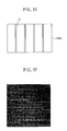
FIG. 1F is a photograph of a polycrystalline silicon layer crystallized in an exemplary embodiment of the present invention; -
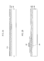
FIGS. 2A through 2C illustrate a thin film transistor according to another exemplary embodiment of the present invention; and -
FIGS. 3A and3B illustrate an OLED display device according to another exemplary embodiment of the present invention. - Reference will now be made in detail to the present embodiments of the present invention, examples of which are illustrated in the accompanying drawings, wherein like reference numerals refer to the like elements throughout. The embodiments are described below in order to explain the present invention by referring to the figures.
- Here, it is to be understood that where it is stated that one film or layer is "formed on" or "disposed on" a second layer or film, the first layer or film may be formed or disposed directly on the second layer or film or there may be intervening layers or films between the first layer or film and the second layer or film. Further, as used herein, the term "formed on" is used with the same meaning as "located on" or "disposed on" and is not meant to be limiting regarding any particular fabrication process. Further, some of the elements that are not essential to the complete understanding of the invention are omitted for clarity.
-
FIGS. 1A through 1E are views according to an exemplary embodiment of the present invention. Referring toFIG. 1A , abuffer layer 110 is formed on asubstrate 100. Thesubstrate 100 can be made of, for example, glass or plastic. Thebuffer layer 110 is formed by chemical vapor deposition (CVD) or physical vapor deposition (PVD) in a single layer or double layer structure using insulating layers, such as a silicon oxide layer and a silicon nitride layer. Thebuffer layer 110 may be formed in a double layer structure of a silicon nitride layer and a silicon oxide layer to facilitate diffusion of a metal catalyst. - Referring to
FIG. 1B , anamorphous silicon layer 120A is formed on thebuffer layer 110 formed on thesubstrate 100. Here, one or more grooves A are formed, for example by scratching a surface of the formedamorphous silicon layer 120A. The grooves A may be formed in a continuous line as shown, but the invention is not limited thereto. A crystal shape may be controlled according to the width and depth of the grooves A. - After forming the grooves A, referring to
FIG. 1C , acapping layer 125 and ametal catalyst layer 128 are sequentially formed on theamorphous silicon layer 120A having the grooves A. As shown, thecapping layer 125 is formed to a thickness of 1 to 200nm (10 to 2000 Å). When the thickness is less than 1nm (10 Å), it is difficult to prevent diffusion of a metal catalyst present in thecapping layer 125 into theamorphous silicon layer 120A, and when the thickness is more than 200nm (2000 Å), it is difficult to crystallize theamorphous silicon layer 120A to be formed later into apolycrystalline silicon layer 120B because of a small amount of the metal catalyst diffused into theamorphous silicon layer 120A. - The
metal catalyst layer 128 may be formed of a material selected from the group consisting of Ni, Pd, Ag, Au, Al, Sn, Sb, Cu, Tr and Cd, and preferably, is made of Ni. Here, themetal catalyst layer 128 is formed on thecapping layer 125 to have an areal density of 1011 to 1015 atoms/cm2. When the areal density of themetal catalyst layer 128 is less than 1011 atoms/cm2, it is difficult to crystallize theamorphous silicon layer 120A into thepolycrystalline silicon layer 120B because an amount of a seed, which is a core of crystallization, is small. When the areal density of themetal catalyst layer 128 is more than 1015 atoms/cm2, a crystal grain of thepolycrystalline silicon layer 120B becomes smaller because of a large amount of the metal catalyst diffused into theamorphous silicon layer 120A, and an amount of a remaining metal catalyst is increased, thereby degrading characteristics of a semiconductor layer formed by patterning thepolycrystalline silicon layer 120B. - After forming the metal catalyst and capping
layers substrate 100 is annealed (H) to crystallize theamorphous silicon layer 120A into apolycrystalline silicon layer 120B ofFIG. 1D using the metal catalyst. Here, the annealing (H) process is performed in the range of 200 to 900 °C for several seconds to hours to diffuse the metal catalyst A, which prevents deformation of thesubstrate 100 due to an excessive annealing process, and is preferable in aspects of production costs and yields. The annealing (H) process may be one of furnace, rapid thermal annealing, UV and laser processes. - Subsequently, referring to
FIG. 1D , the crystallizedpolycrystalline silicon layer 120B was formed by the annealing (H) process, and thecapping layer 125 and themetal catalyst layer 128 are removed from thesubstrate 100. As shown, thepolycrystalline silicon layer 120B includes aseed region 120S under the grooves A. In theseed region 120S, a metal silicide formed by bonding the metal catalyst diffused from themetal catalyst layer 128 to theamorphous silicon layer 120A, as a seed, starts to be crystallized, and the seeds are collected in the grooves A to be disposed in a linear pattern like the grooves A. - It can be seen from
FIG. 1F that the seeds are connected to each other and formed in a linear pattern, and uniform crystals are laterally grown from the seeds. - Thus, the linear-patterned seeds are formed by collecting the seeds in the grooves A formed by scratching. It can be seen that a location where the seed is formed can be controlled by simply scratching a surface of the
amorphous silicon layer 120A, and thus the growth of the crystal may be controlled. Therefore, a semiconductor layer is selectively formed by controlling the seed to control crystallinity of thepolycrystalline silicon layer 120B, so that a thin film transistor (TFT) having the semiconductor layer having an improved uniformity in crystallinity and a device having the same may be fabricated. - While, in the exemplary embodiment, the grooves A are formed in the
amorphous silicon layer 120A and then crystallized, the grooves A may be formed on thebuffer layer 110 or thecapping layer 125 instead of theamorphous silicon layer 120A, thereby performing crystallization in the same manner as described above. -
FIGS. 2A through 2C illustrate a TFT formed by the method of forming apolycrystalline silicon layer 220B described in an exemplary embodiment of the present invention. Hereinafter, since thepolycrystalline silicon layer 220B is formed by the method of forming thepolycrystalline silicon layer 120B described above in relation toFIGS. 1A through 1F , like descriptions will be omitted to avoid repetition. - Referring to
FIG. 2A , crystallization is performed to form thepolycrystalline silicon layer 220B, and a seed (i.e., a metal silicide formed of a metal catalyst and a silicon layer), is formed under grooves A in thepolycrystalline silicon layer 220B, thereby forming aseed region 220S. Theseed region 220S is formed along the linear patterned grooves A. The crystal is laterally grown from the seed. - Referring to
FIG. 2B , the crystallizedpolycrystalline silicon layer 220B is patterned, thereby forming asemiconductor layer 220. Here, since the seed region 220s is formed under the grooves A in thepolycrystalline silicon layer 220B, thesemiconductor layer 220 is patterned such that a groove is not formed in a channel region influencing characteristics of thesemiconductor layer 220, and current flow of thesemiconductor layer 220 becomes perpendicular to the groove A. - After forming the
semiconductor layer 220, agate insulating layer 230 is formed on the entire surface of thesubstrate 200 and covering thesemiconductor layer 220. Thegate insulating layer 230 may be formed of a silicon oxide layer, a silicon nitride layer or a double layer thereof. - Subsequently, a
gate electrode 240 corresponding to thesemiconductor layer 220 is formed on thegate insulating layer 230. Thegate electrode 240 is formed of a metal layer (not shown) in a single layer structure of aluminum (Al) or an Al alloy such as aluminum-neodymium (Al-Nd) or a double layer structure in which an aluminum alloy is stacked on a chromium (Cr) or molybdenum (Mo) alloy through photolithography and etching. - Referring to
FIG. 2C , aninterlayer insulating layer 250 is formed on the entire surface of thesubstrate 200 covering thegate electrode 240 and thegate insulating layer 230. Source anddrain electrodes gate electrode 240 and electrically connected to thesemiconductor layer 220. Thus, the TFT is completed. - Another exemplary embodiment of the present invention relates to an OLED display device having the TFT described in
FIGS. 2A-2C , and thus like descriptions will be omitted to avoid repetition. -
FIGS. 3A and3B illustrate an OLED display device according to another exemplary embodiment of the present invention. Referring toFIG. 3A , an insulatinglayer 270 is formed on the entire surface of thesubstrate 200 and covering the TFT. - A
first electrode 280 is formed on the insulatinglayer 270 and is electrically connected to one of source anddrain electrodes layer 250. - Referring to
FIG. 3B , apixel defining layer 285 exposing a part of thefirst electrode 280 and defining a pixel is formed on the insulatinglayer 270. Anorganic layer 290 having an organic emitting layer is formed on the exposedfirst electrode 280. - After forming the
organic layer 290, asecond electrode 295 is formed on the entire surface of thesubstrate 200 to cover thepixel defining layer 285 and theorganic layer 290, and thus the OLED display device is completed. - In a comparative example, a procedure of forming grooves in an amorphous silicon layer by scratching the amorphous silicon layer as noted in one of the exemplary embodiments of the present invention is omitted, while other procedures are the same as those described in the exemplary embodiments of the present invention. Thus, to avoid repetition, like descriptions will be omitted.
- Table 1 shows data comparing characteristic distributions between the TFT according to an exemplary embodiment of the present invention and a TFT according to the comparative example in which SGS crystallization is performed without formation of grooves.
[Table 1] Distribution (V) of Threshold Voltage (Vth) Distribution of Electron Mobility (cm2/V.sec) Distribution of S Factor Distribution of On-Current (µA/µm) Exemplary Embodiment 0.09 1.03 0.04 0.15 Comparative Example 0.21 7.02 0.06 0.82 - Referring to Table 1, in the exemplary embodiment in which the TFT is fabricated by forming the grooves in an upper portion of the amorphous silicon layer to control a seed through crystallization according to an aspect of the present invention, the threshold voltage was 0.09 V, while in the comparative example, the threshold voltage was 0.21 V. Therefore, it can be seen that because the distribution of the threshold voltage of the TFT according to the exemplary embodiment is smaller, the characteristics of the TFT according to the exemplary embodiment are more uniform. In addition, the distributions of the electron mobility were 1.03 cm2/V•sec for the exemplary embodiment, and 7.02 cm2/V•sec for the comparative example. Accordingly, it can be seen that since the distribution value of the exemplary embodiment is lower, the characteristics of the TFT according to the exemplary embodiment are more uniform. The distribution values of the S factor were 0.04 for the exemplary embodiment, and 0.06 for the comparative example, which indicates that the exemplary embodiment exhibits a better S factor characteristic. In addition, the on-current distribution values were 0.15 µA/µm for the exemplary embodiment, and 0.82 µA/µm for the comparative example, which indicates that the exemplary embodiment exhibits a better on-current characteristic.
- Thus, in the TFT formed according to an aspect of the present invention, a seed and a crystal grain can be controlled during crystallization of an amorphous silicon layer. In other words, because the semiconductor layer is selectively formed according to the crystal grain, the TFT formed according to the exemplary embodiment of the present invention may be improved in uniformity of its characteristics. In formation of a device having a plurality of TFTs, when TFTs having uniform characteristics are provided, a device having improved characteristics such as brightness may be produced.
- In the exemplary embodiments of the present invention, the amorphous silicon layer is scratched to form the linear-patterned grooves and then crystallized, but the aspects of the present invention are not limited thereto. Alternatively, even when the grooves are formed in a buffer or capping layer instead of the amorphous silicon layer, and then the amorphous silicon layer is crystallized, the same result may be obtained as described above.
- In the exemplary embodiments, after the capping layer is formed on the amorphous silicon layer and the metal catalyst layer is formed, the crystallization is performed, but the present invention is not limited thereto. Without the capping layer on the amorphous silicon layer, the metal catalyst layer may be directly formed, and then the crystallization may be performed.
- Moreover, in the exemplary embodiments of the present invention, the TFT and the OLED display device are fabricated in a top-gate structure, but the present invention is not limited thereto. Therefore, they may be fabricated in a bottom-gate structure.
- A buffer layer, an amorphous silicon layer or a capping layer disposed in a lower region of a metal catalyst is scratched before crystallization using the metal catalyst to control formation of a metal silicide and thus control a crystal grain of a polycrystalline silicon layer and reduce an amount of the metal catalyst present in a semiconductor layer, so that a thin film transistor having a semiconductor layer whose characteristics are improved, an OLED display device having the same, and methods of fabricating the same may be provided.
- Although the aspects of the present invention has been described with reference to predetermined exemplary embodiments thereof, it will be understood by those skilled in the art that a variety of modifications and variations may be made to the aspects of the present invention without departing from the scope of the present invention as defined in the appended claims.
Claims (15)
- A method of forming a polycrystalline silicon layer, comprising:providing a substrate (100, 200);forming a buffer layer (110, 210) on the substrate;forming an amorphous silicon layer (120A) on the buffer layer;optionally forming a capping layer (125) on the amorphous silicon layer;forming a metal catalyst layer (128) on the amorphous silicon layer or on the capping layer;forming one or more grooves (A) in the buffer layer, the capping layer or the amorphous silicon layer; andannealing the substrate and crystallizing the amorphous silicon layer into a polycrystalline silicon layer (120B, 220B) having one or more metal silicide seed regions (120S) corresponding to the position of the one or more grooves.
- The method according to claim 1, wherein the one or more grooves are formed in a linear pattern.
- The method according to claim 1 or 2, comprising a plurality of grooves, wherein an interval between the grooves is controlled to control a crystal grain size of the polycrystalline silicon layer.
- The method according to any one of the preceding claims, wherein the metal catalyst layer is formed to have an areal density of 1011 to 1015 atoms/cm2.
- The method according to any one of the preceding claims, wherein the annealing is performed at or between 200 and 900 °C.
- A thin film transistor TFT, comprising:a substrate (200);a buffer layer (210) disposed on the substrate;a semiconductor layer (220) disposed on the buffer layer;a gate insulating layer (230) disposed on the entire surface of the semiconductor layer (220);a gate electrode (240) corresponding to the semiconductor layer; andsource and drain electrodes (260a, 260b) insulated from the gate electrode and connected to the semiconductor layer,wherein metal silicide seed regions are disposed in the semiconductor layer corresponding to the location of one or more grooves in the buffer layer or the semiconductor layer.
- The TFT according to claim 6, wherein the one or more grooves are formed in a linear pattern.
- The TFT according to claim 6 or 7, wherein the metal silicide seed regions are continuously disposed along the one or more grooves.
- The TFT according to claim 6, 7, or 8 wherein the one or more grooves are disposed in regions of the semiconductor layer other than a channel region.
- The TFT according to any one of claims 6 to 9, wherein the metal silicide is formed of a material selected from the group consisting of Ni, Pd, Ag, Au, Al, Sn, Sb, Cu, Tr and Cd.
- The TFT according to any one of claims 6 to 10, wherein the one or more grooves are formed perpendicular to a current flow in the semiconductor layer.
- A method of fabricating a thin film transistor TFT, comprising:performing a method according to any one of claims 1 to 5;removing the metal catalyst layer and the optional capping layer;patterning the polycrystalline silicon layer and forming a semiconductor layer (220);forming a gate insulating layer (230) on an entire surface of the semiconductor layer;forming a gate electrode (240) on the gate insulating layer on a portion corresponding to the semiconductor layer; andforming source and drain electrodes (260a, 260b) insulated from the gate electrode and connected to the semiconductor layer.
- The method according to claim 12, wherein the metal catalyst layer is formed of a material selected from the group consisting of Ni, Pd, Ag, Au, Al, Sn, Sb, Cu, Tr and Cd.
- An organic light emitting diode (OLED) display device, comprising:a TFT according to any one of claims 6 to 11;an insulating layer (270) disposed on the entire surface of the substrate; anda first electrode (280) electrically connected to one of the source and drain electrodes;an organic layer (290); anda second electrode (295).
- A method of fabricating an OLED display device, comprising:performing a method according to claim 12 or 13; andforming a first electrode (280) connected to one of the source and drain electrodes, an organic layer (290) and a second electrode (295).
Applications Claiming Priority (1)
| Application Number | Priority Date | Filing Date | Title |
|---|---|---|---|
| KR1020090109835A KR101094295B1 (en) | 2009-11-13 | 2009-11-13 | Manufacturing method of polycrystalline silicon layer, manufacturing method of thin film transistor, and manufacturing method of organic light emitting display device |
Publications (1)
| Publication Number | Publication Date |
|---|---|
| EP2323159A1 true EP2323159A1 (en) | 2011-05-18 |
Family
ID=43479223
Family Applications (1)
| Application Number | Title | Priority Date | Filing Date |
|---|---|---|---|
| EP10191250A Ceased EP2323159A1 (en) | 2009-11-13 | 2010-11-15 | Method of forming polycrystalline silicon layer, thin film transistor, organic light emitting diode display device having the same, and methods of fabricating the same |
Country Status (5)
| Country | Link |
|---|---|
| US (1) | US8890165B2 (en) |
| EP (1) | EP2323159A1 (en) |
| JP (1) | JP6081689B2 (en) |
| KR (1) | KR101094295B1 (en) |
| CN (1) | CN102064089B (en) |
Families Citing this family (7)
| Publication number | Priority date | Publication date | Assignee | Title |
|---|---|---|---|---|
| CN102646595A (en) | 2011-11-11 | 2012-08-22 | 京东方科技集团股份有限公司 | Thin film transistor, manufacturing method and display device thereof |
| US9087694B2 (en) * | 2012-06-03 | 2015-07-21 | Silicon Solar Solutions, Llc | Ultra-large grain polycrystalline semiconductors through top-down aluminum induced crystallization (TAIC) |
| CN103219228B (en) * | 2013-03-11 | 2016-05-25 | 京东方科技集团股份有限公司 | The preparation method of polysilicon layer and polycrystalline SiTFT and manufacture method thereof |
| TWI593024B (en) * | 2015-07-24 | 2017-07-21 | 友達光電股份有限公司 | Method for manufacturing thin film transistor |
| CN106935657B (en) * | 2017-05-04 | 2020-06-02 | 京东方科技集团股份有限公司 | Thin film transistor, manufacturing method thereof and display device |
| CN107946173B (en) * | 2017-10-12 | 2019-12-27 | 惠科股份有限公司 | Method for manufacturing low-temperature polycrystalline silicon thin film and transistor |
| CN114050160B (en) * | 2021-11-09 | 2026-04-21 | 长江存储科技有限责任公司 | Semiconductor device fabrication methods and semiconductor devices |
Citations (8)
| Publication number | Priority date | Publication date | Assignee | Title |
|---|---|---|---|---|
| US6294815B1 (en) * | 1997-08-26 | 2001-09-25 | Semiconductor Energy Laboratory Co., Ltd. | Semiconductor device |
| US20040173796A1 (en) * | 2003-02-07 | 2004-09-09 | Seiko Epson Corporation | Complementary thin film transistor circuit, electro-optical device, and electronic apparatus |
| US20050023531A1 (en) * | 2003-07-31 | 2005-02-03 | Semiconductor Energy Laboratory Co., Ltd. | Semiconductor device and method for manufacturing semiconductor device |
| US20050161742A1 (en) * | 2001-12-28 | 2005-07-28 | Semiconductor Energy Laboratory Co., Ltd. | Semiconductor device and semiconductor device production system |
| US20050275019A1 (en) * | 2004-06-09 | 2005-12-15 | Jin-Wook Seo | Thin film transistor and method of fabricating the same |
| US20060121651A1 (en) * | 2004-07-07 | 2006-06-08 | Byoung-Keon Park | Thin film transistor and method of fabricating the same |
| EP1903604A2 (en) * | 2006-09-19 | 2008-03-26 | Samsung Electronics Co., Ltd. | Organic electro-luminescent display and method of frabricating the same |
| EP2226833A1 (en) * | 2009-03-03 | 2010-09-08 | Samsung Mobile Display Co., Ltd. | Thin film transistor, method of fabricating the same, and organic light emitting diode display device including the same |
Family Cites Families (78)
| Publication number | Priority date | Publication date | Assignee | Title |
|---|---|---|---|---|
| JPS6333868A (en) | 1986-07-28 | 1988-02-13 | Nec Corp | Manufacture of mis field-effect transistor |
| JPS63304668A (en) | 1987-06-03 | 1988-12-12 | Fujitsu Ltd | Manufacture of insulated-gate transistor |
| JP2617950B2 (en) | 1987-10-16 | 1997-06-11 | 松下電器産業株式会社 | Manufacturing method of liquid crystal display device |
| JPH04135161A (en) | 1990-09-21 | 1992-05-08 | Ietatsu Ono | Polishing method and device thereof |
| JP3076119B2 (en) | 1991-12-25 | 2000-08-14 | 株式会社日立製作所 | Manufacturing method of liquid crystal display device |
| EP0589049B1 (en) | 1992-03-25 | 2000-01-12 | Kanegafuchi Chemical Industry Co., Ltd. | Thin polysilicon film and production thereof |
| JP3139154B2 (en) | 1992-08-19 | 2001-02-26 | セイコーエプソン株式会社 | Liquid crystal device and method of manufacturing the same |
| JPH0669515A (en) | 1992-08-19 | 1994-03-11 | Fujitsu Ltd | Semiconductor memory device |
| JP3107941B2 (en) | 1993-03-05 | 2000-11-13 | 株式会社半導体エネルギー研究所 | Thin film transistor and manufacturing method thereof |
| JPH0713196A (en) | 1993-06-21 | 1995-01-17 | Toshiba Corp | Active matrix liquid crystal display |
| KR100294026B1 (en) | 1993-06-24 | 2001-09-17 | 야마자끼 순페이 | Electro-optical device |
| US7081938B1 (en) | 1993-12-03 | 2006-07-25 | Semiconductor Energy Laboratory Co., Ltd. | Electro-optical device and method for manufacturing the same |
| JPH0845850A (en) | 1994-07-27 | 1996-02-16 | Oki Electric Ind Co Ltd | Growth method of doped polycrystalline semiconductor thin film |
| JP3295679B2 (en) | 1995-08-04 | 2002-06-24 | 株式会社半導体エネルギー研究所 | Method for manufacturing semiconductor device |
| JP3143591B2 (en) | 1995-09-14 | 2001-03-07 | キヤノン株式会社 | Display device |
| JP3476320B2 (en) * | 1996-02-23 | 2003-12-10 | 株式会社半導体エネルギー研究所 | Semiconductor thin film and method for manufacturing the same, semiconductor device and method for manufacturing the same |
| TW317643B (en) | 1996-02-23 | 1997-10-11 | Handotai Energy Kenkyusho Kk | |
| KR100205523B1 (en) | 1996-04-08 | 1999-07-01 | 구자홍 | Thin film transistor and its fabrication method |
| JPH1174536A (en) | 1997-01-09 | 1999-03-16 | Sanyo Electric Co Ltd | Method for manufacturing semiconductor device |
| KR20000055877A (en) | 1999-02-10 | 2000-09-15 | 장진 | Polycrystalline silicon containing nickel |
| KR100317638B1 (en) | 1999-03-19 | 2001-12-22 | 구본준, 론 위라하디락사 | Polysilicon-thin film transister device and A method of fabricating the same |
| US6878968B1 (en) | 1999-05-10 | 2005-04-12 | Semiconductor Energy Laboratory Co., Ltd. | Semiconductor device |
| JP3706527B2 (en) | 1999-06-30 | 2005-10-12 | Hoya株式会社 | Electron beam drawing mask blanks, electron beam drawing mask, and method of manufacturing electron beam drawing mask |
| JP3715848B2 (en) | 1999-09-22 | 2005-11-16 | シャープ株式会社 | Manufacturing method of semiconductor device |
| US6294442B1 (en) | 1999-12-10 | 2001-09-25 | National Semiconductor Corporation | Method for the formation of a polysilicon layer with a controlled, small silicon grain size during semiconductor device fabrication |
| JP4200618B2 (en) | 1999-12-27 | 2008-12-24 | ソニー株式会社 | Semiconductor film forming method and thin film semiconductor device manufacturing method |
| GB2358081B (en) | 2000-01-07 | 2004-02-18 | Seiko Epson Corp | A thin-film transistor and a method for maufacturing thereof |
| KR100450595B1 (en) | 2000-02-09 | 2004-09-30 | 히다찌 케이블 리미티드 | Crystalline silicon semiconductor device and method for fabricating same |
| JP4769997B2 (en) | 2000-04-06 | 2011-09-07 | ソニー株式会社 | THIN FILM TRANSISTOR AND ITS MANUFACTURING METHOD, LIQUID CRYSTAL DISPLAY DEVICE, LIQUID CRYSTAL DISPLAY DEVICE MANUFACTURING METHOD, ORGANIC EL DEVICE, AND ORGANIC EL DEVICE MANUFACTURING METHOD |
| JP2001337348A (en) | 2000-05-30 | 2001-12-07 | Toshiba Corp | Array substrate and method of manufacturing the same |
| KR100387122B1 (en) | 2000-09-15 | 2003-06-12 | 피티플러스(주) | Fabrication Method of Poly-Si Thin Film Transistor Having Back Bias Effects |
| JP4267266B2 (en) | 2001-07-10 | 2009-05-27 | 株式会社半導体エネルギー研究所 | Method for manufacturing semiconductor device |
| JP2003060209A (en) | 2001-08-08 | 2003-02-28 | Sharp Corp | Semiconductor device and method of manufacturing the same |
| JP2003100629A (en) | 2001-09-19 | 2003-04-04 | Sharp Corp | Semiconductor device and manufacturing method thereof |
| JP4135347B2 (en) | 2001-10-02 | 2008-08-20 | 株式会社日立製作所 | Method for producing polysilicon film |
| JP2003188098A (en) | 2001-12-13 | 2003-07-04 | Sharp Corp | Semiconductor device and method of manufacturing the same |
| TW536716B (en) | 2002-07-04 | 2003-06-11 | Ind Tech Res Inst | Capacitor structure of low temperature polysilicon |
| JP4092261B2 (en) * | 2002-08-02 | 2008-05-28 | 三星エスディアイ株式会社 | Manufacturing method of substrate and manufacturing method of organic electroluminescence element |
| KR100603284B1 (en) | 2002-10-22 | 2006-07-20 | 삼성에스디아이 주식회사 | Electroluminescent Display Panels with Increased Capacitance |
| KR20040036761A (en) | 2002-10-24 | 2004-05-03 | 엘지전자 주식회사 | Method of silicon deposition using of hdp-cvd |
| KR100470274B1 (en) | 2002-11-08 | 2005-02-05 | 진 장 | Method of phase transition of amorphous material using a cap layer |
| JP4115252B2 (en) | 2002-11-08 | 2008-07-09 | シャープ株式会社 | Semiconductor film and manufacturing method thereof, and semiconductor device and manufacturing method thereof |
| TWI305681B (en) | 2002-11-22 | 2009-01-21 | Toppoly Optoelectronics Corp | Method for fabricating thin film transistor array and driving circuits |
| JP3904512B2 (en) | 2002-12-24 | 2007-04-11 | シャープ株式会社 | SEMICONDUCTOR DEVICE, ITS MANUFACTURING METHOD, AND ELECTRONIC DEVICE PROVIDED WITH SEMICONDUCTOR DEVICE |
| TW200520229A (en) | 2003-12-03 | 2005-06-16 | Toppoly Optoelectronics Corp | Thin film transistor of multi-gate structure and its manufacturing method |
| US7238963B2 (en) | 2003-04-28 | 2007-07-03 | Tpo Displays Corp. | Self-aligned LDD thin-film transistor and method of fabricating the same |
| KR20040098958A (en) | 2003-05-16 | 2004-11-26 | 삼성에스디아이 주식회사 | Thin film transistor and method for fabricating the same |
| JP4578877B2 (en) | 2003-07-31 | 2010-11-10 | 株式会社半導体エネルギー研究所 | Semiconductor device and manufacturing method thereof |
| KR100623228B1 (en) | 2003-11-27 | 2006-09-18 | 삼성에스디아이 주식회사 | A thin film transistor, an organic light emitting display device having the thin film transistor, and a manufacturing method of the thin film transistor |
| KR100579188B1 (en) | 2004-02-12 | 2006-05-11 | 삼성에스디아이 주식회사 | Thin Film Transistor with LED Structure |
| US8114719B2 (en) | 2004-06-03 | 2012-02-14 | Semiconductor Energy Laboratory Co., Ltd. | Memory device and manufacturing method of the same |
| KR100626007B1 (en) | 2004-06-30 | 2006-09-20 | 삼성에스디아이 주식회사 | A thin film transistor, a method of manufacturing the thin film transistor, a flat panel display device having a thin film transistor, and a method of manufacturing a flat panel display device |
| KR100611764B1 (en) | 2004-08-20 | 2006-08-10 | 삼성에스디아이 주식회사 | Manufacturing Method of Thin Film Transistor |
| KR100611766B1 (en) | 2004-08-24 | 2006-08-10 | 삼성에스디아이 주식회사 | Method of manufacturing thin film transistor |
| US7416928B2 (en) | 2004-09-08 | 2008-08-26 | Semiconductor Energy Laboratory Co., Ltd. | Manufacturing method of semiconductor device |
| KR100628989B1 (en) | 2004-09-17 | 2006-09-27 | 진 장 | Crystallization Method of Amorphous Silicon Thin Film |
| KR20060026776A (en) | 2004-09-21 | 2006-03-24 | 삼성에스디아이 주식회사 | Organic electroluminescent device and manufacturing method thereof |
| KR100689316B1 (en) | 2004-10-29 | 2007-03-08 | 엘지.필립스 엘시디 주식회사 | Organic light emitting diode device and manufacturing method thereof |
| KR100669789B1 (en) | 2004-11-26 | 2007-01-16 | 삼성에스디아이 주식회사 | Flat panel display device |
| JP5073482B2 (en) | 2005-03-31 | 2012-11-14 | 東京エレクトロン株式会社 | Silicon oxide film manufacturing method, control program thereof, storage medium, and plasma processing apparatus |
| US7341907B2 (en) | 2005-04-05 | 2008-03-11 | Applied Materials, Inc. | Single wafer thermal CVD processes for hemispherical grained silicon and nano-crystalline grain-sized polysilicon |
| US7652291B2 (en) | 2005-05-28 | 2010-01-26 | Samsung Mobile Display Co., Ltd. | Flat panel display |
| TWI401802B (en) | 2005-06-30 | 2013-07-11 | 三星電子股份有限公司 | Thin film transistor plate and method of manufacturing same |
| JP2007027202A (en) | 2005-07-12 | 2007-02-01 | Sharp Corp | Display device manufacturing method and display device |
| JP2007035812A (en) | 2005-07-26 | 2007-02-08 | Mitsubishi Electric Corp | Polycrystalline silicon film manufacturing method and thin film transistor |
| KR100778781B1 (en) | 2005-12-16 | 2007-11-27 | 주식회사 테라세미콘 | Polycrystalline silicon thin film manufacturing method and apparatus for manufacturing same |
| JP4815600B2 (en) | 2005-09-06 | 2011-11-16 | 株式会社テラセミコン | Polycrystalline silicon thin film manufacturing method and manufacturing apparatus thereof |
| US20080258186A1 (en) | 2005-12-19 | 2008-10-23 | Nxp B.V. | Source and Drain Formation in Silicon on Insulator Device |
| KR20070076860A (en) | 2006-01-20 | 2007-07-25 | 삼성전자주식회사 | Organic light emitting display and manufacturing method |
| TWI296855B (en) | 2006-03-07 | 2008-05-11 | Au Optronics Corp | Thin film transistor and manufacturing method thereof |
| KR100770269B1 (en) | 2006-05-18 | 2007-10-25 | 삼성에스디아이 주식회사 | Method of manufacturing thin film transistor |
| KR100770266B1 (en) | 2006-11-10 | 2007-10-25 | 삼성에스디아이 주식회사 | Organic light emitting display device and manufacturing method |
| KR100864884B1 (en) | 2006-12-28 | 2008-10-22 | 삼성에스디아이 주식회사 | Thin film transistor, manufacturing method thereof and organic light emitting display device having same |
| KR100864883B1 (en) | 2006-12-28 | 2008-10-22 | 삼성에스디아이 주식회사 | A thin film transistor, a manufacturing method thereof, and an organic light emitting display device having the same. |
| KR100839735B1 (en) | 2006-12-29 | 2008-06-19 | 삼성에스디아이 주식회사 | Transistor, manufacturing method thereof and flat panel display device having same |
| KR100889626B1 (en) | 2007-08-22 | 2009-03-20 | 삼성모바일디스플레이주식회사 | Thin film transistor, manufacturing method thereof, organic light emitting display device having same, and manufacturing method thereof |
| JP2009059940A (en) | 2007-08-31 | 2009-03-19 | Sharp Corp | THIN FILM TRANSISTOR, METHOD FOR MANUFACTURING THIN FILM TRANSISTOR, AND ELECTRONIC DEVICE |
| KR20080086967A (en) | 2008-08-28 | 2008-09-29 | 삼성에스디아이 주식회사 | Thin film transistor and organic light emitting display device having same |
-
2009
- 2009-11-13 KR KR1020090109835A patent/KR101094295B1/en not_active Expired - Fee Related
-
2010
- 2010-02-26 US US12/714,154 patent/US8890165B2/en not_active Expired - Fee Related
- 2010-10-12 CN CN201010506428.5A patent/CN102064089B/en not_active Expired - Fee Related
- 2010-10-13 JP JP2010230428A patent/JP6081689B2/en not_active Expired - Fee Related
- 2010-11-15 EP EP10191250A patent/EP2323159A1/en not_active Ceased
Patent Citations (8)
| Publication number | Priority date | Publication date | Assignee | Title |
|---|---|---|---|---|
| US6294815B1 (en) * | 1997-08-26 | 2001-09-25 | Semiconductor Energy Laboratory Co., Ltd. | Semiconductor device |
| US20050161742A1 (en) * | 2001-12-28 | 2005-07-28 | Semiconductor Energy Laboratory Co., Ltd. | Semiconductor device and semiconductor device production system |
| US20040173796A1 (en) * | 2003-02-07 | 2004-09-09 | Seiko Epson Corporation | Complementary thin film transistor circuit, electro-optical device, and electronic apparatus |
| US20050023531A1 (en) * | 2003-07-31 | 2005-02-03 | Semiconductor Energy Laboratory Co., Ltd. | Semiconductor device and method for manufacturing semiconductor device |
| US20050275019A1 (en) * | 2004-06-09 | 2005-12-15 | Jin-Wook Seo | Thin film transistor and method of fabricating the same |
| US20060121651A1 (en) * | 2004-07-07 | 2006-06-08 | Byoung-Keon Park | Thin film transistor and method of fabricating the same |
| EP1903604A2 (en) * | 2006-09-19 | 2008-03-26 | Samsung Electronics Co., Ltd. | Organic electro-luminescent display and method of frabricating the same |
| EP2226833A1 (en) * | 2009-03-03 | 2010-09-08 | Samsung Mobile Display Co., Ltd. | Thin film transistor, method of fabricating the same, and organic light emitting diode display device including the same |
Also Published As
| Publication number | Publication date |
|---|---|
| KR20110053039A (en) | 2011-05-19 |
| KR101094295B1 (en) | 2011-12-19 |
| US8890165B2 (en) | 2014-11-18 |
| US20110114961A1 (en) | 2011-05-19 |
| JP6081689B2 (en) | 2017-02-15 |
| JP2011109075A (en) | 2011-06-02 |
| CN102064089A (en) | 2011-05-18 |
| CN102064089B (en) | 2016-03-02 |
Similar Documents
| Publication | Publication Date | Title |
|---|---|---|
| US8790967B2 (en) | Method of fabricating polycrystalline silicon layer, TFT fabricated using the same, method of fabricating TFT, and organic light emitting diode display device having the same | |
| US9035311B2 (en) | Organic light emitting diode display device and method of fabricating the same | |
| US9576797B2 (en) | Method of fabricating polysilicon layer, thin film transistor, organic light emitting diode display device including the same, and method of fabricating the same | |
| US8384087B2 (en) | Thin film transistor, organic light emitting diode display device having the same, and method of fabricating the same | |
| JP2008166785A (en) | Thin film transistor, manufacturing method thereof, and organic light emitting display | |
| US20060030085A1 (en) | Method of fabricating thin film transistor | |
| EP2323159A1 (en) | Method of forming polycrystalline silicon layer, thin film transistor, organic light emitting diode display device having the same, and methods of fabricating the same | |
| EP2204844A1 (en) | Method of fabricating polysilicon, thin film transistor, method of fabricating the thin film transistor, and organic light emitting diode display device including the thin film transistor | |
| US20070284581A1 (en) | Method of fabricating pmos thin film transistor | |
| EP2226848A1 (en) | Thin film transistor, method of fabricating the same, and organic light emitting diode display device having the same | |
| US8294158B2 (en) | Thin film transistor, method of fabricating the same, and organic light emitting diode display device including the thin film transistor | |
| US8125033B2 (en) | Polycrystalline silicon layer, flat panel display using the same, and method of fabricating the same | |
| JP5274341B2 (en) | THIN FILM TRANSISTOR, MANUFACTURING METHOD THEREOF, AND ORGANIC ELECTROLUMINESCENT DISPLAY DEVICE INCLUDING THE SAME |
Legal Events
| Date | Code | Title | Description |
|---|---|---|---|
| PUAI | Public reference made under article 153(3) epc to a published international application that has entered the european phase |
Free format text: ORIGINAL CODE: 0009012 |
|
| AK | Designated contracting states |
Kind code of ref document: A1 Designated state(s): AL AT BE BG CH CY CZ DE DK EE ES FI FR GB GR HR HU IE IS IT LI LT LU LV MC MK MT NL NO PL PT RO RS SE SI SK SM TR |
|
| AX | Request for extension of the european patent |
Extension state: BA ME |
|
| 17P | Request for examination filed |
Effective date: 20110630 |
|
| RAP1 | Party data changed (applicant data changed or rights of an application transferred) |
Owner name: SAMSUNG DISPLAY CO., LTD. |
|
| RAP1 | Party data changed (applicant data changed or rights of an application transferred) |
Owner name: SAMSUNG DISPLAY CO., LTD. |
|
| STAA | Information on the status of an ep patent application or granted ep patent |
Free format text: STATUS: EXAMINATION IS IN PROGRESS |
|
| 17Q | First examination report despatched |
Effective date: 20170103 |
|
| STAA | Information on the status of an ep patent application or granted ep patent |
Free format text: STATUS: THE APPLICATION HAS BEEN REFUSED |
|
| 18R | Application refused |
Effective date: 20180116 |