EP2320192A1 - Photoelectric Sensor - Google Patents
Photoelectric Sensor Download PDFInfo
- Publication number
- EP2320192A1 EP2320192A1 EP10189644A EP10189644A EP2320192A1 EP 2320192 A1 EP2320192 A1 EP 2320192A1 EP 10189644 A EP10189644 A EP 10189644A EP 10189644 A EP10189644 A EP 10189644A EP 2320192 A1 EP2320192 A1 EP 2320192A1
- Authority
- EP
- European Patent Office
- Prior art keywords
- light
- phototransmitter
- optical filters
- optical
- kinds
- Prior art date
- Legal status (The legal status is an assumption and is not a legal conclusion. Google has not performed a legal analysis and makes no representation as to the accuracy of the status listed.)
- Granted
Links
- 230000003287 optical effect Effects 0.000 claims abstract description 171
- 238000001514 detection method Methods 0.000 claims abstract description 107
- 239000000758 substrate Substances 0.000 description 30
- 239000013307 optical fiber Substances 0.000 description 12
- 230000005540 biological transmission Effects 0.000 description 10
- 239000000835 fiber Substances 0.000 description 7
- 238000000034 method Methods 0.000 description 5
- 235000012431 wafers Nutrition 0.000 description 3
- 230000015556 catabolic process Effects 0.000 description 1
- 239000011248 coating agent Substances 0.000 description 1
- 238000000576 coating method Methods 0.000 description 1
- 238000006731 degradation reaction Methods 0.000 description 1
- 230000002708 enhancing effect Effects 0.000 description 1
- 230000001939 inductive effect Effects 0.000 description 1
- 239000000463 material Substances 0.000 description 1
- 230000010287 polarization Effects 0.000 description 1
- 230000035945 sensitivity Effects 0.000 description 1
Images


Classifications
-
- G—PHYSICS
- G01—MEASURING; TESTING
- G01B—MEASURING LENGTH, THICKNESS OR SIMILAR LINEAR DIMENSIONS; MEASURING ANGLES; MEASURING AREAS; MEASURING IRREGULARITIES OF SURFACES OR CONTOURS
- G01B11/00—Measuring arrangements characterised by the use of optical techniques
-
- G—PHYSICS
- G01—MEASURING; TESTING
- G01B—MEASURING LENGTH, THICKNESS OR SIMILAR LINEAR DIMENSIONS; MEASURING ANGLES; MEASURING AREAS; MEASURING IRREGULARITIES OF SURFACES OR CONTOURS
- G01B11/00—Measuring arrangements characterised by the use of optical techniques
- G01B11/02—Measuring arrangements characterised by the use of optical techniques for measuring length, width or thickness
-
- G—PHYSICS
- G01—MEASURING; TESTING
- G01V—GEOPHYSICS; GRAVITATIONAL MEASUREMENTS; DETECTING MASSES OR OBJECTS; TAGS
- G01V8/00—Prospecting or detecting by optical means
- G01V8/10—Detecting, e.g. by using light barriers
- G01V8/12—Detecting, e.g. by using light barriers using one transmitter and one receiver
Abstract
Description
- The present invention relates to a photoelectric sensor used to detect an object, particularly to a photoelectric sensor suitable for use of detection of a thin object.
- In a photoelectric sensor that is used to detect a thickness portion of a thin object in a substrate conveying line or the like, since a complete light interception state is hardly generated depending on a detection target object, a detection signal is turned on based on a condition that an amount of received light is lower than a predetermined threshold.
- In a conventional example concerning a disposition of this kind of sensor, as shown in
Fig. 10 , a phototransmitter 501 and anoptical receiver 502 of a transmission type photoelectric sensor are disposed such that a detection target region is sandwiched therebetween, and a decrease of the amount of received light is detected when light traveling from the phototransmitter 501 toward theoptical receiver 502 is partially intercepted by a substrate 503 (for examples, see Japanese Unexamined Patent Publication No.2009-216489 Fig. 11 , the phototransmitter 501 and theoptical receiver 502 are disposed while vertically deviated from each other, and the phototransmitter outputs the light such that the light obliquely traverses the detection target region (for example, see Japanese Unexamined Patent Publication No.2007-258386 - In Japanese Unexamined Patent Publication Nos.
2009-216489 2007- 258386 6-69323 - In the example of
Fig. 10 , since a light interception amount depends on a thickness of thesubstrate 503, the detection is hardly performed when thesubstrate 503 is thinned. As shown inFig. 12 , depending on the disposition of the sensor, the light outputted from the phototransmitter 501 is reflected by a surface of thesubstrate 503 and is incident to theoptical receiver 502. Therefore, occasionally the detection of thesubstrate 503 is obstructed. - When the optical path is set in the oblique direction like the example of
Fig. 11 , since a light interception state is generated by the surface of thesubstrate 503, it seems that the light interception amount can be increased to stably perform the detection. However, in the above disposition, the phototransmitter 501 differs from theoptical receiver 502 in height, so that it is difficult to align thesubstrate 503 and the optical path with each other. In order to stably detect thesubstrate 503 in horizontal behavior, as shown in a region 500 ofFig. 11 , it is necessary that a detection region having a width in which the substrate can be included be produced in a certain degree of height range. However, when the optical path is set obliquely, undetectable regions u and v are generated in the region 500 that should be the detection region. - In order to eliminate the undetectable regions u and v, another set of the phototransmitter and the optical receiver is disposed near the phototransmitter 501 and the
optical receiver 502 with a positional relationship opposite to that ofFig. 11 . However, in such a configuration, wiring becomes complicated to increase cost. Possibly the reflected light generated in the optical path of one of the sensors is incident to the optical receiver of the other sensor to degrade detection accuracy. - The present invention has been devised to solve the problems described above, and an object thereof is to be able to stably detect a thin target object.
- In accordance with one aspect of the present invention, the invention is applied to a photoelectric sensor including: a phototransmitter that outputs light toward a detection target region of an object; and an optical receiver that receives the light outputted from the phototransmitter, wherein a signal indicating that the object is detected is outputted in response to a decrease of an amount of light received by the optical receiver. The photoelectric sensor can be configured not only as a sensor in which the phototransmitter and the optical receiver respectively contain a light source and a light receiving element, but also as an optical fiber type photoelectric sensor. Moreover, the present invention can be applied to a transmission type photoelectric sensor as well as a reflection type photoelectric sensor.
- In the phototransmitter of the photoelectric sensor according to the present invention, two kinds of light having different characteristics and that do not interfere with each other are outputted from two output regions into which the light transmitting surface is divided. In addition, the photoelectric sensor according to the present invention includes a pair of optical filters having a characteristic of selecting the two kinds of light and guiding the light to the optical receiver. The optical filters are disposed opposite to output regions of the pieces of light different from the pieces of light of a selecting target while located across a detection target region. Moreover, output directions of the two kinds of light are fixed such that whole surfaces of the first optical filters corresponding to the characteristics are irradiated with the two kinds of light from the phototransmitter when the first optical filters are disposed in a light transmitting surface while located away from each other by a predetermined distance or more.
- According to the above configuration, when the optical filters are disposed while located away from the light transmitting surface by a predetermined distance or more, the two kinds of light outputted from the phototransmitter travel in the detection target region, the whole surface of the optical filters corresponding to the characteristics of the two kinds of light are irradiated with the two kinds of light, and the two kinds of light are incident to the optical receiver through the optical filters. The range, in which the light incident to the optical receiver travels, acts as the object detection region.
- The detection regions by the two kinds of light obliquely traverse the detection target region and intersect each other in the detection target region. The detection regions intersect each other with the widths corresponding to the output regions of the pieces of corresponding light or the optical filters in the range from a boundary position between the output regions of the light transmitting surface to a boundary position between the optical filters, so that the detection regions can be distributed in the wide range centering around the intersection portion.
- In the position that is opposite to the output region of each piece of light in the phototransmitter, the optical filter corresponding to the light whose characteristic differs from that of the light outputted from the region is disposed. Therefore, even if the light reflected from the surface of the object is guided to the optical receiver, the incidence of the reflected light to the optical receiver can be prevented.
- In the photoelectric sensor according to a preferred aspect, an optical axis setting unit is provided in the phototransmitter, and the optical axis setting unit changes an optical axis direction of the light from a light source to the output regions of the two kinds of light to a direction in which the optical filters are disposed such that the light obliquely traverses the detection target region toward the positions in which the optical filters are disposed. With such a configuration, even if the distance between the light transmitting surface and the optical filter is not lengthened, the whole surfaces of the corresponding optical filters can be irradiated with the two kinds of light to increase a degree of freedom of the distance set between the light transmitting surface and the optical filter. Therefore, the photoelectric sensor can deal with the detection of the objects having various widths.
- In the photoelectric sensor according to the preferred aspect, the pair of first optical filters is integrally provided in the optical receiver while arrayed in parallel in a light receiving surface of the optical receiver. The optical receiver is disposed opposite to the phototransmitter along with the optical filters to receive the pieces of light passing through the optical filters. Therefore, the sensor in which the detection accuracy is largely improved can be provided as the transmission type photoelectric sensor.
- Further, in the above aspect, the optical receiver is configured to individually collect the pieces of light passing through the optical filters and individually guide the pieces of collected light to light receiving elements. With such a configuration, the object is detected based on the decrease of the amount of received light in one of the light receiving elements, so that the stable detection can be performed even if the object of the detection target is biased to one of the detection regions by the two kinds of light.
- In another preferred aspect, the phototransmitter and the optical receiver are provided in the same housing on an assumption that a return reflector plate is provided on an opposite side to the detection target region with respect to the pair of optical filters; and in the housing, a surface that is opposite to the detection target region acts as a light transmitting surface and a light receiving surface. In the pieces of light outputted from the light transmitting unit to pass through the optical filters, the optical receiver receives the pieces of light that are returned through the optical filters after being reflected by the return reflector plate.
- According to the above aspect, the sensor that can stably perform the detection in the wide range can be provided as the reflection type photoelectric sensor.
- In yet another preferred aspect, two kinds of light vibrated in specific directions and having different vibration directions are outputted from a light transmitting surface of the phototransmitter. Moreover, a pair of polarizing plates is disposed as the pair of optical filters opposite to the output regions of the pieces of light that are not the selection target while located across a detection target region, the pair of polarizing plates being directed to the selection of the vibration directions of the two kinds of light.
According to this aspect, the detection can stably be performed by utilizing the characteristic of the light that is vibrated in a specific direction. - According to still another preferred aspect, two kinds of light having different wavelength ranges are outputted from a light transmitting surface of the phototransmitter. The pair of optical filters is directed to the selection of the wavelength ranges corresponding to the two kinds of light; and the pair of optical filters is disposed opposite to the output regions of the pieces of light that are not the selection target while located across a detection target region.
According to this aspect, the detection can stably be performed by utilizing the characteristics of the pieces of light having the different wavelength ranges. - In the phototransmitter according a preferred aspect, a pair of optical filters inducing characteristics identical to those of the pair of optical filters is arrayed along the light transmitting surface so as to be opposite to the optical filters having different characteristics, the optical filters being located across the detection target region; and the pieces of the light passing through the first optical filters of the phototransmitter are outputted as the two kinds of light. In this manner, by using the two pairs of optical filters having different characteristics, the two kinds of light are stably outputted from the phototransmitter, and the light that obliquely traverses the detection target region to reach the position where the optical filter corresponding to the characteristic of the light is disposed can be guided to the optical receiver.
- In the present invention, the two kinds of light having different characteristics are outputted from two regions into which the light transmitting surface is divided, and the two kinds of light does not interfere with each other. The detection regions by the two kinds of light obliquely traverse the detection target region and intersect each other in the detection target region, so that the object can be detected in the wide range of the detection target region.
- The light reflected from the output region is obstructed by the optical filter disposed opposite to the output region of each piece of light of the phototransmitter in the detection target region, so that the degradation of detection accuracy caused by the light reflected from the surface of the detection target can be prevented.
- Accordingly, in the present invention, the detection can stably be performed irrespective of the variations of the width and position of the thin detection target object or the influence of the light reflected from the detection target object.
-
-
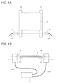
Figs. 1A and 1B show a usage example of a transmission type photoelectric sensor; -
Fig. 2 shows a configuration example and a detection principle of an optical system of the transmission type photoelectric sensor; -
Figs. 3A and 3B each show a relationship between broadening ranges of pieces of light from a phototransmitter and pieces of light incident to an optical receiver; -
Figs. 4A and 4B each show a relationship between the broadening ranges of the pieces of light from the phototransmitter and the pieces of light incident to the optical receiver when an optical axis is not adjusted by a prism; -
Fig. 5 shows another configuration example and a detection principle of the optical system; -
Fig. 6 shows still another configuration example and a detection principle of the optical system; -
Fig. 7 shows yet another configuration example and a detection principle of the optical system; -
Fig. 8 shows a configuration example and a detection principle of an optical system of a reflection type photoelectric sensor; -
Fig. 9 shows another configuration example and a detection principle of the optical system of the reflection type photoelectric sensor; -
Fig. 10 shows an example of a method for detecting a thin target with a conventional photoelectric sensor; -
Fig. 11 shows another example of the method for detecting the thin target with the conventional photoelectric sensor; and -
Fig. 12 shows an influence of reflected light. -
Figs. 1A and 1B show a usage example of a transmission type photoelectric sensor applied with the present invention.
The photoelectric sensor of this embodiment includes a phototransmitter 1, anoptical receiver 2, and a signal processing device 3. A light transmitting element and a light receiving element are accommodated in the signal processing device 3, and a light guide path is provided between the phototransmitter 1 andoptical receiver 2 and the signal processing device 3 byoptical fibers - The photoelectric sensor of this embodiment is used to detect a
substrate 5 that is conveyed by conveyers 4a and 4b, the phototransmitter 1 is disposed on the side of the conveyer 4a while theoptical receiver 2 is disposed on the side of the conveyer 4b, and the conveyers 4a and 4b are disposed opposite to each other. - In the phototransmitter 1, the light guided through the
optical fiber 101 is outputted from alight transmitting window 15 of a front face. In theoptical receiver 2, the light inputted from alight receiving window 25 is collected, and the collected light is guided to the light receiving element in the signal processing device 3 through theoptical fiber 201. In the signal processing device 3, an output signal of the light receiving element is processed to detect an amount of received light while light emitting operation of the light transmitting element is controlled, and the amount of received light is checked against a determination threshold. - A detection signal outputted from the signal processing device 3 becomes an off-state while the detected amount of received light is not lower than the threshold. When the light from the phototransmitter 1 to the
optical receiver 2 is intercepted by thesubstrate 5 and the amount of received light becomes lower than the threshold, the signal processing device 3 sets the detection signal to an on-state. - In this embodiment, a detection region larger than that of the conventional example is generated in a space between the phototransmitter 1 and the
optical receiver 2. Hereinafter, a configuration of this optical system will be described in detail. -
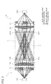
Fig. 2 shows a configuration example of the optical system of the above-described photoelectric sensor. Since this configuration can also applied to a sensor other than the optical fiber type sensor, theoptical fibers Fig. 2 , but alight transmitting element 100 is included in the configuration on the side of the phototransmitter 1 while alight receiving element 200 is included in the configuration on the side of theoptical receiver 2. - A
collimate lens 11 and aprism 12 are incorporated in the phototransmitter 1 of this embodiment, and twopolarizing plates prism 12. The upperpolarizing plate 10P is used for P-polarization, and the lowerpolarizing plate 10S is used for S-polarization. Thepolarizing plates light transmitting window 15 shown inFig. 1B , and the surfaces of thepolarizing plates polarizing plate 10P is referred to as a P-polarizingplate 10P, and thepolarizing plate 10S is referred to as an S-polarizingplate 10S. - In the
optical receiver 2, aprism 22 and alens 21 are provided in order to collect the light, and twopolarizing plates prism 22. Thepolarizing plates light receiving window 25 shown inFig. 1B such that thepolarizing plate 20S for the S-polarization is located above while thepolarizing plate 20P for the P-polarization is located below. Therefore, thepolarizing plates polarizing plate 20S is referred to as an S-polarizingplate 20S, and thepolarizing plate 20P is referred to as a P-polarizingplate 20P. - Dimensions of the
light transmitting window 15 andlight receiving window 25 of the phototransmitter 1 andoptical receiver 2 are unified, and thepolarizing plates optical receiver 2 are disposed opposite to each other, the P-polarizingplate 10P on the side of the phototransmitter 1 and the S-polarizingplate 20S on the side of theoptical receiver 2 are located at the same level, and the S-polarizingplate 10S on the side of the phototransmitter 1 and the P-polarizingplate 10P on the side of theoptimal receiver 2 are located at the same level. - The
light transmitting element 100 outputs the pieces of light vibrated in various directions. After thecollimate lens 11 converts the output light into parallel light, theprism 12 changes an optical axis direction in a range where the P-polarizingplate 10P is irradiated with the light to an obliquely downward direction, and theprism 12 changes an optical axis direction in a range where the S-polarizingplate 10S is irradiated with the light to an obliquely upward direction. Therefore, a vibration direction of the light passing through the P-polarizingplate 10P is unified in a perpendicular direction, and a vibration direction of the light passing through the S-polarizingplate 10S is unified in a horizontal direction. The vibration direction of the light outputted from the phototransmitter 1 is limited to these two directions. - The actual pieces of light that are polarized by and outputted from the
polarizing plates lens 11 andprism 12.Fig. 2 shows a range where the light that reaches a light receiving surface of theoptical receiver 2 to be incident to theoptical receiver 2 travels in each of the P-polarization and S-polarization by different patterns. A main traveling direction of the P-polarized light is expressed by an alternate long and short dash line, and a main traveling direction of the S-polarized light is expressed by a dotted line. - As shown by the patterns, the alternate long and short dash line, and the dotted line of
Fig. 2 , in the photoelectric sensor of this embodiment, the light that is guided to the range corresponding to the P-polarizingplate 20P by traveling in the obliquely downward direction through the P-polarizingplate 10P and the light that is guided to the range corresponding to the S-polarizingplate 20S by traveling in the obliquely upward direction through the S-polarizingplate 10S are incident to theoptical receiver 2. The incident light is collected by theprism 22 and thelens 21 and guided to thelight receiving element 200. - When the
substrate 5 that is the detection target enters a space F (hereinafter referred to as a detection target region F) between the phototransmitter 1 and theoptical receiver 2, among the light incident to theoptical receiver 2, the light from the P-polarizingplate 10P is intercepted by an upper surface of thesubstrate 5, and the light from the S-polarizingplate 10S is intercepted by a lower surface of thesubstrate 5. Accordingly, the light incident to theoptical receiver 2 is largely reduced. Along with this, a signal value of the amount of received light, outputted from thelight receiving element 200, becomes lower than the threshold to set the detection signal to the on-state. - When the
substrate 5 enters the detection target region F, occasionally the pieces of light from thepolarizing plates substrate 5 and guided to theoptical receiver 2. However, because the polarizing plates having characteristics unsuitable to the vibration directions of the pieces of light are provided in positions that the pieces of reflected light reach, the pieces of reflected light can be prevented from being incident to theoptical receiver 2. Therefore, the disturbance in the detection of thesubstrate 5 can be avoided due to the light reflected from the surface of thesubstrate 5. - In the example of
Fig. 2 , the amount of light incident to theoptical receiver 2 is reduced not only at a point where the patterns corresponding to the two kinds of light intersect each other, but also when thesubstrate 5 is located in the range where only the pattern corresponding to one of the two kinds of light is expressed. Thus, the range expressed by each pattern inFig. 2 corresponds to the range where the object (substrate 5) can be detected. Hereinafter, the ranges expressed by the patterns are referred to as a "detection region by P-polarization" and "detection region by S-polarization", respectively, and the both are collectively referred to as a "detection region". - Referring to
Fig. 2 , the detection region by P-polarization and the detection region by S-polarization obliquely traverse the detection target region F and interest each other in the detection target region F. The intersection portion is generated in a range from a boundary position between thepolarizing plates polarizing plates optical receiver 2. Since any detection region has a width corresponding to the polarizing plate, the detection region is distributed over the total width of the detection target region F at any level in a height range (from the highest position of the intersection portion to the lowest position of the intersection portion) corresponding to the intersection portion. Therefore, when thesubstrate 5 is included in the height range corresponding to the intersection portion, the amount of received light of thelight receiving element 200 is reduced by the interceptions of both surfaces of thesubstrate 5, so that thesubstrate 5 can stably be detected. - The detection regions where the two kinds of the P-polarized light and S-polarized light are used are horizontally distributed even in the position above and below the height range corresponding to the intersection portion. Therefore, as shown in
Fig. 2 , when the width of the detection target region F is set according to the width of thesubstrate 5, the light interception state can be generated in the detection region by thesubstrate 5, even if thesubstrate 5 is located at any level in the detection target region F. - The photoelectric sensor is not limited to the usage example shown in
Figs. 1A and 1B , but the photoelectric sensor may be applied to the use in detecting the conveyance of the target objects having various widths. In such cases, the position of the target object is not fixed in the width direction, but the target object may be biased onto the side of the phototransmitter 1 or the side of theoptical receiver 2. When the target object falls within the height range corresponding to the intersection portion of the detection regions, the target object can stably be detected irrespective of the variation of the position in the width direction. - In order to set the detection region distribution to the state shown in
Fig. 2 , it is necessary that the whole surfaces of thepolarizing plates optical receiver 2 is short, the irradiation condition can be satisfied by setting the optical axis direction of each piece of light to the oblique direction. Therefore, the photoelectric sensor of this embodiment can easily deal with the change of the detection distance. -
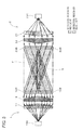
Figs. 3A and 3B each show a broadening range (alternate long and short dash line) of the P-polarized light passing through thepolarizing plate 10P and a broadening range (dotted line) of the S-polarized light passing through thepolarizing plate 10S along with the traveling state of the light incident to theoptical receiver 2 when long and short distances are set between the phototransmitter 1 and theoptical receiver 2. - In the example of
Fig. 3A , the broadening ranges of the P-polarized light and S-polarized light just correspond to the light receiving surface in the position of the light receiving surface. In the example ofFig. 3B , since the distance between the phototransmitter 1 and theoptical receiver 2 is set longer than the example ofFig. 3A , a broadening degree of each piece of light in the position of the light receiving surface is sufficiently larger than the light receiving surface. - As shown in
Figs. 3A and 3B , when the whole light receiving surface of theoptical receiver 2 is irradiated with each of the pieces of light from thepolarizing plates polarizing plates optical receiver 2 and received by thelight receiving element 200. Therefore, dimensions of each detection region can be stabilized. As shown inFig. 3A , the whole light receiving surface can be irradiated with each piece of light from a stage of the short distance between the phototransmitter 1 and theoptical receiver 2 by setting the optical paths of the S-polarized light and P-polarized light obliquely upward and obliquely downward. Accordingly, the photoelectric sensor of this embodiment can deal with both the short-distance detection and the long-distance detection. - Even if the phototransmitter 1 and the
optical receiver 2 come closer to each other than the state shown inFig. 3A , the detection region having the dimensions similar to those ofFigs. 3A and 3B can be secured on the condition that the whole surfaces of thepolarizing plates optical receiver 2 are irradiated with the pieces of light from thepolarizing plates -
Figs. 4A and 4B each show a relationship between the broadening ranges of the pieces of light and the pieces of light incident to theoptical receiver 2 when the pieces of light are outputted without an optical axis being adjusted by aprism 12. In the example ofFig. 4A , the phototransmitter 1 and theoptical receiver 2 are disposed while being away from each other by the same distance as the example ofFig. 3A . In the example ofFig. 4B , the phototransmitter 1 and theoptical receiver 2 are disposed while being away from each other by the same distance as the example ofFig. 3B . - Even if the pieces of light travel from the
polarizing plates optical receiver 2 as shown inFig. 4B . Therefore, the configuration example ofFigs. 4A and 4B can also deal with the long-distance detection. - However, when the distance between the phototransmitter 1 and the
optical receiver 2 is shortened, the whole surfaces of thepolarizing plates Fig. 4A . Therefore, the detection region is reduced, and a region where thesubstrate 5 cannot be detected is generated in the detection target region F as expressed by rectangular frames NG1 and NG2 ofFig. 4A . - Accordingly, in order to deal with both the short-distance detection and the long-distance detection, as shown in
Fig. 2 andFigs. 3A and 3B , it is necessary to adopt the method for outputting the two kinds of light toward the obliquely upward direction and the obliquely downward direction. When the method is adopted, the configuration of the optical system is not limited to the examples ofFig. 2 andFigs. 3A and 3B , but the optical system may be configured as shown inFigs. 5 to 9 . - Hereinafter, embodiments will be described with reference to the drawing. In each embodiment, the configuration similar to that of the previous embodiment is designated by the same reference numeral, and the description thereof is not given or simplified.
- The two kinds of light used to detect the object is not limited to the light whose polarization direction is aligned, but the pieces of light having different wavelength ranges can also be used. In embodiments of
Figs. 5 and6 , the detection by the principle similar to that ofFig. 2 is performed using the pieces of light having the different wavelength ranges. - In the embodiment shown in
Fig. 5 , red light extractingcolor filters plates optical receiver 2, and blue light extractingcolor filters plates light transmitting element 100. - Accordingly, the red light is outputted obliquely downward from an upper half region of the light transmitting surface of the phototransmitter 1 and the blue light is outputted obliquely upward from a lower half region. In the pieces of color light, the red light that is guided to the range where the
color filter 20R of theoptical receiver 2 is disposed and the blue light that is guided to the range where thecolor filter 20B is disposed are guided to thelight receiving element 200. - In the embodiment shown in
Fig. 6 , alight transmitting element 100R that outputs the red light and alight transmitting element 100B that outputs the blue light are provided in the phototransmitter 1 without providing thecolor filters light transmitting elements prism 12 through thecollimate lens 11 R and 11 B, respectively. In such cases, thelight transmitting elements - In the embodiment of
Fig. 6 , in the phototransmitter 1, thelight transmitting elements light transmitting elements
Even in the example ofFig. 2 in which the polarizing plate is used and the example ofFig. 5 in which the color filter is used, the light source can be divided in each output direction, and therefore the intensity of the output light can be enhanced to improve the stability of the detection. - In the embodiment shown in
Fig. 7 , similarly to the embodiment ofFig. 2 , the detection region is set using thepolarizing plates collective lenses 21 P and 21 S are provided in theoptical receiver 2 to individual collect the P-polarized light and the S-polarized light, and the collected P-polarized light and the collected S-polarized light are guided tolight receiving elements - Although not shown in
Fig. 7 , in this embodiment, the signal processing device 3 individually checks the amounts of received light obtained by thelight receiving elements - According to the above-described configuration, even when the object enters only one of the detection regions by P-polarization and the detection region by S-polarization, the object can be detected based on the reduction of the amount of received light in the detection region. Therefore, the detection sensitivity can be enhanced so that even a small object can be accurately detected.
- When the detection is performed using the two kinds of color light as shown in the examples of
Figs. 5 and6 , each piece of color light is guided to the individual light receiving element similarly to the example ofFig. 7 , and the checking processing of the amount of received light can be performed in each light receiving element. -
Figs. 8 and9 show configuration examples an optical system of a reflection type photoelectric sensor.
The photoelectric sensor of the embodiment ofFig. 8 includes asensor head 310 and amirror unit 320. Thelight transmitting element 100 and thelight receiving element 200 are accommodated in thesensor head 310. Themirror unit 320 includes areturn reflector plate 24. The P-polarizingplate 10P and the S-polarizingplate 10S are disposed in front of thesensor head 310 in the state similar to that of the phototransmitter 1 of this embodiment ofFig. 2 . Theprism 12 and thecollimate lens 11 are disposed in thesensor head 310 in the state similar to that of the phototransmitter 1 of this embodiment ofFig. 2 , and ahalf mirror 14 is provided at the back of thecollimate lens 11, - In the
mirror unit 320, the S-polarizingplate 20S and the P-polarizingplate 20P are vertically arrayed in the whole surface of a holder (not shown) in which thereturn reflector plate 24 is fitted. When themirror unit 320 and thesensor head 310 are disposed opposite to each other, the P-polarizingplate 10P of thesensor head 310 and the S-polarizingplate 20S of themirror unit 320 are disposed at the same level, and the S-polarizingplate 10S of the sensor head and the P-polarizingplate 20P of the mirror unit are disposed at the same level. - In the above-described configuration, the
light transmitting element 100 outputs pieces of light vibrated in various directions. The pieces of light are guided to thecollimate lens 11 through thehalf mirror 14 and changed into the pieces of light along the horizontal direction. The P-polarized light traveling obliquely downward and the S-polarized light traveling obliquely upward are outputted by theprism 12 and thepolarizing plates - In this embodiment as well, the
sensor head 310 and themirror unit 320 are disposed while being away from each other by the distance similar to the distance between the phototransmitter 1 and theoptical receiver 2 ofFig. 3A , which allows the whole surfaces of the twopolarizing plates mirror unit 320 to be irradiated with the pieces of light from thepolarizing plates polarizing plate 20P is irradiated and the S-polarized light with which thepolarizing plate 20S is irradiated are guided to thereturn reflector plate 24. - The
return reflector plate 24 has a function of reflecting the irradiation light to an irradiation direction, and vibration regularity of the light collapses by the reflection. Therefore, the pieces of reflected light are vibrated in various directions. In the pieces of light reflected toward thepolarizing plate 20P, the P-polarized light travels toward thepolarizing plate 10P on the side of thesensor head 310 through thepolarizing plate 20P, and the P-polarized light is incident to thesensor head 310 through thepolarizing plate 10P. In the pieces of light reflected toward thepolarizing plate 20S, the S-polarized light travels toward thepolarizing plate 10S on the side of thesensor head 310 through thepolarizing plate 20S, and the S-polarized light is incident to thesensor head 310 through thepolarizing plate 10S. - The light incident to the
sensor head 310 is guided to thelight receiving element 200 through thelight half mirror 14 after being collected by theprism 12 and thelens 11, Therefore, a range where the light reciprocating between thesensor head 310 and themirror unit 320 travels constitutes the detection region, and thesubstrate 5 can be detected in the range similar to that of the transmission type photoelectric sensor shown inFig. 2 . -
Fig. 9 shows a second configuration example of the reflection type photoelectric sensor.
In this embodiment, themirror unit 302 is similar to that of the example ofFig. 8 . However, thehalf mirror 14, thelight transmitting element 100, and thelight receiving element 200 are not provided in thesensor head 310, and a coaxial typeoptical fiber 300 is drawn from the signal processing device 3. - The
optical fiber 300 is disposed while a leading end of theoptical fiber 300 is aligned with a focal position of thelens 11. As shown in an enlarged view on the lower left ofFig. 9 , in theoptical fiber 300, a plurality oflight receiving fibers 302 are disposed around alight transmitting fiber 301 having a large diameter, and thelight receiving fibers 302 and thelight transmitting fiber 301 are fixed by acoating material 303. - The light outputted from the light transmitting element 100 (not shown in
Fig. 9 ) of the signal processing device 3 is guided to thesensor head 310 by thelight transmitting fiber 301 and outputted to themirror unit 320 in the principle similar to that of the example shown inFig. 8 . The reflected light is returned from themirror unit 320 onto the side of thesensor head 310 in the principle similar to that of the example shown inFig. 8 . - The light returned to the
sensor head 310 is collected by theprism 12 and thelens 11 and guided to theoptical fiber 300, and the light is incident to thelight receiving fiber 302. The light incident to thelight receiving fiber 302 is guided to the light receiving element 200 (not shown inFig. 9 ) of the signal processing device 3. - In the embodiments of
Figs. 8 and9 of the reflection type photoelectric sensor, since thepolarizing plates sensor head 310 and themirror unit 320, a ratio of the amount of received light to the amount of output light becomes smaller than that of the transmission type photoelectric sensor. However, for example, the light interception state can sufficiently be detected by the method for enhancing the light emission intensity of the light transmitting element. When the configuration similar to that ofFigs. 8 and9 is implemented using thecolor filters Fig. 5 instead of thepolarizing plates - In the embodiments described above, the region where the two kinds of light are outputted in the phototransmitter 1 or the optical filters (the
polarizing plates color filters
Claims (8)
- A photoelectric sensor characterized by comprising:a phototransmitter (1) that outputs light toward a detection target region of an object (5);an optical receiver (2) that receives the light outputted from the phototrassmitter (1);a signal processing unit (3) that outputs a signal indicating that the object (5) is detected in response to a decrease of an amount of light received by the optical receiver (2); andtwo first optical filters (10R, 10B, 20R, 20B) that are provided between the phototransmitter (1) and the optical receiver (2) to transmit only pieces of light having specific characteristics, whereinin the phototransmitter (1), two kinds of light having different characteristics and that do not interfere with each other are outputted from output regions in the light transmitting surface,one of the two first optical filters (10R, 10B, 20R, 20B) has a characteristic of transmitting only one of the two kinds of light and the other of the first optical filters (10R, 10B, 20R, 20B) has a characteristic of transmitting only the other of the two kinds of light,the two first optical filters (10R, 10B, 20R, 20B) are disposed opposite to output regions of the pieces of light different from the pieces of light of a selecting target while located across a detection target region, andoutput directions of the two kinds of light are fixed such that whole surfaces of the first optical filters (10R, 10B, 20R, 20B) corresponding to the characteristics are irradiated with the two kinds of light from the phototransmitter (1) when the two first optical filters (10R, 10B, 20R, 20B) are disposed in a light transmitting surface while located away from each other by a predetermined distance or more.
- The photoelectric sensor according to claim 1, characterized in that an optical axis setting unit is provided in the phototransmitter (1), the optical axis setting unit changing an optical axis direction of the light from a light source to the output regions of the two kinds of light to a direction in which the first optical filters (10R, 10B, 20R, 20B) are disposed such that the light obliquely traverses the detection target region toward the positions in which the first optical filters (10R, 10B, 20R, 20B) are disposed.
- The photoelectric sensor according to claim 1, characterized in that the two first optical filters (10R, 108, 20R, 20B) is integrally provided in the optical receiver (2) while arrayed in parallel in a light receiving surface of the optical receiver (2), and
the optical receiver (2) is disposed opposite to the phototransmitter (1) along with the two first optical filters (10R, 10B, 20R, 20B) to receive the pieces of light passing through the first optical filters (10R, 108, 20R, 208). - The photoelectric sensor according to claim 3, characterized in that the optical receiver (2) is configured to individually collect the pieces of light passing through the two first optical filters (10R, 10B, 20R, 208) and individually guide the pieces of collected light to light receiving elements (200, 200P, 200S).
- The photoelectric sensor according to claim 1, characterized in that the phototransmitter (1) and the optical receiver (2) are provided in the same housing on an assumption that a return reflector plate (24) is provided on an opposite side to the detection target region with respect to the pair of optical filters (10R, 10B, 20R, 20B),
in the housing, a surface that is opposite to the detection target region acts as a light transmitting surface and a light receiving surface, and
the optical receiver (2) receives the light that is returned through the two first optical filters (10R, 10B, 20R, 20B) after being reflected by the return reflector plate (24) in the two kinds of light that are outputted from the phototransmitter (1) to pass through the optical filters (10R, 10B, 20R, 20B). - The photoelectric sensor according to any of claims 1, characterized in that two kinds of light vibrated in specific directions and having different vibration directions are outputted from a light transmitting surface of the phototransmitter (1), and
two polarizing plates (10P, 10S, 20P, 20S) is disposed as the two first optical filters (10R, 10B, 20R, 20B) opposite to the output regions of the pieces of light that are not the selection target while located across a detection target region, the two polarizing plates (10P, 10S, 20P, 20S) being directed to the selection of the vibration directions of the two kinds of light. - The photoelectric sensor according to any of claims 1, characterized in that two kinds of light having different wavelength ranges are outputted from a light transmitting surface of the phototransmitter (1),
the two first optical filters (10R, 10B, 20R, 20B) are directed to the selection of the wavelength ranges corresponding to the two kinds of light, and
the first optical filters (10R, 10B, 20R, 20B) are disposed opposite to the output regions of the pieces of light that are not the selection target while located across a detection target region. - The photoelectric sensor according to any of claims 1, characterized in that, in the phototransmitter (1), two second optical filters (10R, 10B, 20R, 20B) including characteristics identical to those of the first optical filters (10R, 10B, 20R, 20B) are arrayed along the light transmitting surface so as to be opposite to the first optical filters having different characteristics, the second optical filters (10R, 10B, 20R, 20B) being located across the detection target region, and
the pieces of the light passing through the two second optical filters (10R, 10B, 20R, 20B) of the phototransmitter (1) are outputted as the two kinds of light.
Applications Claiming Priority (1)
| Application Number | Priority Date | Filing Date | Title |
|---|---|---|---|
| JP2009256903A JP5458813B2 (en) | 2009-11-10 | 2009-11-10 | Photoelectric sensor |
Publications (2)
| Publication Number | Publication Date |
|---|---|
| EP2320192A1 true EP2320192A1 (en) | 2011-05-11 |
| EP2320192B1 EP2320192B1 (en) | 2014-12-03 |
Family
ID=43569499
Family Applications (1)
| Application Number | Title | Priority Date | Filing Date |
|---|---|---|---|
| EP20100189644 Active EP2320192B1 (en) | 2009-11-10 | 2010-11-02 | Photoelectric Sensor |
Country Status (5)
| Country | Link |
|---|---|
| US (1) | US8890054B2 (en) |
| EP (1) | EP2320192B1 (en) |
| JP (1) | JP5458813B2 (en) |
| KR (1) | KR101246394B1 (en) |
| CN (1) | CN102052929B (en) |
Cited By (1)
| Publication number | Priority date | Publication date | Assignee | Title |
|---|---|---|---|---|
| WO2015183299A1 (en) * | 2014-05-30 | 2015-12-03 | Hewlett-Packard Development Company, L.P. | Positional input on displays |
Families Citing this family (3)
| Publication number | Priority date | Publication date | Assignee | Title |
|---|---|---|---|---|
| JP6117502B2 (en) * | 2012-09-11 | 2017-04-19 | Necプラットフォームズ株式会社 | Object detection device, mechatronic device, and object detection method |
| JP2014123455A (en) * | 2012-12-20 | 2014-07-03 | Azbil Corp | Photoelectronic sensor |
| US9341466B1 (en) * | 2014-12-04 | 2016-05-17 | Xerox Corporation | Sheet height sensor using movable and stationary mirrors |
Citations (5)
| Publication number | Priority date | Publication date | Assignee | Title |
|---|---|---|---|---|
| JPH0669323A (en) | 1992-08-19 | 1994-03-11 | Tokyo Electron Ltd | Wafer detection device and wafer positioning device |
| JP2007258386A (en) | 2006-03-23 | 2007-10-04 | Juki Corp | Transferred board detecting device |
| US20080273758A1 (en) * | 2005-11-14 | 2008-11-06 | Oliver Fuchs | Apparatus and method for monitoring a spatial area, in particular for safeguarding a hazardous area of an automatically operated installation |
| EP2042854A2 (en) * | 2007-09-28 | 2009-04-01 | Rockwell Automation Technologies, Inc. | Near infrared sensor system with nano-imprinted wire-grid polarizers and method using the same |
| JP2009216489A (en) | 2008-03-10 | 2009-09-24 | Yamatake Corp | Photosensor device and workpiece position detecting method using the same |
Family Cites Families (19)
| Publication number | Priority date | Publication date | Assignee | Title |
|---|---|---|---|---|
| US734575A (en) | 1903-03-30 | 1903-07-28 | Reinhold Krubetke | Shutter-fastener. |
| US847488A (en) | 1906-07-02 | 1907-03-19 | Carl Metterhausen | Mechanism for operating double sliding doors. |
| JPS5377362U (en) * | 1976-12-01 | 1978-06-28 | ||
| JPS5821295A (en) | 1981-07-29 | 1983-02-08 | セイコーインスツルメンツ株式会社 | Picture display unit |
| JPS59126437U (en) * | 1983-02-15 | 1984-08-25 | オムロン株式会社 | photoelectric switch |
| CH667340A5 (en) * | 1985-04-30 | 1988-09-30 | Cerberus Ag | PHOTOELECTRIC BARRIER. |
| US4725601A (en) * | 1985-06-04 | 1988-02-16 | Fujisawa Pharmaceutical Co., Ltd. | Certain imidazo[1,2-a]pyridines useful in the treatment of ulcers |
| JPH072742B2 (en) | 1985-08-13 | 1995-01-18 | 住友化学工業株式会社 | 4H-1,4-diazabicyclo [3.3.0] oct-6-ene-3,8-dione derivative and herbicide containing it as an active ingredient |
| JPS6429743U (en) * | 1987-08-13 | 1989-02-22 | ||
| US4847488A (en) * | 1987-12-23 | 1989-07-11 | Cerberus Ag | Sabotage resistant light barrier wherein radiation is polarized into two opposite types of polarization |
| JPH0317583U (en) * | 1989-07-03 | 1991-02-21 | ||
| US5319216A (en) | 1991-07-26 | 1994-06-07 | Tokyo Electron Limited | Substrate detector with light emitting and receiving elements arranged in staggered fashion and a polarization filter |
| JP2984958B2 (en) | 1991-07-26 | 1999-11-29 | 東京エレクトロン株式会社 | Substrate single wafer detection system |
| JP4114771B2 (en) * | 2002-03-20 | 2008-07-09 | サンクス株式会社 | Reflector and reflector reflective photoelectric switch |
| JP2004071366A (en) * | 2002-08-07 | 2004-03-04 | Omron Corp | Photoelectric sensor |
| JP3669352B2 (en) * | 2002-09-11 | 2005-07-06 | オムロン株式会社 | Photoelectric sensor |
| JP2005227121A (en) * | 2004-02-13 | 2005-08-25 | Omron Corp | Countermeasures for preventing mutual interference in photoelectric switch |
| JP2005241340A (en) * | 2004-02-25 | 2005-09-08 | Sharp Corp | Multi-range finding device |
| JP5282418B2 (en) | 2008-03-10 | 2013-09-04 | 株式会社ニコン | camera |
-
2009
- 2009-11-10 JP JP2009256903A patent/JP5458813B2/en active Active
-
2010
- 2010-11-02 EP EP20100189644 patent/EP2320192B1/en active Active
- 2010-11-03 KR KR1020100108637A patent/KR101246394B1/en active IP Right Grant
- 2010-11-08 US US12/941,594 patent/US8890054B2/en active Active
- 2010-11-10 CN CN201010546243.7A patent/CN102052929B/en active Active
Patent Citations (5)
| Publication number | Priority date | Publication date | Assignee | Title |
|---|---|---|---|---|
| JPH0669323A (en) | 1992-08-19 | 1994-03-11 | Tokyo Electron Ltd | Wafer detection device and wafer positioning device |
| US20080273758A1 (en) * | 2005-11-14 | 2008-11-06 | Oliver Fuchs | Apparatus and method for monitoring a spatial area, in particular for safeguarding a hazardous area of an automatically operated installation |
| JP2007258386A (en) | 2006-03-23 | 2007-10-04 | Juki Corp | Transferred board detecting device |
| EP2042854A2 (en) * | 2007-09-28 | 2009-04-01 | Rockwell Automation Technologies, Inc. | Near infrared sensor system with nano-imprinted wire-grid polarizers and method using the same |
| JP2009216489A (en) | 2008-03-10 | 2009-09-24 | Yamatake Corp | Photosensor device and workpiece position detecting method using the same |
Cited By (3)
| Publication number | Priority date | Publication date | Assignee | Title |
|---|---|---|---|---|
| WO2015183299A1 (en) * | 2014-05-30 | 2015-12-03 | Hewlett-Packard Development Company, L.P. | Positional input on displays |
| TWI638292B (en) * | 2014-05-30 | 2018-10-11 | 惠普發展公司有限責任合夥企業 | Positional input on displays |
| US10353488B2 (en) | 2014-05-30 | 2019-07-16 | Hewlett-Packard Development Company, L.P. | Positional input on displays |
Also Published As
| Publication number | Publication date |
|---|---|
| KR20110052467A (en) | 2011-05-18 |
| CN102052929B (en) | 2014-10-29 |
| CN102052929A (en) | 2011-05-11 |
| EP2320192B1 (en) | 2014-12-03 |
| KR101246394B1 (en) | 2013-03-21 |
| US8890054B2 (en) | 2014-11-18 |
| JP5458813B2 (en) | 2014-04-02 |
| US20110272563A1 (en) | 2011-11-10 |
| JP2011103187A (en) | 2011-05-26 |
Similar Documents
| Publication | Publication Date | Title |
|---|---|---|
| EP1313222B1 (en) | Method and apparatus for self-monitoring of proximity sensors | |
| US8890054B2 (en) | Photoelectric sensor used for detection of thin objects | |
| KR101640989B1 (en) | Limited area reflective optical sensor and electronic device | |
| US6130437A (en) | Sensor and detection system having wide diverging beam optics | |
| CN103576133A (en) | Distance measuring system | |
| EP1471565B1 (en) | Mapping device for semiconductor wafers | |
| CN103907000A (en) | Sensor for checking value documents | |
| EP1493022A1 (en) | Imaging method and apparatus | |
| US20030174329A1 (en) | System and method for aligning a first optical device with an input port of a second optical device | |
| US20220244556A1 (en) | Optical detection system for improved alignment | |
| US9874705B2 (en) | Optical waveguide module | |
| CN213042338U (en) | Adhesive tape detection module and currency detection device using same | |
| JP4186185B2 (en) | Object detection method | |
| KR100611129B1 (en) | Photoelectric sensor | |
| WO2017007256A1 (en) | Focusing point detection device | |
| JPH10218430A (en) | Detecting device for carrying medium | |
| JP2004037461A (en) | Device for optically measuring distance | |
| EP3757604B1 (en) | Photoelectric sensor with coaxial emission and receiving optical paths | |
| US20040190908A1 (en) | Optical transmission device | |
| US3643103A (en) | Light-conducting member for photoelectric code sensor | |
| JPS60117116A (en) | Photosensor | |
| CN112184984A (en) | Currency detector with adhesive tape detection function | |
| KR20110122940A (en) | Reflective type optical sensor for reflector | |
| CN112240745A (en) | Light receiver, light projector, and photoelectric sensor | |
| JPWO2020039478A1 (en) | Chromatographic detector |
Legal Events
| Date | Code | Title | Description |
|---|---|---|---|
| PUAI | Public reference made under article 153(3) epc to a published international application that has entered the european phase |
Free format text: ORIGINAL CODE: 0009012 |
|
| AK | Designated contracting states |
Kind code of ref document: A1 Designated state(s): AL AT BE BG CH CY CZ DE DK EE ES FI FR GB GR HR HU IE IS IT LI LT LU LV MC MK MT NL NO PL PT RO RS SE SI SK SM TR |
|
| AX | Request for extension of the european patent |
Extension state: BA ME |
|
| 17P | Request for examination filed |
Effective date: 20111109 |
|
| 17Q | First examination report despatched |
Effective date: 20130515 |
|
| GRAP | Despatch of communication of intention to grant a patent |
Free format text: ORIGINAL CODE: EPIDOSNIGR1 |
|
| RIC1 | Information provided on ipc code assigned before grant |
Ipc: G01B 11/02 20060101ALI20140521BHEP Ipc: G01V 8/12 20060101ALI20140521BHEP Ipc: G01V 8/20 20060101ALI20140521BHEP Ipc: G01B 11/00 20060101AFI20140521BHEP |
|
| INTG | Intention to grant announced |
Effective date: 20140620 |
|
| RAP1 | Party data changed (applicant data changed or rights of an application transferred) |
Owner name: OMRON CORPORATION |
|
| RIN1 | Information on inventor provided before grant (corrected) |
Inventor name: OGAKI, SHINJI Inventor name: GONDO, KIYOHIKO Inventor name: KATAYAMA, TETSUYUKI Inventor name: KATO, KATSUHIKO |
|
| GRAP | Despatch of communication of intention to grant a patent |
Free format text: ORIGINAL CODE: EPIDOSNIGR1 |
|
| GRAS | Grant fee paid |
Free format text: ORIGINAL CODE: EPIDOSNIGR3 |
|
| GRAA | (expected) grant |
Free format text: ORIGINAL CODE: 0009210 |
|
| INTG | Intention to grant announced |
Effective date: 20141014 |
|
| AK | Designated contracting states |
Kind code of ref document: B1 Designated state(s): AL AT BE BG CH CY CZ DE DK EE ES FI FR GB GR HR HU IE IS IT LI LT LU LV MC MK MT NL NO PL PT RO RS SE SI SK SM TR |
|
| REG | Reference to a national code |
Ref country code: GB Ref legal event code: FG4D |
|
| REG | Reference to a national code |
Ref country code: CH Ref legal event code: EP Ref country code: AT Ref legal event code: REF Ref document number: 699618 Country of ref document: AT Kind code of ref document: T Effective date: 20141215 |
|
| REG | Reference to a national code |
Ref country code: IE Ref legal event code: FG4D |
|
| REG | Reference to a national code |
Ref country code: DE Ref legal event code: R096 Ref document number: 602010020668 Country of ref document: DE Effective date: 20150115 |
|
| REG | Reference to a national code |
Ref country code: NL Ref legal event code: VDEP Effective date: 20141203 |
|
| REG | Reference to a national code |
Ref country code: AT Ref legal event code: MK05 Ref document number: 699618 Country of ref document: AT Kind code of ref document: T Effective date: 20141203 |
|
| PG25 | Lapsed in a contracting state [announced via postgrant information from national office to epo] |
Ref country code: LT Free format text: LAPSE BECAUSE OF FAILURE TO SUBMIT A TRANSLATION OF THE DESCRIPTION OR TO PAY THE FEE WITHIN THE PRESCRIBED TIME-LIMIT Effective date: 20141203 Ref country code: ES Free format text: LAPSE BECAUSE OF FAILURE TO SUBMIT A TRANSLATION OF THE DESCRIPTION OR TO PAY THE FEE WITHIN THE PRESCRIBED TIME-LIMIT Effective date: 20141203 Ref country code: NL Free format text: LAPSE BECAUSE OF FAILURE TO SUBMIT A TRANSLATION OF THE DESCRIPTION OR TO PAY THE FEE WITHIN THE PRESCRIBED TIME-LIMIT Effective date: 20141203 Ref country code: FI Free format text: LAPSE BECAUSE OF FAILURE TO SUBMIT A TRANSLATION OF THE DESCRIPTION OR TO PAY THE FEE WITHIN THE PRESCRIBED TIME-LIMIT Effective date: 20141203 Ref country code: NO Free format text: LAPSE BECAUSE OF FAILURE TO SUBMIT A TRANSLATION OF THE DESCRIPTION OR TO PAY THE FEE WITHIN THE PRESCRIBED TIME-LIMIT Effective date: 20150303 |
|
| REG | Reference to a national code |
Ref country code: LT Ref legal event code: MG4D |
|
| PG25 | Lapsed in a contracting state [announced via postgrant information from national office to epo] |
Ref country code: LV Free format text: LAPSE BECAUSE OF FAILURE TO SUBMIT A TRANSLATION OF THE DESCRIPTION OR TO PAY THE FEE WITHIN THE PRESCRIBED TIME-LIMIT Effective date: 20141203 Ref country code: SE Free format text: LAPSE BECAUSE OF FAILURE TO SUBMIT A TRANSLATION OF THE DESCRIPTION OR TO PAY THE FEE WITHIN THE PRESCRIBED TIME-LIMIT Effective date: 20141203 Ref country code: CY Free format text: LAPSE BECAUSE OF FAILURE TO SUBMIT A TRANSLATION OF THE DESCRIPTION OR TO PAY THE FEE WITHIN THE PRESCRIBED TIME-LIMIT Effective date: 20141203 Ref country code: GR Free format text: LAPSE BECAUSE OF FAILURE TO SUBMIT A TRANSLATION OF THE DESCRIPTION OR TO PAY THE FEE WITHIN THE PRESCRIBED TIME-LIMIT Effective date: 20150304 Ref country code: RS Free format text: LAPSE BECAUSE OF FAILURE TO SUBMIT A TRANSLATION OF THE DESCRIPTION OR TO PAY THE FEE WITHIN THE PRESCRIBED TIME-LIMIT Effective date: 20141203 Ref country code: AT Free format text: LAPSE BECAUSE OF FAILURE TO SUBMIT A TRANSLATION OF THE DESCRIPTION OR TO PAY THE FEE WITHIN THE PRESCRIBED TIME-LIMIT Effective date: 20141203 Ref country code: HR Free format text: LAPSE BECAUSE OF FAILURE TO SUBMIT A TRANSLATION OF THE DESCRIPTION OR TO PAY THE FEE WITHIN THE PRESCRIBED TIME-LIMIT Effective date: 20141203 |
|
| PG25 | Lapsed in a contracting state [announced via postgrant information from national office to epo] |
Ref country code: EE Free format text: LAPSE BECAUSE OF FAILURE TO SUBMIT A TRANSLATION OF THE DESCRIPTION OR TO PAY THE FEE WITHIN THE PRESCRIBED TIME-LIMIT Effective date: 20141203 Ref country code: CZ Free format text: LAPSE BECAUSE OF FAILURE TO SUBMIT A TRANSLATION OF THE DESCRIPTION OR TO PAY THE FEE WITHIN THE PRESCRIBED TIME-LIMIT Effective date: 20141203 Ref country code: PT Free format text: LAPSE BECAUSE OF FAILURE TO SUBMIT A TRANSLATION OF THE DESCRIPTION OR TO PAY THE FEE WITHIN THE PRESCRIBED TIME-LIMIT Effective date: 20150403 Ref country code: RO Free format text: LAPSE BECAUSE OF FAILURE TO SUBMIT A TRANSLATION OF THE DESCRIPTION OR TO PAY THE FEE WITHIN THE PRESCRIBED TIME-LIMIT Effective date: 20141203 Ref country code: SK Free format text: LAPSE BECAUSE OF FAILURE TO SUBMIT A TRANSLATION OF THE DESCRIPTION OR TO PAY THE FEE WITHIN THE PRESCRIBED TIME-LIMIT Effective date: 20141203 |
|
| PG25 | Lapsed in a contracting state [announced via postgrant information from national office to epo] |
Ref country code: PL Free format text: LAPSE BECAUSE OF FAILURE TO SUBMIT A TRANSLATION OF THE DESCRIPTION OR TO PAY THE FEE WITHIN THE PRESCRIBED TIME-LIMIT Effective date: 20141203 Ref country code: IS Free format text: LAPSE BECAUSE OF FAILURE TO SUBMIT A TRANSLATION OF THE DESCRIPTION OR TO PAY THE FEE WITHIN THE PRESCRIBED TIME-LIMIT Effective date: 20150403 |
|
| REG | Reference to a national code |
Ref country code: DE Ref legal event code: R097 Ref document number: 602010020668 Country of ref document: DE |
|
| PLBE | No opposition filed within time limit |
Free format text: ORIGINAL CODE: 0009261 |
|
| STAA | Information on the status of an ep patent application or granted ep patent |
Free format text: STATUS: NO OPPOSITION FILED WITHIN TIME LIMIT |
|
| PG25 | Lapsed in a contracting state [announced via postgrant information from national office to epo] |
Ref country code: DK Free format text: LAPSE BECAUSE OF FAILURE TO SUBMIT A TRANSLATION OF THE DESCRIPTION OR TO PAY THE FEE WITHIN THE PRESCRIBED TIME-LIMIT Effective date: 20141203 |
|
| 26N | No opposition filed |
Effective date: 20150904 |
|
| PG25 | Lapsed in a contracting state [announced via postgrant information from national office to epo] |
Ref country code: IT Free format text: LAPSE BECAUSE OF FAILURE TO SUBMIT A TRANSLATION OF THE DESCRIPTION OR TO PAY THE FEE WITHIN THE PRESCRIBED TIME-LIMIT Effective date: 20141203 |
|
| PG25 | Lapsed in a contracting state [announced via postgrant information from national office to epo] |
Ref country code: SI Free format text: LAPSE BECAUSE OF FAILURE TO SUBMIT A TRANSLATION OF THE DESCRIPTION OR TO PAY THE FEE WITHIN THE PRESCRIBED TIME-LIMIT Effective date: 20141203 |
|
| PG25 | Lapsed in a contracting state [announced via postgrant information from national office to epo] |
Ref country code: BE Free format text: LAPSE BECAUSE OF FAILURE TO SUBMIT A TRANSLATION OF THE DESCRIPTION OR TO PAY THE FEE WITHIN THE PRESCRIBED TIME-LIMIT Effective date: 20141203 |
|
| PG25 | Lapsed in a contracting state [announced via postgrant information from national office to epo] |
Ref country code: LU Free format text: LAPSE BECAUSE OF FAILURE TO SUBMIT A TRANSLATION OF THE DESCRIPTION OR TO PAY THE FEE WITHIN THE PRESCRIBED TIME-LIMIT Effective date: 20151102 Ref country code: MC Free format text: LAPSE BECAUSE OF FAILURE TO SUBMIT A TRANSLATION OF THE DESCRIPTION OR TO PAY THE FEE WITHIN THE PRESCRIBED TIME-LIMIT Effective date: 20141203 |
|
| REG | Reference to a national code |
Ref country code: CH Ref legal event code: PL |
|
| GBPC | Gb: european patent ceased through non-payment of renewal fee |
Effective date: 20151102 |
|
| PG25 | Lapsed in a contracting state [announced via postgrant information from national office to epo] |
Ref country code: CH Free format text: LAPSE BECAUSE OF NON-PAYMENT OF DUE FEES Effective date: 20151130 Ref country code: LI Free format text: LAPSE BECAUSE OF NON-PAYMENT OF DUE FEES Effective date: 20151130 |
|
| REG | Reference to a national code |
Ref country code: IE Ref legal event code: MM4A |
|
| REG | Reference to a national code |
Ref country code: FR Ref legal event code: ST Effective date: 20160729 |
|
| PG25 | Lapsed in a contracting state [announced via postgrant information from national office to epo] |
Ref country code: GB Free format text: LAPSE BECAUSE OF NON-PAYMENT OF DUE FEES Effective date: 20151102 Ref country code: IE Free format text: LAPSE BECAUSE OF NON-PAYMENT OF DUE FEES Effective date: 20151102 |
|
| PG25 | Lapsed in a contracting state [announced via postgrant information from national office to epo] |
Ref country code: FR Free format text: LAPSE BECAUSE OF NON-PAYMENT OF DUE FEES Effective date: 20151130 |
|
| PG25 | Lapsed in a contracting state [announced via postgrant information from national office to epo] |
Ref country code: SM Free format text: LAPSE BECAUSE OF FAILURE TO SUBMIT A TRANSLATION OF THE DESCRIPTION OR TO PAY THE FEE WITHIN THE PRESCRIBED TIME-LIMIT Effective date: 20141203 Ref country code: HU Free format text: LAPSE BECAUSE OF FAILURE TO SUBMIT A TRANSLATION OF THE DESCRIPTION OR TO PAY THE FEE WITHIN THE PRESCRIBED TIME-LIMIT; INVALID AB INITIO Effective date: 20101102 Ref country code: BG Free format text: LAPSE BECAUSE OF FAILURE TO SUBMIT A TRANSLATION OF THE DESCRIPTION OR TO PAY THE FEE WITHIN THE PRESCRIBED TIME-LIMIT Effective date: 20141203 |
|
| PG25 | Lapsed in a contracting state [announced via postgrant information from national office to epo] |
Ref country code: TR Free format text: LAPSE BECAUSE OF FAILURE TO SUBMIT A TRANSLATION OF THE DESCRIPTION OR TO PAY THE FEE WITHIN THE PRESCRIBED TIME-LIMIT Effective date: 20141203 Ref country code: MT Free format text: LAPSE BECAUSE OF FAILURE TO SUBMIT A TRANSLATION OF THE DESCRIPTION OR TO PAY THE FEE WITHIN THE PRESCRIBED TIME-LIMIT Effective date: 20141203 |
|
| PG25 | Lapsed in a contracting state [announced via postgrant information from national office to epo] |
Ref country code: MK Free format text: LAPSE BECAUSE OF FAILURE TO SUBMIT A TRANSLATION OF THE DESCRIPTION OR TO PAY THE FEE WITHIN THE PRESCRIBED TIME-LIMIT Effective date: 20141203 |
|
| PG25 | Lapsed in a contracting state [announced via postgrant information from national office to epo] |
Ref country code: AL Free format text: LAPSE BECAUSE OF FAILURE TO SUBMIT A TRANSLATION OF THE DESCRIPTION OR TO PAY THE FEE WITHIN THE PRESCRIBED TIME-LIMIT Effective date: 20141203 |
|
| PGFP | Annual fee paid to national office [announced via postgrant information from national office to epo] |
Ref country code: DE Payment date: 20230929 Year of fee payment: 14 |