EP2316784B1 - Hohlraumverbindungsstruktur, die einen oder mehrere aufsteigende Leiter an den Wänden des Hohlraums aufweist, und entsprechendes Herstellungsverfahren - Google Patents
Hohlraumverbindungsstruktur, die einen oder mehrere aufsteigende Leiter an den Wänden des Hohlraums aufweist, und entsprechendes Herstellungsverfahren Download PDFInfo
- Publication number
- EP2316784B1 EP2316784B1 EP10189285.9A EP10189285A EP2316784B1 EP 2316784 B1 EP2316784 B1 EP 2316784B1 EP 10189285 A EP10189285 A EP 10189285A EP 2316784 B1 EP2316784 B1 EP 2316784B1
- Authority
- EP
- European Patent Office
- Prior art keywords
- cavity
- support
- conductive
- figures
- grooves
- Prior art date
- Legal status (The legal status is an assumption and is not a legal conclusion. Google has not performed a legal analysis and makes no representation as to the accuracy of the status listed.)
- Not-in-force
Links
Images


Classifications
-
- B—PERFORMING OPERATIONS; TRANSPORTING
- B81—MICROSTRUCTURAL TECHNOLOGY
- B81B—MICROSTRUCTURAL DEVICES OR SYSTEMS, e.g. MICROMECHANICAL DEVICES
- B81B7/00—Microstructural systems; Auxiliary parts of microstructural devices or systems
- B81B7/0006—Interconnects
-
- H—ELECTRICITY
- H05—ELECTRIC TECHNIQUES NOT OTHERWISE PROVIDED FOR
- H05K—PRINTED CIRCUITS; CASINGS OR CONSTRUCTIONAL DETAILS OF ELECTRIC APPARATUS; MANUFACTURE OF ASSEMBLAGES OF ELECTRICAL COMPONENTS
- H05K3/00—Apparatus or processes for manufacturing printed circuits
- H05K3/40—Forming printed elements for providing electric connections to or between printed circuits
- H05K3/403—Edge contacts; Windows or holes in the substrate having plural connections on the walls thereof
-
- H—ELECTRICITY
- H10—SEMICONDUCTOR DEVICES; ELECTRIC SOLID-STATE DEVICES NOT OTHERWISE PROVIDED FOR
- H10W—GENERIC PACKAGES, INTERCONNECTIONS, CONNECTORS OR OTHER CONSTRUCTIONAL DETAILS OF DEVICES COVERED BY CLASS H10
- H10W20/00—Interconnections in chips, wafers or substrates
- H10W20/20—Interconnections within wafers or substrates, e.g. through-silicon vias [TSV]
- H10W20/211—Through-semiconductor vias, e.g. TSVs
- H10W20/212—Top-view shapes or dispositions, e.g. top-view layouts of the vias
- H10W20/2125—Top-view shapes
-
- B—PERFORMING OPERATIONS; TRANSPORTING
- B81—MICROSTRUCTURAL TECHNOLOGY
- B81B—MICROSTRUCTURAL DEVICES OR SYSTEMS, e.g. MICROMECHANICAL DEVICES
- B81B2203/00—Basic microelectromechanical structures
- B81B2203/03—Static structures
- B81B2203/0353—Holes
-
- B—PERFORMING OPERATIONS; TRANSPORTING
- B81—MICROSTRUCTURAL TECHNOLOGY
- B81B—MICROSTRUCTURAL DEVICES OR SYSTEMS, e.g. MICROMECHANICAL DEVICES
- B81B2207/00—Microstructural systems or auxiliary parts thereof
- B81B2207/01—Microstructural systems or auxiliary parts thereof comprising a micromechanical device connected to control or processing electronics, i.e. Smart-MEMS
- B81B2207/012—Microstructural systems or auxiliary parts thereof comprising a micromechanical device connected to control or processing electronics, i.e. Smart-MEMS the micromechanical device and the control or processing electronics being separate parts in the same package
-
- B—PERFORMING OPERATIONS; TRANSPORTING
- B81—MICROSTRUCTURAL TECHNOLOGY
- B81B—MICROSTRUCTURAL DEVICES OR SYSTEMS, e.g. MICROMECHANICAL DEVICES
- B81B2207/00—Microstructural systems or auxiliary parts thereof
- B81B2207/07—Interconnects
-
- H—ELECTRICITY
- H05—ELECTRIC TECHNIQUES NOT OTHERWISE PROVIDED FOR
- H05K—PRINTED CIRCUITS; CASINGS OR CONSTRUCTIONAL DETAILS OF ELECTRIC APPARATUS; MANUFACTURE OF ASSEMBLAGES OF ELECTRICAL COMPONENTS
- H05K1/00—Printed circuits
- H05K1/02—Details
- H05K1/0213—Electrical arrangements not otherwise provided for
- H05K1/0216—Reduction of cross-talk, noise or electromagnetic interference
- H05K1/0218—Reduction of cross-talk, noise or electromagnetic interference by printed shielding conductors, ground planes or power plane
- H05K1/0219—Printed shielding conductors for shielding around or between signal conductors, e.g. coplanar or coaxial printed shielding conductors
-
- H—ELECTRICITY
- H05—ELECTRIC TECHNIQUES NOT OTHERWISE PROVIDED FOR
- H05K—PRINTED CIRCUITS; CASINGS OR CONSTRUCTIONAL DETAILS OF ELECTRIC APPARATUS; MANUFACTURE OF ASSEMBLAGES OF ELECTRICAL COMPONENTS
- H05K1/00—Printed circuits
- H05K1/18—Printed circuits structurally associated with non-printed electric components
- H05K1/182—Printed circuits structurally associated with non-printed electric components associated with components mounted in printed circuit boards [PCB], e.g. insert-mounted components [IMC]
- H05K1/183—Printed circuits structurally associated with non-printed electric components associated with components mounted in printed circuit boards [PCB], e.g. insert-mounted components [IMC] associated with components mounted in and supported by recessed areas of the PCBs
-
- H—ELECTRICITY
- H05—ELECTRIC TECHNIQUES NOT OTHERWISE PROVIDED FOR
- H05K—PRINTED CIRCUITS; CASINGS OR CONSTRUCTIONAL DETAILS OF ELECTRIC APPARATUS; MANUFACTURE OF ASSEMBLAGES OF ELECTRICAL COMPONENTS
- H05K2201/00—Indexing scheme relating to printed circuits covered by H05K1/00
- H05K2201/09—Shape and layout
- H05K2201/09145—Edge details
- H05K2201/09172—Notches between edge pads
-
- H—ELECTRICITY
- H05—ELECTRIC TECHNIQUES NOT OTHERWISE PROVIDED FOR
- H05K—PRINTED CIRCUITS; CASINGS OR CONSTRUCTIONAL DETAILS OF ELECTRIC APPARATUS; MANUFACTURE OF ASSEMBLAGES OF ELECTRICAL COMPONENTS
- H05K2201/00—Indexing scheme relating to printed circuits covered by H05K1/00
- H05K2201/09—Shape and layout
- H05K2201/09145—Edge details
- H05K2201/09181—Notches in edge pads
-
- H—ELECTRICITY
- H05—ELECTRIC TECHNIQUES NOT OTHERWISE PROVIDED FOR
- H05K—PRINTED CIRCUITS; CASINGS OR CONSTRUCTIONAL DETAILS OF ELECTRIC APPARATUS; MANUFACTURE OF ASSEMBLAGES OF ELECTRICAL COMPONENTS
- H05K2201/00—Indexing scheme relating to printed circuits covered by H05K1/00
- H05K2201/09—Shape and layout
- H05K2201/09209—Shape and layout details of conductors
- H05K2201/095—Conductive through-holes or vias
- H05K2201/09645—Patterning on via walls; Plural lands around one hole
-
- H—ELECTRICITY
- H05—ELECTRIC TECHNIQUES NOT OTHERWISE PROVIDED FOR
- H05K—PRINTED CIRCUITS; CASINGS OR CONSTRUCTIONAL DETAILS OF ELECTRIC APPARATUS; MANUFACTURE OF ASSEMBLAGES OF ELECTRICAL COMPONENTS
- H05K3/00—Apparatus or processes for manufacturing printed circuits
- H05K3/46—Manufacturing multilayer circuits
- H05K3/4697—Manufacturing multilayer circuits having cavities, e.g. for mounting components
-
- H—ELECTRICITY
- H10—SEMICONDUCTOR DEVICES; ELECTRIC SOLID-STATE DEVICES NOT OTHERWISE PROVIDED FOR
- H10F—INORGANIC SEMICONDUCTOR DEVICES SENSITIVE TO INFRARED RADIATION, LIGHT, ELECTROMAGNETIC RADIATION OF SHORTER WAVELENGTH OR CORPUSCULAR RADIATION
- H10F39/00—Integrated devices, or assemblies of multiple devices, comprising at least one element covered by group H10F30/00, e.g. radiation detectors comprising photodiode arrays
- H10F39/80—Constructional details of image sensors
- H10F39/804—Containers or encapsulations
-
- H—ELECTRICITY
- H10—SEMICONDUCTOR DEVICES; ELECTRIC SOLID-STATE DEVICES NOT OTHERWISE PROVIDED FOR
- H10F—INORGANIC SEMICONDUCTOR DEVICES SENSITIVE TO INFRARED RADIATION, LIGHT, ELECTROMAGNETIC RADIATION OF SHORTER WAVELENGTH OR CORPUSCULAR RADIATION
- H10F39/00—Integrated devices, or assemblies of multiple devices, comprising at least one element covered by group H10F30/00, e.g. radiation detectors comprising photodiode arrays
- H10F39/80—Constructional details of image sensors
- H10F39/806—Optical elements or arrangements associated with the image sensors
- H10F39/8063—Microlenses
-
- H—ELECTRICITY
- H10—SEMICONDUCTOR DEVICES; ELECTRIC SOLID-STATE DEVICES NOT OTHERWISE PROVIDED FOR
- H10W—GENERIC PACKAGES, INTERCONNECTIONS, CONNECTORS OR OTHER CONSTRUCTIONAL DETAILS OF DEVICES COVERED BY CLASS H10
- H10W70/00—Package substrates; Interposers; Redistribution layers [RDL]
- H10W70/60—Insulating or insulated package substrates; Interposers; Redistribution layers
- H10W70/611—Insulating or insulated package substrates; Interposers; Redistribution layers for connecting multiple chips together
- H10W70/614—Insulating or insulated package substrates; Interposers; Redistribution layers for connecting multiple chips together the multiple chips being integrally enclosed
-
- Y—GENERAL TAGGING OF NEW TECHNOLOGICAL DEVELOPMENTS; GENERAL TAGGING OF CROSS-SECTIONAL TECHNOLOGIES SPANNING OVER SEVERAL SECTIONS OF THE IPC; TECHNICAL SUBJECTS COVERED BY FORMER USPC CROSS-REFERENCE ART COLLECTIONS [XRACs] AND DIGESTS
- Y10—TECHNICAL SUBJECTS COVERED BY FORMER USPC
- Y10T—TECHNICAL SUBJECTS COVERED BY FORMER US CLASSIFICATION
- Y10T29/00—Metal working
- Y10T29/49—Method of mechanical manufacture
- Y10T29/49002—Electrical device making
- Y10T29/49117—Conductor or circuit manufacturing
- Y10T29/49204—Contact or terminal manufacturing
Definitions
- the present invention relates to the field of microelectronics and microsystems, and more particularly that of interconnection structures in particular made during steps commonly known as “waferlevel packaging” (WLP), that is to say manufacturing steps of integrated circuit packages made on a wafer before cutting into elementary circuits.
- WLP waferlevel packaging
- It provides an improved interconnection structure with one or more contact lifts in a cavity formed in a support in order to connect together elements located on either side of the support, as well as a method for producing such a device. structure.
- the document US 5,825,084 discloses an interconnection device, comprising a support in which at least one hole is made.
- the walls of the hole form a cavity with a closed contour.
- Several grooves extend all or part along the hole and communicate with the cavity.
- Conductive elements cover the walls of the cavities or the walls of the grooves, in order to electrically connect conductive areas located on either side of the support.
- the document WO 01/45172 As for a method for producing a three-dimensional interconnection structure that is formed by making grooves by sawing the edge of a support, then depositing a metallic material in these grooves.
- the interconnection structures thus formed are necessarily located near the edges of the support.
- the invention firstly relates to an interconnection device according to claim 1 and to a production method according to claim 5.
- At least one of said grooves separates between them two of said conductive elements.
- the device comprises at least one conductive element housed in one of said grooves and extending along said groove.
- the cavity can pass through the thickness of the support.
- the cavity may be formed of a blind hole made in the support.
- the support may be formed of several substrates and / or superimposed layers.
- the cavity may be formed of a first opening made in a first substrate and a second opening of different section of the first opening and made in a second substrate.
- the grooves may communicate with said first opening, one or more other grooves formed in the second substrate along the cavity formed in said substrate communicating with the second opening.
- the walls of the cavity may be covered with conductive material. It is thus possible to form a protection against electromagnetic disturbances on the periphery of the cavity.
- the above method can be implemented for each substrate or each layer.
- the different substrates or the different layers can then be assembled to form the final support.
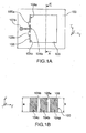
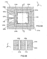
- FIG. 1A-1B A first example of an interconnection structure is given on the Figures 1A-1B (the Figure 1A representing the structure in a view from above while the Figure 1B illustrates this structure in a cross-sectional view, the sectional plane being indicated on the Figure 1A ).
- the structure is made in a support 100 which may be for example in the form of a layer, or a stack of several layers, or a substrate, or a stack of several substrates, or an interposer, and has a cavity 103 passing through the thickness of the support between its upper face (shown in FIG. Figure 1A ) and its underside.
- a support 100 which may be for example in the form of a layer, or a stack of several layers, or a substrate, or a stack of several substrates, or an interposer, and has a cavity 103 passing through the thickness of the support between its upper face (shown in FIG. Figure 1A ) and its underside.
- the support 100 may be for example of semiconductor material, or of insulating material, for example glass.
- the interconnection structure makes it possible to connect elements or devices located on either side of the lower face and the upper face of the support.
- the interconnection structure may possibly be made in a central zone of the support.
- a vertical wall of the cavity 103 is covered with elements 104a, 104b, 104c, based on a conductive material 106 such as for example copper, aluminum, or tungsten or polysilicon.
- a conductive material 106 such as for example copper, aluminum, or tungsten or polysilicon.
- the conductive elements 104a and 104b may be in the form of plates lining a vertical wall of the cavity 103 (the vertical direction being defined as a direction parallel to the vector k orthogonal reference [O; i ; j ; k ] given on the figures).
- the conductive elements 104a, 104b are separated from each other by a groove 105a communicating with the cavity 103 and formed at said vertical wall, while another groove 105b separates the conductive elements 104b and 104c. These grooves 105a, 105b extend in the vertical direction and pass through the thickness e of the support 100 which, in this example, corresponds to the height h of the cavity 103.
- the grooves 105a, 105b and the cavity 103 communicating with the latter form a hole whose vertical walls form a closed contour.
- the grooves 105a, 105b and the cavity 103 may have been made simultaneously or successively, for example by etching such as a DRIE (DRIE for "Deep reactive ion etching") etching or a laser etching.
- etching such as a DRIE (DRIE for "Deep reactive ion etching") etching or a laser etching.
- the grooves 105a, 105b make it possible to provide an electrical discontinuity between the conducting elements 104a, 104b, 104c.
- the conductive elements 104a, 104b, 104c are not connected to each other or electrically connected to each other.
- one of the conductive elements 104b is extended by a conductive track 107b which extends on the upper face of the support 100 parallel to the main plane of the latter (the main plane of the support being defined as a plane passing through the latter and parallel to the plane [O; i ; j ] given on the figures).
- the conductive elements 104a, 104b, 104c can be extended respectively by conductive tracks 107a, 107b, 107c, which extend on the upper face of the support 100.
- vertical connecting elements 114a, 114b made of conducting material in the form of conductive lines are furthermore arranged in the grooves 105a, 105b, and pass through the thickness of the support 100.
- the elements 114a, 114b, just as the grooves 105a, 105b produce a non-zero angle with respect to the main plane of the support, and are, in this example, perpendicular to the main plane of the support.
- connection elements 114a, 114b cover only a portion of the walls of the grooves 105a, 105b.
- connection elements 114a, 114b are respectively extended by conducting tracks 117a, 117b, which extend on the upper face of the support 100.
- the structure comprises conducting elements 104a, 104b, 104c on a wall of the cavity 103 and connecting elements 114a, 114b in the grooves, the connecting elements 114a, 114b in the grooves are connected to conductive tracks 117a, 117b , which extend on the upper face of the support, while the conductive element 104b is also connected to a track 107b resting on the support.
- connection elements 114a, 114b cover only a portion of the grooves 105a, 105b, the latter making it possible to provide an electrical discontinuity between the connecting elements 114a, 114b and the conducting elements 104a, 104b, 104c.
- the grooves 105a, 105b make it possible to separate and electrically isolate the connection elements 104a, 104b, 104c from the conductive elements 114a, 114b.
- the conductive elements 104a, 104c are furthermore connected respectively to the conductive tracks 107a, 107c disposed on the upper face of the support 100.
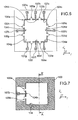
- FIG. 1 An example of a structure with a cavity 103 whose vertical walls are each covered with conducting elements, the conductive elements 104a, 104b, 104c, 104d, 104e, 104f, 104g, 104h being separated by a succession of grooves 105a, 105b, 105c , 105d, 105e, 105f, 105g, 105h, formed all around the cavity 103 is given figure 6 .
- FIG. figure 7 Another example of an interconnection structure formed in a cavity 103 is illustrated in FIG. figure 7 .
- the vertical walls of the cavity 103 are entirely lined by a conductive zone 114, which also covers part of the upper face of the support 100.
- a connecting member 104b formed on a vertical wall of the cavity 103 is separated and disconnected from the conductive zone 114 via the vertical grooves 105a, 105b communicating with the cavity 103.
- connection element 104b is extended by a conductive track 107b which extends on the upper face of the support 100.
- an interconnection structure according to the invention can be made in a cavity 203 formed of several parts 203a, 203b of different dimensions in the thickness of a support 200.
- the cavity or cavities 203 may or may be formed of a first portion 203a, having given dimensions and a second portion 203b located in the extension of the first portion, the second portion part 203b having in a plane parallel to the support, smaller dimensions than the first portion 203a, the first portion 203a and the second portion 203b being delimited by walls forming a staircase profile.
- the stair configuration may allow for example to accommodate a lens in the first portion 203a and position it relative to an imager using the second portion 203b while allowing a rise of electrical contacts along the cavity stairs .
- a staircase profile having a number of steps greater than 2 can be implemented.
- the support 200 may optionally be formed of several layers or of several stacked substrates, for example two layers 200a, 200b or two substrates 200a, 200b, which may be assembled for example by gluing.
- a bead 211 of adhesive may for example be provided between the two substrates 200a, 200b.
- This bead 211 of adhesive may be, according to a first case, formed so as to reach the cavity 203 ( figure 20 ) or so as to be set back from the walls of the cavity 203 ( figure 21 ).
- the first substrate 200a comprises grooves 205a, 205b, vertical communicating with the first portion 203a of the cavity 203 and formed in a wall of this first portion 200a, while the second substrate 200b has vertical grooves 215a, 215b communicating with the second part 203b of the cavity 203 and formed in a wall of this second portion 203b.
- a first conductive zone 214 covers a portion of the upper face of the first substrate 200a, a portion of the vertical walls of the first portion 203a of the cavity 203, a portion of the upper face of the second substrate 200b located at the bottom of the this first portion 203a, and a portion of the vertical walls of the second portion 203b of the cavity 203.
- a second conductive zone 216 is formed of a conductive strip 207b extending on the upper face of the first substrate 200a, extended in a portion covering a vertical wall of the first portion 203a of the cavity , a portion of the upper face of the second substrate 200b located at the bottom of this first portion 203a, and a portion of the vertical walls of the second portion 203b of the cavity 203.
- the first conductive zone 214 and the second conductive zone 216 are separated and electrically insulated from one another via vertical grooves 205a, 205b formed in the first substrate 200a, horizontal trenches 208a, 208b (the horizontal direction being defined as a direction parallel to the plane [O; i ; j ] of the orthogonal reference [O; i ; j ; k ] given on the figures) formed on the second substrate 200b and communicating with the grooves 205a, 205b, and vertical grooves 215a, 215b formed in the second substrate 200b.
- the grooves 205a, 205b, 215a, 215b communicate with the cavity.
- conductive areas 218a, 218b extend along the trenches and have conductive areas extending along the trenches.
- the trenches 208a, 208b may be formed so that their mouth is narrower than their bottom.
- zones 218a, 218b can indeed be made by metal deposition, the metal being, by shading effect due to the shape of the trenches 208a, 208b, deposited on a portion of the bottom of the trenches.
- the horizontal trenches 208a, 208b, formed in the second substrate 200b are replaced by zones 206a, 206b of the second substrate 200b which are exposed and are not covered with conductive material.
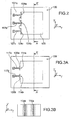
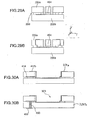
- An interconnection structure with a cavity 303 "blind” can also be provided ( Figures 11A and 11B ).
- the cavity 303 can be formed in the thickness of a first substrate 200a, resting on a second substrate 200b, the cavity 303 traversing the thickness of the first substrate 200a, and having a bottom at the level of the second substrate 200b and which can be formed by the upper face of the latter.
- a portion of the upper face of the first substrate 200a, a part of the walls of the cavity, as well as the upper face of the second substrate 200b are covered by a conductive zone 314.
- a metal track 207b extends on the upper face of the first substrate 200a, on a wall of the cavity 303, and on the upper face of the second substrate 200b.
- This metal track 207b is separated and electrically isolated from the conductive zone 314 via grooves 205a, 205b formed in the walls of the cavity, as well as areas of the substrates 200a, 200b which are not covered with metallic material.
- FIG. 12A-12B Another example of an interconnection structure with a blind cavity is given on the Figures 12A-12B .
- Grooves 205a, 205b, 205c, 205d, 205e, 205f, 205g, 205h are formed around the cavity and electrically isolate between them conductive elements 307a, 307b, 307c, 307d, 307e, 307f, 307g, 307h, formed each of a conductive track extending over the first substrate 200a, an area conductive covering a wall of the cavity, and another conductive track extending at the bottom of the cavity 303 on the second substrate 200b.
- the conductive elements 307a, 307b, 307c, 307d, 307e, 307f, 307g, 307h can be connected to vias 317 passing through the second substrate 200b ( figure 13 ).
- a variant of this structure is given on the figure 14 and provides conductive elements 407h, 407d each formed of a conductive strip extending over the first substrate 200a, a conductive area covering a wall of the cavity, and another conductive strip between the first 200a and the second substrate 200b, this other conductive strip being connected to a via 317.
- interconnection areas 350 formed of metal tracks 351 in a dielectric material layer 352 are provided between the first substrate 200a and the second substrate 200b, and provide a connection between the conductive elements 307h, 307d of the first substrate 200a. and other conductive elements of the second substrate 200b, for example vias 317 passing through the second substrate 200b ( figure 15 ) or metal zones 318 resting on the second substrate 200b ( figure 16 ) or metal zones 319 covering portions of the two faces of the second substrate 200b, as well as walls of an opening passing through the second substrate 200b ( figure 17 ).
- the cavity of the above-described interconnection structure can be formed once the substrates 200a and 200b have been assembled and connected.
- FIGS 19A-19B illustrate an exemplary embodiment of an interconnection structure in which the bottom and the walls of a blind cavity 303 are covered with a metal layer 416 to which metal strips 407a, 407b, 407c, 407d, 407e, 407f, 407g, 407h resting on the first substrate 200a are formed.
- portions of the metal zone 416 are removed at the bottom of the cavity 303.
- the removal may be performed such that the metal layer 416 is withdrawn between grooves facing each other on opposite walls of the cavity 303.
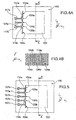
- FIGS. Figures 22A-22C An example of a method for producing a cavity provided with insulation grooves as provided in an interconnection structure according to the invention is illustrated in FIGS. Figures 22A-22C .
- Plates 101a, 101b are first formed in the thickness of a support 100, which may be in the form of a layer or a stack of layers or a substrate ( figure 22A ).
- the pads 101a, 101b may be conductive pads for example based on a metallic material such as copper, aluminum or tungsten or polysilicon. These pads may be vias isolated through a thickness of dielectric material surrounding them.
- a cavity 103 is formed which passes through the support 100.
- the cavity 103 is made to pass through a portion of the support where a portion of the conductive pads 101a, 101b is located, and thus to start and remove a portion of the conductive pads 101a, 101b ( figure 22B ).
- conductive pads 201a, 201b of large size are formed in the support ( Figure 23A ).
- a cavity 103 is formed through the support 100 and an area where the conductive pads 201a, 201b are located, and so as to start and remove a large portion of the latter and to keep another portion against a flank of the cavity 103 ( Figure 23B ).
- an insulating layer (not shown) may be previously deposited on the vertical walls of the cavity.
- Grooves 105a, 105b are then formed at at least one vertical wall of the cavity, the grooves 105a, 105b communicating with cavity 103.
- the grooves 105a, 105b are made to remove portions of the area 108 of conductive material.
- a first conducting zone 108a lining a part of the walls of the cavity 103 is separated from a second conducting zone 108b covering a part of a wall of the cavity 103, via the grooves 105a, 105b ( figure 24B ).
- the cavity 103 and the grooves 105a, 105b are formed in a support 100 at the same time or consecutively ( figure 25A ).
- a layer of sacrificial material 109 is deposited in the grooves 105a, 105b or on the walls of the grooves 105a, 105b, the sacrificial material 109 being distributed so as to form a separation between the cavity 103 and the grooves 105a, 105b ( figure 25B ).
- the sacrificial material layer 109 may be provided to protrude into the cavity 103.
- the sacrificial material 109 may be, for example, SiO 2 or Si 3 N 4 .
- a conductive material layer 108 is deposited so as to line the walls of the cavity 103 and cover the sacrificial material 109.
- the conductive material may be deposited for example by PVD (PVD for "Physical Vapor Deposition”).
- the thickness of the conductive material layer 108 may be less than the thickness of the sacrificial material layer 109 protruding into the cavity 103 ( figure 25C ).
- the layer of sacrificial material 109 is then removed, resulting in a withdrawal of the conductive material 108 facing the grooves 105a, 105b for example by wet chemical etching.
- the conductive area 108 is in the form of two distinct conducting portions 108a and 108b which are not connected to each other and are separated by means of the grooves 105a, 105b ( figure 25D ).
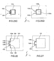
- a cavity 103 passing through the support 100 and at least one vertical groove 105 extending in the thickness of the support 100 and communicating with the cavity 103 are made in a support 100.
- the groove may have for example a rectangular section ( figure 26 ) or oval ( figure 27 ).
- Parts 106a, 106b of a wall 104 of the cavity 103 form a separation between the latter and the groove 105.
- a metallic deposit 108 is then made so as to cover a wall of the cavity and on a portion of the groove 105.
- the portions 106a, 106b prevent metal deposition all around the groove so that the metal deposition on the wall 104 of the cavity and on the groove 105, forms a discontinuous zone.
- the metal deposition may be a so-called "directional" deposit in which the material is deposited at a predetermined angle with respect to a normal to the main plane of the support (the main plane of the support being a plane passing through the latter and parallel to the plane [O; i ; j ] of the orthogonal reference [O; i ; j ; k ] given on the figures).
- the parts 106a, 106b prevent a deposit of metal on the periphery of the groove.
- connection element 104b along the groove, which is disconnected from conducting elements 104a and 104c formed on said wall during metal deposition.
- Each of the above methods can be performed for several substrates or multiple layers which are then assembled. During the assembly step, the cavities obtained in the different substrates or the different layers are aligned to obtain the final cavity having the desired shape. This is particularly the case when several cavities of different sections are superimposed, as for the examples described above in connection with the Figures 8A-C , 9A , 9B , 10A, 10B etc.
- FIG. 28A-28B Another example of a method for producing an interconnection structure is given on the Figures 28A-28B , and 29A-29B (the Figures 28A-28B giving a view from above, while the Figures 29A-29B give a cross-sectional view whose cutting plane is indicated on the Figures 28A-28B ).
- the interconnection structure can be made from a support 200 which can optionally be formed of several layers or of several stacked substrates, for example two layers 200a, 200b or two substrates 200a, 200b, which can be assembled by example by gluing with a bead of glue 211.
- a cavity 303 in the form of a blind hole is provided in the first substrate 200a.
- Grooves 105a, 105b, vertical, that is to say orthogonal to the main plane of the support 200 have been formed at a wall of the cavity and communicate with the latter. Portions of the adhesive bead 211 are exposed by the cavity 303.
- the first substrate 200a comprises at least one metal track 404 on its rear face, that is to say the face opposite the second substrate 200b ( Figures 28A and 29A ).
- a deposit of sacrificial material is then carried out in the grooves 105a, 105b and then a deposit of metal material 414 in the cavity 303 and on the support 200.
- the sacrificial material is then removed, and patterns are then formed in the metallic material, for example a metal zone 415 covering walls of the cavity 303, connected to a metal track 417a on the upper face of the support.
- This step also leads to the formation of another metal zone 416 separated from the metal zone 415 via the grooves 105a, 105b, the metal zone 415 covers a wall portion of the cavity located between the grooves 105a, 105b which is extended by another metal track 417b formed on the upper face of the support ( Figures 28B and 29B ).
- the newly formed cavity interconnect structure may be integrated or assembled with another device.
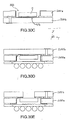
- This process can be carried out from the previously formed structure (and described in connection with the figure 30A representing the device of the figure 28B in a sectional view C'C).
- One or more vias 430 are then formed through the second support 200b and one or more connection pads 432 on this support 200b, the studs 432 being connected to the vias 430 ( figure 30B ).
- An optical component C for example a fixed-focus lens, a parallel-sided blade or a variable-focus device, is then placed in the cavity 303 and connected to the conductive zone 415 formed in this cavity ( figure 30C ).
- an imaging substrate is transferred to the upper face of the first substrate 200a, the imaging substrate being assembled and connected to the metal tracks 417a, 417b formed on the upper face of the first substrate 200a ( figure 30D ).
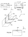
- a cavity interconnection structure as implemented according to the invention can find applications in the field of MEMS components, for example such as inertial sensors, accelerometer or gyrometer ( figure 31 ).
- the figure 32 shows an exemplary unitary camera consisting of an active optical element 500 disposed on the top of the cavity 303, focused on the imaging substrate.
- Contact lifts are implemented in a cavity 303 to supply this active optical element.
Landscapes
- Engineering & Computer Science (AREA)
- Microelectronics & Electronic Packaging (AREA)
- Computer Hardware Design (AREA)
- Manufacturing & Machinery (AREA)
- Micromachines (AREA)
Claims (5)
- Verbindungseinrichtung, umfassend einen Träger (100, 200), in den wenigstens ein Loch eingebracht ist, wobei das Loch Wände aufweist, die eine geschlossene Kontur bilden und wobei es aus einer Kavität (103, 203, 303) und einer oder mehreren Rillen (1 05a-1 05h, 205a-205h, 215a-215b) gebildet ist, die mit der Kavität in Verbindung steht bzw. stehen, wobei die Rillen sich ganz oder teilweise entlang dem Loch erstrecken, ein oder mehrere Leiterelemente (104a-104h, 114a-114b, 214, 314), die dazu bestimmt sind, leitende Bereiche, die sich auf der einen und der anderen Seite von dem Träger befinden miteinander zu verbinden, dadurch gekennzeichnet, dass die Leiterelemente wenigstens einen Teil der Wände der Kavität und nur einen Abschnitt der Rillen (104b) bedecken, wobei die Rillen eine elektrische Diskontinuität (106a, 106b) zwischen den Verbindungselementen in den Rillen (104b) und den Leiterelementen (1 04a) der Kavität sicherstellen.
- Verbindungseinrichtung nach dem vorhergehenden Anspruch, wobei die Kavität (103, 203) die Dicke des Trägers (100, 200) durchquert.
- Verbindungseinrichtung nach Anspruch 1 oder 2, wobei die Kavität (303) aus einem in dem Träger (200) gebildeten Sackloch gebildet ist.
- Verbindungseinrichtung nach einem der Ansprüche 1 bis 3, wobei die Wände der Kavität mit einem leitenden Material bedeckt sind.
- Verfahren zur Herstellung einer Verbindungseinrichtung nach an Anspruch 1 bis 4, umfassend die Schritte:- Bilden einer Kavität in der Dicke des Trägers,- Bilden von wenigstens einer Rille, die mit der Kavität in Verbindung steht und sich über die Gesamtheit oder einen Teil davon erstreckt, wobei die Rille so ausgeführt ist, dass sie, in einer Ebene parallel zu dem Träger einen variablen Querschnitt aufweist, mit einer Verengung auf Höhe der Verbindung zwischen der Rille und der Kavität,- Ausführen einer gerichteten Beschichtung mit einem leitenden Material auf der Wand und auf einem Teil der Rille.
Applications Claiming Priority (1)
| Application Number | Priority Date | Filing Date | Title |
|---|---|---|---|
| FR0957588A FR2951870B1 (fr) | 2009-10-28 | 2009-10-28 | Structure d'interconnexion a cavite presentant une ou plusieurs remontees de contact sur les parois de la cavite et procede de realisation |
Publications (2)
| Publication Number | Publication Date |
|---|---|
| EP2316784A1 EP2316784A1 (de) | 2011-05-04 |
| EP2316784B1 true EP2316784B1 (de) | 2014-02-26 |
Family
ID=42269452
Family Applications (2)
| Application Number | Title | Priority Date | Filing Date |
|---|---|---|---|
| EP10189290A Not-in-force EP2316785B1 (de) | 2009-10-28 | 2010-10-28 | Hohlraumverbindungsstruktur, die eine oder mehrere aufsteigende Leiter an den Wänden des Hohlraums aufweist und deren Herstellungsverfahren |
| EP10189285.9A Not-in-force EP2316784B1 (de) | 2009-10-28 | 2010-10-28 | Hohlraumverbindungsstruktur, die einen oder mehrere aufsteigende Leiter an den Wänden des Hohlraums aufweist, und entsprechendes Herstellungsverfahren |
Family Applications Before (1)
| Application Number | Title | Priority Date | Filing Date |
|---|---|---|---|
| EP10189290A Not-in-force EP2316785B1 (de) | 2009-10-28 | 2010-10-28 | Hohlraumverbindungsstruktur, die eine oder mehrere aufsteigende Leiter an den Wänden des Hohlraums aufweist und deren Herstellungsverfahren |
Country Status (4)
| Country | Link |
|---|---|
| US (1) | US8674489B2 (de) |
| EP (2) | EP2316785B1 (de) |
| JP (1) | JP2011097059A (de) |
| FR (1) | FR2951870B1 (de) |
Families Citing this family (11)
| Publication number | Priority date | Publication date | Assignee | Title |
|---|---|---|---|---|
| FR2931587B1 (fr) * | 2008-05-21 | 2011-05-13 | Commissariat Energie Atomique | Procede de realisation d'un dispositif optique a composants optoelectroniques integres |
| FR2950154B1 (fr) | 2009-09-15 | 2011-12-23 | Commissariat Energie Atomique | Dispositif optique a membrane deformable a actionnement piezoelectrique en forme de couronne continue |
| FR2950153B1 (fr) | 2009-09-15 | 2011-12-23 | Commissariat Energie Atomique | Dispositif optique a membrane deformable a actionnement piezoelectrique |
| FR2957480B1 (fr) * | 2010-03-10 | 2012-08-31 | Commissariat Energie Atomique | Procede de metallisation de vias borgnes |
| US8936967B2 (en) * | 2011-03-23 | 2015-01-20 | Intel Corporation | Solder in cavity interconnection structures |
| CN103895116A (zh) * | 2014-03-28 | 2014-07-02 | 高佳太阳能股份有限公司 | 一种连接板提取工装 |
| US9603255B2 (en) | 2015-02-20 | 2017-03-21 | Nextgin Technology Bv | Method for producing a printed circuit board |
| FR3044165B1 (fr) | 2015-11-23 | 2018-03-16 | Commissariat A L'energie Atomique Et Aux Energies Alternatives | Realisation d'interconnexions par recourbement d'elements conducteurs sous un dispositif microelectronique tel qu'une puce |
| EP3501241A4 (de) | 2016-08-19 | 2020-08-12 | Nextgin Technology B.v. | Verfahren zur herstellung einer druckleiterplatte |
| US11234325B2 (en) | 2019-06-20 | 2022-01-25 | Infinera Corporation | Printed circuit board having a differential pair routing topology with negative plane routing and impedance correction structures |
| CN114679848B (zh) * | 2022-04-19 | 2023-07-11 | 科惠白井(佛冈)电路有限公司 | Pcb板不完全电镀槽的成型方法及pcb板制备方法 |
Family Cites Families (9)
| Publication number | Priority date | Publication date | Assignee | Title |
|---|---|---|---|---|
| US5825084A (en) * | 1996-08-22 | 1998-10-20 | Express Packaging Systems, Inc. | Single-core two-side substrate with u-strip and co-planar signal traces, and power and ground planes through split-wrap-around (SWA) or split-via-connections (SVC) for packaging IC devices |
| JP3629902B2 (ja) * | 1997-06-30 | 2005-03-16 | 沖電気工業株式会社 | 半導体素子の配線構造およびその製造方法 |
| US6137064A (en) * | 1999-06-11 | 2000-10-24 | Teradyne, Inc. | Split via surface mount connector and related techniques |
| FR2802706B1 (fr) * | 1999-12-15 | 2002-03-01 | 3D Plus Sa | Procede et dispositif d'interconnexion en trois dimensions de composants electroniques |
| US6759309B2 (en) * | 2002-05-28 | 2004-07-06 | Applied Materials, Inc. | Micromachined structures including glass vias with internal conductive layers anodically bonded to silicon-containing substrates |
| US6891272B1 (en) * | 2002-07-31 | 2005-05-10 | Silicon Pipe, Inc. | Multi-path via interconnection structures and methods for manufacturing the same |
| TWI249978B (en) * | 2004-05-11 | 2006-02-21 | Via Tech Inc | Circuit substrate and manufacturing method of plated through slot thereof |
| US7204018B2 (en) * | 2004-12-16 | 2007-04-17 | Nortel Networks Limited | Technique for reducing via capacitance |
| FR2931587B1 (fr) | 2008-05-21 | 2011-05-13 | Commissariat Energie Atomique | Procede de realisation d'un dispositif optique a composants optoelectroniques integres |
-
2009
- 2009-10-28 FR FR0957588A patent/FR2951870B1/fr not_active Expired - Fee Related
-
2010
- 2010-10-26 US US12/912,203 patent/US8674489B2/en not_active Expired - Fee Related
- 2010-10-27 JP JP2010240640A patent/JP2011097059A/ja active Pending
- 2010-10-28 EP EP10189290A patent/EP2316785B1/de not_active Not-in-force
- 2010-10-28 EP EP10189285.9A patent/EP2316784B1/de not_active Not-in-force
Also Published As
| Publication number | Publication date |
|---|---|
| US8674489B2 (en) | 2014-03-18 |
| US20110097909A1 (en) | 2011-04-28 |
| EP2316785B1 (de) | 2013-01-09 |
| JP2011097059A (ja) | 2011-05-12 |
| EP2316785A1 (de) | 2011-05-04 |
| FR2951870B1 (fr) | 2012-03-30 |
| EP2316784A1 (de) | 2011-05-04 |
| FR2951870A1 (fr) | 2011-04-29 |
Similar Documents
| Publication | Publication Date | Title |
|---|---|---|
| EP2316784B1 (de) | Hohlraumverbindungsstruktur, die einen oder mehrere aufsteigende Leiter an den Wänden des Hohlraums aufweist, und entsprechendes Herstellungsverfahren | |
| EP0565391B1 (de) | Verfahren und Vorrichtung zur Verkapselung von dreidimensionalen Halbleiterplättchen | |
| EP1966825B1 (de) | Verfahren zur gemeinsamen herstellung von elektronischen 3d-modulen | |
| EP2546188B1 (de) | Verfahren zur Herstellung einer Struktur mit einer aufgehängten Membran und einer vergrabenen Elektrode | |
| EP4092730A2 (de) | Herstellung von elektronischen chips | |
| FR2992467A1 (fr) | Procede de realisation d'un composant a contact electrique traversant et composant obtenu | |
| FR2847385A1 (fr) | Substrat multicouche en ceramique et procede de fabrication de celui-ci | |
| EP2963695A2 (de) | Elektrische mehrschichtenvorrichtung | |
| EP2772943B1 (de) | Herstellungsverfahren einer mikroelektronischen Vorrichtung und entsprechende Vorrichtung | |
| EP3136428B1 (de) | Chip zum montieren auf der oberfläche | |
| EP3494594B1 (de) | Herstellungsverfahren eines dreidimensionalen leistungsmoduls | |
| EP3157057B1 (de) | Gehäuse für mikroelektronische bauteile | |
| EP2339616B1 (de) | Vereinfachtes Herstellungsverfahren eines Hybridsubstrats | |
| EP2383775B1 (de) | Method for obtaining a layer of AlN with substantially vertical flanks | |
| EP2161238B1 (de) | Dreidimensionale Struktur mit sehr hoher Dichte | |
| EP0338063B1 (de) | Aufzeichnungs-wiedergabemagnetkopf und verfahren zu seiner herstellung | |
| EP3171395B1 (de) | Herstellung von verbindungen durch umbiegen von leiterelementen unter eine mikroelektronische vorrichtung wie einen chip | |
| FR2738705A1 (fr) | Dispositif capteur electromecanique et procede de fabrication d'un tel dispositif | |
| FR2917231A1 (fr) | Realisation de condensateurs dotes de moyens pour diminuer les contraintes du materiau metallique de son armature inferieure | |
| FR2978296A1 (fr) | Puce electronique comportant des piliers de connexion, et procede de fabrication | |
| FR3009649A1 (fr) | Interconnexion de plusieurs niveaux d'un empilement de supports de composants electroniques | |
| FR3012671A1 (fr) | Dispositif mecanique integre a mouvement vertical | |
| EP2498287A2 (de) | Verfahren zur Herstellung von vertikalen Verbindungen durch strukturierte Schichten hindurch | |
| EP3467856B1 (de) | Herstellungsverfahren einer hermetischen und isolierenden durchführung für ein gehäuse, insbesondere aus titan, einer elektronischen vorrichtung | |
| EP4593074A1 (de) | Elektronisches bauelement mit anschlusssäulen |
Legal Events
| Date | Code | Title | Description |
|---|---|---|---|
| PUAI | Public reference made under article 153(3) epc to a published international application that has entered the european phase |
Free format text: ORIGINAL CODE: 0009012 |
|
| AK | Designated contracting states |
Kind code of ref document: A1 Designated state(s): AL AT BE BG CH CY CZ DE DK EE ES FI FR GB GR HR HU IE IS IT LI LT LU LV MC MK MT NL NO PL PT RO RS SE SI SK SM TR |
|
| AX | Request for extension of the european patent |
Extension state: BA ME |
|
| 17P | Request for examination filed |
Effective date: 20110909 |
|
| 17Q | First examination report despatched |
Effective date: 20120116 |
|
| GRAP | Despatch of communication of intention to grant a patent |
Free format text: ORIGINAL CODE: EPIDOSNIGR1 |
|
| INTG | Intention to grant announced |
Effective date: 20130419 |
|
| GRAP | Despatch of communication of intention to grant a patent |
Free format text: ORIGINAL CODE: EPIDOSNIGR1 |
|
| RIC1 | Information provided on ipc code assigned before grant |
Ipc: B81B 7/00 20060101AFI20130815BHEP Ipc: H05K 3/40 20060101ALI20130815BHEP Ipc: H01L 27/146 20060101ALN20130815BHEP Ipc: H01L 23/538 20060101ALN20130815BHEP Ipc: H05K 1/18 20060101ALN20130815BHEP Ipc: H05K 1/02 20060101ALN20130815BHEP Ipc: H01L 23/48 20060101ALI20130815BHEP Ipc: H05K 3/46 20060101ALN20130815BHEP |
|
| RIC1 | Information provided on ipc code assigned before grant |
Ipc: H05K 3/46 20060101ALN20130827BHEP Ipc: B81B 7/00 20060101AFI20130827BHEP Ipc: H01L 23/538 20060101ALN20130827BHEP Ipc: H05K 3/40 20060101ALI20130827BHEP Ipc: H05K 1/18 20060101ALN20130827BHEP Ipc: H01L 27/146 20060101ALN20130827BHEP Ipc: H05K 1/02 20060101ALN20130827BHEP Ipc: H01L 23/48 20060101ALI20130827BHEP |
|
| INTG | Intention to grant announced |
Effective date: 20130912 |
|
| GRAS | Grant fee paid |
Free format text: ORIGINAL CODE: EPIDOSNIGR3 |
|
| GRAA | (expected) grant |
Free format text: ORIGINAL CODE: 0009210 |
|
| AK | Designated contracting states |
Kind code of ref document: B1 Designated state(s): AL AT BE BG CH CY CZ DE DK EE ES FI FR GB GR HR HU IE IS IT LI LT LU LV MC MK MT NL NO PL PT RO RS SE SI SK SM TR |
|
| REG | Reference to a national code |
Ref country code: GB Ref legal event code: FG4D Free format text: NOT ENGLISH |
|
| REG | Reference to a national code |
Ref country code: CH Ref legal event code: EP |
|
| REG | Reference to a national code |
Ref country code: AT Ref legal event code: REF Ref document number: 653478 Country of ref document: AT Kind code of ref document: T Effective date: 20140315 |
|
| REG | Reference to a national code |
Ref country code: IE Ref legal event code: FG4D Free format text: LANGUAGE OF EP DOCUMENT: FRENCH |
|
| REG | Reference to a national code |
Ref country code: DE Ref legal event code: R096 Ref document number: 602010013702 Country of ref document: DE Effective date: 20140410 |
|
| REG | Reference to a national code |
Ref country code: NL Ref legal event code: VDEP Effective date: 20140226 |
|
| REG | Reference to a national code |
Ref country code: AT Ref legal event code: MK05 Ref document number: 653478 Country of ref document: AT Kind code of ref document: T Effective date: 20140226 |
|
| REG | Reference to a national code |
Ref country code: LT Ref legal event code: MG4D |
|
| PG25 | Lapsed in a contracting state [announced via postgrant information from national office to epo] |
Ref country code: NO Free format text: LAPSE BECAUSE OF FAILURE TO SUBMIT A TRANSLATION OF THE DESCRIPTION OR TO PAY THE FEE WITHIN THE PRESCRIBED TIME-LIMIT Effective date: 20140526 Ref country code: IS Free format text: LAPSE BECAUSE OF FAILURE TO SUBMIT A TRANSLATION OF THE DESCRIPTION OR TO PAY THE FEE WITHIN THE PRESCRIBED TIME-LIMIT Effective date: 20140626 Ref country code: LT Free format text: LAPSE BECAUSE OF FAILURE TO SUBMIT A TRANSLATION OF THE DESCRIPTION OR TO PAY THE FEE WITHIN THE PRESCRIBED TIME-LIMIT Effective date: 20140226 |
|
| PG25 | Lapsed in a contracting state [announced via postgrant information from national office to epo] |
Ref country code: CY Free format text: LAPSE BECAUSE OF FAILURE TO SUBMIT A TRANSLATION OF THE DESCRIPTION OR TO PAY THE FEE WITHIN THE PRESCRIBED TIME-LIMIT Effective date: 20140226 Ref country code: SE Free format text: LAPSE BECAUSE OF FAILURE TO SUBMIT A TRANSLATION OF THE DESCRIPTION OR TO PAY THE FEE WITHIN THE PRESCRIBED TIME-LIMIT Effective date: 20140226 Ref country code: FI Free format text: LAPSE BECAUSE OF FAILURE TO SUBMIT A TRANSLATION OF THE DESCRIPTION OR TO PAY THE FEE WITHIN THE PRESCRIBED TIME-LIMIT Effective date: 20140226 Ref country code: PT Free format text: LAPSE BECAUSE OF FAILURE TO SUBMIT A TRANSLATION OF THE DESCRIPTION OR TO PAY THE FEE WITHIN THE PRESCRIBED TIME-LIMIT Effective date: 20140626 Ref country code: NL Free format text: LAPSE BECAUSE OF FAILURE TO SUBMIT A TRANSLATION OF THE DESCRIPTION OR TO PAY THE FEE WITHIN THE PRESCRIBED TIME-LIMIT Effective date: 20140226 Ref country code: AT Free format text: LAPSE BECAUSE OF FAILURE TO SUBMIT A TRANSLATION OF THE DESCRIPTION OR TO PAY THE FEE WITHIN THE PRESCRIBED TIME-LIMIT Effective date: 20140226 |
|
| PG25 | Lapsed in a contracting state [announced via postgrant information from national office to epo] |
Ref country code: RS Free format text: LAPSE BECAUSE OF FAILURE TO SUBMIT A TRANSLATION OF THE DESCRIPTION OR TO PAY THE FEE WITHIN THE PRESCRIBED TIME-LIMIT Effective date: 20140226 Ref country code: LV Free format text: LAPSE BECAUSE OF FAILURE TO SUBMIT A TRANSLATION OF THE DESCRIPTION OR TO PAY THE FEE WITHIN THE PRESCRIBED TIME-LIMIT Effective date: 20140226 Ref country code: HR Free format text: LAPSE BECAUSE OF FAILURE TO SUBMIT A TRANSLATION OF THE DESCRIPTION OR TO PAY THE FEE WITHIN THE PRESCRIBED TIME-LIMIT Effective date: 20140226 |
|
| PG25 | Lapsed in a contracting state [announced via postgrant information from national office to epo] |
Ref country code: CZ Free format text: LAPSE BECAUSE OF FAILURE TO SUBMIT A TRANSLATION OF THE DESCRIPTION OR TO PAY THE FEE WITHIN THE PRESCRIBED TIME-LIMIT Effective date: 20140226 Ref country code: DK Free format text: LAPSE BECAUSE OF FAILURE TO SUBMIT A TRANSLATION OF THE DESCRIPTION OR TO PAY THE FEE WITHIN THE PRESCRIBED TIME-LIMIT Effective date: 20140226 Ref country code: EE Free format text: LAPSE BECAUSE OF FAILURE TO SUBMIT A TRANSLATION OF THE DESCRIPTION OR TO PAY THE FEE WITHIN THE PRESCRIBED TIME-LIMIT Effective date: 20140226 Ref country code: RO Free format text: LAPSE BECAUSE OF FAILURE TO SUBMIT A TRANSLATION OF THE DESCRIPTION OR TO PAY THE FEE WITHIN THE PRESCRIBED TIME-LIMIT Effective date: 20140226 |
|
| REG | Reference to a national code |
Ref country code: DE Ref legal event code: R097 Ref document number: 602010013702 Country of ref document: DE |
|
| PG25 | Lapsed in a contracting state [announced via postgrant information from national office to epo] |
Ref country code: PL Free format text: LAPSE BECAUSE OF FAILURE TO SUBMIT A TRANSLATION OF THE DESCRIPTION OR TO PAY THE FEE WITHIN THE PRESCRIBED TIME-LIMIT Effective date: 20140226 Ref country code: SK Free format text: LAPSE BECAUSE OF FAILURE TO SUBMIT A TRANSLATION OF THE DESCRIPTION OR TO PAY THE FEE WITHIN THE PRESCRIBED TIME-LIMIT Effective date: 20140226 Ref country code: ES Free format text: LAPSE BECAUSE OF FAILURE TO SUBMIT A TRANSLATION OF THE DESCRIPTION OR TO PAY THE FEE WITHIN THE PRESCRIBED TIME-LIMIT Effective date: 20140226 |
|
| PLBE | No opposition filed within time limit |
Free format text: ORIGINAL CODE: 0009261 |
|
| STAA | Information on the status of an ep patent application or granted ep patent |
Free format text: STATUS: NO OPPOSITION FILED WITHIN TIME LIMIT |
|
| 26N | No opposition filed |
Effective date: 20141127 |
|
| REG | Reference to a national code |
Ref country code: DE Ref legal event code: R097 Ref document number: 602010013702 Country of ref document: DE Effective date: 20141127 |
|
| PG25 | Lapsed in a contracting state [announced via postgrant information from national office to epo] |
Ref country code: IT Free format text: LAPSE BECAUSE OF FAILURE TO SUBMIT A TRANSLATION OF THE DESCRIPTION OR TO PAY THE FEE WITHIN THE PRESCRIBED TIME-LIMIT Effective date: 20140226 |
|
| PG25 | Lapsed in a contracting state [announced via postgrant information from national office to epo] |
Ref country code: MC Free format text: LAPSE BECAUSE OF FAILURE TO SUBMIT A TRANSLATION OF THE DESCRIPTION OR TO PAY THE FEE WITHIN THE PRESCRIBED TIME-LIMIT Effective date: 20140226 Ref country code: SI Free format text: LAPSE BECAUSE OF FAILURE TO SUBMIT A TRANSLATION OF THE DESCRIPTION OR TO PAY THE FEE WITHIN THE PRESCRIBED TIME-LIMIT Effective date: 20140226 Ref country code: LU Free format text: LAPSE BECAUSE OF FAILURE TO SUBMIT A TRANSLATION OF THE DESCRIPTION OR TO PAY THE FEE WITHIN THE PRESCRIBED TIME-LIMIT Effective date: 20141028 |
|
| REG | Reference to a national code |
Ref country code: CH Ref legal event code: PL |
|
| PG25 | Lapsed in a contracting state [announced via postgrant information from national office to epo] |
Ref country code: BE Free format text: LAPSE BECAUSE OF NON-PAYMENT OF DUE FEES Effective date: 20141031 |
|
| REG | Reference to a national code |
Ref country code: IE Ref legal event code: MM4A |
|
| PG25 | Lapsed in a contracting state [announced via postgrant information from national office to epo] |
Ref country code: CH Free format text: LAPSE BECAUSE OF NON-PAYMENT OF DUE FEES Effective date: 20141031 Ref country code: LI Free format text: LAPSE BECAUSE OF NON-PAYMENT OF DUE FEES Effective date: 20141031 |
|
| PG25 | Lapsed in a contracting state [announced via postgrant information from national office to epo] |
Ref country code: IE Free format text: LAPSE BECAUSE OF NON-PAYMENT OF DUE FEES Effective date: 20141028 |
|
| REG | Reference to a national code |
Ref country code: FR Ref legal event code: PLFP Year of fee payment: 6 |
|
| PG25 | Lapsed in a contracting state [announced via postgrant information from national office to epo] |
Ref country code: SM Free format text: LAPSE BECAUSE OF FAILURE TO SUBMIT A TRANSLATION OF THE DESCRIPTION OR TO PAY THE FEE WITHIN THE PRESCRIBED TIME-LIMIT Effective date: 20140226 |
|
| PG25 | Lapsed in a contracting state [announced via postgrant information from national office to epo] |
Ref country code: BG Free format text: LAPSE BECAUSE OF FAILURE TO SUBMIT A TRANSLATION OF THE DESCRIPTION OR TO PAY THE FEE WITHIN THE PRESCRIBED TIME-LIMIT Effective date: 20140226 Ref country code: GR Free format text: LAPSE BECAUSE OF FAILURE TO SUBMIT A TRANSLATION OF THE DESCRIPTION OR TO PAY THE FEE WITHIN THE PRESCRIBED TIME-LIMIT Effective date: 20140527 |
|
| PG25 | Lapsed in a contracting state [announced via postgrant information from national office to epo] |
Ref country code: MT Free format text: LAPSE BECAUSE OF FAILURE TO SUBMIT A TRANSLATION OF THE DESCRIPTION OR TO PAY THE FEE WITHIN THE PRESCRIBED TIME-LIMIT Effective date: 20140226 Ref country code: HU Free format text: LAPSE BECAUSE OF FAILURE TO SUBMIT A TRANSLATION OF THE DESCRIPTION OR TO PAY THE FEE WITHIN THE PRESCRIBED TIME-LIMIT; INVALID AB INITIO Effective date: 20101028 Ref country code: TR Free format text: LAPSE BECAUSE OF FAILURE TO SUBMIT A TRANSLATION OF THE DESCRIPTION OR TO PAY THE FEE WITHIN THE PRESCRIBED TIME-LIMIT Effective date: 20140226 |
|
| REG | Reference to a national code |
Ref country code: FR Ref legal event code: PLFP Year of fee payment: 7 |
|
| REG | Reference to a national code |
Ref country code: FR Ref legal event code: PLFP Year of fee payment: 8 |
|
| PG25 | Lapsed in a contracting state [announced via postgrant information from national office to epo] |
Ref country code: MK Free format text: LAPSE BECAUSE OF FAILURE TO SUBMIT A TRANSLATION OF THE DESCRIPTION OR TO PAY THE FEE WITHIN THE PRESCRIBED TIME-LIMIT Effective date: 20140226 |
|
| REG | Reference to a national code |
Ref country code: FR Ref legal event code: PLFP Year of fee payment: 9 |
|
| PG25 | Lapsed in a contracting state [announced via postgrant information from national office to epo] |
Ref country code: AL Free format text: LAPSE BECAUSE OF FAILURE TO SUBMIT A TRANSLATION OF THE DESCRIPTION OR TO PAY THE FEE WITHIN THE PRESCRIBED TIME-LIMIT Effective date: 20140226 |
|
| PGFP | Annual fee paid to national office [announced via postgrant information from national office to epo] |
Ref country code: FR Payment date: 20221020 Year of fee payment: 13 |
|
| PGFP | Annual fee paid to national office [announced via postgrant information from national office to epo] |
Ref country code: GB Payment date: 20221024 Year of fee payment: 13 Ref country code: DE Payment date: 20221020 Year of fee payment: 13 |
|
| REG | Reference to a national code |
Ref country code: DE Ref legal event code: R119 Ref document number: 602010013702 Country of ref document: DE |
|
| GBPC | Gb: european patent ceased through non-payment of renewal fee |
Effective date: 20231028 |
|
| PG25 | Lapsed in a contracting state [announced via postgrant information from national office to epo] |
Ref country code: GB Free format text: LAPSE BECAUSE OF NON-PAYMENT OF DUE FEES Effective date: 20231028 |
|
| PG25 | Lapsed in a contracting state [announced via postgrant information from national office to epo] |
Ref country code: GB Free format text: LAPSE BECAUSE OF NON-PAYMENT OF DUE FEES Effective date: 20231028 Ref country code: FR Free format text: LAPSE BECAUSE OF NON-PAYMENT OF DUE FEES Effective date: 20231031 Ref country code: DE Free format text: LAPSE BECAUSE OF NON-PAYMENT OF DUE FEES Effective date: 20240501 |