EP2299494A2 - Semiconductor device - Google Patents
Semiconductor device Download PDFInfo
- Publication number
- EP2299494A2 EP2299494A2 EP10009573A EP10009573A EP2299494A2 EP 2299494 A2 EP2299494 A2 EP 2299494A2 EP 10009573 A EP10009573 A EP 10009573A EP 10009573 A EP10009573 A EP 10009573A EP 2299494 A2 EP2299494 A2 EP 2299494A2
- Authority
- EP
- European Patent Office
- Prior art keywords
- semiconductor layer
- conductivity
- type
- transistor
- layer
- Prior art date
- Legal status (The legal status is an assumption and is not a legal conclusion. Google has not performed a legal analysis and makes no representation as to the accuracy of the status listed.)
- Withdrawn
Links
Images





















Classifications
-
- H—ELECTRICITY
- H10—SEMICONDUCTOR DEVICES; ELECTRIC SOLID-STATE DEVICES NOT OTHERWISE PROVIDED FOR
- H10D—INORGANIC ELECTRIC SEMICONDUCTOR DEVICES
- H10D30/00—Field-effect transistors [FET]
- H10D30/60—Insulated-gate field-effect transistors [IGFET]
- H10D30/63—Vertical IGFETs
-
- H—ELECTRICITY
- H10—SEMICONDUCTOR DEVICES; ELECTRIC SOLID-STATE DEVICES NOT OTHERWISE PROVIDED FOR
- H10B—ELECTRONIC MEMORY DEVICES
- H10B10/00—Static random access memory [SRAM] devices
-
- H—ELECTRICITY
- H10—SEMICONDUCTOR DEVICES; ELECTRIC SOLID-STATE DEVICES NOT OTHERWISE PROVIDED FOR
- H10B—ELECTRONIC MEMORY DEVICES
- H10B99/00—Subject matter not provided for in other groups of this subclass
-
- H—ELECTRICITY
- H10—SEMICONDUCTOR DEVICES; ELECTRIC SOLID-STATE DEVICES NOT OTHERWISE PROVIDED FOR
- H10D—INORGANIC ELECTRIC SEMICONDUCTOR DEVICES
- H10D30/00—Field-effect transistors [FET]
- H10D30/60—Insulated-gate field-effect transistors [IGFET]
- H10D30/67—Thin-film transistors [TFT]
- H10D30/6728—Vertical TFTs
-
- H—ELECTRICITY
- H10—SEMICONDUCTOR DEVICES; ELECTRIC SOLID-STATE DEVICES NOT OTHERWISE PROVIDED FOR
- H10D—INORGANIC ELECTRIC SEMICONDUCTOR DEVICES
- H10D84/00—Integrated devices formed in or on semiconductor substrates that comprise only semiconducting layers, e.g. on Si wafers or on GaAs-on-Si wafers
- H10D84/01—Manufacture or treatment
- H10D84/0123—Integrating together multiple components covered by H10D12/00 or H10D30/00, e.g. integrating multiple IGBTs
- H10D84/0126—Integrating together multiple components covered by H10D12/00 or H10D30/00, e.g. integrating multiple IGBTs the components including insulated gates, e.g. IGFETs
- H10D84/0165—Integrating together multiple components covered by H10D12/00 or H10D30/00, e.g. integrating multiple IGBTs the components including insulated gates, e.g. IGFETs the components including complementary IGFETs, e.g. CMOS devices
- H10D84/0195—Integrating together multiple components covered by H10D12/00 or H10D30/00, e.g. integrating multiple IGBTs the components including insulated gates, e.g. IGFETs the components including complementary IGFETs, e.g. CMOS devices the components including vertical IGFETs
-
- H—ELECTRICITY
- H10—SEMICONDUCTOR DEVICES; ELECTRIC SOLID-STATE DEVICES NOT OTHERWISE PROVIDED FOR
- H10D—INORGANIC ELECTRIC SEMICONDUCTOR DEVICES
- H10D84/00—Integrated devices formed in or on semiconductor substrates that comprise only semiconducting layers, e.g. on Si wafers or on GaAs-on-Si wafers
- H10D84/01—Manufacture or treatment
- H10D84/02—Manufacture or treatment characterised by using material-based technologies
- H10D84/03—Manufacture or treatment characterised by using material-based technologies using Group IV technology, e.g. silicon technology or silicon-carbide [SiC] technology
- H10D84/038—Manufacture or treatment characterised by using material-based technologies using Group IV technology, e.g. silicon technology or silicon-carbide [SiC] technology using silicon technology, e.g. SiGe
-
- H—ELECTRICITY
- H10—SEMICONDUCTOR DEVICES; ELECTRIC SOLID-STATE DEVICES NOT OTHERWISE PROVIDED FOR
- H10D—INORGANIC ELECTRIC SEMICONDUCTOR DEVICES
- H10D84/00—Integrated devices formed in or on semiconductor substrates that comprise only semiconducting layers, e.g. on Si wafers or on GaAs-on-Si wafers
- H10D84/80—Integrated devices formed in or on semiconductor substrates that comprise only semiconducting layers, e.g. on Si wafers or on GaAs-on-Si wafers characterised by the integration of at least one component covered by groups H10D12/00 or H10D30/00, e.g. integration of IGFETs
- H10D84/82—Integrated devices formed in or on semiconductor substrates that comprise only semiconducting layers, e.g. on Si wafers or on GaAs-on-Si wafers characterised by the integration of at least one component covered by groups H10D12/00 or H10D30/00, e.g. integration of IGFETs of only field-effect components
- H10D84/83—Integrated devices formed in or on semiconductor substrates that comprise only semiconducting layers, e.g. on Si wafers or on GaAs-on-Si wafers characterised by the integration of at least one component covered by groups H10D12/00 or H10D30/00, e.g. integration of IGFETs of only field-effect components of only insulated-gate FETs [IGFET]
- H10D84/85—Complementary IGFETs, e.g. CMOS
-
- H—ELECTRICITY
- H10—SEMICONDUCTOR DEVICES; ELECTRIC SOLID-STATE DEVICES NOT OTHERWISE PROVIDED FOR
- H10D—INORGANIC ELECTRIC SEMICONDUCTOR DEVICES
- H10D86/00—Integrated devices formed in or on insulating or conducting substrates, e.g. formed in silicon-on-insulator [SOI] substrates or on stainless steel or glass substrates
- H10D86/01—Manufacture or treatment
-
- H—ELECTRICITY
- H10—SEMICONDUCTOR DEVICES; ELECTRIC SOLID-STATE DEVICES NOT OTHERWISE PROVIDED FOR
- H10D—INORGANIC ELECTRIC SEMICONDUCTOR DEVICES
- H10D86/00—Integrated devices formed in or on insulating or conducting substrates, e.g. formed in silicon-on-insulator [SOI] substrates or on stainless steel or glass substrates
- H10D86/201—Integrated devices formed in or on insulating or conducting substrates, e.g. formed in silicon-on-insulator [SOI] substrates or on stainless steel or glass substrates the substrates comprising an insulating layer on a semiconductor body, e.g. SOI
Definitions
- the present invention relates to a semiconductor device.
- MOS transistor which is a field-effect transistor having a gate electrode with a MOS (metal-oxide semiconductor) structure
- MOS metal-oxide semiconductor
- SGT Surrounding Gate Transistor
- CMOS inverter circuits using such SGT ( S. Watanabe, K. Tsuchida, D. Takashima, Y. Oowaki, A. Nitayama, K. Hieda, H. Takato, K. Sunouchi, F. Horiguchi, K. Ohuchi, F. Masuoka, H. Hara, "A Nobel Circuit Technology with Surrounding Gate Transistors (SGT's) for Ultra High Density DRAM's", IEEE JSSC, Vol. 30, No. 9, 1995 .).
- the inverter circuit which is a basic circuit of digital circuits includes a p-channel type MOS transistor (pMOS transistor) and an n-channel type MOS transistor (nMOS transistor). Because the mobility of a hole is half of that of an electron, it is necessary in the inverter circuit to make the gate width of the pMOS transistor twice as much as that of the nMOS transistor. Accordingly, a conventional CMOS inverter circuit using the SGT includes two pMOS SGTs connected in series and an nMOS SGT. That is, a conventional CMOS inverter circuit using the SGT includes three island semiconductors. That is, the conventional CMOS inverter circuit using the SGT includes three island semiconductor layers. When a CMOS inverter circuit using the SGT is configured by three island semiconductor layers in this way, such configuration may interfere with accomplishment of high-integration of semiconductor devices.
- the present invention has been made in view of the foregoing circumstances, and it is an object of the present invention to provide a semiconductor device which has a CMOS inverter circuit using an SGT and which can achieve high-integration.
- a semiconductor device is characterized by comprising a first transistor and a second transistor and being allowed by the first and second transistors to function as an inverter, wherein the first transistor includes: an island semiconductor layer (114); a first gate insulating film (125) surrounding a periphery of the island semiconductor layer (114); a gate electrode (126) surrounding a periphery of the first gate insulating film (125); a first-conductivity-type upper high-concentration semiconductor layer (131) formed in an upper part of the island semiconductor layer (114); and a first-conductivity-type lower high-concentration semiconductor layer (122) formed in a lower part of the island semiconductor layer (114); the second transistor includes: the gate electrode (126); a second gate insulating film (125) surrounding at least a part of a periphery of the gate electrode (126); a semiconductor layer (113) contacting at least a part of a periphery of the second gate insulating film (125); a second-conductivity-
- a semiconductor device is characterized by comprising a first transistor and a second transistor and being allowed by the first second transistors to function as an inverter, wherein the first transistor includes: an island semiconductor layer (114); a first gate insulating film (125) surrounding a periphery of the island semiconductor layer (114); a gate electrode (126) surrounding a periphery of the first gate insulating film (125); a first-conductivity-type upper high-concentration semiconductor layer (131) formed in an upper part of the island semiconductor layer (114); and a first-conductivity-type lower high-concentration semiconductor layer (122) formed in a lower part of the island semiconductor layer (114); the second transistor includes: the gate electrode (126); a gate insulating film (125) surrounding at least a part of a periphery of the gate electrode (126); an arcuate semiconductor layer (113) contacting a part of a periphery of the gate insulating film (125); a second-conductivity-type upper high
- a semiconductor device is characterized by comprising a first transistor and a second transistor and being allowed by the first second transistors to function as an inverter, wherein the first transistor includes: an island semiconductor layer (114); a first gate insulating film (125) surrounding a periphery of the island semiconductor layer (114); a gate electrode (126) surrounding a periphery of the first gate insulating film (125); a first-conductivity-type upper high-concentration semiconductor layer (131) formed in an upper part of the island semiconductor layer (114); and a first-conductivity-type lower high-concentration semiconductor layer (122) formed in a lower part of the island semiconductor layer (114); the second transistor includes: the gate electrode (126); a second gate insulating film (125) surrounding at least a part of a periphery of the gate electrode (126); an arcuate semiconductor layer (113) contacting a part of a periphery of the second gate insulating film (125); a second-conductivity-type
- the semiconductor device is characterized by further comprising: a second contact (144) formed on the second semiconductor/metal compound layer (136); a third contact (142) formed on the fourth semiconductor/metal compound layer (133); a fourth contact (145) formed on the gate electrode; the output wiring (147) which is connected to the first contact (143) and which is for outputting a signal; an input wiring (149) which is connected to the fourth contact (145) and which is for inputting a signal; a first power-source wiring (148) connected to the second contact (144) and to an external power source; and a second power-source wiring (146) connected to the third contact (142) and to an external power source.
- the first-conductivity-type upper high-concentration semiconductor layer (131) is a p+-type semiconductor layer
- the first-conductivity-type lower high-concentration semiconductor layer (122) is a p+-type semiconductor layer
- the second-conductivity-type upper high-concentration semiconductor layer (129) is an n+-type semiconductor layer
- the second-conductivity-type lower high-concentration semiconductor layer (120) is an n+-type semiconductor layer.
- Wp ⁇ 2 ⁇ Wn is satisfied where Wn is a length of an arc formed at a boundary where the arcuate semiconductor layer (113) contacts a part of the periphery of the second gate insulating film (125) and Wp is an outer circumference length of the island semiconductor layer.
- In[A2] a preferable mode of the present invention, according to the semiconductor device of the third aspect, when a length of an arc formed at a boundary where the arcuate semiconductor layer (113) contacts a part of the periphery of the second gate insulating film (125) is Wn and an outer circumference length of the island semiconductor layer is Wp, Wp is larger than Wn.
- Ln ⁇ Lp is satisfied where Ln is a channel length of the arcuate semiconductor layer (113) and Lp is a channel length of the island semiconductor layer (114).
- Wp ⁇ 2Wn and Ln ⁇ Lp are both satisfied where Ln is a channel length of the arcuate semiconductor layer (113) and Lp is a channel length of the island semiconductor layer (114).
- Wp > Wn and Ln ⁇ Lp are both satisfied where Ln is a channel length of the arcuate semiconductor layer (113) and Lp is a channel length of the island semiconductor layer (114).
- the first transistor is an enhancement-type nMOS transistor
- the first-conductivity-type upper high-concentration semiconductor layer (131) is a p+-type semiconductor layer
- the first-conductivity-type lower high-concentration semiconductor layer (122) is a p+-type semiconductor layer
- the second transistor is an enhancement-type pMOS transistor
- the second-conductivity-type upper high-concentration semiconductor layer (129) is an n+-type semiconductor layer
- the second-conductivity-type lower high-concentration semiconductor layer (120) is an n+-type semiconductor layer
- the gate electrode (126) is formed of a material that causes the nMOS transistor and the pMOS transistor to be an enhancement-type transistor.
- all of the first to fourth semiconductor/metal compound layers (135,136,134,133) are a compound layer of silicon and metal.
- the first and second transistors are an enhancement-type nMOS transistor and an enhancement-type pMOS transistor, respectively
- the island semiconductor layer (114) is an island silicon layer
- the arcuate semiconductor layer (113) is an arcuate silicon layer
- both of the first-conductivity-type upper high-concentration semiconductor layer (131) and the first-conductivity-type lower high-concentration semiconductor layer (122) are a p+-type silicon layer
- both of the second-conductivity-type upper high-concentration semiconductor layer (129) and the second-conductivity-type lower high-concentration semiconductor layer (120) are an n+-type silicon layer.
- the island silicon layer (114) is an n-type or none-doped island silicon layer
- the arcuate silicon layer (113) is a p-type or none-doped arcuate silicon layer.
- the semiconductor device of the first aspect of the present invention it is possible to accomplish high-integration of the semiconductor device having a CMOS inverter circuit using an SGT.
- the semiconductor device of the second aspect of the present invention it is possible to accomplish high-integration of the semiconductor device having a CMOS inverter circuit using an SGT.
- the semiconductor device of the third aspect of the present invention it is possible to accomplish high-integration of the semiconductor device having a CMOS inverter circuit using an SGT.
- the semiconductor device of the third aspect of the present invention by setting conditions which satisfy Wp ⁇ 2Wn and Ln ⁇ Lp, because the mobility of a hole is half of that of an electron, the current drive force of an nMOS transistor can be made same as that of a pMOS transistor, so that the threshold voltage of an inverter can be set to be half of a supply voltage.
- the semiconductor device of the third aspect of the present invention by setting conditions which satisfy Wp > Wn and Ln ⁇ Lp, it becomes possible to provide the highly integrated semiconductor device comprising a CMOS inverter circuit using an SGT with the gate width of the pMOS transistor being wider than that of the nMOS transistor.
- the first transistor is an enhancement-type nMOS transistor
- the first-conductivity-type upper high-concentration semiconductor layer (131) is a p+-type semiconductor layer
- the first-conductivity-type lower high-concentration semiconductor layer (122) is a p+-type semiconductor layer
- the second transistor is an enhancement-type pMOS transistor
- the second-conductivity-type upper high-concentration semiconductor layer (129) is an n+-type semiconductor layer
- the second-conductivity-type lower high-concentration semiconductor layer (120) is an n+-type semiconductor layer
- the gate electrode (126) is formed of a material that causes the nMOS transistor and the pMOS transistor to be an enhancement-type transisto. Therefore, it becomes possible to cause both pMOS transistor and nMOS transistor to be an enhancement-type transistor.
- FIG. 1 shows a semiconductor device according to one embodiment of the present invention, wherein (a), (b) and (c) are a schematic diagram of the semiconductor device in a plane view, taken along the line X-X' in (a) and a cross-sectional view taken along the line Y-Y' in (a), respectively.
- the semiconductor device of the present embodiment has a CMOS inverter circuit using an SGT, and comprises a first transistor which is an enhancement-type nMOS transistor that forms a channel between a source and a drain as a voltage is applied to a gate to prompt formation of an inversion layer, and a second transistor which is an enhancement-type pMOS transistor.
- the first transistor includes an island silicon layer 114 having the source, the gate, and the drain all arranged in the vertical direction relative to a substrate (not illustrated).
- the first transistor further includes a first gate insulating film 125a surrounding the periphery of the island silicon layer 114, a gate electrode 126 surrounding the periphery of the first gate insulating film 125a, a first p+-type (first-conductivity-type) silicon layer 131 formed in an upper part of the island silicon layer 114, and a second p+-type silicon layer 122 formed below the island silicon layer 114.
- the second transistor includes the gate electrode 126, a second gate insulating film 125b surrounding a part of the periphery of the gate electrode 126, a second arcuate silicon layer 113 contacting a part of the periphery of the second gate insulating film 125b, a first n+-type (second-conductivity-type) silicon layer 129 formed in an upper part of the second arcuate silicon layer 113, and a second n+-type silicon layer 120 formed below the second arcuate silicon layer 113.
- the semiconductor device of the present embodiment further includes a first silicon/metal compound layer 135 formed on the first p+-type silicon layer 131.
- a second silicon/metal compound layer 136 is formed on an extending part of the second p+-type silicon layer 122 running outwardly (in a direction apart from the island silicon layer 114) and in the horizontal direction.
- the semiconductor device of the present embodiment further includes the second compound layer 136.
- the semiconductor device of the present embodiment further includes a third silicon/metal compound layer 134 formed on the first n+-type silicon layer 129.
- a fourth silicon/metal compound layer 133 is formed on an extending part of the second n+-type silicon layer 120 running outwardly (in a direction apart from the island silicon layer 114) and in the horizontal direction.
- the semiconductor device of the present embodiment further includes the fourth compound layer 133.
- the semiconductor device of the present embodiment further includes a first contact 143 which is formed on the first silicon/metal compound layer 135 and on the third silicon/metal compound layer 134, and which electrically connects the p+-type silicon layer 131 in the first transistor and the n+-type silicon layer 129 in the second transistor.
- the semiconductor device of the present embodiment further includes a second contact 144 formed on the second silicon/metal compound layer 136 and electrically connected thereto, a third contact 142 formed on the fourth silicon/metal compound layer 133 and electrically connected to thereto, a fourth contact 145 formed on the gate electrode 126, an output wiring 147 electrically connected to the first contact 143, an input wiring 149 connected to the fourth contact 145, a first power-source wiring 148 connected to the second contact 144, and a second power-source wiring 146 connected to the third contact 142.
- the output wiring 147 is for outputting a signal to the exterior
- the input wiring 149 is for inputting a signal from the exterior.
- the first power-source wiring 148 and the second power-source wiring 146 are used for electrically connecting an external DC power source or the like and the semiconductor device of the present embodiment together.
- first contact 143 may be formed as physically separated independent contacts which are connected to the first compound layer 135 and the third compound layer 134, respectively.
- a pMOS SGT which is a pMOS transistor is configured by the first gate insulating film 125a surrounding the periphery of the island silicon layer 114, the gate electrode 126 surrounding the periphery of the first gate insulating film 125a, the first p+-type silicon layer 131 formed in an upper part of the island silicon layer 114, and the second p+-type silicon layer 122 formed below the island silicon layer 114.
- an nMOS SGT which is an nMOS transistor is configured by the gate electrode 126, the second gate insulating film 125b surrounding a part of the periphery of the gate electrode 126, the second arcuate silicon layer 113 contacting a part of the periphery of the second gate insulating film 125, the first n+-type silicon layer 129 formed in an upper part of the second arcuate silicon layer 113, and the second n+-type silicon layer 120 formed below the second arcuate silicon layer 113.
- Wp ⁇ 2Wn is satisfied where Wn is the length of an arc formed at a boundary where the second arcuate silicon layer 113 contacts a part of the periphery of the second gate insulating film 125b and Wp is the outer circumference length of the island silicon layer 114.
- Ln ⁇ Lp is satisfied where Ln is the channel length of the second arcuate silicon layer 113 and Lp is the channel length of the island silicon layer 114.
- the gate width of the pMOS transistor becomes twice as much as that of the nMOS transistor, and because the mobility of a hole is half of that of an electron, the current drive force of the nMOS transistor can be made same as that of the pMOS transistor, so that the threshold voltage of an inverter can be set to be half of a supply voltage.
- Wp > Wn and Ln ⁇ Lp may be both satisfied where Wn is the length of the arc formed at the boundary where the second arcuate semiconductor 113 contacts a part of the periphery of the second gate insulating film 125b and Wp is the outer circumference length of the island silicon layer 114. Accordingly, it becomes also possible to accomplish high-integration of the semiconductor device comprising a CMOS inverter circuit using an SGT with the gate width of the pMOS transistor being wider than that of the nMOS transistor.
- the first transistor is the enhancement-type nMOS transistor that includes the first gate insulating film 125a, the gate electrode 126, the island silicon layer 114, the first p+-type silicon layer 131, and the second p+-type silicon layer 122.
- the second transistor is the enhancement-type pMOS transistor that includes the gate electrode 126, the second gate insulating film 125b, the second arcuate silicon layer 113, the first n+-type silicon layer 129, and the second n+-type silicon layer 120.
- the gate electrode 126 is formed of a material that causes the nMOS transistor and the pMOS transistor to be an enhancement type transistor, e.g., A1 (aluminum), and a cutoff state (non-conduction state) can be acquired between a source and a drain of the nMOS transistor and between those of the pMOS transistor by applying no voltage to the gate electrode 126.
- A1 aluminum
- FIGS. 2 to 56 are diagrams for explaining the manufacturing process of the semiconductor device of the present invention.
- all A-figures are a plan view for explaining the manufacturing process of the semiconductor device according to the embodiment of the present invention
- all B-figures are a cross-sectional view of corresponding A-figure along a line X-X'
- all C-figures are a cross-sectional view of corresponding A-figure along a line Y-Y'.
- a resist 103 having a predetermined pattern for forming an n-type silicon layer is formed on a p-type or non-doped silicon layer 102 formed on an oxide film 101.
- the silicon layer 102 is a non-doped silicon layer, this step is unnecessary.
- phosphorus (P) is doped to form an n-type silicon layer 104 at a predetermined site of the silicon layer 102 using the resist 103 as a mask. Thereafter, the resist 103 is peeled. When the silicon layer 102 is a non-doped silicon layer, this step is unnecessary.
- an oxide film 105 and a nitride film 106 are formed on the silicon layer 102 in this order.
- a resist 107 having a predetermined pattern for forming a silicon column which will be the island silicon layer 114 is formed at a predetermined position on the silicon layer 102.
- the oxide film 105 and the nitride film 106 are etched to be reshaped using the resist 107 as a mask.
- the resist 107 is peeled.
- an oxide film 108 is deposited on the silicon layer 102 so as to cover the oxide film 105 and the nitride film 106.
- the oxide film 108 is subjected to etch-back through reactive ion etching so as to be left around the oxide film 105 and the nitride film 106.
- a nitride film 109 is deposited so as to cover the oxide film 105, the nitride film 106, and the oxide film 108.
- the nitride film 109 is subjected to etch-back through reactive ion etching so as to be left around the oxide film 108.
- a resist 110 having a predetermined pattern for forming the second arcuate silicon layer 113 is formed on the oxide film 105, the nitride film 106, the oxide film 108, and the nitride film 109.
- the nitride film 109 is etched so as to be left at the sidewall of the oxide film 108 using the resist 110 as a mask.
- the resist 110 is peeled.
- resists 111 and 112 each having a predetermined pattern are formed on the silicon layer 102 so as to cover a part of the oxide film 105, a part of the nitride film 106, a part of the oxide film 108, and a part of the nitride film 109.
- the silicon at the surface layer of the silicon layer 102 is etched and eliminated through a space where the eliminated oxide film 108 was present.
- the resists 111 and 112 are peeled.
- the oxide film 108 is etched and eliminated.
- the silicon of the silicon layer 102 is etched to a predetermined depth by anisotropic etching using the oxide film 106 and the nitride film 109 as etching resists. Accordingly, the island silicon layer 114, the second arcuate silicon layer 113, and a p-type or non-doped silicon layer 115 are formed.
- a nitride film 116 is deposited so as to thinly cover the nitride film 109, the nitride film 106, the island silicon layer 114, the second arcuate silicon layer 113, and the p-type or non-doped silicon layer 115 with a uniform thickness.
- the nitride film 116 is etched by anisotropic etching so as to be left as a sidewall spacer at respective sidewalls of the island silicon layer 114 and the second arcuate silicon layer 113, thereby forming nitride-film sidewalls 117 and 118.
- a resist 119 for impurity doping is formed so as to cover the island silicon layer 114 over the nitride-film sidewall 118 and the nitride film 106.
- arsenic (As) is doped to an extending part of the second arcuate silicon layer 113 running outwardly (in a direction apart from the island silicon layer 114) and in the horizontal direction to form the n+-type silicon layer 120 using the resist 119 as a mask.
- the resist 119 is peeled.
- a resist 121 for impurity doping is formed so as to cover the second arcuate silicon layer 113 over the nitride-film sidewall 117 and the nitride film 109.
- boron (B) is doped to an extending part of the island silicon layer 114 running outwardly of a columnar part thereof (in a direction apart from the columnar part of the island silicon layer 114) and in the horizontal direction to form the p+-type silicon layer 122 using the resist 121 as a mask.
- the resist 121 is peeled.
- an oxide film 123 is deposited until it exceeds a height of the columnar part of the second arcuate silicon layer 113 and that of the island silicon layer 114 so as to fill a space present around the sidewall of the columnar part of the second arcuate silicon layer 113 and that of the island silicon layer 114, and planarized by CMP (Chemical Mechanical Polishing)
- a resist 124 having a predetermined pattern for etching a gate part is formed at predetermined positions on the oxide film 123 and on the second arcuate silicon layer 113.
- the oxide film 123 around the island silicon layer 114 is etched to a predetermined depth and eliminated.
- the resist 124 is peeled.
- the nitride-film sidewall 118 at the sidewall of the island silicon layer 114 and the nitride-film sidewall 117 at the sidewall of the second arcuate silicon layer 113 are etched and eliminated.
- a high dielectric film 125 which will be the first gate insulating film 125a and the second gate insulating film 125b, and, the metal 126 like aluminum for forming the gate electrode 126 are all deposited on the island silicon layer 114, on the second arcuate silicon layer 113, and on the oxide film 123, and planarized by CMP.
- the metal 126 around the island silicon layer 114 is subjected to etch-back to a predetermined depth (a center position of the height direction of the islands silicon layer 114).
- an oxide film 127 is deposited in a space where the metal 126 subjected to etch-back was eliminated, and planarized by CMP.
- the high dielectric film 125 exposed on a surface layer is etched and eliminated.
- the nitride film 106 on the island silicon layer 114, the nitride film 109 on the second arcuate silicon layer 113, and the nitride-film sidewall 117 at the sidewall of the second arcuate silicon layer 113 are etched and eliminated.
- the oxide film 105 on the island silicon layer 114 is etched and eliminated.
- a resist 128 having a predetermined pattern for impurity doping is formed so as to fill a space above the island silicon layer 114.
- arsenic (As) is doped to the second arcuate silicon layer 113 to form the n+-type silicon layer 129 using the resist 128 as a mask.
- the resist 128 is peeled.
- a resist 130 having a predetermined pattern for impurity doping is formed at a predetermined position except the space above the island silicon layer 114.
- boron (B) is doped to the island silicon layer 114 to form the p+-type silicon layer 131.
- the resist 130 is peeled.
- a resist 132 for etching the oxide film is formed so as to fill the space above the island silicon layer 114 and to partially fill a space above the second arcuate silicon layer 113.
- the oxide film 123 is etched and eliminated.
- the resist 130 is peeled.
- the oxide film 123 which remained in the etching step in FIG. 47 is etched to be removed.
- the first silicon/metal compound layer 133, the second silicon/metal compound layer 134, the third silicon/metal compound layer 135, and the fourth silicon/metal compound layer 136 are formed on the n+-type silicon layer 120, on the n+-type silicon layer 129, on the p+-type silicon layer 131, and on the p+-type silicon layer 122, respectively.
- Ni (nickel) Co (cobalt) can be used as the metal, and the compound layer can be formed by, for example, depositing a nickel film on the silicon and applying a heat treatment to form an Ni silicide layer on the surface of the silicon.
- an interlayer film 137 is deposited over the first to fourth silicon/metal compound layers 133 to 136, the oxide film 127 and the like.
- a contact hole 138 is formed so as to allow a space above the second arcuate silicon layer 113 including the second silicon/metal compound layer 134 and the third silicon/metal compound layer 135 to be exposed.
- contact holes 139 and 140 are formed so as to allow the first silicon/metal compound layer 133 and the fourth silicon/metal compound layer 136 to be exposed.
- a contact hole 141 is formed so as to allow a part of the metal 126 around the island silicon layer 114 to be exposed.
- contacts 142, 143, 144, and 145 are formed by filling the contact holes 138, 139, 140, and 141 with a metal material.
- the first power-source wiring 148 and the second power-source wiring 146 are formed so as to be electrically connected to the contacts 144 and 142, respectively, and the input wiring 149 and the output wiring 147 are formed so as to be electrically connected to the contacts 145 and 143, respectively.
Landscapes
- Metal-Oxide And Bipolar Metal-Oxide Semiconductor Integrated Circuits (AREA)
- Thin Film Transistor (AREA)
- Electrodes Of Semiconductors (AREA)
Abstract
Description
- The present invention relates to a semiconductor device.
- High-integration of integrated circuits with a semiconductor device, in particular, a MOS transistor which is a field-effect transistor having a gate electrode with a MOS (metal-oxide semiconductor) structure is advancing well. Together with advancement of high-integration, microfabrication of such MOS transistor used in the integrated circuit is advanced in the range of a nano order. When an inverter circuit (a NOT circuit) which is one of basic circuits of digital circuits is configured by using a MOS transistor, if microfabrication of the MOS transistor advances, it becomes difficult to suppress any leak current, and the reliability is deteriorated because of a hot-carrier effect. Moreover, because of the requisition of ensuring a necessary current amount, reduction of an occupy area of the circuit is not accomplished. In order to overcome such problems, there is proposed a Surrounding Gate Transistor (SGT) which has an island semiconductor layer having a source, a gate, and a drain arranged in the vertical direction relative to a substrate and which has a structure that the gate surrounds the island semiconductor layer, and there are also proposed CMOS inverter circuits using such SGT (S. Watanabe, K. Tsuchida, D. Takashima, Y. Oowaki, A. Nitayama, K. Hieda, H. Takato, K. Sunouchi, F. Horiguchi, K. Ohuchi, F. Masuoka, H. Hara, "A Nobel Circuit Technology with Surrounding Gate Transistors (SGT's) for Ultra High Density DRAM's", IEEE JSSC, Vol. 30, No. 9, 1995.).
- The inverter circuit which is a basic circuit of digital circuits includes a p-channel type MOS transistor (pMOS transistor) and an n-channel type MOS transistor (nMOS transistor). Because the mobility of a hole is half of that of an electron, it is necessary in the inverter circuit to make the gate width of the pMOS transistor twice as much as that of the nMOS transistor. Accordingly, a conventional CMOS inverter circuit using the SGT includes two pMOS SGTs connected in series and an nMOS SGT. That is, a conventional CMOS inverter circuit using the SGT includes three island semiconductors. That is, the conventional CMOS inverter circuit using the SGT includes three island semiconductor layers. When a CMOS inverter circuit using the SGT is configured by three island semiconductor layers in this way, such configuration may interfere with accomplishment of high-integration of semiconductor devices.
- The present invention has been made in view of the foregoing circumstances, and it is an object of the present invention to provide a semiconductor device which has a CMOS inverter circuit using an SGT and which can achieve high-integration.
- A semiconductor device according to a first aspect of the present invention is characterized by comprising a first transistor and a second transistor and being allowed by the first and second transistors to function as an inverter, wherein the first transistor includes: an island semiconductor layer (114); a first gate insulating film (125) surrounding a periphery of the island semiconductor layer (114); a gate electrode (126) surrounding a periphery of the first gate insulating film (125); a first-conductivity-type upper high-concentration semiconductor layer (131) formed in an upper part of the island semiconductor layer (114); and a first-conductivity-type lower high-concentration semiconductor layer (122) formed in a lower part of the island semiconductor layer (114); the second transistor includes: the gate electrode (126); a second gate insulating film (125) surrounding at least a part of a periphery of the gate electrode (126); a semiconductor layer (113) contacting at least a part of a periphery of the second gate insulating film (125); a second-conductivity-type upper high-concentration semiconductor layer (129) which is formed in an upper part of the semiconductor layer (129) and which has an opposite conductivity to the first-conductivity-type upper high-concentration semiconductor layer (131); and a second-conductivity-type lower high-concentration semiconductor layer (120) which is formed in a lower part of the semiconductor layer (113) and which has an opposite conductivity to the first-conductivity-type lower high-concentration semiconductor layer (122), and the semiconductor device further comprises a first contact (143) which electrically connects the first-conductivity-type upper high-concentration semiconductor layer (131) in the first transistor and the second-conductivity-type upper high-concentration semiconductor layer (129) in the second transistor together.
- A semiconductor device according to a second aspect of the present invention is characterized by comprising a first transistor and a second transistor and being allowed by the first second transistors to function as an inverter, wherein the first transistor includes: an island semiconductor layer (114); a first gate insulating film (125) surrounding a periphery of the island semiconductor layer (114); a gate electrode (126) surrounding a periphery of the first gate insulating film (125); a first-conductivity-type upper high-concentration semiconductor layer (131) formed in an upper part of the island semiconductor layer (114); and a first-conductivity-type lower high-concentration semiconductor layer (122) formed in a lower part of the island semiconductor layer (114); the second transistor includes: the gate electrode (126); a gate insulating film (125) surrounding at least a part of a periphery of the gate electrode (126); an arcuate semiconductor layer (113) contacting a part of a periphery of the gate insulating film (125); a second-conductivity-type upper high-concentration semiconductor layer (129) which is formed in an upper part of the arcuate semiconductor layer (113) and which has an opposite conductivity to the first-conductivity-type upper high-concentration semiconductor layer (131); and a second-conductivity-type lower high-concentration semiconductor layer (120) which is formed in a lower part of the arcuate semiconductor layer (113) and which has an opposite conductivity to the first-conductivity-type lower high-concentration semiconductor layer (122), the semiconductor device further comprises a first contact (143) which electrically connects the first-conductivity-type upper high-concentration semiconductor layer (131) in the first transistor and the second-conductivity-type upper high-concentration semiconductor layer (129) in the second transistor together.
- A semiconductor device according to a third aspect of the present invention is characterized by comprising a first transistor and a second transistor and being allowed by the first second transistors to function as an inverter, wherein the first transistor includes: an island semiconductor layer (114); a first gate insulating film (125) surrounding a periphery of the island semiconductor layer (114); a gate electrode (126) surrounding a periphery of the first gate insulating film (125); a first-conductivity-type upper high-concentration semiconductor layer (131) formed in an upper part of the island semiconductor layer (114); and a first-conductivity-type lower high-concentration semiconductor layer (122) formed in a lower part of the island semiconductor layer (114); the second transistor includes: the gate electrode (126); a second gate insulating film (125) surrounding at least a part of a periphery of the gate electrode (126); an arcuate semiconductor layer (113) contacting a part of a periphery of the second gate insulating film (125); a second-conductivity-type upper high-concentration semiconductor layer (129) which is formed in an upper part of the arcuate semiconductor layer (113) and which has an opposite conductivity to the first-conductivity-type upper high-concentration semiconductor layer (131); and a second-conductivity-type lower high-concentration semiconductor layer (120) which is formed in a lower part of the arcuate semiconductor layer (113) and which has an opposite conductivity to the first-conductivity-type lower high-concentration semiconductor layer (122), the semiconductor device further comprises: a first semiconductor/metal compound layer (135) formed on the first-conductivity-type upper high-concentration semiconductor layer (131) in the first transistor; a second semiconductor/metal compound layer (136) formed on an extending part of the first-conductivity-type lower high-concentration semiconductor layer (122) in the first transistor running outwardly of the first transistor and in a horizontal direction of the first transistor; a third semiconductor/metal compound layer (134) formed on the second-conductivity-type upper high-concentration semiconductor layer (129) in the second transistor; a fourth semiconductor/metal compound layer (133) formed on an extending part of the second-conductivity-type lower high-concentration semiconductor layer (120) in the second transistor running outwardly of the second transistor and in a horizontal direction of the second transistor; a first contact (143) which is formed on the first semiconductor/metal compound layer (135) and on the third semiconductor/metal compound layer (134) and which electrically connects the first-conductivity-type upper high-concentration semiconductor layer (131) in the first transistor and the second-conductivity-type upper high-concentration semiconductor layer (129) in the second transistor together; and an output wiring (147) electrically connected to the first contact (143).
- [A1] In a preferable mode of the present invention, the semiconductor device according to the third aspect is characterized by further comprising: a second contact (144) formed on the second semiconductor/metal compound layer (136); a third contact (142) formed on the fourth semiconductor/metal compound layer (133); a fourth contact (145) formed on the gate electrode; the output wiring (147) which is connected to the first contact (143) and which is for outputting a signal; an input wiring (149) which is connected to the fourth contact (145) and which is for inputting a signal; a first power-source wiring (148) connected to the second contact (144) and to an external power source; and a second power-source wiring (146) connected to the third contact (142) and to an external power source.
- In a preferable mode of the present invention, according to the semiconductor device of the first aspect, the first-conductivity-type upper high-concentration semiconductor layer (131) is a p+-type semiconductor layer, the first-conductivity-type lower high-concentration semiconductor layer (122) is a p+-type semiconductor layer, the second-conductivity-type upper high-concentration semiconductor layer (129) is an n+-type semiconductor layer, and the second-conductivity-type lower high-concentration semiconductor layer (120) is an n+-type semiconductor layer.
- In a preferable mode of the present invention, according to the semiconductor device of the third aspect, Wp ≅ 2 × Wn is satisfied where Wn is a length of an arc formed at a boundary where the arcuate semiconductor layer (113) contacts a part of the periphery of the second gate insulating film (125) and Wp is an outer circumference length of the island semiconductor layer.
- In[A2] a preferable mode of the present invention, according to the semiconductor device of the third aspect, when a length of an arc formed at a boundary where the arcuate semiconductor layer (113) contacts a part of the periphery of the second gate insulating film (125) is Wn and an outer circumference length of the island semiconductor layer is Wp, Wp is larger than Wn.
- In a preferable mode of the present invention, according to the semiconductor device of the third aspect, Ln ≅ Lp is satisfied where Ln is a channel length of the arcuate semiconductor layer (113) and Lp is a channel length of the island semiconductor layer (114). Moreover, in a preferable mode of the present invention, according to the semiconductor device of the third aspect, Wp ≅ 2Wn and Ln ≅ Lp are both satisfied where Ln is a channel length of the arcuate semiconductor layer (113) and Lp is a channel length of the island semiconductor layer (114). Furthermore, in a preferable mode of the present invention, according to the semiconductor device of the third aspect, Wp > Wn and Ln ≅ Lp are both satisfied where Ln is a channel length of the arcuate semiconductor layer (113) and Lp is a channel length of the island semiconductor layer (114).
- In a preferable mode of the present invention, according to the semiconductor device of the first aspect of the present invention, the first transistor is an enhancement-type nMOS transistor,the first-conductivity-type upper high-concentration semiconductor layer (131) is a p+-type semiconductor layer,the first-conductivity-type lower high-concentration semiconductor layer (122) is a p+-type semiconductor layer, the second transistor is an enhancement-type pMOS transistor,the second-conductivity-type upper high-concentration semiconductor layer (129) is an n+-type semiconductor layer, and the second-conductivity-type lower high-concentration semiconductor layer (120) is an n+-type semiconductor layer, andthe gate electrode (126) is formed of a material that causes the nMOS transistor and the pMOS transistor to be an enhancement-type transistor.
- In a preferable mode of the present invention, according to the semiconductor device of the third aspect of the present invention, all of the first to fourth semiconductor/metal compound layers (135,136,134,133) are a compound layer of silicon and metal.
- In a preferable mode of the present invention, according to the semiconductor device of the second aspect of the present invention, the first and second transistors are an enhancement-type nMOS transistor and an enhancement-type pMOS transistor, respectively,the island semiconductor layer (114) is an island silicon layer, the arcuate semiconductor layer (113) is an arcuate silicon layer,both of the first-conductivity-type upper high-concentration semiconductor layer (131) and the first-conductivity-type lower high-concentration semiconductor layer (122) are a p+-type silicon layer, and both of the second-conductivity-type upper high-concentration semiconductor layer (129) and the second-conductivity-type lower high-concentration semiconductor layer (120) are an n+-type silicon layer.
- In a preferable mode of the present invention, the island silicon layer (114) is an n-type or none-doped island silicon layer, and the arcuate silicon layer (113) is a p-type or none-doped arcuate silicon layer.
- According to the semiconductor device of the first aspect of the present invention, it is possible to accomplish high-integration of the semiconductor device having a CMOS inverter circuit using an SGT.
- According to the semiconductor device of the second aspect of the present invention, it is possible to accomplish high-integration of the semiconductor device having a CMOS inverter circuit using an SGT.
- According to the semiconductor device of the third aspect of the present invention, it is possible to accomplish high-integration of the semiconductor device having a CMOS inverter circuit using an SGT.
- Moreover, according to the semiconductor device of the third aspect of the present invention, by setting conditions which satisfy Wp ≅ 2Wn and Ln ≅ Lp, because the mobility of a hole is half of that of an electron, the current drive force of an nMOS transistor can be made same as that of a pMOS transistor, so that the threshold voltage of an inverter can be set to be half of a supply voltage.
- Furthermore, according to the semiconductor device of the third aspect of the present invention, by setting conditions which satisfy Wp > Wn and Ln ≅ Lp, it becomes possible to provide the highly integrated semiconductor device comprising a CMOS inverter circuit using an SGT with the gate width of the pMOS transistor being wider than that of the nMOS transistor.
- Moreover, according to the semiconductor device of the first aspect of the present invention, the first transistor is an enhancement-type nMOS transistor, the first-conductivity-type upper high-concentration semiconductor layer (131) is a p+-type semiconductor layer, the first-conductivity-type lower high-concentration semiconductor layer (122) is a p+-type semiconductor layer, the second transistor is an enhancement-type pMOS transistor, the second-conductivity-type upper high-concentration semiconductor layer (129) is an n+-type semiconductor layer, and the second-conductivity-type lower high-concentration semiconductor layer (120) is an n+-type semiconductor layer, and the gate electrode (126) is formed of a material that causes the nMOS transistor and the pMOS transistor to be an enhancement-type transisto. Therefore, it becomes possible to cause both pMOS transistor and nMOS transistor to be an enhancement-type transistor.
- A more complete understanding of this application can be obtained when the following detailed description is considered in conjunction with the following drawings, in which:
-
FIG. 1 shows a semiconductor device according to one embodiment of the present invention, wherein (a), (b) and (c) are a schematic diagram of the semiconductor device in a plane view, taken along the line X-X' in (a) and a cross-sectional view taken along the line Y-Y' in (a), respectively. -
FIG. 2 shows a step in one example of a manufacturing process for the semiconductor device according to the embodiment, wherein (a), (b) and (c) are a top plan view, a cross-sectional view taken along the line X-X' in (a), and a cross-sectional view taken along the line Y-Y' in (a), respectively. -
FIG. 3 shows a step in the example of the manufacturing process, wherein (a), (b) and (c) are a top plan view, a cross-sectional view taken along the line X-X' in (a), and a cross-sectional view taken along the line Y-Y' in (a), respectively. -
FIG. 4 shows a step in the example of the manufacturing process, wherein (a), (b) and (c) are a top plan view, a cross-sectional view taken along the line X-X' in (a), and a cross-sectional view taken along the line Y-Y' in (a), respectively. -
FIG. 5 shows a step in the example of the manufacturing process, wherein (a), (b) and (c) are a top plan view, a cross-sectional view taken along the line X-X' in (a), and a cross-sectional view taken along the line Y-Y' in (a), respectively. -
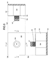
FIG. 6 shows a step in the example of the manufacturing process, wherein (a), (b) and (c) are a top plan view, a cross-sectional view taken along the line X-X' in (a), and a cross-sectional view taken along the line Y-Y' in (a), respectively. -
FIG. 7 shows a step in the example of the manufacturing process, wherein (a), (b) and (c) are a top plan view, a cross-sectional view taken along the line X-X' in (a), and a cross-sectional view taken along the line Y-Y' in (a), respectively. -
FIG. 8 shows a step in the example of the manufacturing process, wherein (a), (b) and (c) are a top plan view, a cross-sectional view taken along the line X-X' in (a), and a cross-sectional view taken along the line Y-Y' in (a), respectively. -
FIG. 9 shows a step in the example of the manufacturing process, wherein (a), (b) and (c) are a top plan view, a cross-sectional view taken along the line X-X' in (a), and a cross-sectional view taken along the line Y-Y' in (a), respectively. -
FIG. 10 shows a step in the example of the manufacturing process, wherein (a), (b) and (c) are a top plan view, a cross-sectional view taken along the line X-X' in (a), and a cross-sectional view taken along the line Y-Y' in (a), respectively. -
FIG. 11 shows a step in the example of the manufacturing process, wherein (a), (b) and (c) are a top plan view, a cross-sectional view taken along the line X-X' in (a), and a cross-sectional view taken along the line Y-Y' in (a), respectively. -
FIG. 12 shows a step in the example of the manufacturing process, wherein (a), (b) and (c) are a top plan view, a cross-sectional view taken along the line X-X' in (a), and a cross-sectional view taken along the line Y-Y' in (a), respectively. -
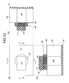
FIG. 13 shows a step in the example of the manufacturing process, wherein (a), (b) and (c) are a top plan view, a cross-sectional view taken along the line X-X' in (a), and a cross-sectional view taken along the line Y-Y' in (a), respectively. -
FIG. 14 shows a step in the example of the manufacturing process, wherein (a), (b) and (c) are a top plan view, a cross-sectional view taken along the line X-X' in (a), and a cross-sectional view taken along the line Y-Y' in (a), respectively. -
FIG. 15 shows a step in the example of the manufacturing process, wherein (a), (b) and (c) are a top plan view, a cross-sectional view taken along the line X-X' in (a), and a cross-sectional view taken along the line Y-Y' in (a), respectively. -
FIG. 16 shows a step in the example of the manufacturing process, wherein (a), (b) and (c) are a top plan view, a cross-sectional view taken along the line X-X' in (a), and a cross-sectional view taken along the line Y-Y' in (a), respectively. -
FIG. 17 shows a step in the example of the manufacturing process, wherein (a), (b) and (c) are a top plan view, a cross-sectional view taken along the line X-X' in (a), and a cross-sectional view taken along the line Y-Y' in (a), respectively. -
FIG. 18 shows a step in the example of the manufacturing process, wherein (a), (b) and (c) are a top plan view, a cross-sectional view taken along the line X-X' in (a), and a cross-sectional view taken along the line Y-Y' in (a), respectively. -
FIG. 19 shows a step in the example of the manufacturing process, wherein (a), (b) and (c) are a top plan view, a cross-sectional view taken along the line X-X' in (a), and a cross-sectional view taken along the line Y-Y' in (a), respectively. -
FIG. 20 shows a step in the example of the manufacturing process, wherein (a), (b) and (c) are a top plan view, a cross-sectional view taken along the line X-X' in (a), and a cross-sectional view taken along the line Y-Y' in (a), respectively. -
FIG. 21 shows a step in the example of the manufacturing process, wherein (a), (b) and (c) are a top plan view, a cross-sectional view taken along the line X-X' in (a), and a cross-sectional view taken along the line Y-Y' in (a), respectively. -
FIG. 22 shows a step in the example of the manufacturing process, wherein (a), (b) and (c) are a top plan view, a cross-sectional view taken along the line X-X' in (a), and a cross-sectional view taken along the line Y-Y' in (a), respectively. -
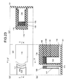
FIG. 23 shows a step in the example of the manufacturing process, wherein (a), (b) and (c) are a top plan view, a cross-sectional view taken along the line X-X' in (a), and a cross-sectional view taken along the line Y-Y' in (a), respectively. -
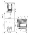
FIG. 24 shows a step in the example of the manufacturing process, wherein (a), (b) and (c) are a top plan view, a cross-sectional view taken along the line X-X' in (a), and a cross-sectional view taken along the line Y-Y' in (a), respectively. -
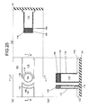
FIG. 25 shows a step in the example of the manufacturing process, wherein (a), (b) and (c) are a top plan view, a cross-sectional view taken along the line X-X' in (a), and a cross-sectional view taken along the line Y-Y' in (a), respectively. -
FIG. 26 shows a step in the example of the manufacturing process, wherein (a), (b) and (c) are a top plan view, a cross-sectional view taken along the line X-X' in (a), and a cross-sectional view taken along the line Y-Y' in (a), respectively. -
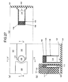
FIG. 27 shows a step in the example of the manufacturing process, wherein (a), (b) and (c) are a top plan view, a cross-sectional view taken along the line X-X' in (a), and a cross-sectional view taken along the line Y-Y' in (a), respectively. -
FIG. 28 shows a step in the example of the manufacturing process, wherein (a), (b) and (c) are a top plan view, a cross-sectional view taken along the line X-X' in (a), and a cross-sectional view taken along the line Y-Y' in (a), respectively. -
FIG. 29 shows a step in the example of the manufacturing process, wherein (a), (b) and (c) are a top plan view, a cross-sectional view taken along the line X-X' in (a), and a cross-sectional view taken along the line Y-Y' in (a), respectively. -
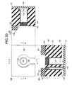
FIG. 30 shows a step in the example of the manufacturing process, wherein (a), (b) and (c) are a top plan view, a cross-sectional view taken along the line X-X' in (a), and a cross-sectional view taken along the line Y-Y' in (a), respectively. -
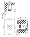
FIG. 31 shows a step in the example of the manufacturing process, wherein (a), (b) and (c) are a top plan view, a cross-sectional view taken along the line X-X' in (a), and a cross-sectional view taken along the line Y-Y' in (a), respectively. -
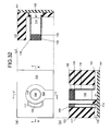
FIG. 32 shows a step in the example of the manufacturing process, wherein (a), (b) and (c) are a top plan view, a cross-sectional view taken along the line X-X' in (a), and a cross-sectional view taken along the line Y-Y' in (a), respectively. -
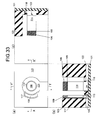
FIG. 33 shows a step in the example of the manufacturing process, wherein (a), (b) and (c) are a top plan view, a cross-sectional view taken along the line X-X' in (a), and a cross-sectional view taken along the line Y-Y' in (a), respectively. -
FIG. 34 shows a step in the example of the manufacturing process, wherein (a), (b) and (c) are a top plan view, a cross-sectional view taken along the line X-X' in (a), and a cross-sectional view taken along the line Y-Y' in (a), respectively. -
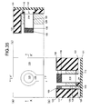
FIG. 35 shows a step in the example of the manufacturing process, wherein (a), (b) and (c) are a top plan view, a cross-sectional view taken along the line X-X' in (a), and a cross-sectional view taken along the line Y-Y' in (a), respectively. -
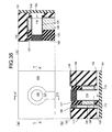
FIG. 36 shows a step in the example of the manufacturing process, wherein (a), (b) and (c) are a top plan view, a cross-sectional view taken along the line X-X' in (a), and a cross-sectional view taken along the line Y-Y' in (a), respectively. -
FIG. 37 shows a step in the example of the manufacturing process, wherein (a), (b) and (c) are a top plan view, a cross-sectional view taken along the line X-X' in (a), and a cross-sectional view taken along the line Y-Y' in (a), respectively. -
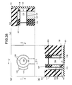
FIG. 38 shows a step in the example of the manufacturing process, wherein (a), (b) and (c) are a top plan view, a cross-sectional view taken along the line X-X' in (a), and a cross-sectional view taken along the line Y-Y' in (a), respectively. -
FIG. 39 shows a step in the example of the manufacturing process, wherein (a), (b) and (c) are a top plan view, a cross-sectional view taken along the line X-X' in (a), and a cross-sectional view taken along the line Y-Y' in (a), respectively. -
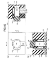
FIG. 40 shows a step in the example of the manufacturing process, wherein (a), (b) and (c) are a top plan view, a cross-sectional view taken along the line X-X' in (a), and a cross-sectional view taken along the line Y-Y' in (a), respectively. -
FIG. 41 shows a step in the example of the manufacturing process, wherein (a), (b) and (c) are a top plan view, a cross-sectional view taken along the line X-X' in (a), and a cross-sectional view taken along the line Y-Y' in (a), respectively. -
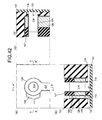
FIG. 42 shows a step in the example of the manufacturing process, wherein (a), (b) and (c) are a top plan view, a cross-sectional view taken along the line X-X' in (a), and a cross-sectional view taken along the line Y-Y' in (a), respectively.. -
FIG. 43 shows a step in the example of the manufacturing process, wherein (a), (b) and (c) are a top plan view, a cross-sectional view taken along the line X-X' in (a), and a cross-sectional view taken along the line Y-Y' in (a), respectively. -
FIG. 44 shows a step in the example of the manufacturing process, wherein (a), (b) and (c) are a top plan view, a cross-sectional view taken along the line X-X' in (a), and a cross-sectional view taken along the line Y-Y' in (a), respectively. -
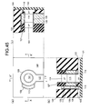
FIG. 45 shows a step in the example of the manufacturing process, wherein (a), (b) and (c) are a top plan view, a cross-sectional view taken along the line X-X' in (a), and a cross-sectional view taken along the line Y-Y' in (a), respectively. -
FIG. 46 shows a step in the example of the manufacturing process, wherein (a), (b) and (c) are a top plan view, a cross-sectional view taken along the line X-X' in (a), and a cross-sectional view taken along the line Y-Y' in (a), respectively. -
FIG. 47 shows a step in the example of the manufacturing process, wherein (a), (b) and (c) are a top plan view, a cross-sectional view taken along the line X-X' in (a), and a cross-sectional view taken along the line Y-Y' in (a), respectively. -
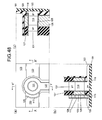
FIG. 48 shows a step in the example of the manufacturing process, wherein (a), (b) and (c) are a top plan view, a cross-sectional view taken along the line X-X' in (a), and a cross-sectional view taken along the line Y-Y' in (a), respectively. -
FIG. 49 shows a step in the example of the manufacturing process, wherein (a), (b) and (c) are a top plan view, a cross-sectional view taken along the line X-X' in (a), and a cross-sectional view taken along the line Y-Y' in (a), respectively. -
FIG. 50 shows a step in the example of the manufacturing process, wherein (a), (b) and (c) are a top plan view, a cross-sectional view taken along the line X-X' in (a), and a cross-sectional view taken along the line Y-Y' in (a), respectively. -
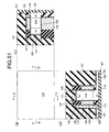
FIG. 51 shows a step in the example of the manufacturing process, wherein (a), (b) and (c) are a top plan view, a cross-sectional view taken along the line X-X' in (a), and a cross-sectional view taken along the line Y-Y' in (a), respectively. -
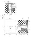
FIG. 52 shows a step in the example of the manufacturing process, wherein (a), (b) and (c) are a top plan view, a cross-sectional view taken along the line X-X' in (a), and a cross-sectional view taken along the line Y-Y' in (a), respectively. -
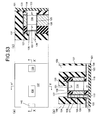
FIG. 53 shows a step in the example of the manufacturing process, wherein (a), (b) and (c) are a top plan view, a cross-sectional view taken along the line X-X' in (a), and a cross-sectional view taken along the line Y-Y' in (a), respectively. -
FIG. 54 shows a step in the example of the manufacturing process, wherein (a), (b) and (c) are a top plan view, a cross-sectional view taken along the line X-X' in (a), and a cross-sectional view taken along the line Y-Y' in (a), respectively. -
FIG. 55 shows a step in the example of the manufacturing process, wherein (a), (b) and (c) are a top plan view, a cross-sectional view taken along the line X-X' in (a), and a cross-sectional view taken along the line Y-Y' in (a), respectively. -
FIG. 56 shows a step in the example of the manufacturing process, wherein (a), (b) and (c) are a top plan view, a cross-sectional view taken along the line X-X' in (a), and a cross-sectional view taken along the line Y-Y' in (a), respectively. - An explanation will be given of a semiconductor device according to an embodiment of the present invention and a manufacturing method thereof with reference to the accompanying drawings.
-
FIG. 1 shows a semiconductor device according to one embodiment of the present invention, wherein (a), (b) and (c) are a schematic diagram of the semiconductor device in a plane view, taken along the line X-X' in (a) and a cross-sectional view taken along the line Y-Y' in (a), respectively. - As shown in
FIG. 1 , the semiconductor device of the present embodiment has a CMOS inverter circuit using an SGT, and comprises a first transistor which is an enhancement-type nMOS transistor that forms a channel between a source and a drain as a voltage is applied to a gate to prompt formation of an inversion layer, and a second transistor which is an enhancement-type pMOS transistor. - The first transistor includes an
island silicon layer 114 having the source, the gate, and the drain all arranged in the vertical direction relative to a substrate (not illustrated). - The first transistor further includes a first gate insulating film 125a surrounding the periphery of the
island silicon layer 114, agate electrode 126 surrounding the periphery of the first gate insulating film 125a, a first p+-type (first-conductivity-type)silicon layer 131 formed in an upper part of theisland silicon layer 114, and a second p+-type silicon layer 122 formed below theisland silicon layer 114. - The second transistor includes the
gate electrode 126, a second gate insulating film 125b surrounding a part of the periphery of thegate electrode 126, a secondarcuate silicon layer 113 contacting a part of the periphery of the second gate insulating film 125b, a first n+-type (second-conductivity-type)silicon layer 129 formed in an upper part of the secondarcuate silicon layer 113, and a second n+-type silicon layer 120 formed below the secondarcuate silicon layer 113. - The semiconductor device of the present embodiment further includes a first silicon/
metal compound layer 135 formed on the first p+-type silicon layer 131. - A second silicon/
metal compound layer 136 is formed on an extending part of the second p+-type silicon layer 122 running outwardly (in a direction apart from the island silicon layer 114) and in the horizontal direction. The semiconductor device of the present embodiment further includes thesecond compound layer 136. - The semiconductor device of the present embodiment further includes a third silicon/
metal compound layer 134 formed on the first n+-type silicon layer 129. - A fourth silicon/
metal compound layer 133 is formed on an extending part of the second n+-type silicon layer 120 running outwardly (in a direction apart from the island silicon layer 114) and in the horizontal direction. The semiconductor device of the present embodiment further includes thefourth compound layer 133. - The semiconductor device of the present embodiment further includes a
first contact 143 which is formed on the first silicon/metal compound layer 135 and on the third silicon/metal compound layer 134, and which electrically connects the p+-type silicon layer 131 in the first transistor and the n+-type silicon layer 129 in the second transistor. - The semiconductor device of the present embodiment further includes a
second contact 144 formed on the second silicon/metal compound layer 136 and electrically connected thereto, athird contact 142 formed on the fourth silicon/metal compound layer 133 and electrically connected to thereto, afourth contact 145 formed on thegate electrode 126, anoutput wiring 147 electrically connected to thefirst contact 143, aninput wiring 149 connected to thefourth contact 145, a first power-source wiring 148 connected to thesecond contact 144, and a second power-source wiring 146 connected to thethird contact 142. Theoutput wiring 147 is for outputting a signal to the exterior, and theinput wiring 149 is for inputting a signal from the exterior. The first power-source wiring 148 and the second power-source wiring 146 are used for electrically connecting an external DC power source or the like and the semiconductor device of the present embodiment together. - Note that the
first contact 143 may be formed as physically separated independent contacts which are connected to thefirst compound layer 135 and thethird compound layer 134, respectively. - According to the semiconductor device of the present invention, a pMOS SGT which is a pMOS transistor is configured by the first gate insulating film 125a surrounding the periphery of the
island silicon layer 114, thegate electrode 126 surrounding the periphery of the first gate insulating film 125a, the first p+-type silicon layer 131 formed in an upper part of theisland silicon layer 114, and the second p+-type silicon layer 122 formed below theisland silicon layer 114. - Moreover, according to the semiconductor device of the present embodiment, an nMOS SGT which is an nMOS transistor is configured by the
gate electrode 126, the second gate insulating film 125b surrounding a part of the periphery of thegate electrode 126, the secondarcuate silicon layer 113 contacting a part of the periphery of the secondgate insulating film 125, the first n+-type silicon layer 129 formed in an upper part of the secondarcuate silicon layer 113, and the second n+-type silicon layer 120 formed below the secondarcuate silicon layer 113. - With reference to
FIG. 1 , according to the semiconductor device of the present embodiment, Wp ≅ 2Wn is satisfied where Wn is the length of an arc formed at a boundary where the secondarcuate silicon layer 113 contacts a part of the periphery of the second gate insulating film 125b and Wp is the outer circumference length of theisland silicon layer 114. Moreover, according to the semiconductor device of the present embodiment, Ln ≅ Lp is satisfied where Ln is the channel length of the secondarcuate silicon layer 113 and Lp is the channel length of theisland silicon layer 114. By setting conditions which satisfy Wp ≅ 2Wn and Ln ≅ Lp as explained above, the gate width of the pMOS transistor becomes twice as much as that of the nMOS transistor, and because the mobility of a hole is half of that of an electron, the current drive force of the nMOS transistor can be made same as that of the pMOS transistor, so that the threshold voltage of an inverter can be set to be half of a supply voltage. - Note that according to the semiconductor device of the present embodiment, Wp > Wn and Ln ≅ Lp may be both satisfied where Wn is the length of the arc formed at the boundary where the second
arcuate semiconductor 113 contacts a part of the periphery of the second gate insulating film 125b and Wp is the outer circumference length of theisland silicon layer 114. Accordingly, it becomes also possible to accomplish high-integration of the semiconductor device comprising a CMOS inverter circuit using an SGT with the gate width of the pMOS transistor being wider than that of the nMOS transistor. - Moreover, according to the semiconductor device of the present embodiment, the first transistor is the enhancement-type nMOS transistor that includes the first gate insulating film 125a, the
gate electrode 126, theisland silicon layer 114, the first p+-type silicon layer 131, and the second p+-type silicon layer 122. Furthermore, the second transistor is the enhancement-type pMOS transistor that includes thegate electrode 126, the second gate insulating film 125b, the secondarcuate silicon layer 113, the first n+-type silicon layer 129, and the second n+-type silicon layer 120. - According to the semiconductor device of the present embodiment, as the
gate electrode 126 is formed of a material that causes the nMOS transistor and the pMOS transistor to be an enhancement type transistor, e.g., A1 (aluminum), and a cutoff state (non-conduction state) can be acquired between a source and a drain of the nMOS transistor and between those of the pMOS transistor by applying no voltage to thegate electrode 126. - An example of a manufacturing process of forming a structure of the semiconductor device of the present invention will be explained below with reference to
FIGS. 2 to 56 . Note that the same structural elements are denoted by the same reference numerals through these drawings.FIGS. 2 to 56 are diagrams for explaining the manufacturing process of the semiconductor device of the present invention. InFIGS. 2 to 56 , all A-figures are a plan view for explaining the manufacturing process of the semiconductor device according to the embodiment of the present invention, all B-figures are a cross-sectional view of corresponding A-figure along a line X-X', and all C-figures are a cross-sectional view of corresponding A-figure along a line Y-Y'. - With reference to
FIG. 2 , a resist 103 having a predetermined pattern for forming an n-type silicon layer is formed on a p-type ornon-doped silicon layer 102 formed on anoxide film 101. When thesilicon layer 102 is a non-doped silicon layer, this step is unnecessary. - Next, with reference to
FIG. 3 , phosphorus (P) is doped to form an n-type silicon layer 104 at a predetermined site of thesilicon layer 102 using the resist 103 as a mask. Thereafter, the resist 103 is peeled. When thesilicon layer 102 is a non-doped silicon layer, this step is unnecessary. - Next, with reference to
FIG. 4 , anoxide film 105 and anitride film 106 are formed on thesilicon layer 102 in this order. - Next, with reference to
FIG. 5 , a resist 107 having a predetermined pattern for forming a silicon column which will be theisland silicon layer 114 is formed at a predetermined position on thesilicon layer 102. - Next, with reference to
FIG. 6 , theoxide film 105 and thenitride film 106 are etched to be reshaped using the resist 107 as a mask. - Next, with reference to
FIG. 7 , the resist 107 is peeled. - Next, with reference to
FIG. 8 , anoxide film 108 is deposited on thesilicon layer 102 so as to cover theoxide film 105 and thenitride film 106. - Next, with reference to
FIG. 9 , theoxide film 108 is subjected to etch-back through reactive ion etching so as to be left around theoxide film 105 and thenitride film 106. - Next, with reference to
FIG. 10 , anitride film 109 is deposited so as to cover theoxide film 105, thenitride film 106, and theoxide film 108. - Next, with reference to
FIG. 11 , thenitride film 109 is subjected to etch-back through reactive ion etching so as to be left around theoxide film 108. - Next, with reference to
FIG. 12 , a resist 110 having a predetermined pattern for forming the secondarcuate silicon layer 113 is formed on theoxide film 105, thenitride film 106, theoxide film 108, and thenitride film 109. - Next, with reference to
FIG. 13 , thenitride film 109 is etched so as to be left at the sidewall of theoxide film 108 using the resist 110 as a mask. - Next, with reference to
FIG. 14 , the resist 110 is peeled. - Next, with reference to
FIG. 15 , resists 111 and 112 each having a predetermined pattern are formed on thesilicon layer 102 so as to cover a part of theoxide film 105, a part of thenitride film 106, a part of theoxide film 108, and a part of thenitride film 109. - Next, with reference to
FIG. 16 , only theoxide film 108 is selectively etched and eliminated using the resists 111 and 112 as masks. - Next, with reference to
FIG. 17 , the silicon at the surface layer of thesilicon layer 102 is etched and eliminated through a space where the eliminatedoxide film 108 was present. - Next, with reference to
FIG. 18 , the resists 111 and 112 are peeled. - Next, with reference to
FIG. 19 , theoxide film 108 is etched and eliminated. - Next, with reference to
FIG. 20 , the silicon of thesilicon layer 102 is etched to a predetermined depth by anisotropic etching using theoxide film 106 and thenitride film 109 as etching resists. Accordingly, theisland silicon layer 114, the secondarcuate silicon layer 113, and a p-type ornon-doped silicon layer 115 are formed. - Next, with reference to
FIG. 21 , anitride film 116 is deposited so as to thinly cover thenitride film 109, thenitride film 106, theisland silicon layer 114, the secondarcuate silicon layer 113, and the p-type ornon-doped silicon layer 115 with a uniform thickness. - Next, with reference to
FIG. 22 , thenitride film 116 is etched by anisotropic etching so as to be left as a sidewall spacer at respective sidewalls of theisland silicon layer 114 and the secondarcuate silicon layer 113, thereby forming nitride-film sidewalls - Next, with reference to
FIG. 23 , a resist 119 for impurity doping is formed so as to cover theisland silicon layer 114 over the nitride-film sidewall 118 and thenitride film 106. - Next, with reference to
FIG. 24 , arsenic (As) is doped to an extending part of the secondarcuate silicon layer 113 running outwardly (in a direction apart from the island silicon layer 114) and in the horizontal direction to form the n+-type silicon layer 120 using the resist 119 as a mask. - Next, with reference to
FIG. 25 , the resist 119 is peeled. - Next, with reference to
FIG. 26 , a resist 121 for impurity doping is formed so as to cover the secondarcuate silicon layer 113 over the nitride-film sidewall 117 and thenitride film 109. - Next, with reference to
FIG. 27 , boron (B) is doped to an extending part of theisland silicon layer 114 running outwardly of a columnar part thereof (in a direction apart from the columnar part of the island silicon layer 114) and in the horizontal direction to form the p+-type silicon layer 122 using the resist 121 as a mask. - Next, with reference to
FIG. 28 , the resist 121 is peeled. - Next, with reference to
FIG. 29 , anoxide film 123 is deposited until it exceeds a height of the columnar part of the secondarcuate silicon layer 113 and that of theisland silicon layer 114 so as to fill a space present around the sidewall of the columnar part of the secondarcuate silicon layer 113 and that of theisland silicon layer 114, and planarized by CMP (Chemical Mechanical Polishing) - Next, with reference to
FIG. 30 , a resist 124 having a predetermined pattern for etching a gate part is formed at predetermined positions on theoxide film 123 and on the secondarcuate silicon layer 113. - Next, with reference to
FIG. 31 , theoxide film 123 around theisland silicon layer 114 is etched to a predetermined depth and eliminated. - Next, with reference to
FIG. 32 , the resist 124 is peeled. - Next, with reference to
FIG. 33 , the nitride-film sidewall 118 at the sidewall of theisland silicon layer 114 and the nitride-film sidewall 117 at the sidewall of the secondarcuate silicon layer 113 are etched and eliminated. - Next, with reference to
FIG. 34 , ahigh dielectric film 125 which will be the first gate insulating film 125a and the second gate insulating film 125b, and, themetal 126 like aluminum for forming thegate electrode 126 are all deposited on theisland silicon layer 114, on the secondarcuate silicon layer 113, and on theoxide film 123, and planarized by CMP. - Next, with reference to
FIG. 35 , themetal 126 around theisland silicon layer 114 is subjected to etch-back to a predetermined depth (a center position of the height direction of the islands silicon layer 114). - Next, with reference to
FIG. 36 , anoxide film 127 is deposited in a space where themetal 126 subjected to etch-back was eliminated, and planarized by CMP. - Next, with reference to
FIG. 37 , thehigh dielectric film 125 exposed on a surface layer is etched and eliminated. - Next, with reference to
FIG. 38 , thenitride film 106 on theisland silicon layer 114, thenitride film 109 on the secondarcuate silicon layer 113, and the nitride-film sidewall 117 at the sidewall of the secondarcuate silicon layer 113 are etched and eliminated. - Next, with reference to
FIG. 39 , theoxide film 105 on theisland silicon layer 114 is etched and eliminated. - Next, with reference to
FIG. 40 , a resist 128 having a predetermined pattern for impurity doping is formed so as to fill a space above theisland silicon layer 114. - Next, with reference to
FIG. 41 , arsenic (As) is doped to the secondarcuate silicon layer 113 to form the n+-type silicon layer 129 using the resist 128 as a mask. - Next, with reference to
FIG. 42 , the resist 128 is peeled. - Next, with reference to
FIG. 43 , a resist 130 having a predetermined pattern for impurity doping is formed at a predetermined position except the space above theisland silicon layer 114. - Next, with reference to
FIG. 44 , boron (B) is doped to theisland silicon layer 114 to form the p+-type silicon layer 131. - Next, with reference to
FIG. 45 , the resist 130 is peeled. - Next, with reference to
FIG. 46 , a resist 132 for etching the oxide film is formed so as to fill the space above theisland silicon layer 114 and to partially fill a space above the secondarcuate silicon layer 113. - Next, with reference to
FIG. 47 , theoxide film 123 is etched and eliminated. - Next, with reference to
FIG. 48 , the resist 130 is peeled. - Next, with reference to
FIG. 49 , theoxide film 123 which remained in the etching step inFIG. 47 is etched to be removed. - Next, with reference to
FIG. 50 , the first silicon/metal compound layer 133, the second silicon/metal compound layer 134, the third silicon/metal compound layer 135, and the fourth silicon/metal compound layer 136 are formed on the n+-type silicon layer 120, on the n+-type silicon layer 129, on the p+-type silicon layer 131, and on the p+-type silicon layer 122, respectively. Ni (nickel) Co (cobalt) can be used as the metal, and the compound layer can be formed by, for example, depositing a nickel film on the silicon and applying a heat treatment to form an Ni silicide layer on the surface of the silicon. - Next, with reference to
FIG. 51 , aninterlayer film 137 is deposited over the first to fourth silicon/metal compound layers 133 to 136, theoxide film 127 and the like. - Next, with reference to
FIG. 52 , acontact hole 138 is formed so as to allow a space above the secondarcuate silicon layer 113 including the second silicon/metal compound layer 134 and the third silicon/metal compound layer 135 to be exposed. - Next, with reference to
FIG. 53 , contact holes 139 and 140 are formed so as to allow the first silicon/metal compound layer 133 and the fourth silicon/metal compound layer 136 to be exposed. - Next, with reference to
FIG. 54 , acontact hole 141 is formed so as to allow a part of themetal 126 around theisland silicon layer 114 to be exposed. - Next, with reference to
FIG. 55 ,contacts - Next, with reference to
FIG. 56 , the first power-source wiring 148 and the second power-source wiring 146 are formed so as to be electrically connected to thecontacts input wiring 149 and theoutput wiring 147 are formed so as to be electrically connected to thecontacts
Through the foregoing steps, the structure (see,FIG. 1 ) of the semiconductor device according to the embodiment of the present invention is thus formed. - The present invention is not limited to the foregoing embodiment, and can be changed and modified in various forms. The structure of the element is just an example, and can be changed as needed.
Having described and illustrated the principles of this application by reference to one preferred embodiment, it should be apparent that the preferred embodiment may be modified in arrangement and detail without departing from the principles disclosed herein and that it is intended that the application be construed as including all such modifications and variations insofar as they come within the spirit and scope of the subject matter disclosed herein.
Claims (14)
- A semiconductor device characterized by comprising a first transistor and a second transistor and being allowed by the first and second transistors to function as an inverter, wherein
the first transistor includes:an island semiconductor layer (114);a first gate insulating film (125) surrounding a periphery of the island semiconductor layer (114);a gate electrode (126) surrounding a periphery of the first gate insulating film (125);a first-conductivity-type upper high-concentration semiconductor layer (131) formed in an upper part of the island semiconductor layer (114); anda first-conductivity-type lower high-concentration semiconductor layer (122) formed in a lower part of the island semiconductor layer (114);the second transistor includes:the gate electrode (126);a second gate insulating film (125) surrounding at least a part of a periphery of the gate electrode (126);a semiconductor layer (113) contacting at least a part of a periphery of the second gate insulating film (125);a second-conductivity-type upper high-concentration semiconductor layer (129) which is formed in an upper part of the semiconductor layer (129) and which has an opposite conductivity to the first-conductivity-type upper high-concentration semiconductor layer (131); anda second-conductivity-type lower high-concentration semiconductor layer (120) which is formed in a lower part of the semiconductor layer (113) and which has an opposite conductivity to the first-conductivity-type lower high-concentration semiconductor layer (122), andthe semiconductor device further comprises a first contact (143) which electrically connects the first-conductivity-type upper high-concentration semiconductor layer (131) in the first transistor and the second-conductivity-type upper high-concentration semiconductor layer (129) in the second transistor together. - A semiconductor device characterized by comprising a first transistor and a second transistor and being allowed by the first second transistors to function as an inverter, wherein
the first transistor includes:an island semiconductor layer (114);a first gate insulating film (125) surrounding a periphery of the island semiconductor layer (114);a gate electrode (126) surrounding a periphery of the first gate insulating film (125);a first-conductivity-type upper high-concentration semiconductor layer (131) formed in an upper part of the island semiconductor layer (114); anda first-conductivity-type lower high-concentration semiconductor layer (122) formed in a lower part of the island semiconductor layer (114);the second transistor includes:the gate electrode (126);a gate insulating film (125) surrounding at least a part of a periphery of the gate electrode (126);an arcuate semiconductor layer (113) contacting a part of a periphery of the gate insulating film (125);a second-conductivity-type upper high-concentration semiconductor layer (129) which is formed in an upper part of the arcuate semiconductor layer (113) and which has an opposite conductivity to the first-conductivity-type upper high-concentration semiconductor layer (131); anda second-conductivity-type lower high-concentration semiconductor layer (120) which is formed in a lower part of the arcuate semiconductor layer (113) and which has an opposite conductivity to the first-conductivity-type lower high-concentration semiconductor layer (122),the semiconductor device further comprises a first contact (143) which electrically connects the first-conductivity-type upper high-concentration semiconductor layer (131) in the first transistor and the second-conductivity-type upper high-concentration semiconductor layer (129) in the second transistor together. - A semiconductor device characterized by comprising a first transistor and a second transistor and being allowed by the first second transistors to function as an inverter, wherein
the first transistor includes:an island semiconductor layer (114);a first gate insulating film (125) surrounding a periphery of the island semiconductor layer (114);a gate electrode (126) surrounding a periphery of the first gate insulating film (125);a first-conductivity-type upper high-concentration semiconductor layer (131) formed in an upper part of the island semiconductor layer (114); anda first-conductivity-type lower high-concentration semiconductor layer (122) formed in a lower part of the island semiconductor layer (114);the second transistor includes:the gate electrode (126);a second gate insulating film (125) surrounding at least a part of a periphery of the gate electrode (126);an arcuate semiconductor layer (113) contacting a part of a periphery of the second gate insulating film (125);a second-conductivity-type upper high-concentration semiconductor layer (129) which is formed in an upper part of the arcuate semiconductor layer (113) and which has an opposite conductivity to the first-conductivity-type upper high-concentration semiconductor layer (131); anda second-conductivity-type lower high-concentration semiconductor layer (120) which is formed in a lower part of the arcuate semiconductor layer (113) and which has an opposite conductivity to the first-conductivity-type lower high-concentration semiconductor layer (122),the semiconductor device further comprises:a first semiconductor/metal compound layer (135) formed on the first-conductivity-type upper high-concentration semiconductor layer (131) in the first transistor;a second semiconductor/metal compound layer (136) formed on an extending part of the first-conductivity-type lower high-concentration semiconductor layer (122) in the first transistor running outwardly of the first transistor and in a horizontal direction of the first transistor;a third semiconductor/metal compound layer (134) formed on the second-conductivity-type upper high-concentration semiconductor layer (129) in the second transistor;a fourth semiconductor/metal compound layer (133) formed on an extending part of the second-conductivity-type lower high-concentration semiconductor layer (120) in the second transistor running outwardly of the second transistor and in a horizontal direction of the second transistor;a first contact (143) which is formed on the first semiconductor/metal compound layer (135) and on the third semiconductor/metal compound layer (134) and which electrically connects the first-conductivity-type upper high-concentration semiconductor layer (131) in the first transistor and the second-conductivity-type upper high-concentration semiconductor layer (129) in the second transistor together; andan output wiring (147) electrically connected to the first contact (143). - The semiconductor device according to claim 3, characterized by further comprising:a second contact (144) formed on the second semiconductor/metal compound layer (136);a third contact (142) formed on the fourth semiconductor/metal compound layer (133);a fourth contact (145) formed on the gate electrode;the output wiring (147) which is connected to the first contact (143) and which is for outputting a signal;an input wiring (149) which is connected to the fourth contact (145) and which is for inputting a signal;a first power-source wiring (148) connected to the second contact (144) and to an external power source; anda second power-source wiring (146) connected to the third contact (142) and to an external power source.
- The semiconductor device according to claim 1, characterized in that
the first-conductivity-type upper high-concentration semiconductor layer (131) is a p+-type semiconductor layer,
the first-conductivity-type lower high-concentration semiconductor layer (122) is a p+-type semiconductor layer,
the second-conductivity-type upper high-concentration semiconductor layer (129) is an n+-type semiconductor layer, and
the second-conductivity-type lower high-concentration semiconductor layer (120) is an n+-type semiconductor layer. - The semiconductor device according to claim 3, characterized in that Wp ≅ 2 × Wn is satisfied where Wn is a length of an arc formed at a boundary where the arcuate semiconductor layer (113) contacts a part of the periphery of the second gate insulating film (125) and Wp is an outer circumference length of the island semiconductor layer.
- The semiconductor device according to claim 3, characterized in that when a length of an arc formed at a boundary where the arcuate semiconductor layer (113) contacts a part of the periphery of the second gate insulating film (125) is Wn and an outer circumference length of the island semiconductor layer is Wp, Wp is larger than Wn.
- The semiconductor device according to claim 3, characterized in that Ln ≅ Lp is satisfied where Ln is a channel length of the arcuate semiconductor layer (113) and Lp is a channel length of the island semiconductor layer (114).
- The semiconductor device according to claim 3, characterized in that Wp ≅ 2Wn and Ln ≅ Lp are both satisfied where Ln is a channel length of the arcuate semiconductor layer (113) and Lp is a channel length of the island semiconductor layer (114).
- The semiconductor device according to claim 3, characterized in that Wp > Wn and Ln ≅ Lp are both satisfied where Ln is a channel length of the arcuate semiconductor layer (113) and Lp is a channel length of the island semiconductor layer (114).
- The semiconductor device according to claim 1, characterized in that
the first transistor is an enhancement-type nMOS transistor,
the first-conductivity-type upper high-concentration semiconductor layer (131) is a p+-type semiconductor layer,
the first-conductivity-type lower high-concentration semiconductor layer (122) is a p+-type semiconductor layer,
the second transistor is an enhancement-type pMOS transistor,
the second-conductivity-type upper high-concentration semiconductor layer (129) is an n+-type semiconductor layer, and
the second-conductivity-type lower high-concentration semiconductor layer (120) is an n+-type semiconductor layer, and
the gate electrode (126) is formed of a material that causes the nMOS transistor and the pMOS transistor to be an enhancement-type transistor. - The semiconductor device according to claim 3, characterized in that all of the first to fourth semiconductor/metal compound layers (135,136,134,133) are a compound layer of silicon and metal.
- The semiconductor device according to claim 2, characterized in that
the first and second transistors are an enhancement-type nMOS transistor and an enhancement-type pMOS transistor, respectively,
the island semiconductor layer (114) is an island silicon layer,
the arcuate semiconductor layer (113) is an arcuate silicon layer,
both of the first-conductivity-type upper high-concentration semiconductor layer (131) and the first-conductivity-type lower high-concentration semiconductor layer (122) are a p+-type silicon layer, and
both of the second-conductivity-type upper high-concentration semiconductor layer (129) and the second-conductivity-type lower high-concentration semiconductor layer (120) are an n+-type silicon layer. - The semiconductor device according to claim 13, characterized in that
the island silicon layer (114) is an n-type or none-doped island silicon layer, and
the arcuate silicon layer (113) is a p-type or none-doped arcuate silicon layer.
Applications Claiming Priority (2)
| Application Number | Priority Date | Filing Date | Title |
|---|---|---|---|
| JP2009214166 | 2009-09-16 | ||
| JP2009297211A JP5006379B2 (en) | 2009-09-16 | 2009-12-28 | Semiconductor device |
Publications (2)
| Publication Number | Publication Date |
|---|---|
| EP2299494A2 true EP2299494A2 (en) | 2011-03-23 |
| EP2299494A3 EP2299494A3 (en) | 2012-03-28 |
Family
ID=43108259
Family Applications (1)
| Application Number | Title | Priority Date | Filing Date |
|---|---|---|---|
| EP10009573A Withdrawn EP2299494A3 (en) | 2009-09-16 | 2010-09-14 | Semiconductor device |
Country Status (6)
| Country | Link |
|---|---|
| US (1) | US8441066B2 (en) |
| EP (1) | EP2299494A3 (en) |
| JP (1) | JP5006379B2 (en) |
| KR (1) | KR101113904B1 (en) |
| CN (1) | CN102035533B (en) |
| TW (1) | TW201112397A (en) |
Families Citing this family (11)
| Publication number | Priority date | Publication date | Assignee | Title |
|---|---|---|---|---|
| SG165252A1 (en) | 2009-03-25 | 2010-10-28 | Unisantis Electronics Jp Ltd | Semiconductor device and production method therefor |
| JP5032532B2 (en) * | 2009-06-05 | 2012-09-26 | ユニサンティス エレクトロニクス シンガポール プライベート リミテッド | Semiconductor device and manufacturing method thereof |
| JP5006378B2 (en) * | 2009-08-11 | 2012-08-22 | ユニサンティス エレクトロニクス シンガポール プライベート リミテッド | Semiconductor device and manufacturing method thereof |
| US8759178B2 (en) | 2011-11-09 | 2014-06-24 | Unisantis Electronics Singapore Pte. Ltd. | Method for manufacturing semiconductor device and semiconductor device |
| US10438836B2 (en) | 2011-11-09 | 2019-10-08 | Unisantis Electronics Singapore Pte. Ltd. | Method for manufacturing a semiconductor device |
| JP5695745B2 (en) * | 2011-11-09 | 2015-04-08 | ユニサンティス エレクトロニクス シンガポール プライベート リミテッドUnisantis Electronics Singapore Pte Ltd. | Semiconductor device manufacturing method and semiconductor device |
| WO2013175557A1 (en) * | 2012-05-21 | 2013-11-28 | ユニサンティス エレクトロニクス シンガポール プライベート リミテッド | Semiconductor device |
| US8975705B2 (en) | 2012-05-21 | 2015-03-10 | Unisantis Electronics Singapore Pte. Ltd. | Semiconductor device |
| CN109768087B (en) * | 2018-12-20 | 2021-04-27 | 中国科学院微电子研究所 | Semiconductor device, method of manufacturing the same, integrated circuit, and electronic apparatus |
| CN112909020B (en) * | 2021-01-21 | 2023-04-07 | 武汉华星光电半导体显示技术有限公司 | Display panel and display device |
| US12439633B2 (en) * | 2022-08-31 | 2025-10-07 | International Business Machines Corporation | VTFET with controlled fin height |
Family Cites Families (45)
| Publication number | Priority date | Publication date | Assignee | Title |
|---|---|---|---|---|
| GB2052853A (en) * | 1979-06-29 | 1981-01-28 | Ibm | Vertical fet on an insulating substrate |
| JPS6070757A (en) * | 1983-09-28 | 1985-04-22 | Hitachi Ltd | Semiconductor integrated circuit |
| JPS60128654A (en) * | 1983-12-16 | 1985-07-09 | Hitachi Ltd | semiconductor integrated circuit |
| JPS6245058A (en) * | 1985-08-22 | 1987-02-27 | Nec Corp | Semiconductor device and its manufacture |
| US4890144A (en) * | 1987-09-14 | 1989-12-26 | Motorola, Inc. | Integrated circuit trench cell |
| JPH0266969A (en) * | 1988-08-31 | 1990-03-07 | Nec Corp | Semiconductor integrated circuit device |
| JP2703970B2 (en) * | 1989-01-17 | 1998-01-26 | 株式会社東芝 | MOS type semiconductor device |
| JPH03225873A (en) * | 1990-01-30 | 1991-10-04 | Mitsubishi Electric Corp | Semiconductor device |
| KR960001611B1 (en) * | 1991-03-06 | 1996-02-02 | 가부시끼가이샤 한도다이 에네르기 겐뀨쇼 | Insulated gate field effect semiconductor device and fabrication method thereof |
| US5466961A (en) * | 1991-04-23 | 1995-11-14 | Canon Kabushiki Kaisha | Semiconductor device and method of manufacturing the same |
| US5427962A (en) * | 1991-11-15 | 1995-06-27 | Casio Computer Co., Ltd. | Method of making a thin film transistor |
| EP0575280A3 (en) * | 1992-06-18 | 1995-10-04 | Ibm | Cmos transistor with two-layer inverse-t tungsten gate structure |
| JP2748072B2 (en) * | 1992-07-03 | 1998-05-06 | 三菱電機株式会社 | Semiconductor device and manufacturing method thereof |
| US5550084A (en) * | 1994-01-19 | 1996-08-27 | Advanced Micro Devices, Inc. | Integrated circuit fabrication using a metal silicide having a sputterdeposited metal nitride layer |
| JPH0851203A (en) | 1994-08-08 | 1996-02-20 | Mitsubishi Electric Corp | Semiconductor device and manufacturing method thereof |
| KR100193102B1 (en) * | 1994-08-25 | 1999-06-15 | 무명씨 | Semiconductor device and manufacturing method thereof |
| JPH098290A (en) * | 1995-06-20 | 1997-01-10 | Mitsubishi Electric Corp | Semiconductor device and manufacture thereof |
| US5773329A (en) * | 1996-07-24 | 1998-06-30 | International Business Machines Corporation | Polysilicon grown by pulsed rapid thermal annealing |
| US6235568B1 (en) * | 1999-01-22 | 2001-05-22 | Intel Corporation | Semiconductor device having deposited silicon regions and a method of fabrication |
| EP1063697B1 (en) * | 1999-06-18 | 2003-03-12 | Lucent Technologies Inc. | A process for fabricating a CMOS integrated circuit having vertical transistors |
| JP4811895B2 (en) * | 2001-05-02 | 2011-11-09 | ルネサスエレクトロニクス株式会社 | Semiconductor device and manufacturing method thereof |
| US6461900B1 (en) * | 2001-10-18 | 2002-10-08 | Chartered Semiconductor Manufacturing Ltd. | Method to form a self-aligned CMOS inverter using vertical device integration |
| EP1329946A3 (en) * | 2001-12-11 | 2005-04-06 | Sel Semiconductor Energy Laboratory Co., Ltd. | Manufacturing method of semiconductor device including a laser crystallization step |
| US6867084B1 (en) * | 2002-10-03 | 2005-03-15 | Taiwan Semiconductor Manufacturing Company, Ltd. | Gate structure and method of forming the gate dielectric with mini-spacer |
| JP2004319808A (en) * | 2003-04-17 | 2004-11-11 | Takehide Shirato | Mis field effect transistor and its manufacturing method |
| US6943407B2 (en) | 2003-06-17 | 2005-09-13 | International Business Machines Corporation | Low leakage heterojunction vertical transistors and high performance devices thereof |
| JP2005064031A (en) | 2003-08-12 | 2005-03-10 | Fujio Masuoka | Semiconductor device |
| US7309900B2 (en) * | 2004-03-23 | 2007-12-18 | Advanced Lcd Technologies Development Center Co., Ltd. | Thin-film transistor formed on insulating substrate |
| WO2005096381A1 (en) * | 2004-04-01 | 2005-10-13 | Soisic | Improved layout of a sram memory cell |
| JP2005310921A (en) | 2004-04-19 | 2005-11-04 | Okayama Prefecture | MOS type semiconductor device and manufacturing method thereof |
| US20060261406A1 (en) * | 2005-05-18 | 2006-11-23 | Yijian Chen | Vertical integrated-gate CMOS device and its fabrication process |
| JP2007250652A (en) * | 2006-03-14 | 2007-09-27 | Sharp Corp | Semiconductor device |
| JP2008066562A (en) | 2006-09-08 | 2008-03-21 | Toshiba Corp | Semiconductor device and manufacturing method thereof |
| JP5094099B2 (en) * | 2006-12-04 | 2012-12-12 | 株式会社半導体エネルギー研究所 | Method for manufacturing semiconductor device |
| JP5114968B2 (en) | 2007-02-20 | 2013-01-09 | 富士通セミコンダクター株式会社 | Semiconductor device and manufacturing method thereof |
| JP5130596B2 (en) * | 2007-05-30 | 2013-01-30 | 国立大学法人東北大学 | Semiconductor device |
| JP5122212B2 (en) | 2007-08-02 | 2013-01-16 | ユニサンティス エレクトロニクス シンガポール プライベート リミテッド | Semiconductor device |
| JP5204121B2 (en) * | 2007-10-29 | 2013-06-05 | ユニサンティス エレクトロニクス シンガポール プライベート リミテッド | Semiconductor structure and method of manufacturing the semiconductor structure |
| US20090146194A1 (en) * | 2007-12-05 | 2009-06-11 | Ecole Polytechnique Federale De Lausanne (Epfl) | Semiconductor device and method of manufacturing a semiconductor device |
| US8212298B2 (en) * | 2008-01-29 | 2012-07-03 | Unisantis Electronics Singapore Pte Ltd. | Semiconductor storage device and methods of producing it |
| US8053842B2 (en) * | 2008-01-29 | 2011-11-08 | Unisantis Electronics (Japan) Ltd. | Semiconductor storage device |
| WO2009096002A1 (en) * | 2008-01-29 | 2009-08-06 | Unisantis Electronics (Japan) Ltd. | Manufacturing method of semiconductor storage device |
| WO2009095997A1 (en) * | 2008-01-29 | 2009-08-06 | Unisantis Electronics (Japan) Ltd. | Semiconductor device and its manufacturing method |
| SG165252A1 (en) * | 2009-03-25 | 2010-10-28 | Unisantis Electronics Jp Ltd | Semiconductor device and production method therefor |
| JP5032532B2 (en) * | 2009-06-05 | 2012-09-26 | ユニサンティス エレクトロニクス シンガポール プライベート リミテッド | Semiconductor device and manufacturing method thereof |
-
2009
- 2009-12-28 JP JP2009297211A patent/JP5006379B2/en not_active Expired - Fee Related
-
2010
- 2010-09-14 TW TW099131001A patent/TW201112397A/en unknown
- 2010-09-14 EP EP10009573A patent/EP2299494A3/en not_active Withdrawn
- 2010-09-14 KR KR1020100089913A patent/KR101113904B1/en not_active Expired - Fee Related
- 2010-09-15 US US12/882,698 patent/US8441066B2/en active Active
- 2010-09-16 CN CN201010288977XA patent/CN102035533B/en active Active
Non-Patent Citations (1)
| Title |
|---|
| S. WATANABE; K. TSUCHIDA; D. TAKASHIMA; Y. OOWAKI; A. NITAYAMA; K. HIEDA; H. TAKATO; K. SUNOUCHI; F. HORIGUCHI; K. OHUCHI: "A Nobel Circuit Technology with Surrounding Gate Transistors (SGT's) for Ultra High Density DRAM's", IEEE JSSC, vol. 30, no. 9, 1995, XP000526202, DOI: doi:10.1109/4.406391 |
Also Published As
| Publication number | Publication date |
|---|---|
| JP5006379B2 (en) | 2012-08-22 |
| CN102035533B (en) | 2012-12-26 |
| KR20110030353A (en) | 2011-03-23 |
| US8441066B2 (en) | 2013-05-14 |
| CN102035533A (en) | 2011-04-27 |
| EP2299494A3 (en) | 2012-03-28 |
| TW201112397A (en) | 2011-04-01 |
| US20110062521A1 (en) | 2011-03-17 |
| JP2011086900A (en) | 2011-04-28 |
| KR101113904B1 (en) | 2012-02-29 |
Similar Documents
| Publication | Publication Date | Title |
|---|---|---|
| US8441066B2 (en) | Semiconductor device | |
| CN102034872B (en) | Semiconductor device | |
| EP2299484B1 (en) | Semiconductor device comprising surrounding gate transistors. | |
| TWI429060B (en) | Semiconductor device and method of manufacturing same | |
| KR101124060B1 (en) | Semiconductor device and production method therefor | |
| TWI394267B (en) | Semiconductor device | |
| WO2016031014A1 (en) | Semiconductor device, and method for manufacturing semiconductor device | |
| JP5006375B2 (en) | Semiconductor device and manufacturing method thereof | |
| JP5395748B2 (en) | Semiconductor device and manufacturing method thereof | |
| US8664063B2 (en) | Method of producing a semiconductor device and semiconductor device | |
| JP2007019200A (en) | Semiconductor device and its manufacturing method | |
| JP5926354B2 (en) | Semiconductor device | |
| JP5643900B2 (en) | Semiconductor device manufacturing method and semiconductor device | |
| JP6230648B2 (en) | Semiconductor device |
Legal Events
| Date | Code | Title | Description |
|---|---|---|---|
| PUAI | Public reference made under article 153(3) epc to a published international application that has entered the european phase |
Free format text: ORIGINAL CODE: 0009012 |
|
| AK | Designated contracting states |
Kind code of ref document: A2 Designated state(s): AL AT BE BG CH CY CZ DE DK EE ES FI FR GB GR HR HU IE IS IT LI LT LU LV MC MK MT NL NO PL PT RO SE SI SK SM TR |
|
| AX | Request for extension of the european patent |
Extension state: BA ME RS |
|
| RAP1 | Party data changed (applicant data changed or rights of an application transferred) |
Owner name: UNISANTIS ELECTRONICS SINGAPORE PTE. LTD. |
|
| PUAL | Search report despatched |
Free format text: ORIGINAL CODE: 0009013 |
|
| AK | Designated contracting states |
Kind code of ref document: A3 Designated state(s): AL AT BE BG CH CY CZ DE DK EE ES FI FR GB GR HR HU IE IS IT LI LT LU LV MC MK MT NL NO PL PT RO SE SI SK SM TR |
|
| AX | Request for extension of the european patent |
Extension state: BA ME RS |
|
| RIC1 | Information provided on ipc code assigned before grant |
Ipc: H01L 29/786 20060101ALI20120220BHEP Ipc: H01L 27/12 20060101ALI20120220BHEP Ipc: H01L 21/84 20060101ALI20120220BHEP Ipc: H01L 21/8238 20060101ALI20120220BHEP Ipc: H01L 29/78 20060101AFI20120220BHEP |
|
| 17P | Request for examination filed |
Effective date: 20120330 |
|
| RAP1 | Party data changed (applicant data changed or rights of an application transferred) |
Owner name: UNISANTIS ELECTRONICS SINGAPORE PTE. LTD. |
|
| STAA | Information on the status of an ep patent application or granted ep patent |
Free format text: STATUS: THE APPLICATION HAS BEEN WITHDRAWN |
|
| 18W | Application withdrawn |
Effective date: 20140205 |