EP2299478A1 - Laser annealing device - Google Patents
Laser annealing device Download PDFInfo
- Publication number
- EP2299478A1 EP2299478A1 EP09773305A EP09773305A EP2299478A1 EP 2299478 A1 EP2299478 A1 EP 2299478A1 EP 09773305 A EP09773305 A EP 09773305A EP 09773305 A EP09773305 A EP 09773305A EP 2299478 A1 EP2299478 A1 EP 2299478A1
- Authority
- EP
- European Patent Office
- Prior art keywords
- inert gas
- temperature
- gas
- workpiece
- laser light
- Prior art date
- Legal status (The legal status is an assumption and is not a legal conclusion. Google has not performed a legal analysis and makes no representation as to the accuracy of the status listed.)
- Withdrawn
Links
Images

Classifications
-
- H—ELECTRICITY
- H10—SEMICONDUCTOR DEVICES; ELECTRIC SOLID-STATE DEVICES NOT OTHERWISE PROVIDED FOR
- H10P—GENERIC PROCESSES OR APPARATUS FOR THE MANUFACTURE OR TREATMENT OF DEVICES COVERED BY CLASS H10
- H10P34/00—Irradiation with electromagnetic or particle radiation of wafers, substrates or parts of devices
- H10P34/40—Irradiation with electromagnetic or particle radiation of wafers, substrates or parts of devices with high-energy radiation
- H10P34/42—Irradiation with electromagnetic or particle radiation of wafers, substrates or parts of devices with high-energy radiation with electromagnetic radiation, e.g. laser annealing
-
- B—PERFORMING OPERATIONS; TRANSPORTING
- B23—MACHINE TOOLS; METAL-WORKING NOT OTHERWISE PROVIDED FOR
- B23K—SOLDERING OR UNSOLDERING; WELDING; CLADDING OR PLATING BY SOLDERING OR WELDING; CUTTING BY APPLYING HEAT LOCALLY, e.g. FLAME CUTTING; WORKING BY LASER BEAM
- B23K26/00—Working by laser beam, e.g. welding, cutting or boring
- B23K26/08—Devices involving relative movement between laser beam and workpiece
- B23K26/083—Devices involving movement of the workpiece in at least one axial direction
- B23K26/0853—Devices involving movement of the workpiece in at least two axial directions, e.g. in a plane
-
- B—PERFORMING OPERATIONS; TRANSPORTING
- B23—MACHINE TOOLS; METAL-WORKING NOT OTHERWISE PROVIDED FOR
- B23K—SOLDERING OR UNSOLDERING; WELDING; CLADDING OR PLATING BY SOLDERING OR WELDING; CUTTING BY APPLYING HEAT LOCALLY, e.g. FLAME CUTTING; WORKING BY LASER BEAM
- B23K26/00—Working by laser beam, e.g. welding, cutting or boring
- B23K26/12—Working by laser beam, e.g. welding, cutting or boring in a special environment or atmosphere, e.g. in an enclosure
- B23K26/127—Working by laser beam, e.g. welding, cutting or boring in a special environment or atmosphere, e.g. in an enclosure in an enclosure
-
- B—PERFORMING OPERATIONS; TRANSPORTING
- B23—MACHINE TOOLS; METAL-WORKING NOT OTHERWISE PROVIDED FOR
- B23K—SOLDERING OR UNSOLDERING; WELDING; CLADDING OR PLATING BY SOLDERING OR WELDING; CUTTING BY APPLYING HEAT LOCALLY, e.g. FLAME CUTTING; WORKING BY LASER BEAM
- B23K26/00—Working by laser beam, e.g. welding, cutting or boring
- B23K26/12—Working by laser beam, e.g. welding, cutting or boring in a special environment or atmosphere, e.g. in an enclosure
- B23K26/127—Working by laser beam, e.g. welding, cutting or boring in a special environment or atmosphere, e.g. in an enclosure in an enclosure
- B23K26/128—Laser beam path enclosures
-
- B—PERFORMING OPERATIONS; TRANSPORTING
- B23—MACHINE TOOLS; METAL-WORKING NOT OTHERWISE PROVIDED FOR
- B23K—SOLDERING OR UNSOLDERING; WELDING; CLADDING OR PLATING BY SOLDERING OR WELDING; CUTTING BY APPLYING HEAT LOCALLY, e.g. FLAME CUTTING; WORKING BY LASER BEAM
- B23K26/00—Working by laser beam, e.g. welding, cutting or boring
- B23K26/14—Working by laser beam, e.g. welding, cutting or boring using a fluid stream, e.g. a jet of gas, in conjunction with the laser beam; Nozzles therefor
- B23K26/1462—Nozzles; Features related to nozzles
- B23K26/1464—Supply to, or discharge from, nozzles of media, e.g. gas, powder, wire
- B23K26/147—Features outside the nozzle for feeding the fluid stream towards the workpiece
-
- B—PERFORMING OPERATIONS; TRANSPORTING
- B23—MACHINE TOOLS; METAL-WORKING NOT OTHERWISE PROVIDED FOR
- B23K—SOLDERING OR UNSOLDERING; WELDING; CLADDING OR PLATING BY SOLDERING OR WELDING; CUTTING BY APPLYING HEAT LOCALLY, e.g. FLAME CUTTING; WORKING BY LASER BEAM
- B23K26/00—Working by laser beam, e.g. welding, cutting or boring
- B23K26/70—Auxiliary operations or equipment
- B23K26/702—Auxiliary equipment
-
- B—PERFORMING OPERATIONS; TRANSPORTING
- B23—MACHINE TOOLS; METAL-WORKING NOT OTHERWISE PROVIDED FOR
- B23K—SOLDERING OR UNSOLDERING; WELDING; CLADDING OR PLATING BY SOLDERING OR WELDING; CUTTING BY APPLYING HEAT LOCALLY, e.g. FLAME CUTTING; WORKING BY LASER BEAM
- B23K2103/00—Materials to be soldered, welded or cut
- B23K2103/50—Inorganic materials other than metals or composite materials
- B23K2103/56—Inorganic materials other than metals or composite materials being semiconducting
-
- H—ELECTRICITY
- H10—SEMICONDUCTOR DEVICES; ELECTRIC SOLID-STATE DEVICES NOT OTHERWISE PROVIDED FOR
- H10P—GENERIC PROCESSES OR APPARATUS FOR THE MANUFACTURE OR TREATMENT OF DEVICES COVERED BY CLASS H10
- H10P14/00—Formation of materials, e.g. in the shape of layers or pillars
- H10P14/20—Formation of materials, e.g. in the shape of layers or pillars of semiconductor materials
- H10P14/34—Deposited materials, e.g. layers
- H10P14/3402—Deposited materials, e.g. layers characterised by the chemical composition
- H10P14/3404—Deposited materials, e.g. layers characterised by the chemical composition being Group IVA materials
- H10P14/3411—Silicon, silicon germanium or germanium
-
- H—ELECTRICITY
- H10—SEMICONDUCTOR DEVICES; ELECTRIC SOLID-STATE DEVICES NOT OTHERWISE PROVIDED FOR
- H10P—GENERIC PROCESSES OR APPARATUS FOR THE MANUFACTURE OR TREATMENT OF DEVICES COVERED BY CLASS H10
- H10P14/00—Formation of materials, e.g. in the shape of layers or pillars
- H10P14/20—Formation of materials, e.g. in the shape of layers or pillars of semiconductor materials
- H10P14/38—Formation of materials, e.g. in the shape of layers or pillars of semiconductor materials characterised by treatments done after the formation of the materials
- H10P14/3802—Crystallisation or recrystallisation of non-monocrystalline semiconductor materials, e.g. regrowth
- H10P14/3808—Crystallisation or recrystallisation of non-monocrystalline semiconductor materials, e.g. regrowth using laser beams
-
- H—ELECTRICITY
- H10—SEMICONDUCTOR DEVICES; ELECTRIC SOLID-STATE DEVICES NOT OTHERWISE PROVIDED FOR
- H10P—GENERIC PROCESSES OR APPARATUS FOR THE MANUFACTURE OR TREATMENT OF DEVICES COVERED BY CLASS H10
- H10P72/00—Handling or holding of wafers, substrates or devices during manufacture or treatment thereof
- H10P72/04—Apparatus for manufacture or treatment
- H10P72/0431—Apparatus for thermal treatment
- H10P72/0436—Apparatus for thermal treatment mainly by radiation
Definitions
- the present invention relates to a laser annealing apparatus for performing an annealing treatment on a workpiece to be processed by irradiating the workpiece with laser light.
- a thin film transistor in which a polysilicon film is used for a channel layer has been widely used as a switching element of a semiconductor device and a liquid crystal display.
- the polysilicon film used for the channel layer of the thin film transistor is generally manufactured using a process called a low-temperature polysilicon.
- the low-temperature polysilicon is a process of forming an amorphous silicon film on a glass substrate and irradiating the amorphous silicon film with a laser light to produce a polysilicon film.
- the amorphous silicon film is heated, melted, and recrystallized to produce a polysilicon film using a laser annealing apparatus.
- the low-temperature polysilicon has a problem in that if oxygen is included in the annealing atmosphere, the silicon is oxidized during heating to have an adverse effect on the device characteristics. For this reason, an operation of preventing oxidation of silicon using an inert gas such as nitrogen is performed.
- Patent Document 1 a stage on which a glass substrate is placed is provided in a processing chamber so as to supply nitrogen gas into the processing chamber, thus preventing oxidation of silicon during an annealing treatment.
- nitrogen is discharged from a tip end of a swing nozzle that swings up and down so as to create a nitrogen atmosphere only in the vicinity of a laser irradiation portion, thus preventing oxidation of silicon during an annealing treatment.
- Patent Document 3 in a state in which a cylindrical cell of which the top portion is sealed by glass and the bottom portion is open is disposed at a position sufficiently close to a substrate, nitrogen gas is filled into the cell, thus preventing oxidation of silicon during annealing.
- the present invention has been made in consideration of the above-mentioned problems, and an object of the present invention is to provide a laser annealing apparatus capable of reducing irradiation unevenness of laser light caused by a refraction phenomenon of laser light due to fluctuation (variation) in the temperature of inert gas.
- the laser annealing apparatus of the present invention apply the following means.
- the temperature of the inert gas supplied to the laser irradiation area is controlled by the gas temperature controller so as to approach the atmospheric temperature of a space (room) that is disposed outside the supply area of the inert gas so as to surround the optical path of the laser light.
- a space room
- the temperature difference between the room and the inert gas is preferably as low as possible and is most preferably zero.
- the purge box is disposed on the optical path of the laser light, although the laser light passes through the inert gas in the purge box during the annealing treatment, the temperature of the inert gas is controlled so as to approach the atmospheric temperature (temperature of the room) outside the purge box before the inert gas is introduced into the purge box. Therefore, a refraction phenomenon of the laser light in the purge box is decreased, whereby irradiation unevenness is reduced.
- the inert gas is sprayed from the purge unit towards the workpiece during the annealing treatment, and the laser light passes through the inert gas, the temperature of the inert gas is controlled so as to approach the atmospheric temperature of the space outside the purge unit before the inert gas is sprayed towards the workpiece. Therefore, a refraction phenomenon of the laser light in the supply area of the inert gas is decreased, whereby irradiation unevenness is reduced.
- the temperature of the inert gas is controlled so as to approach the atmospheric temperature outside the processing chamber before the inert gas is introduced into the processing chamber. Therefore, a refraction phenomenon of the laser light in the processing chamber is decreased, whereby irradiation unevenness is reduced.
- the present invention it is possible to reduce irradiation unevenness of laser light caused by a refraction phenomenon of laser light due to fluctuation (variation) in the temperature of inert gas.
- Fig. 1 is a diagram illustrating an entire configuration of a laser annealing apparatus 1 according to an embodiment of the present invention.
- the laser annealing apparatus 1 includes, as its basic constituent elements, a laser light source 3 that emits laser light 2, a beam shaping optical system 4 that shapes the laser light 2 from the laser light source 3 into a desired beam shape, a reflecting mirror 5 that reflects the laser light 2 towards a workpiece to be processed 7, a condensing lens 6 that condenses the laser light 2 from the reflecting mirror 5 onto the surface of the workpiece 7, and a movable stage 9 that moves in a direction (direction indicated by arrow A in the figure) crossing the laser light 2 while carrying the workpiece 7.
- an excimer laser, a solid-state laser, or a semiconductor laser can be used, for example.
- the solid-state laser YAG, YLF, YVO 4 , and the like can be used.
- the laser light 2 may be either pulse oscillated or continuously oscillated.
- the beam shaping optical system 4 can be configured to shape the laser light 2 so as to have a linear or rectangular beam in sectional view on the surface of the workpiece 7, and in this case, can include a beam expander, a homogenizer, and the like as its constituent elements.
- the workpiece 7 includes a substrate 7a and an amorphous semiconductor film 7b formed thereon.
- the substrate 7a is a glass substrate or a semiconductor substrate.
- the amorphous semiconductor film 7b is an amorphous silicon film, for example.
- the laser light 2 is emitted from the laser light source 3, and the laser light 2 is condensed into a linear or rectangular beam by the beam shaping by the beam shaping optical system 4 and the condensing by the condensing lens 6 and irradiated onto the workpiece 7.
- the workpiece 7 is moved in the short-axis direction of the beam by the movable stage 9 so as to scan over the entire surface of the amorphous semiconductor film of the workpiece 7 at the laser irradiation portion.
- the amorphous semiconductor film 7b is crystallized.
- the amorphous silicon film is changed to a polysilicon film.
- the beam shape of the laser light 2 irradiated onto the workpiece 7 is not limited to the linear or rectangular beam, and it is possible to effectively perform an annealing treatment on the workpiece 7 having a large area by scanning the laser light 2 condensed into a linear or rectangular beam in the short-axis direction thereof.
- the laser annealing apparatus 1 of the present invention further includes a gas supply unit 10 that supplies an inert gas G to at least a laser irradiation area of the workpiece 7 and a gas temperature controller 15 that controls the temperature of the inert gas G.
- the inert gas G supplied from the gas supply unit 10 nitrogen, helium, neon, argon, krypton, xenon, radon, ununoctium, and the like can be used.
- the inert gas G is introduced to the gas supply unit 10 through a gas pipe 14 from a gas tank or a gas cylinder which is provided outside a room R in which the laser annealing apparatus 1 is provided. For this reason, the temperature of the inert gas G is generally different from the temperature of the room R.
- the gas temperature controller 15 controls the temperature of the inert gas G supplied to the laser irradiation area so as to decrease the temperature difference between the temperature of the inert gas G and the atmospheric temperature of a space that is disposed outside the supply area of the inert gas G so as to surround the optical path of the laser light 2.
- the gas temperature controller 15 preferably has a function of both heating and cooling the inert gas G.
- the space that is disposed outside the inert gas G so as to surround the optical path of the laser light 2 is generally the room R (for example, a cleanroom) in which the laser annealing apparatus 1 is provided, and the temperature thereof is the inside temperature of the room R.
- the temperature of the room R is detected by a temperature sensor 17 provided in the room R.
- the temperature detected by the temperature sensor 17 is converted into a temperature signal and transmitted to a control unit 16.
- the control unit 16 controls the gas temperature controller 15 so that the temperature of the inert gas G approaches the temperature of the room R.
- the temperature of the inert gas G supplied to the laser irradiation area is controlled by the gas temperature controller 15 so as to approach the atmospheric temperature of the space (room R) that is disposed outside the supply area of the inert gas G so as to surround the optical path of the laser light 2.
- the inert gas G when the temperature of the room R is relatively low by an air conditioner, and the temperature of the inert gas G supplied from a gas tank provided at a different place is relatively high, the inert gas G is cooled by the gas temperature controller. Moreover, for example, when the temperature of the room R is relatively high by an air conditioner, and the temperature of the inert gas G supplied from a gas tank provided at a different place is relatively low, the inert gas G is heated by the gas temperature controller.
- the temperature difference between the room R and the inert gas G is preferably as low as possible and is most preferably zero. Therefore, it is preferable to control the temperature of the inert gas G so as to be the same as the temperature of the room R with the gas temperature controller 15.
- the gas supply unit 10 may employ various forms as long as it has a function of supplying the inert gas G to at least the laser irradiation area of the workpiece 7.
- the gas supply unit 10 may employ various forms as long as it has a function of supplying the inert gas G to at least the laser irradiation area of the workpiece 7.
- several configuration examples of the gas supply unit 10 will be described, and the present invention is not limited to these configuration examples.
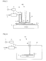
- Fig. 2 is a diagram illustrating a gas supply unit 10A according to a first configuration example.
- the gas supply unit 10A includes a purge box 11 of which the lower surface in the figure is disposed so as to face the surface of the workpiece 7 and in which the inert gas G is introduced.
- the purge box 11 includes a transmission window 12 (for example, a glass window) that transmits the laser light 2 so as to be introduced therein and an opening 13 that passes the introduced laser light 2 therethrough and blows the inside inert gas G towards the workpiece 7.
- a transmission window 12 for example, a glass window
- the lower surface of the purge box 11 is preferably a flat surface that is parallel to the surface of the workpiece 7, and the distance between the lower surface of the purge box 11 and the workpiece 7 is preferably sufficiently small (for example, within 5 mm) within a range where they do not come into contact.
- the gas temperature controller 15 controls the temperature of the inert gas G at a position located further upstream than the purge box 11.
- the purge box 11 is connected to a gas pipe 14 for introducing the inert gas G into the purge box 11, and the gas temperature controller 15 is provided in the way of the gas pipe 14.
- gas temperature controller 15 for example, heat pumping heating-cooling equipment and electronic heating-cooling equipment using a Peltier device can be used.
- the gas temperature controller 15 may be configured by a ribbon heater and a heating furnace. In this regard, the same statements can be applied to the second and third configuration examples.
- the purge box 11 is disposed on the optical path of the laser light 2, although the laser light 2 passes through the inert gas G in the purge box 11 during the annealing treatment, the temperature of the inert gas G is controlled so as to approach the atmospheric temperature (temperature of the room R) outside the purge box 11 before the inert gas G is introduced into the purge box 11. Therefore, the difference between the atmospheric temperature of the space surrounding the optical path of the laser light 2 and the temperature of the inert gas G inside the purge box 11 and in the purge area decreases, and a refraction phenomenon of the laser light 2 in the purge box 11 is decreased, whereby irradiation unevenness is reduced.
- Fig. 3 shows a gas supply unit 10B according to a second configuration example.
- the gas supply unit 10B includes a parallel facing body 18 of which the lower surface in the figure is disposed so as to face the surface of the workpiece 7 in parallel and a purge unit 22 that sprays the inert gas G towards the workpiece 7 so that the inert gas G is supplied between the parallel facing body 18 and the surface of the workpiece 7.
- the parallel facing body 18 includes a transmission window 20 (for example, a glass window) which is formed on a bottom portion 19 that forms the lower surface facing the workpiece 7 so as to transmit the laser light 2.
- the purge unit 22 has a void structure in which the inert gas G is introduced and has a discharge opening 23 which is formed on the bottom portion thereof so as to blow the inert gas G towards the workpiece 7.
- the purge unit 22 is mounted on the side portion of the parallel facing body 18.
- the gas temperature controller 15 controls the temperature of the inert gas G at a position located further upstream than the purge unit 22.
- the purge unit 22 is connected to a gas pipe 14 for introducing the inert gas G into the purge unit 22, and the gas temperature controller 15 is provided in the way of the gas pipe 14.
- the gas temperature controller may be provided inside the purge unit 22 so as to heat or cool the inert gas G inside the purge unit 22.
- the inert gas G is sprayed from the purge unit 22 towards the workpiece 7 during the annealing treatment, and the laser light 2 passes through the inert gas G, the temperature of the inert gas G is controlled so as to approach the atmospheric temperature of the space (a room R) outside the purge unit 22 before the inert gas G is sprayed towards the workpiece 7. Therefore, the difference between the atmospheric temperature of the space surrounding the optical path of the laser light 2 and the temperature of the inert gas G in the purge area decreases, and a refraction phenomenon of the laser light 2 in the supply area of the inert gas G is decreased, whereby irradiation unevenness is reduced.
- Fig. 4 shows a gas supply unit 10C according to a third configuration example.
- the gas supply unit 10C includes a processing chamber 25 which accommodates the workpiece 7 therein and in which the inert gas G is introduced.
- the processing chamber 25 is connected to an exhaust unit (not shown) for exhausting inside gas.
- a movable stage 9 is provided therein, and a transmission window 26 (for example, a glass window) is provided on the top portion thereof so as to transmit the laser light 2 therethrough.
- a transmission window 26 for example, a glass window
- the laser light 2 can be introduced into the processing chamber 25 through the transmission window 26 and irradiated onto the workpiece 7.
- the gas temperature controller 15 controls the temperature of the inert gas G at a position located further upstream than the processing chamber 25.
- the processing chamber 25 is connected to a gas pipe 14 for introducing the inert gas G into the processing chamber 25, and the gas temperature controller 15 is provided in the way of the gas pipe 14.
- the inside of the processing chamber 25 is filled with the inert gas G.
- the temperature of the inert gas G is controlled so as to approach the atmospheric temperature of the space (a room R) outside the processing chamber 25 before the inert gas G is introduced into the processing chamber 25. Therefore, the difference between the atmospheric temperature of the space surrounding the optical path of the laser light 2 and the temperature of the inert gas G in the purge area decreases, and a refraction phenomenon of the laser light 2 in the processing chamber 25 is decreased, whereby irradiation unevenness is reduced.
Landscapes
- Engineering & Computer Science (AREA)
- Physics & Mathematics (AREA)
- Optics & Photonics (AREA)
- Plasma & Fusion (AREA)
- Mechanical Engineering (AREA)
- Recrystallisation Techniques (AREA)
Abstract
Description
- The present invention relates to a laser annealing apparatus for performing an annealing treatment on a workpiece to be processed by irradiating the workpiece with laser light.
- In recent years, a thin film transistor (TFT) in which a polysilicon film is used for a channel layer has been widely used as a switching element of a semiconductor device and a liquid crystal display. The polysilicon film used for the channel layer of the thin film transistor is generally manufactured using a process called a low-temperature polysilicon. The low-temperature polysilicon is a process of forming an amorphous silicon film on a glass substrate and irradiating the amorphous silicon film with a laser light to produce a polysilicon film.
- In such a low-temperature polysilicon, the amorphous silicon film is heated, melted, and recrystallized to produce a polysilicon film using a laser annealing apparatus. However, the low-temperature polysilicon has a problem in that if oxygen is included in the annealing atmosphere, the silicon is oxidized during heating to have an adverse effect on the device characteristics. For this reason, an operation of preventing oxidation of silicon using an inert gas such as nitrogen is performed.
- In Patent Document 1, a stage on which a glass substrate is placed is provided in a processing chamber so as to supply nitrogen gas into the processing chamber, thus preventing oxidation of silicon during an annealing treatment.
InPatent Document 2, nitrogen is discharged from a tip end of a swing nozzle that swings up and down so as to create a nitrogen atmosphere only in the vicinity of a laser irradiation portion, thus preventing oxidation of silicon during an annealing treatment.
InPatent Document 3, in a state in which a cylindrical cell of which the top portion is sealed by glass and the bottom portion is open is disposed at a position sufficiently close to a substrate, nitrogen gas is filled into the cell, thus preventing oxidation of silicon during annealing. -
- [Patent Document 1] Japanese Patent No.
3735394 - [Patent Document 2] Japanese Patent No.
3091904 - [Patent Document 3] Japanese Unexamined Patent Application Publication No.
2004-87962 - When the laser annealing using the supply of nitrogen as described above is performed, due to a difference in the flow rate of the nitrogen gas and variation in the ambient air temperature resulting from the change of seasons or the like, a problem that the process becomes unstable occurs, such as the occurrence of irradiation unevenness.
The present inventors have carried out intensive investigations into the cause of the occurrence of such irradiation unevenness and found that a refraction phenomenon of laser light resulting from fluctuation (variation) in the temperature of the nitrogen gas was the cause. In Japanese Unexamined Patent Application Publication No.H11-176730 - The present invention has been made in consideration of the above-mentioned problems, and an object of the present invention is to provide a laser annealing apparatus capable of reducing irradiation unevenness of laser light caused by a refraction phenomenon of laser light due to fluctuation (variation) in the temperature of inert gas.
- To achieve the above object, the laser annealing apparatus of the present invention apply the following means.
- (1) A laser annealing apparatus that performs an annealing treatment on a workpiece to be processed by irradiating the workpiece with a laser light, characterized in that the apparatus includes a gas supply unit that supplies an inert gas to at least a laser irradiation area of the workpiece, and a gas temperature controller that controls the temperature of the inert gas, and the gas temperature controller controls the temperature of the inert gas supplied to the laser irradiation area so as to decrease the temperature difference between the temperature of the inert gas and the atmospheric temperature of a space that is disposed outside the supply area of the inert gas so as to surround an optical path of the laser light.
- According to the configuration of the present invention, the temperature of the inert gas supplied to the laser irradiation area is controlled by the gas temperature controller so as to approach the atmospheric temperature of a space (room) that is disposed outside the supply area of the inert gas so as to surround the optical path of the laser light. With this configuration, since the temperature difference between the room and the inert gas decreases, the refraction phenomenon of the laser light is decreased, whereby irradiation unevenness is reduced. The temperature difference between the room and the inert gas is preferably as low as possible and is most preferably zero.
-
- (2) The gas supply unit includes a purge box which is disposed so as to face the surface of the workpiece and in which the inert gas is introduced, the purge box includes a transmission window that transmits the laser light so as to be introduced therein and an opening that passes the introduced laser light therethrough and blows the inside inert gas towards the workpiece, and the gas temperature controller controls the temperature of the inert gas at a position located further upstream than the purge box.
- According to the configuration of the present invention, since the purge box is disposed on the optical path of the laser light, although the laser light passes through the inert gas in the purge box during the annealing treatment, the temperature of the inert gas is controlled so as to approach the atmospheric temperature (temperature of the room) outside the purge box before the inert gas is introduced into the purge box. Therefore, a refraction phenomenon of the laser light in the purge box is decreased, whereby irradiation unevenness is reduced.
-
- (3) The gas supply unit includes a parallel facing body that is disposed so as to face the surface of the workpiece in parallel and a purge unit that sprays the inert gas towards the workpiece so that the inert gas is supplied between the parallel facing body and the surface of the workpiece, and the gas temperature controller controls the temperature of the inert gas at a position that is located within the purge unit or located further upstream than the purge unit.
- According to the configuration, although the inert gas is sprayed from the purge unit towards the workpiece during the annealing treatment, and the laser light passes through the inert gas, the temperature of the inert gas is controlled so as to approach the atmospheric temperature of the space outside the purge unit before the inert gas is sprayed towards the workpiece. Therefore, a refraction phenomenon of the laser light in the supply area of the inert gas is decreased, whereby irradiation unevenness is reduced.
-
- (4) The gas supply unit includes a processing chamber which accommodates the workpiece and in which the inert gas is introduced, and the gas temperature controller controls the temperature of the inert gas at a position located further upstream than the processing chamber.
- According to the configuration, although during the annealing treatment, the laser light passes through the inert gas inside the processing chamber, the temperature of the inert gas is controlled so as to approach the atmospheric temperature outside the processing chamber before the inert gas is introduced into the processing chamber. Therefore, a refraction phenomenon of the laser light in the processing chamber is decreased, whereby irradiation unevenness is reduced.
- According to the present invention, it is possible to reduce irradiation unevenness of laser light caused by a refraction phenomenon of laser light due to fluctuation (variation) in the temperature of inert gas.
-
-
Fig. 1 is a diagram illustrating an entire configuration of a laser annealing apparatus according to an embodiment of the present invention. -
Fig. 2 is a diagram illustrating a first configuration example of a gas supply unit in the laser annealing apparatus according to the embodiment of the present invention. -
Fig. 3 is a diagram illustrating a second configuration example of a gas supply unit in the laser annealing apparatus according to the embodiment of the present invention. -
Fig. 4 is a diagram illustrating a third configuration example of a gas supply unit in the laser annealing apparatus according to the embodiment of the present invention. - Preferred embodiments of the present invention will be described below in detail with reference to the accompanying drawings. The same reference numerals are given to common portions in each of the drawings to avoid redundant description.
-
Fig. 1 is a diagram illustrating an entire configuration of a laser annealing apparatus 1 according to an embodiment of the present invention. The laser annealing apparatus 1 includes, as its basic constituent elements, alaser light source 3 that emitslaser light 2, a beam shapingoptical system 4 that shapes thelaser light 2 from thelaser light source 3 into a desired beam shape, a reflecting mirror 5 that reflects thelaser light 2 towards a workpiece to be processed 7, acondensing lens 6 that condenses thelaser light 2 from the reflecting mirror 5 onto the surface of theworkpiece 7, and amovable stage 9 that moves in a direction (direction indicated by arrow A in the figure) crossing thelaser light 2 while carrying theworkpiece 7. - As the
laser light source 3, an excimer laser, a solid-state laser, or a semiconductor laser can be used, for example. As examples of the solid-state laser, YAG, YLF, YVO4, and the like can be used. Thelaser light 2 may be either pulse oscillated or continuously oscillated.
The beam shapingoptical system 4 can be configured to shape thelaser light 2 so as to have a linear or rectangular beam in sectional view on the surface of theworkpiece 7, and in this case, can include a beam expander, a homogenizer, and the like as its constituent elements. - The
workpiece 7 includes asubstrate 7a and anamorphous semiconductor film 7b formed thereon. Thesubstrate 7a is a glass substrate or a semiconductor substrate. Theamorphous semiconductor film 7b is an amorphous silicon film, for example. - With the laser annealing apparatus 1 configured as above, the
laser light 2 is emitted from thelaser light source 3, and thelaser light 2 is condensed into a linear or rectangular beam by the beam shaping by the beam shapingoptical system 4 and the condensing by the condensinglens 6 and irradiated onto theworkpiece 7. In this state, theworkpiece 7 is moved in the short-axis direction of the beam by themovable stage 9 so as to scan over the entire surface of the amorphous semiconductor film of theworkpiece 7 at the laser irradiation portion. In this way, theamorphous semiconductor film 7b is crystallized. For example, the amorphous silicon film is changed to a polysilicon film. - The beam shape of the
laser light 2 irradiated onto theworkpiece 7 is not limited to the linear or rectangular beam, and it is possible to effectively perform an annealing treatment on theworkpiece 7 having a large area by scanning thelaser light 2 condensed into a linear or rectangular beam in the short-axis direction thereof. - The laser annealing apparatus 1 of the present invention further includes a
gas supply unit 10 that supplies an inert gas G to at least a laser irradiation area of theworkpiece 7 and agas temperature controller 15 that controls the temperature of the inert gas G. - As the inert gas G supplied from the
gas supply unit 10, nitrogen, helium, neon, argon, krypton, xenon, radon, ununoctium, and the like can be used. The inert gas G is introduced to thegas supply unit 10 through agas pipe 14 from a gas tank or a gas cylinder which is provided outside a room R in which the laser annealing apparatus 1 is provided. For this reason, the temperature of the inert gas G is generally different from the temperature of the room R. - The
gas temperature controller 15 controls the temperature of the inert gas G supplied to the laser irradiation area so as to decrease the temperature difference between the temperature of the inert gas G and the atmospheric temperature of a space that is disposed outside the supply area of the inert gas G so as to surround the optical path of thelaser light 2. Thegas temperature controller 15 preferably has a function of both heating and cooling the inert gas G. - Here, the space that is disposed outside the inert gas G so as to surround the optical path of the
laser light 2 is generally the room R (for example, a cleanroom) in which the laser annealing apparatus 1 is provided, and the temperature thereof is the inside temperature of the room R. The temperature of the room R is detected by atemperature sensor 17 provided in the room R. - The temperature detected by the
temperature sensor 17 is converted into a temperature signal and transmitted to acontrol unit 16. Thecontrol unit 16 controls thegas temperature controller 15 so that the temperature of the inert gas G approaches the temperature of the room R. - According to the above-described configuration of the present invention, the temperature of the inert gas G supplied to the laser irradiation area is controlled by the
gas temperature controller 15 so as to approach the atmospheric temperature of the space (room R) that is disposed outside the supply area of the inert gas G so as to surround the optical path of thelaser light 2. - For example, when the temperature of the room R is relatively low by an air conditioner, and the temperature of the inert gas G supplied from a gas tank provided at a different place is relatively high, the inert gas G is cooled by the gas temperature controller. Moreover, for example, when the temperature of the room R is relatively high by an air conditioner, and the temperature of the inert gas G supplied from a gas tank provided at a different place is relatively low, the inert gas G is heated by the gas temperature controller.
- In this way, since the temperature difference between the room R and the inert gas G is decreased, a refraction phenomenon of the
laser light 2 is decreased, whereby irradiation unevenness is reduced. The temperature difference between the room R and the inert gas G is preferably as low as possible and is most preferably zero. Therefore, it is preferable to control the temperature of the inert gas G so as to be the same as the temperature of the room R with thegas temperature controller 15. - The
gas supply unit 10 may employ various forms as long as it has a function of supplying the inert gas G to at least the laser irradiation area of theworkpiece 7. Hereinafter, several configuration examples of thegas supply unit 10 will be described, and the present invention is not limited to these configuration examples. -
Fig. 2 is a diagram illustrating agas supply unit 10A according to a first configuration example. InFig. 2 , thegas supply unit 10A includes apurge box 11 of which the lower surface in the figure is disposed so as to face the surface of theworkpiece 7 and in which the inert gas G is introduced. Thepurge box 11 includes a transmission window 12 (for example, a glass window) that transmits thelaser light 2 so as to be introduced therein and anopening 13 that passes the introducedlaser light 2 therethrough and blows the inside inert gas G towards theworkpiece 7. - With this configuration, a purge area is formed by the inert gas G between the lower surface of the
purge box 11 and theworkpiece 7. For this reason, the lower surface of thepurge box 11 is preferably a flat surface that is parallel to the surface of theworkpiece 7, and the distance between the lower surface of thepurge box 11 and theworkpiece 7 is preferably sufficiently small (for example, within 5 mm) within a range where they do not come into contact. - The
gas temperature controller 15 controls the temperature of the inert gas G at a position located further upstream than thepurge box 11. InFig. 2 , thepurge box 11 is connected to agas pipe 14 for introducing the inert gas G into thepurge box 11, and thegas temperature controller 15 is provided in the way of thegas pipe 14. - As the
gas temperature controller 15, for example, heat pumping heating-cooling equipment and electronic heating-cooling equipment using a Peltier device can be used. When thegas temperature controller 15 is configured as heating equipment only, it may be configured by a ribbon heater and a heating furnace. In this regard, the same statements can be applied to the second and third configuration examples. - In the first configuration example, since the
purge box 11 is disposed on the optical path of thelaser light 2, although thelaser light 2 passes through the inert gas G in thepurge box 11 during the annealing treatment, the temperature of the inert gas G is controlled so as to approach the atmospheric temperature (temperature of the room R) outside thepurge box 11 before the inert gas G is introduced into thepurge box 11. Therefore, the difference between the atmospheric temperature of the space surrounding the optical path of thelaser light 2 and the temperature of the inert gas G inside thepurge box 11 and in the purge area decreases, and a refraction phenomenon of thelaser light 2 in thepurge box 11 is decreased, whereby irradiation unevenness is reduced. -
Fig. 3 shows agas supply unit 10B according to a second configuration example. InFig. 3 , thegas supply unit 10B includes a parallel facingbody 18 of which the lower surface in the figure is disposed so as to face the surface of theworkpiece 7 in parallel and apurge unit 22 that sprays the inert gas G towards theworkpiece 7 so that the inert gas G is supplied between the parallel facingbody 18 and the surface of theworkpiece 7. - With this configuration, a purge area is formed by the inert gas G between the lower surface of the parallel facing
body 18 and theworkpiece 7. For this reason, the lower surface of the parallel facingbody 18 is preferably a flat surface that is parallel to the surface of theworkpiece 7, and the distance between the lower surface of the parallel facingbody 18 and theworkpiece 7 is preferably sufficiently small (for example, within 5 mm) within a range where they do not come into contact. Moreover, in the configuration example ofFig. 3 , the parallel facingbody 18 includes a transmission window 20 (for example, a glass window) which is formed on abottom portion 19 that forms the lower surface facing theworkpiece 7 so as to transmit thelaser light 2. - The
purge unit 22 has a void structure in which the inert gas G is introduced and has adischarge opening 23 which is formed on the bottom portion thereof so as to blow the inert gas G towards theworkpiece 7. In the configuration example ofFig. 3 , thepurge unit 22 is mounted on the side portion of the parallel facingbody 18. - In the configuration example of
Fig. 3 , thegas temperature controller 15 controls the temperature of the inert gas G at a position located further upstream than thepurge unit 22. Thepurge unit 22 is connected to agas pipe 14 for introducing the inert gas G into thepurge unit 22, and thegas temperature controller 15 is provided in the way of thegas pipe 14. Alternatively, instead of this configuration, the gas temperature controller may be provided inside thepurge unit 22 so as to heat or cool the inert gas G inside thepurge unit 22. - In the second configuration example, although the inert gas G is sprayed from the
purge unit 22 towards theworkpiece 7 during the annealing treatment, and thelaser light 2 passes through the inert gas G, the temperature of the inert gas G is controlled so as to approach the atmospheric temperature of the space (a room R) outside thepurge unit 22 before the inert gas G is sprayed towards theworkpiece 7. Therefore, the difference between the atmospheric temperature of the space surrounding the optical path of thelaser light 2 and the temperature of the inert gas G in the purge area decreases, and a refraction phenomenon of thelaser light 2 in the supply area of the inert gas G is decreased, whereby irradiation unevenness is reduced. -
Fig. 4 shows agas supply unit 10C according to a third configuration example. InFig. 4 , thegas supply unit 10C includes aprocessing chamber 25 which accommodates theworkpiece 7 therein and in which the inert gas G is introduced. Theprocessing chamber 25 is connected to an exhaust unit (not shown) for exhausting inside gas. - In the
processing chamber 25, amovable stage 9 is provided therein, and a transmission window 26 (for example, a glass window) is provided on the top portion thereof so as to transmit thelaser light 2 therethrough. Thus, thelaser light 2 can be introduced into theprocessing chamber 25 through thetransmission window 26 and irradiated onto theworkpiece 7. - The
gas temperature controller 15 controls the temperature of the inert gas G at a position located further upstream than theprocessing chamber 25. Theprocessing chamber 25 is connected to agas pipe 14 for introducing the inert gas G into theprocessing chamber 25, and thegas temperature controller 15 is provided in the way of thegas pipe 14. - In the third configuration example, by exhausting air inside the
processing chamber 25 and introducing the inert gas G into theprocessing chamber 25, the inside of theprocessing chamber 25 is filled with the inert gas G. Although during the annealing treatment, thelaser light 2 passes through the inert gas G inside theprocessing chamber 25, the temperature of the inert gas G is controlled so as to approach the atmospheric temperature of the space (a room R) outside theprocessing chamber 25 before the inert gas G is introduced into theprocessing chamber 25. Therefore, the difference between the atmospheric temperature of the space surrounding the optical path of thelaser light 2 and the temperature of the inert gas G in the purge area decreases, and a refraction phenomenon of thelaser light 2 in theprocessing chamber 25 is decreased, whereby irradiation unevenness is reduced. - While preferred embodiments of the present invention have been described and shown above, the disclosed embodiments have been provided for the purpose of illustration but the present invention is not limited to the disclosed embodiments. The scope of the invention is defined as set forth in the appended claims and is intended to encompass all modifications, changes and alterations which fall within the appended claims or the equivalents thereof.
Claims (4)
- A laser annealing apparatus that performs an annealing treatment on a workpiece to be processed by irradiating the workpiece with a laser light, characterized in that the apparatus comprises
a gas supply unit that supplies an inert gas to at least a laser irradiation area of the workpiece, and
a gas temperature controller that controls the temperature of the inert gas, and
the gas temperature controller controls the temperature of the inert gas supplied to the laser irradiation area so as to decrease the temperature difference between the temperature of the inert gas and the atmospheric temperature of a space that is disposed outside the supply area of the inert gas so as to surround an optical path of the laser light. - The laser annealing apparatus according to claim 1,
wherein the gas supply unit includes a purge box which is disposed so as to face the surface of the workpiece and in which the inert gas is introduced,
wherein the purge box includes a transmission window that transmits the laser light so as to be introduced therein and an opening that passes the introduced laser light therethrough and blows the inside inert gas towards the workpiece, and
wherein the gas temperature controller controls the temperature of the inert gas at a position located further upstream than the purge box. - The laser annealing apparatus according to claim 1,
wherein the gas supply unit includes a parallel facing body that is disposed so as to face the surface of the workpiece in parallel and a purge unit that sprays the inert gas towards the workpiece so that the inert gas is supplied between the parallel facing body and the surface of the workpiece, and
wherein the gas temperature controller controls the temperature of the inert gas at a position that is located within the purge unit or located further upstream than the purge unit. - The laser annealing apparatus according to claim 1,
wherein the gas supply unit includes a processing chamber which accommodates the workpiece and in which the inert gas is introduced, and
wherein the gas temperature controller controls the temperature of the inert gas at a position located further upstream than the processing chamber.
Applications Claiming Priority (2)
| Application Number | Priority Date | Filing Date | Title |
|---|---|---|---|
| JP2008170007A JP5540476B2 (en) | 2008-06-30 | 2008-06-30 | Laser annealing equipment |
| PCT/JP2009/061016 WO2010001727A1 (en) | 2008-06-30 | 2009-06-17 | Laser annealing device |
Publications (2)
| Publication Number | Publication Date |
|---|---|
| EP2299478A1 true EP2299478A1 (en) | 2011-03-23 |
| EP2299478A4 EP2299478A4 (en) | 2017-03-01 |
Family
ID=41465828
Family Applications (1)
| Application Number | Title | Priority Date | Filing Date |
|---|---|---|---|
| EP09773305.9A Withdrawn EP2299478A4 (en) | 2008-06-30 | 2009-06-17 | Laser annealing device |
Country Status (7)
| Country | Link |
|---|---|
| US (1) | US8575515B2 (en) |
| EP (1) | EP2299478A4 (en) |
| JP (1) | JP5540476B2 (en) |
| KR (1) | KR101168978B1 (en) |
| CN (1) | CN102077322B (en) |
| TW (1) | TW201008691A (en) |
| WO (1) | WO2010001727A1 (en) |
Families Citing this family (15)
| Publication number | Priority date | Publication date | Assignee | Title |
|---|---|---|---|---|
| JP4865878B2 (en) * | 2010-03-25 | 2012-02-01 | 株式会社日本製鋼所 | Atmospheric stabilization method and laser processing apparatus |
| US8662374B2 (en) * | 2010-12-16 | 2014-03-04 | Air Liquide Industrial U.S. Lp | Method for reduced cycle times in multi-pass welding while providing an inert atmosphere to the welding zone |
| KR101288992B1 (en) * | 2011-12-20 | 2013-08-16 | 삼성디스플레이 주식회사 | Annealing device |
| EP2703109A1 (en) * | 2012-09-04 | 2014-03-05 | Linde Aktiengesellschaft | Methods of and device for providing a heated or cooled protective gas for welding, especially laser welding |
| US10293437B2 (en) * | 2012-10-12 | 2019-05-21 | United Technologies Corporation | Method of working a gas turbine engine airfoil |
| KR102298008B1 (en) * | 2015-02-09 | 2021-09-06 | 삼성디스플레이 주식회사 | Laser annealing apparatus and method for manufacturing display apparatus using the same |
| US11097367B2 (en) * | 2015-05-21 | 2021-08-24 | Illinois Tool Works Inc. | System and method for reducing weld root concavity |
| JP6124425B1 (en) * | 2015-10-26 | 2017-05-10 | 株式会社日本製鋼所 | Laser processing device rectifier and laser processing device |
| KR101862085B1 (en) * | 2016-03-03 | 2018-05-30 | 에이피시스템 주식회사 | Oxygen Partial Degassing Apparatus for ELA Process |
| JP6999264B2 (en) * | 2016-08-04 | 2022-01-18 | 株式会社日本製鋼所 | Laser peeling device, laser peeling method, and manufacturing method of organic EL display |
| JP7105187B2 (en) * | 2016-10-20 | 2022-07-22 | Jswアクティナシステム株式会社 | LASER PROCESSING APPARATUS AND LASER PROCESSING METHOD |
| CN107421916B (en) * | 2017-05-02 | 2021-02-23 | 京东方科技集团股份有限公司 | Detection device, process system and detection method |
| CN108048913A (en) * | 2017-12-14 | 2018-05-18 | 友达光电(昆山)有限公司 | A kind of amorphous silicon is the crystal laser device and method of polysilicon |
| CN112236843A (en) * | 2018-06-06 | 2021-01-15 | 堺显示器制品株式会社 | Laser annealing method, laser annealing device, and manufacturing method of active matrix substrate |
| WO2023162616A1 (en) * | 2022-02-24 | 2023-08-31 | 三菱電機株式会社 | Optical component and laser machining apparatus |
Family Cites Families (55)
| Publication number | Priority date | Publication date | Assignee | Title |
|---|---|---|---|---|
| JPH0752738B2 (en) | 1987-09-18 | 1995-06-05 | 日本電気株式会社 | Mounting method of semiconductor element |
| JPH0360015A (en) * | 1989-07-27 | 1991-03-15 | Sanyo Electric Co Ltd | Laser annealing device |
| US5529951A (en) | 1993-11-02 | 1996-06-25 | Sony Corporation | Method of forming polycrystalline silicon layer on substrate by large area excimer laser irradiation |
| JP3735394B2 (en) | 1995-06-16 | 2006-01-18 | ソニー株式会社 | Method for manufacturing thin film semiconductor device |
| JP3091904B2 (en) | 1995-10-05 | 2000-09-25 | 株式会社日本製鋼所 | Laser annealing equipment |
| US5970368A (en) | 1996-09-30 | 1999-10-19 | Kabushiki Kaisha Toshiba | Method for manufacturing polycrystal semiconductor film |
| JPH11176730A (en) * | 1997-12-12 | 1999-07-02 | Nikon Corp | Exposure equipment |
| US6528397B1 (en) | 1997-12-17 | 2003-03-04 | Matsushita Electric Industrial Co., Ltd. | Semiconductor thin film, method of producing the same, apparatus for producing the same, semiconductor device and method of producing the same |
| JPH11277286A (en) * | 1998-03-26 | 1999-10-12 | Mitsubishi Electric Corp | Laser processing equipment |
| JP4162772B2 (en) | 1998-09-09 | 2008-10-08 | 日酸Tanaka株式会社 | Laser piercing method and laser cutting apparatus |
| TW457553B (en) | 1999-01-08 | 2001-10-01 | Sony Corp | Process for producing thin film semiconductor device and laser irradiation apparatus |
| US6573195B1 (en) | 1999-01-26 | 2003-06-03 | Semiconductor Energy Laboratory Co., Ltd. | Method for manufacturing a semiconductor device by performing a heat-treatment in a hydrogen atmosphere |
| US6393042B1 (en) | 1999-03-08 | 2002-05-21 | Semiconductor Energy Laboratory Co., Ltd. | Beam homogenizer and laser irradiation apparatus |
| TW473783B (en) | 1999-08-13 | 2002-01-21 | Semiconductor Energy Lab | Laser apparatus, laser annealing method, and manufacturing method of a semiconductor device |
| JP3573045B2 (en) * | 2000-02-08 | 2004-10-06 | 三菱住友シリコン株式会社 | Manufacturing method of high quality silicon single crystal |
| US6908835B2 (en) | 2001-04-19 | 2005-06-21 | The Trustees Of Columbia University In The City Of New York | Method and system for providing a single-scan, continuous motion sequential lateral solidification |
| JP2003142395A (en) * | 2001-11-08 | 2003-05-16 | Canon Inc | Temperature control fluid supply apparatus, exposure apparatus including the apparatus, and semiconductor device manufacturing method |
| US7105048B2 (en) | 2001-11-30 | 2006-09-12 | Semiconductor Energy Laboratory Co., Ltd. | Laser irradiation apparatus |
| US7078322B2 (en) | 2001-11-29 | 2006-07-18 | Semiconductor Energy Laboratory Co., Ltd. | Method of manufacturing a thin film transistor |
| JP3949564B2 (en) | 2001-11-30 | 2007-07-25 | 株式会社半導体エネルギー研究所 | Laser irradiation apparatus and method for manufacturing semiconductor device |
| US7214573B2 (en) | 2001-12-11 | 2007-05-08 | Semiconductor Energy Laboratory Co., Ltd. | Method of manufacturing a semiconductor device that includes patterning sub-islands |
| US6733931B2 (en) | 2002-03-13 | 2004-05-11 | Sharp Laboratories Of America, Inc. | Symmetrical mask system and method for laser irradiation |
| WO2004017380A2 (en) | 2002-08-19 | 2004-02-26 | The Trustees Of Columbia University In The City Of New York | A single-shot semiconductor processing system and method having various irradiation patterns |
| JP4363010B2 (en) | 2002-08-28 | 2009-11-11 | ソニー株式会社 | Laser annealing equipment |
| KR20040031276A (en) | 2002-10-04 | 2004-04-13 | 엘지.필립스 엘시디 주식회사 | laser annealing apparatus and method for crystallizing the using |
| US7160762B2 (en) | 2002-11-08 | 2007-01-09 | Semiconductor Energy Laboratory Co., Ltd. | Method for manufacturing semiconductor device, semiconductor device, and laser irradiation apparatus |
| TW569351B (en) * | 2002-11-22 | 2004-01-01 | Au Optronics Corp | Excimer laser anneal apparatus and the application of the same |
| GB2399311B (en) | 2003-03-04 | 2005-06-15 | Xsil Technology Ltd | Laser machining using an active assist gas |
| US7304005B2 (en) | 2003-03-17 | 2007-12-04 | Semiconductor Energy Laboratory Co., Ltd. | Laser irradiation apparatus, laser irradiation method, and method for manufacturing a semiconductor device |
| US7364952B2 (en) | 2003-09-16 | 2008-04-29 | The Trustees Of Columbia University In The City Of New York | Systems and methods for processing thin films |
| WO2005029551A2 (en) | 2003-09-16 | 2005-03-31 | The Trustees Of Columbia University In The City Of New York | Processes and systems for laser crystallization processing of film regions on a substrate utilizing a line-type beam, and structures of such film regions |
| KR100543010B1 (en) | 2003-10-20 | 2006-01-20 | 삼성에스디아이 주식회사 | Method for manufacturing polycrystalline silicon thin film and display device manufactured using same |
| KR100631013B1 (en) | 2003-12-29 | 2006-10-04 | 엘지.필립스 엘시디 주식회사 | Laser mask with pattern having periodicity and crystallization method using same |
| US20050237895A1 (en) | 2004-04-23 | 2005-10-27 | Semiconductor Energy Laboratory Co., Ltd. | Laser irradiation apparatus and method for manufacturing semiconductor device |
| US8110775B2 (en) | 2004-06-18 | 2012-02-07 | Electro Scientific Industries, Inc. | Systems and methods for distinguishing reflections of multiple laser beams for calibration for semiconductor structure processing |
| US8304313B2 (en) | 2004-08-23 | 2012-11-06 | Semiconductor Energy Laboratory Co., Ltd. | Semiconductor device and its manufacturing method |
| JP2006253285A (en) * | 2005-03-09 | 2006-09-21 | Sumitomo Heavy Ind Ltd | Apparatus and method for irradiating laser |
| WO2007022302A2 (en) | 2005-08-16 | 2007-02-22 | The Trustees Of Columbia University In The City Of New York | High throughput crystallization of thin films |
| FR2891483B1 (en) * | 2005-10-05 | 2009-05-15 | Commissariat Energie Atomique | METHOD AND INSTALLATION OF LASER CUTTING / WELDING |
| US20070117287A1 (en) | 2005-11-23 | 2007-05-24 | Semiconductor Energy Laboratory Co., Ltd. | Laser irradiation apparatus |
| KR101365185B1 (en) | 2005-12-16 | 2014-02-21 | 삼성디스플레이 주식회사 | Mask for crystallizing silicon and apparatus having the mask |
| KR101202524B1 (en) * | 2005-12-29 | 2012-11-16 | 엘지디스플레이 주식회사 | Laser crystallization apparatus and method for driving the same and fabrication method of poly-silicon, TFT and LCD using it |
| JP2007208180A (en) | 2006-02-06 | 2007-08-16 | Fujifilm Corp | Laser annealing technology, semiconductor film, semiconductor device, and electro-optical device |
| JP4618515B2 (en) | 2006-03-23 | 2011-01-26 | 株式会社Ihi | Laser annealing equipment |
| JP4403427B2 (en) | 2006-10-06 | 2010-01-27 | ソニー株式会社 | LASER PROCESSING DEVICE, LASER PROCESSING METHOD, WIRING BOARD MANUFACTURING METHOD, DISPLAY DEVICE MANUFACTURING METHOD, AND WIRING BOARD |
| US8237085B2 (en) | 2006-11-17 | 2012-08-07 | Semiconductor Energy Laboratory Co., Ltd. | Beam homogenizer, laser irradiation apparatus, and laser irradiation method |
| US20080204197A1 (en) | 2007-02-23 | 2008-08-28 | Semiconductor Energy Laboratory Co., Ltd. | Memory carrier and method for driving the same |
| US8003300B2 (en) | 2007-04-12 | 2011-08-23 | The Board Of Trustees Of The University Of Illinois | Methods for fabricating complex micro and nanoscale structures and electronic devices and components made by the same |
| JP2008294186A (en) * | 2007-05-24 | 2008-12-04 | Shimadzu Corp | Crystallization apparatus and crystallization method |
| US8198567B2 (en) * | 2008-01-15 | 2012-06-12 | Applied Materials, Inc. | High temperature vacuum chuck assembly |
| JP5503876B2 (en) | 2008-01-24 | 2014-05-28 | 株式会社半導体エネルギー研究所 | Manufacturing method of semiconductor substrate |
| KR101481686B1 (en) | 2008-02-12 | 2015-01-13 | 삼성디스플레이 주식회사 | Semiconductor layer crystallization mask and semiconductor layer crystallization method using the same |
| US7883988B2 (en) | 2008-06-04 | 2011-02-08 | Semiconductor Energy Laboratory Co., Ltd. | Method for manufacturing semiconductor substrate |
| EP2246142B1 (en) * | 2009-04-30 | 2012-07-11 | Trumpf Sachsen GmbH | Laser arrangement for processing materials with a temperature sensor connected to controlling means ; laser processing machine with such a laser assembly |
| US8337618B2 (en) | 2009-10-26 | 2012-12-25 | Samsung Display Co., Ltd. | Silicon crystallization system and silicon crystallization method using laser |
-
2008
- 2008-06-30 JP JP2008170007A patent/JP5540476B2/en active Active
-
2009
- 2009-06-17 WO PCT/JP2009/061016 patent/WO2010001727A1/en not_active Ceased
- 2009-06-17 KR KR1020107027949A patent/KR101168978B1/en not_active Expired - Fee Related
- 2009-06-17 US US13/002,010 patent/US8575515B2/en active Active
- 2009-06-17 CN CN2009801252346A patent/CN102077322B/en active Active
- 2009-06-17 EP EP09773305.9A patent/EP2299478A4/en not_active Withdrawn
- 2009-06-18 TW TW098120374A patent/TW201008691A/en not_active IP Right Cessation
Non-Patent Citations (1)
| Title |
|---|
| See references of WO2010001727A1 * |
Also Published As
| Publication number | Publication date |
|---|---|
| JP5540476B2 (en) | 2014-07-02 |
| CN102077322B (en) | 2012-10-10 |
| US8575515B2 (en) | 2013-11-05 |
| EP2299478A4 (en) | 2017-03-01 |
| KR101168978B1 (en) | 2012-07-26 |
| TW201008691A (en) | 2010-03-01 |
| WO2010001727A1 (en) | 2010-01-07 |
| KR20110022597A (en) | 2011-03-07 |
| JP2010010526A (en) | 2010-01-14 |
| US20110108535A1 (en) | 2011-05-12 |
| TWI369262B (en) | 2012-08-01 |
| CN102077322A (en) | 2011-05-25 |
Similar Documents
| Publication | Publication Date | Title |
|---|---|---|
| US8575515B2 (en) | Laser annealing apparatus | |
| US6580053B1 (en) | Apparatus to control the amount of oxygen incorporated into polycrystalline silicon film during excimer laser processing of silicon films | |
| JP5058205B2 (en) | Laser irradiation device | |
| KR102505732B1 (en) | laser annealing device | |
| JP4845280B2 (en) | Laser annealing equipment | |
| TWI446451B (en) | Laser annealing treatment device, laser annealing treatment body manufacturing method, and laser annealing processing program | |
| JP6990171B2 (en) | Manufacturing method of annealed object, laser annealing base and laser annealing treatment equipment | |
| JP2002217125A (en) | Surface treatment apparatus and method | |
| JP4974416B2 (en) | Laser annealing equipment | |
| JPH118205A (en) | Semiconductor device manufacturing method and laser beam irradiation device | |
| JP2002093738A (en) | Polycrystalline semiconductor film manufacturing equipment | |
| CN206422052U (en) | Infrared detector membrane laser annealing system | |
| JPH0963985A (en) | Optical treatment device and optical treatment method | |
| JP5037926B2 (en) | Laser annealing equipment | |
| JP2008244195A (en) | Laser annealer | |
| KR102397423B1 (en) | Laser apparatus and driving method thereof | |
| JP4159433B2 (en) | Laser annealing equipment | |
| JP2005011840A (en) | Laser annealing apparatus and laser annealing method | |
| JPH1161413A (en) | Laser cvd device and method | |
| JPH09213652A (en) | Laser annealing equipment | |
| JPH1126393A (en) | Laser annealer | |
| JP4429575B2 (en) | Laser irradiation apparatus and method for manufacturing semiconductor device | |
| KR100667899B1 (en) | Laser annealing apparatus and method for low temperature polycrystalline polysilicon thin film transistor liquid crystal display | |
| Pfeufer et al. | Optimization of 200-W excimer laser for TFT annealing | |
| JP2001351876A (en) | Apparatus and method for laser processing |
Legal Events
| Date | Code | Title | Description |
|---|---|---|---|
| PUAI | Public reference made under article 153(3) epc to a published international application that has entered the european phase |
Free format text: ORIGINAL CODE: 0009012 |
|
| 17P | Request for examination filed |
Effective date: 20101221 |
|
| AK | Designated contracting states |
Kind code of ref document: A1 Designated state(s): AT BE BG CH CY CZ DE DK EE ES FI FR GB GR HR HU IE IS IT LI LT LU LV MC MK MT NL NO PL PT RO SE SI SK TR |
|
| AX | Request for extension of the european patent |
Extension state: AL BA RS |
|
| DAX | Request for extension of the european patent (deleted) | ||
| RA4 | Supplementary search report drawn up and despatched (corrected) |
Effective date: 20170130 |
|
| RIC1 | Information provided on ipc code assigned before grant |
Ipc: H01L 21/268 20060101AFI20170124BHEP Ipc: H01L 21/20 20060101ALI20170124BHEP Ipc: B23K 26/12 20140101ALI20170124BHEP Ipc: B23K 26/14 20140101ALI20170124BHEP Ipc: B23K 26/08 20140101ALI20170124BHEP Ipc: B23K 26/70 20140101ALI20170124BHEP Ipc: B23K 103/00 20060101ALN20170124BHEP |
|
| RIC1 | Information provided on ipc code assigned before grant |
Ipc: B23K 26/08 20140101ALI20171129BHEP Ipc: H01L 21/20 20060101ALI20171129BHEP Ipc: B23K 103/00 20060101ALN20171129BHEP Ipc: H01L 21/268 20060101AFI20171129BHEP Ipc: B23K 26/70 20140101ALI20171129BHEP Ipc: B23K 26/14 20140101ALI20171129BHEP Ipc: B23K 26/12 20140101ALI20171129BHEP |
|
| GRAP | Despatch of communication of intention to grant a patent |
Free format text: ORIGINAL CODE: EPIDOSNIGR1 |
|
| RIC1 | Information provided on ipc code assigned before grant |
Ipc: B23K 26/12 20140101ALI20180108BHEP Ipc: B23K 26/14 20140101ALI20180108BHEP Ipc: B23K 26/08 20140101ALI20180108BHEP Ipc: H01L 21/268 20060101AFI20180108BHEP Ipc: H01L 21/20 20060101ALI20180108BHEP Ipc: B23K 26/70 20140101ALI20180108BHEP Ipc: B23K 103/00 20060101ALN20180108BHEP |
|
| INTG | Intention to grant announced |
Effective date: 20180130 |
|
| RIN1 | Information on inventor provided before grant (corrected) |
Inventor name: NISHIDA, KENICHIRO Inventor name: KAWAKAMI, RYUSUKE Inventor name: MASAKI, MIYUKI Inventor name: KAWAGUCHI, NORIHITO Inventor name: MORITA, MASARU Inventor name: IZAWA, JUN |
|
| STAA | Information on the status of an ep patent application or granted ep patent |
Free format text: STATUS: THE APPLICATION IS DEEMED TO BE WITHDRAWN |
|
| 18D | Application deemed to be withdrawn |
Effective date: 20180612 |
|
| RIC1 | Information provided on ipc code assigned before grant |
Ipc: B23K 26/12 20140101ALI20180108BHEP Ipc: B23K 26/70 20140101ALI20180108BHEP Ipc: H01L 21/268 20060101AFI20180108BHEP Ipc: H01L 21/20 20060101ALI20180108BHEP Ipc: B23K 26/14 20140101ALI20180108BHEP Ipc: B23K 26/08 20140101ALI20180108BHEP Ipc: B23K 103/00 20060101ALN20180108BHEP |