EP2290708A2 - Leuchtelement und herstellungsverfahren dafür - Google Patents
Leuchtelement und herstellungsverfahren dafür Download PDFInfo
- Publication number
- EP2290708A2 EP2290708A2 EP09739015A EP09739015A EP2290708A2 EP 2290708 A2 EP2290708 A2 EP 2290708A2 EP 09739015 A EP09739015 A EP 09739015A EP 09739015 A EP09739015 A EP 09739015A EP 2290708 A2 EP2290708 A2 EP 2290708A2
- Authority
- EP
- European Patent Office
- Prior art keywords
- layer
- light emitting
- emitting device
- conductive semiconductor
- surface modification
- Prior art date
- Legal status (The legal status is an assumption and is not a legal conclusion. Google has not performed a legal analysis and makes no representation as to the accuracy of the status listed.)
- Granted
Links
Images


Classifications
-
- H—ELECTRICITY
- H10—SEMICONDUCTOR DEVICES; ELECTRIC SOLID-STATE DEVICES NOT OTHERWISE PROVIDED FOR
- H10H—INORGANIC LIGHT-EMITTING SEMICONDUCTOR DEVICES HAVING POTENTIAL BARRIERS
- H10H20/00—Individual inorganic light-emitting semiconductor devices having potential barriers, e.g. light-emitting diodes [LED]
- H10H20/01—Manufacture or treatment
- H10H20/011—Manufacture or treatment of bodies, e.g. forming semiconductor layers
- H10H20/013—Manufacture or treatment of bodies, e.g. forming semiconductor layers having light-emitting regions comprising only Group III-V materials
- H10H20/0133—Manufacture or treatment of bodies, e.g. forming semiconductor layers having light-emitting regions comprising only Group III-V materials with a substrate not being Group III-V materials
-
- H—ELECTRICITY
- H10—SEMICONDUCTOR DEVICES; ELECTRIC SOLID-STATE DEVICES NOT OTHERWISE PROVIDED FOR
- H10H—INORGANIC LIGHT-EMITTING SEMICONDUCTOR DEVICES HAVING POTENTIAL BARRIERS
- H10H20/00—Individual inorganic light-emitting semiconductor devices having potential barriers, e.g. light-emitting diodes [LED]
- H10H20/80—Constructional details
- H10H20/81—Bodies
- H10H20/816—Bodies having carrier transport control structures, e.g. highly-doped semiconductor layers or current-blocking structures
-
- H—ELECTRICITY
- H10—SEMICONDUCTOR DEVICES; ELECTRIC SOLID-STATE DEVICES NOT OTHERWISE PROVIDED FOR
- H10H—INORGANIC LIGHT-EMITTING SEMICONDUCTOR DEVICES HAVING POTENTIAL BARRIERS
- H10H20/00—Individual inorganic light-emitting semiconductor devices having potential barriers, e.g. light-emitting diodes [LED]
- H10H20/80—Constructional details
- H10H20/81—Bodies
- H10H20/817—Bodies characterised by the crystal structures or orientations, e.g. polycrystalline, amorphous or porous
-
- H—ELECTRICITY
- H10—SEMICONDUCTOR DEVICES; ELECTRIC SOLID-STATE DEVICES NOT OTHERWISE PROVIDED FOR
- H10H—INORGANIC LIGHT-EMITTING SEMICONDUCTOR DEVICES HAVING POTENTIAL BARRIERS
- H10H20/00—Individual inorganic light-emitting semiconductor devices having potential barriers, e.g. light-emitting diodes [LED]
- H10H20/80—Constructional details
- H10H20/81—Bodies
- H10H20/822—Materials of the light-emitting regions
- H10H20/824—Materials of the light-emitting regions comprising only Group III-V materials, e.g. GaP
- H10H20/825—Materials of the light-emitting regions comprising only Group III-V materials, e.g. GaP containing nitrogen, e.g. GaN
Definitions
- the present invention relates to a light emitting device and a method of manufacturing the same.
- a light emitting diode (LED) is spotlighted as a light emitting device. Since the LED can convert electric energy into light energy with high efficiency and long life span of about 5 years or more, the LED can remarkably reduce the energy consumption and repair and maintenance cost. In this regard, the LED is spotlighted in the next-generation lighting field.
- Such an LED includes a light emitting device semiconductor layer including a first conductive semiconductor layer, an active layer and a second conductive semiconductor layer, in which the active layer generates light according to current applied to the first and second conductive semiconductor layers.
- the LED may be grown from a sapphire growth substrate, and the light emitting semiconductor layer is placed on c (0001) planes vertically crossing each other about a crystal c-axis of the sapphire growth substrate.
- Symmetry elements contained in a wurtzite crystal structure represents that the single crystal of a group III nitride-based semiconductor has spontaneous polarization along the c-axis.
- single crystals of group III nitride-based semiconductor may additionally represent piezoelectric polarization.
- the growth technology of the single crystal of the group III nitride-based semiconductor employs single crystals of a group III nitride-based semiconductor terminated with a group 3-metal polar surface and grown in a c-axis direction.
- a surface making contact with air represents a group-III metallic polarity
- a surface making contact with the sapphire substrate serving as a growth substrate represents a nitrogen polarity.
- contacting interfaces represent different behaviors according to heat treatment temperatures.
- the LEDs are classified into a lateral-type LED and a vertical-type LED.
- a first electrode layer is formed on a first conductive semiconductor layer having a group-III metallic polarity surface.
- the first electrode layer is formed on the first conducive semiconductor layer having a nitrogen polarity.
- the embodiment provides a light emitting device having a novel structure and a method of manufacturing the same.
- the embodiment provides a light emitting device capable of improving electrical characteristics and a method of manufacturing the same.
- the light emitting device includes a support substrate, a wafer bonding layer on the support substrate, a current spreading layer on the wafer bonding layer, a second conductive semiconductor layer on the current spreading layer, an active layer on the second conductive semiconductor layer, a first conductive semiconductor layer on the active layer, a surface modification layer on the first conductive semiconductor layer, and a first electrode layer on the surface modification layer.
- the embodiment can provide a light emitting device having a novel structure and a method of manufacturing the same.
- the embodiment can provide a light emitting device capable of improving an electrical characteristic and a method of manufacturing the same.
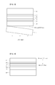
- FIGS. 1 to 5 are sectional views showing a light emitting device and a method of manufacturing the same according to the embodiment.
- each layer shown in the drawings may be exaggerated, omitted or schematically drawn for the purpose of convenience or clarity.
- the size of elements does not utterly reflect an actual size.
- FIGS. 1 to 5 are sectional views showing a light emitting device and a method of manufacturing the same according to the embodiment.
- a light emitting semiconductor layer including a first conductive semiconductor layer 20, an active layer 30, and a second conductive semiconductor layer 40 is formed on a growth substrate 10, and a current spreading layer 50 and a first wafer bonding layer 60 are formed on the second conductive semiconductor layer 40.
- the growth substrate 10 may include one selected from the group consisting of Al 2 O 3 , SiC, Si, AlN, GaN, AlGaN, glass, and GaAs.
- a buffer layer may be formed between the growth substrate 10 and the first conductive semiconductor layer 20.
- the buffer layer is formed on the growth substrate 10 to improve lattice match between the growth substrate 10 and the first conductive semiconductor layer 20.
- the buffer layer may include at least one selected from the group consisting of InGaN, AlN, SiC, SiCN, and GaN.
- the light emitting semiconductor layer may be formed on the buffer layer through single crystal growth schemes such as MOCVD and MBE.
- the first conductive semiconductor layer 20 may include a GaN layer or an AlGaN layer doped with Si, Ge, Se, or Te.
- the active layer 30 may include an undoped InGaN layer and an undoped GaN layer, and the second conductive semiconductor layer 40 may include a GaN layer or an AlGaN layer doped with Mg, Zn, Ca, Sr, or Ba.
- the light emitting semiconductor layer has a surface having a nitrogen polarity in opposition to the growth substrate 10, and has a surface having a metallic polarity in opposition to the current spreading layer 50.
- the current spreading layer 50 may include a material, such as Al, Ag, or Rh, representing 70% or more of a reflectance in a wavelength band of 600nm or less.
- the current spreading layer 50 forms an ohmic contacting interface with respect to the second conductive semiconductor layer 40, so that current can be easily injected in a vertical direction.
- the first wafer bonding layer 60 is formed on the current spreading layer 50, and may include a material, such as Au, Ag, Cu, Pt, Pd, or Al, representing superior thermal conductivity and strong mechanical bonding strength.
- a superlattice structure layer may be formed between the second conductive semiconductor layer 40 and the current spreading layer 50.
- the superlattice structure layer forms an ohmic contacting interface with respect to the second conductive semiconductor layer 40 so that current can be easily injected in a vertical direction.
- the superlattice structure layer may increase the effective concentration of holes by reducing dopant activation energy of the second conducive semiconductor layer 40, or may cause a quantum mechanical tunneling conductivity through band-gap engineering.
- the superlattice structure layer may have a multi-layer structure including a nitride or a carbon nitride including group II, III, or IV elements. Each layer constituting the superlattice structure layer may have a thickness of about 5nm or less. Each layer constituting the superlattice structure layer may include at least one selected from the group consisting of InN, InGaN, InAlN, AlGaN, GaN, AlInGaN, AlN, SiC, SiCN, MgN, ZnN, and SiN, and may be doped with Si, Mg, or Zn.
- the superlattice structure layer may have a multi-layer structure such as InGaN/GaN, AlGaN/GaN, InGaN/GaN/AlGaN, or AlGaN/GaN/InGaN.
- the superlattice structure layer may have a single layer structure.
- the superlattice structure layer may include an InGaN layer, a GaN layer, an AlInN layer, an AlN layer, an InN layer, an AlGaN layer, or an AlInGaN layer doped with N type impurities, or may include an InGaN layer, a GaN layer, an AlInN layer, an AlN layer, an InN layer, an AlGaN layer, or an AlInGaN layer doped with P type impurities.
- a support substrate 80 having a second wafer bonding layer 70 is bonded to an upper portion of the first wafer bonding layer 60.
- the second wafer bonding layer 70 is formed on the support substrate 80, and then bonded to the first wafer bonding layer 60.
- the second wafer bonding layer 70 may be omitted, or the support substrate 80 may be directly bonded on the upper portion of the first wafer bonding layer 60.
- the second wafer bonding layer 70 may include a material, such as Au, Ag, Cu, Pt, Pd, Al, representing superior thermal conductivity and strong mechanical bonding strength.
- the support substrate 80 may include at least one selected from the group consisting of Al 2 O 3 , SiC, Si, GaAs, Cu, Ni, NiCu, NiCr, Nb, Au, Ta, Ti, and metallic silicide.
- the growth substrate 10 is separated from the structure of FIG. 2 .
- the first conductive semiconductor layer 20 is exposed to the outside.
- the surface having a nitrogen polarity that is, a nitrogen (N)-face of the first conductive semiconductor layer 20 is exposed.
- a surface modification layer 90 is formed on the first conductive semiconductor layer 20 having the exposed surface of the nitrogen polarity, and a first electrode layer 100 is formed on the surface modification layer 90.
- the surface modification layer 90 and the first electrode layer 100 are formed on the whole surface of the first conductive semiconductor layer 20 as shown in FIG. 5 , the surface modification layer 90 and the first electrode layer 100 may be partially formed on the first conductive semiconductor layer 20
- the surface modification layer 90 is formed on the surface having the nitrogen polarity of the first conductive semiconductor layer 20, so that the first electrode layer 100 may form an ohmic contacting interface.
- the surface modification layer 90 may include a metallic compound having a thickness of 5nm or less.
- the metallic compound may include the compound of at least one selected from the group consisting of S, Se, Te, and F and at least one selected from the group consisting of In, Mg, Al, Ga, and La.
- the surface modification layer 90 includes In 2 S 3
- the first electrode layer 100 may have a stack structure of ITO/Cr/Al/Ni/Au.
- the surface modification layer 90 may include a metallic compound including Ga elements.
- the metallic compound may include one selected from the group consisting of Gallium-oxide, Ga-S, Ga-Se, andGa-Te.
- the surface modification layer 90 includes Ga 2 O 3
- the first electrode layer 100 may have a stack structure of ITO/Cr/Al/Ni/Au.
- the surface modification layer 90 may include metal having an atomic radius greater than that of Ga, or may include the alloy or the solid solution including the metal having an atomic radius greater than that of Ga.
- the metal having an atomic radius greater than that of Ga may include Ge, Y, Zr, Nb, Mo, Fe, Tc, Ru, Rh, Pd, Ag, Cd, In, Sn, Sb, Lu, Hf, Ta, W, Re, Os, Ir, Pt, Au, Bi, or La-based metal.
- the surface modification layer 90 may include Rh (Rhodium), and the first electrode layer 100 may have the stack structure of Cr/Al/Ni/Au.
- the surface modification layer 90 and the first electrode layer 100 may be formed through E-beam deposition, PVD (physical vapor deposition), CVD (chemical vapor deposition), PLD (plasma laser deposition), dual-type thermal evaporator, or sputtering.
- the surface modification layer 90 and the first electrode layer 100 may be formed under a condition of the temperature of about 20°C to about 1500°C and an atmosphere pressure to a pressure of 10 -12 torr.
- a heat treatment process can be performed in a chamber.
- the heat treatment process may be performed under a condition of a temperature of about 100°C to about 800°C and a vacuum or gas atmosphere for 10 seconds to three hours.
- the gas introduced into the chamber may include at least one of nitrogen, argon, helium, oxygen, hydrogen, and air.
- the light emitting device according to the embodiment can be manufactured.
- the surface modification layer 90 is formed on the first conductive semiconductor layer 20 having a nitrogen polarity, so that a superior ohmic contacting interface can be formed. Accordingly, the electrical characteristic of the light emitting device can be improved.
- the embodiment is applicable to a light emitting device used as a light source.
Landscapes
- Led Devices (AREA)
Applications Claiming Priority (4)
| Application Number | Priority Date | Filing Date | Title |
|---|---|---|---|
| KR20080041105A KR20090115322A (ko) | 2008-05-02 | 2008-05-02 | 그룹 3족 질화물계 반도체 소자 |
| KR1020080041097A KR101459770B1 (ko) | 2008-05-02 | 2008-05-02 | 그룹 3족 질화물계 반도체 소자 |
| KR20080041102A KR20090115319A (ko) | 2008-05-02 | 2008-05-02 | 그룹 3족 질화물계 반도체 소자 |
| PCT/KR2009/002352 WO2009134109A2 (ko) | 2008-05-02 | 2009-05-04 | 발광 소자 및 그 제조방법 |
Publications (3)
| Publication Number | Publication Date |
|---|---|
| EP2290708A2 true EP2290708A2 (de) | 2011-03-02 |
| EP2290708A4 EP2290708A4 (de) | 2012-11-28 |
| EP2290708B1 EP2290708B1 (de) | 2015-09-02 |
Family
ID=41255584
Family Applications (1)
| Application Number | Title | Priority Date | Filing Date |
|---|---|---|---|
| EP09739015.7A Not-in-force EP2290708B1 (de) | 2008-05-02 | 2009-05-04 | Leuchtelement und herstellungsverfahren dafür |
Country Status (4)
| Country | Link |
|---|---|
| US (1) | US9059338B2 (de) |
| EP (1) | EP2290708B1 (de) |
| CN (1) | CN102017203B (de) |
| WO (1) | WO2009134109A2 (de) |
Families Citing this family (5)
| Publication number | Priority date | Publication date | Assignee | Title |
|---|---|---|---|---|
| CN103579428B (zh) * | 2012-07-30 | 2016-08-17 | 比亚迪股份有限公司 | 一种led外延片及其制备方法 |
| WO2020175971A1 (ko) | 2019-02-28 | 2020-09-03 | 안상정 | 고순도 압전 박막 및 이 박막을 이용하는 소자를 제조하는 방법 |
| CN110379895B (zh) * | 2019-07-25 | 2022-04-22 | 湘能华磊光电股份有限公司 | Led外延生长方法 |
| CN112320838B (zh) * | 2019-08-05 | 2022-09-06 | Tcl科技集团股份有限公司 | 纳米材料及其制备方法和应用 |
| CN114823999B (zh) * | 2022-06-24 | 2023-02-28 | 江西兆驰半导体有限公司 | 一种具有氮极性接触层的led外延结构及其制备方法 |
Family Cites Families (12)
| Publication number | Priority date | Publication date | Assignee | Title |
|---|---|---|---|---|
| JP3680558B2 (ja) * | 1998-05-25 | 2005-08-10 | 日亜化学工業株式会社 | 窒化物半導体素子 |
| KR100589621B1 (ko) * | 1998-03-12 | 2006-06-19 | 니치아 카가쿠 고교 가부시키가이샤 | 질화물 반도체 소자 |
| KR20010000545A (ko) * | 2000-10-05 | 2001-01-05 | 유태경 | 펌핑 층이 집적된 다 파장 AlGaInN계 반도체LED 소자 및 그 제조 방법 |
| JP2002329877A (ja) * | 2001-04-27 | 2002-11-15 | National Institute Of Advanced Industrial & Technology | Cu(Ga及び(又は)In)Se2薄膜層、Cu(InGa)(S、Se)2薄膜層、太陽電池、Cu(Ga及び(又は)In)Se2薄膜層の形成方法 |
| JP4055053B2 (ja) * | 2002-03-26 | 2008-03-05 | 本田技研工業株式会社 | 化合物薄膜太陽電池およびその製造方法 |
| KR101030068B1 (ko) * | 2002-07-08 | 2011-04-19 | 니치아 카가쿠 고교 가부시키가이샤 | 질화물 반도체 소자의 제조방법 및 질화물 반도체 소자 |
| KR100543696B1 (ko) * | 2002-09-09 | 2006-01-20 | 삼성전기주식회사 | 고효율 발광 다이오드 |
| GB2432970B (en) | 2004-08-31 | 2008-03-05 | Sumitomo Chemical Co | Compound semiconductor luminescent device |
| KR100706952B1 (ko) * | 2005-07-22 | 2007-04-12 | 삼성전기주식회사 | 수직 구조 질화갈륨계 발광다이오드 소자 및 그 제조방법 |
| KR100635157B1 (ko) * | 2005-09-09 | 2006-10-17 | 삼성전기주식회사 | 질화물계 반도체 발광소자 |
| CN100375303C (zh) * | 2005-10-27 | 2008-03-12 | 晶能光电(江西)有限公司 | 含有金锗镍的欧姆电极、铟镓铝氮半导体发光元件及制造方法 |
| KR100815225B1 (ko) * | 2006-10-23 | 2008-03-19 | 삼성전기주식회사 | 수직구조 발광다이오드 소자 및 그 제조방법 |
-
2009
- 2009-05-04 US US12/990,398 patent/US9059338B2/en active Active
- 2009-05-04 WO PCT/KR2009/002352 patent/WO2009134109A2/ko not_active Ceased
- 2009-05-04 CN CN200980115885.7A patent/CN102017203B/zh not_active Expired - Fee Related
- 2009-05-04 EP EP09739015.7A patent/EP2290708B1/de not_active Not-in-force
Also Published As
| Publication number | Publication date |
|---|---|
| CN102017203B (zh) | 2013-04-10 |
| WO2009134109A2 (ko) | 2009-11-05 |
| EP2290708A4 (de) | 2012-11-28 |
| US9059338B2 (en) | 2015-06-16 |
| CN102017203A (zh) | 2011-04-13 |
| EP2290708B1 (de) | 2015-09-02 |
| US20110163294A1 (en) | 2011-07-07 |
| WO2009134109A3 (ko) | 2010-02-25 |
Similar Documents
| Publication | Publication Date | Title |
|---|---|---|
| US8502193B2 (en) | Light-emitting device and fabricating method thereof | |
| US8829554B2 (en) | Light emitting element and a production method therefor | |
| US7521269B2 (en) | Single-crystal nitride-based semiconductor substrate and method of manufacturing high-quality nitride-based light emitting device by using the same | |
| US8471239B2 (en) | Light-emitting element and a production method therefor | |
| US8021904B2 (en) | Ohmic contacts to nitrogen polarity GaN | |
| TWI430477B (zh) | 具有大面積及高能量之高效率第iii族氮化物為基礎之頂部發光型發光裝置及其製造方法 | |
| US7795050B2 (en) | Single-crystal nitride-based semiconductor substrate and method of manufacturing high-quality nitride-based light emitting device by using the same | |
| CN104576861B (zh) | 半导体缓冲结构、半导体器件以及制造半导体器件的方法 | |
| US20080303055A1 (en) | Group-III Nitride-Based Light Emitting Device | |
| KR101257572B1 (ko) | 반도체 발광 소자 | |
| US8633508B2 (en) | Semiconductor element and a production method therefor | |
| KR101047617B1 (ko) | 반도체 발광소자 및 그 제조방법 | |
| US20070145396A1 (en) | Semiconductor light emitting device and method of manufacturing the same | |
| JP2003060212A (ja) | シヨットキバリアダイオード及びその製造方法 | |
| US9059338B2 (en) | Light emitting element and a production method therefor | |
| KR101064068B1 (ko) | 발광소자의 제조방법 | |
| KR20090115322A (ko) | 그룹 3족 질화물계 반도체 소자 | |
| US20080248639A1 (en) | Method for forming electrode for group III nitride based compound semiconductor and method for manufacturing p-type group III nitride based compound semiconductor | |
| KR100832102B1 (ko) | 발광소자용 구조체 및 발광소자의 제조 방법 | |
| WO2005117151A1 (en) | Positive electrode structure and gallium nitride-based compound semiconductor light-emitting device | |
| CN110473943B (zh) | 发光二极管元件、以及发光二极管元件的制造方法 | |
| KR101459770B1 (ko) | 그룹 3족 질화물계 반도체 소자 | |
| KR101045949B1 (ko) | 질화물 반도체 발광소자 및 이의 제조 방법 | |
| KR101026059B1 (ko) | 질화물 반도체 발광소자 및 그 제조방법 | |
| KR100513349B1 (ko) | 질화물 반도체 발광소자 및 그 제조방법 |
Legal Events
| Date | Code | Title | Description |
|---|---|---|---|
| PUAI | Public reference made under article 153(3) epc to a published international application that has entered the european phase |
Free format text: ORIGINAL CODE: 0009012 |
|
| 17P | Request for examination filed |
Effective date: 20101130 |
|
| AK | Designated contracting states |
Kind code of ref document: A2 Designated state(s): AT BE BG CH CY CZ DE DK EE ES FI FR GB GR HR HU IE IS IT LI LT LU LV MC MK MT NL NO PL PT RO SE SI SK TR |
|
| AX | Request for extension of the european patent |
Extension state: AL BA RS |
|
| DAX | Request for extension of the european patent (deleted) | ||
| A4 | Supplementary search report drawn up and despatched |
Effective date: 20121031 |
|
| RIC1 | Information provided on ipc code assigned before grant |
Ipc: H01L 33/02 20100101ALN20121025BHEP Ipc: H01L 33/14 20100101AFI20121025BHEP |
|
| 17Q | First examination report despatched |
Effective date: 20131106 |
|
| REG | Reference to a national code |
Ref country code: DE Ref legal event code: R079 Ref document number: 602009033340 Country of ref document: DE Free format text: PREVIOUS MAIN CLASS: H01L0033000000 Ipc: H01L0033140000 |
|
| GRAP | Despatch of communication of intention to grant a patent |
Free format text: ORIGINAL CODE: EPIDOSNIGR1 |
|
| INTG | Intention to grant announced |
Effective date: 20150416 |
|
| RIC1 | Information provided on ipc code assigned before grant |
Ipc: H01L 33/02 20100101ALN20150408BHEP Ipc: H01L 33/14 20100101AFI20150408BHEP |
|
| GRAS | Grant fee paid |
Free format text: ORIGINAL CODE: EPIDOSNIGR3 |
|
| GRAA | (expected) grant |
Free format text: ORIGINAL CODE: 0009210 |
|
| AK | Designated contracting states |
Kind code of ref document: B1 Designated state(s): AT BE BG CH CY CZ DE DK EE ES FI FR GB GR HR HU IE IS IT LI LT LU LV MC MK MT NL NO PL PT RO SE SI SK TR |
|
| REG | Reference to a national code |
Ref country code: GB Ref legal event code: FG4D |
|
| REG | Reference to a national code |
Ref country code: AT Ref legal event code: REF Ref document number: 747104 Country of ref document: AT Kind code of ref document: T Effective date: 20150915 Ref country code: CH Ref legal event code: EP |
|
| REG | Reference to a national code |
Ref country code: IE Ref legal event code: FG4D |
|
| REG | Reference to a national code |
Ref country code: DE Ref legal event code: R096 Ref document number: 602009033340 Country of ref document: DE |
|
| REG | Reference to a national code |
Ref country code: AT Ref legal event code: MK05 Ref document number: 747104 Country of ref document: AT Kind code of ref document: T Effective date: 20150902 |
|
| PG25 | Lapsed in a contracting state [announced via postgrant information from national office to epo] |
Ref country code: FI Free format text: LAPSE BECAUSE OF FAILURE TO SUBMIT A TRANSLATION OF THE DESCRIPTION OR TO PAY THE FEE WITHIN THE PRESCRIBED TIME-LIMIT Effective date: 20150902 Ref country code: NO Free format text: LAPSE BECAUSE OF FAILURE TO SUBMIT A TRANSLATION OF THE DESCRIPTION OR TO PAY THE FEE WITHIN THE PRESCRIBED TIME-LIMIT Effective date: 20151202 Ref country code: GR Free format text: LAPSE BECAUSE OF FAILURE TO SUBMIT A TRANSLATION OF THE DESCRIPTION OR TO PAY THE FEE WITHIN THE PRESCRIBED TIME-LIMIT Effective date: 20151203 Ref country code: LT Free format text: LAPSE BECAUSE OF FAILURE TO SUBMIT A TRANSLATION OF THE DESCRIPTION OR TO PAY THE FEE WITHIN THE PRESCRIBED TIME-LIMIT Effective date: 20150902 Ref country code: LV Free format text: LAPSE BECAUSE OF FAILURE TO SUBMIT A TRANSLATION OF THE DESCRIPTION OR TO PAY THE FEE WITHIN THE PRESCRIBED TIME-LIMIT Effective date: 20150902 |
|
| REG | Reference to a national code |
Ref country code: LT Ref legal event code: MG4D Ref country code: NL Ref legal event code: MP Effective date: 20150902 |
|
| PG25 | Lapsed in a contracting state [announced via postgrant information from national office to epo] |
Ref country code: ES Free format text: LAPSE BECAUSE OF FAILURE TO SUBMIT A TRANSLATION OF THE DESCRIPTION OR TO PAY THE FEE WITHIN THE PRESCRIBED TIME-LIMIT Effective date: 20150902 Ref country code: AT Free format text: LAPSE BECAUSE OF FAILURE TO SUBMIT A TRANSLATION OF THE DESCRIPTION OR TO PAY THE FEE WITHIN THE PRESCRIBED TIME-LIMIT Effective date: 20150902 Ref country code: SE Free format text: LAPSE BECAUSE OF FAILURE TO SUBMIT A TRANSLATION OF THE DESCRIPTION OR TO PAY THE FEE WITHIN THE PRESCRIBED TIME-LIMIT Effective date: 20150902 Ref country code: PL Free format text: LAPSE BECAUSE OF FAILURE TO SUBMIT A TRANSLATION OF THE DESCRIPTION OR TO PAY THE FEE WITHIN THE PRESCRIBED TIME-LIMIT Effective date: 20150902 |
|
| PG25 | Lapsed in a contracting state [announced via postgrant information from national office to epo] |
Ref country code: IS Free format text: LAPSE BECAUSE OF FAILURE TO SUBMIT A TRANSLATION OF THE DESCRIPTION OR TO PAY THE FEE WITHIN THE PRESCRIBED TIME-LIMIT Effective date: 20160102 Ref country code: EE Free format text: LAPSE BECAUSE OF FAILURE TO SUBMIT A TRANSLATION OF THE DESCRIPTION OR TO PAY THE FEE WITHIN THE PRESCRIBED TIME-LIMIT Effective date: 20150902 Ref country code: SK Free format text: LAPSE BECAUSE OF FAILURE TO SUBMIT A TRANSLATION OF THE DESCRIPTION OR TO PAY THE FEE WITHIN THE PRESCRIBED TIME-LIMIT Effective date: 20150902 Ref country code: IT Free format text: LAPSE BECAUSE OF FAILURE TO SUBMIT A TRANSLATION OF THE DESCRIPTION OR TO PAY THE FEE WITHIN THE PRESCRIBED TIME-LIMIT Effective date: 20150902 Ref country code: NL Free format text: LAPSE BECAUSE OF FAILURE TO SUBMIT A TRANSLATION OF THE DESCRIPTION OR TO PAY THE FEE WITHIN THE PRESCRIBED TIME-LIMIT Effective date: 20150902 Ref country code: CZ Free format text: LAPSE BECAUSE OF FAILURE TO SUBMIT A TRANSLATION OF THE DESCRIPTION OR TO PAY THE FEE WITHIN THE PRESCRIBED TIME-LIMIT Effective date: 20150902 |
|
| PG25 | Lapsed in a contracting state [announced via postgrant information from national office to epo] |
Ref country code: PT Free format text: LAPSE BECAUSE OF FAILURE TO SUBMIT A TRANSLATION OF THE DESCRIPTION OR TO PAY THE FEE WITHIN THE PRESCRIBED TIME-LIMIT Effective date: 20160104 Ref country code: RO Free format text: LAPSE BECAUSE OF FAILURE TO SUBMIT A TRANSLATION OF THE DESCRIPTION OR TO PAY THE FEE WITHIN THE PRESCRIBED TIME-LIMIT Effective date: 20150902 |
|
| REG | Reference to a national code |
Ref country code: DE Ref legal event code: R097 Ref document number: 602009033340 Country of ref document: DE |
|
| PLBE | No opposition filed within time limit |
Free format text: ORIGINAL CODE: 0009261 |
|
| STAA | Information on the status of an ep patent application or granted ep patent |
Free format text: STATUS: NO OPPOSITION FILED WITHIN TIME LIMIT |
|
| 26N | No opposition filed |
Effective date: 20160603 |
|
| PG25 | Lapsed in a contracting state [announced via postgrant information from national office to epo] |
Ref country code: DK Free format text: LAPSE BECAUSE OF FAILURE TO SUBMIT A TRANSLATION OF THE DESCRIPTION OR TO PAY THE FEE WITHIN THE PRESCRIBED TIME-LIMIT Effective date: 20150902 Ref country code: SI Free format text: LAPSE BECAUSE OF FAILURE TO SUBMIT A TRANSLATION OF THE DESCRIPTION OR TO PAY THE FEE WITHIN THE PRESCRIBED TIME-LIMIT Effective date: 20150902 Ref country code: BE Free format text: LAPSE BECAUSE OF NON-PAYMENT OF DUE FEES Effective date: 20160531 |
|
| PG25 | Lapsed in a contracting state [announced via postgrant information from national office to epo] |
Ref country code: LU Free format text: LAPSE BECAUSE OF FAILURE TO SUBMIT A TRANSLATION OF THE DESCRIPTION OR TO PAY THE FEE WITHIN THE PRESCRIBED TIME-LIMIT Effective date: 20160504 Ref country code: BE Free format text: LAPSE BECAUSE OF FAILURE TO SUBMIT A TRANSLATION OF THE DESCRIPTION OR TO PAY THE FEE WITHIN THE PRESCRIBED TIME-LIMIT Effective date: 20150902 |
|
| REG | Reference to a national code |
Ref country code: CH Ref legal event code: PL |
|
| PG25 | Lapsed in a contracting state [announced via postgrant information from national office to epo] |
Ref country code: LI Free format text: LAPSE BECAUSE OF NON-PAYMENT OF DUE FEES Effective date: 20160531 Ref country code: CH Free format text: LAPSE BECAUSE OF NON-PAYMENT OF DUE FEES Effective date: 20160531 |
|
| REG | Reference to a national code |
Ref country code: IE Ref legal event code: MM4A |
|
| REG | Reference to a national code |
Ref country code: FR Ref legal event code: ST Effective date: 20170131 |
|
| PG25 | Lapsed in a contracting state [announced via postgrant information from national office to epo] |
Ref country code: FR Free format text: LAPSE BECAUSE OF NON-PAYMENT OF DUE FEES Effective date: 20160531 |
|
| PG25 | Lapsed in a contracting state [announced via postgrant information from national office to epo] |
Ref country code: IE Free format text: LAPSE BECAUSE OF NON-PAYMENT OF DUE FEES Effective date: 20160504 |
|
| PG25 | Lapsed in a contracting state [announced via postgrant information from national office to epo] |
Ref country code: HU Free format text: LAPSE BECAUSE OF FAILURE TO SUBMIT A TRANSLATION OF THE DESCRIPTION OR TO PAY THE FEE WITHIN THE PRESCRIBED TIME-LIMIT; INVALID AB INITIO Effective date: 20090504 Ref country code: CY Free format text: LAPSE BECAUSE OF FAILURE TO SUBMIT A TRANSLATION OF THE DESCRIPTION OR TO PAY THE FEE WITHIN THE PRESCRIBED TIME-LIMIT Effective date: 20150902 |
|
| PG25 | Lapsed in a contracting state [announced via postgrant information from national office to epo] |
Ref country code: MK Free format text: LAPSE BECAUSE OF FAILURE TO SUBMIT A TRANSLATION OF THE DESCRIPTION OR TO PAY THE FEE WITHIN THE PRESCRIBED TIME-LIMIT Effective date: 20150902 Ref country code: MT Free format text: LAPSE BECAUSE OF NON-PAYMENT OF DUE FEES Effective date: 20160531 Ref country code: TR Free format text: LAPSE BECAUSE OF FAILURE TO SUBMIT A TRANSLATION OF THE DESCRIPTION OR TO PAY THE FEE WITHIN THE PRESCRIBED TIME-LIMIT Effective date: 20150902 Ref country code: HR Free format text: LAPSE BECAUSE OF FAILURE TO SUBMIT A TRANSLATION OF THE DESCRIPTION OR TO PAY THE FEE WITHIN THE PRESCRIBED TIME-LIMIT Effective date: 20150902 Ref country code: MC Free format text: LAPSE BECAUSE OF FAILURE TO SUBMIT A TRANSLATION OF THE DESCRIPTION OR TO PAY THE FEE WITHIN THE PRESCRIBED TIME-LIMIT Effective date: 20150902 |
|
| PG25 | Lapsed in a contracting state [announced via postgrant information from national office to epo] |
Ref country code: BG Free format text: LAPSE BECAUSE OF FAILURE TO SUBMIT A TRANSLATION OF THE DESCRIPTION OR TO PAY THE FEE WITHIN THE PRESCRIBED TIME-LIMIT Effective date: 20150902 |
|
| REG | Reference to a national code |
Ref country code: GB Ref legal event code: 732E Free format text: REGISTERED BETWEEN 20210722 AND 20210728 |
|
| REG | Reference to a national code |
Ref country code: DE Ref legal event code: R081 Ref document number: 602009033340 Country of ref document: DE Owner name: SUZHOU LEKIN SEMICONDUCTOR CO. LTD., TAICANG, CN Free format text: FORMER OWNER: LG INNOTEK CO., LTD, SEOUL, KR |
|
| PGFP | Annual fee paid to national office [announced via postgrant information from national office to epo] |
Ref country code: DE Payment date: 20230404 Year of fee payment: 15 |
|
| PGFP | Annual fee paid to national office [announced via postgrant information from national office to epo] |
Ref country code: GB Payment date: 20230406 Year of fee payment: 15 |
|
| REG | Reference to a national code |
Ref country code: DE Ref legal event code: R079 Ref document number: 602009033340 Country of ref document: DE Free format text: PREVIOUS MAIN CLASS: H01L0033140000 Ipc: H10H0020816000 |
|
| REG | Reference to a national code |
Ref country code: DE Ref legal event code: R119 Ref document number: 602009033340 Country of ref document: DE |
|
| GBPC | Gb: european patent ceased through non-payment of renewal fee |
Effective date: 20240504 |
|
| PG25 | Lapsed in a contracting state [announced via postgrant information from national office to epo] |
Ref country code: DE Free format text: LAPSE BECAUSE OF NON-PAYMENT OF DUE FEES Effective date: 20241203 |
|
| PG25 | Lapsed in a contracting state [announced via postgrant information from national office to epo] |
Ref country code: GB Free format text: LAPSE BECAUSE OF NON-PAYMENT OF DUE FEES Effective date: 20240504 |