EP2290677A2 - Method for evaluating semiconductor device - Google Patents
Method for evaluating semiconductor device Download PDFInfo
- Publication number
- EP2290677A2 EP2290677A2 EP10172478A EP10172478A EP2290677A2 EP 2290677 A2 EP2290677 A2 EP 2290677A2 EP 10172478 A EP10172478 A EP 10172478A EP 10172478 A EP10172478 A EP 10172478A EP 2290677 A2 EP2290677 A2 EP 2290677A2
- Authority
- EP
- European Patent Office
- Prior art keywords
- semiconductor
- semiconductor substrate
- sheet
- electrode
- test
- Prior art date
- Legal status (The legal status is an assumption and is not a legal conclusion. Google has not performed a legal analysis and makes no representation as to the accuracy of the status listed.)
- Withdrawn
Links
Images



Classifications
-
- H—ELECTRICITY
- H10—SEMICONDUCTOR DEVICES; ELECTRIC SOLID-STATE DEVICES NOT OTHERWISE PROVIDED FOR
- H10P—GENERIC PROCESSES OR APPARATUS FOR THE MANUFACTURE OR TREATMENT OF DEVICES COVERED BY CLASS H10
- H10P74/00—Testing or measuring during manufacture or treatment of wafers, substrates or devices
- H10P74/23—Testing or measuring during manufacture or treatment of wafers, substrates or devices characterised by multiple measurements, corrections, marking or sorting processes
-
- H—ELECTRICITY
- H10—SEMICONDUCTOR DEVICES; ELECTRIC SOLID-STATE DEVICES NOT OTHERWISE PROVIDED FOR
- H10P—GENERIC PROCESSES OR APPARATUS FOR THE MANUFACTURE OR TREATMENT OF DEVICES COVERED BY CLASS H10
- H10P74/00—Testing or measuring during manufacture or treatment of wafers, substrates or devices
- H10P74/20—Testing or measuring during manufacture or treatment of wafers, substrates or devices characterised by the properties tested or measured, e.g. structural or electrical properties
- H10P74/207—Electrical properties, e.g. testing or measuring of resistance, deep levels or capacitance-voltage characteristics
-
- G—PHYSICS
- G01—MEASURING; TESTING
- G01R—MEASURING ELECTRIC VARIABLES; MEASURING MAGNETIC VARIABLES
- G01R31/00—Arrangements for testing electric properties; Arrangements for locating electric faults; Arrangements for electrical testing characterised by what is being tested not provided for elsewhere
- G01R31/28—Testing of electronic circuits, e.g. by signal tracer
- G01R31/282—Testing of electronic circuits specially adapted for particular applications not provided for elsewhere
- G01R31/2831—Testing of materials or semi-finished products, e.g. semiconductor wafers or substrates
Definitions
- the embodiment discussed herein is related to a method for evaluating a semiconductor device and, more particularly, to a semiconductor device evaluation method of a vertical semiconductor device.
- a plurality of semiconductor devices are arranged longitudinally and laterally. These semiconductor devices are divided by dicing and then, incorporated into a semiconductor module.
- FIG. 5 is a configuration view of an apparatus for performing the electrical characteristic test.
- FIG. 5 illustrates a state of a static characteristic test for measuring a leakage current between electrodes on vertical semiconductor devices.
- a prober (test apparatus) 100 includes a cantilever type probe pin 101, a probe card 102 for supporting the probe pin 101, and a prober stage 104 for supporting a semiconductor substrate 103 as an object to be inspected.
- a plurality of vertical semiconductor devices are arranged in every direction of the semiconductor substrate 103.
- each vertical semiconductor device On each vertical semiconductor device, a surface structure and a rear surface electrode are formed. On the surface structure, a gate electrode and an emitter electrode are formed. Further, the rear surface electrode serves as a collector electrode, and is configured by a metal film.
- the prober stage 104 When the prober stage 104 is raised, a plurality of probe pins 101 having needlepoints with different diameters contact electrodes on the surface structure, and the vertical semiconductor device with a contacted portion is subjected to the static characteristic test. Further, when a relative position between the probe pin 101 and the semiconductor substrate 103 is changed, the plurality of vertical semiconductor devices are continuously subjected to the static characteristic test on the same stage.
- FIG. 6 illustrates a relationship between a voltage and current applied to the vertical semiconductor device.
- the horizontal axis of FIG. 6 represents the time, and illustrates the variation per hour of a voltage and current in the case where a short circuit occurs in an IGBT (Insulated Gate Bipolar Transistor) device during a turn-off operation of the high current switching test.
- IGBT Insulated Gate Bipolar Transistor
- FIG. 6 illustrates a state where when the short circuit occurs, a switching operation of the IGBT device is disabled.
- a fissure may grow up in a radial pattern from a crack without staying on a portion in which this crack occurs.
- the dynamic characteristic test is not generally performed in a wafer state due to the fact that fissures grow up in a radial pattern in the dynamic characteristic test of the vertical semiconductor device.
- the reason is that when the dynamic characteristic test is performed in the wafer state, the fissure may grow up to a nondefective vertical semiconductor device adjacent to a defective vertical semiconductor device and therefore, the nondefective vertical semiconductor device receives the damage.
- the fact is that a simple body of a semiconductor chip is subjected to the dynamic characteristic test.
- the dynamic characteristic test after the semiconductor substrate is divided into the semiconductor chips by dicing, the individual semiconductor chips are moved up to a prober using a chip handler and a simple body of the semiconductor chip is subjected to the dynamic characteristic test. Therefore, a continuous test fails to be performed on the same stage and therefore, inspection efficiency is reduced.
- this method includes: fixing a sheet having electrical conductivity to a main surface of a semiconductor substrate on which a plurality of semiconductor devices having a surface structure and a rear surface electrode are arranged; dividing the semiconductor substrate into semiconductor chips on a first support stage in the state where the sheet is fixed to the main surface; and mounting the plurality of divided semiconductor chips on a second support stage via the sheet, and continuously subjecting the plurality of mounted semiconductor chips to a dynamic characteristic test on the second support stage.
- FIG. 1 is a flowchart illustrating a fundamental principle of a semiconductor device evaluation method.
- a plurality of vertical semiconductor devices are first fabricated within a semiconductor substrate in a wafer processing (step S1). On surfaces of these vertical semiconductor devices, gate electrodes each functioning as a control electrode and emitter (source) electrodes each functioning as a main electrode are formed. On rear surfaces of the vertical semiconductor devices, rear surface electrodes each functioning as a collector (drain) electrode are formed. For example, an IGBT device or power MOSFET (Metal Oxide Semiconductor Field Effect Transistor) falls under this vertical semiconductor device.
- MOSFET Metal Oxide Semiconductor Field Effect Transistor
- step S2 a sheet having electrical conductivity is fixed to rear surface electrodes of all the vertical semiconductor devices formed in the semiconductor substrate. This processing permits a rear surface of the semiconductor substrate to be protected by the sheet having electrical conductivity.
- the semiconductor substrate is divided by dicing with the sheet being fixed to the rear surface of the semiconductor substrate (step S3).
- This processing permits vertical semiconductor chips to be made into individual pieces from the semiconductor substrate.
- a plurality of vertical semiconductor chips that are made into individual pieces from the semiconductor substrate are continuously subjected to a dynamic characteristic test via the sheet on a testing support stage (step S4). For example, a high current switching test falls under the dynamic characteristic test.
- the sheet is separated from the rear surface electrode of the semiconductor chip and the semiconductor chip that is determined to be a nondefective chip in the dynamic characteristic test is incorporated into a semiconductor module.
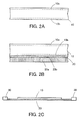
- FIGS. 2A and 2B are schematic sectional views illustrating essential parts of a processing of laminating a dicing tape to the semiconductor substrate having formed therein the vertical semiconductor devices.
- FIG. 2A illustrates the semiconductor substrate before laminating the dicing tape thereto
- FIGS. 2B and 2C illustrate the semiconductor substrate after laminating the dicing tape thereto.
- the semiconductor substrate 10 illustrated in FIG. 2A is a plate-shaped wafer composed mainly of silicon (Si) and, for example, an epitaxial growth substrate or FZ (Floating Zone) substrate falls under the semiconductor substrate 10.
- a thickness of the semiconductor substrate 10 is, for example, 0.5 mm or less.
- the semiconductor substrate 10 has a surface structure 10a and a rear surface electrode 10b.
- the semiconductor substrate 10 is subjected to a wafer processing, and on the surface layer of the semiconductor substrate 10, for example, the control electrode (gate electrode) of the vertical semiconductor device or the emitter electrode (source electrode) as one main electrode of the vertical semiconductor device is formed.
- the collector electrode (drain electrode) as another main electrode is formed.
- the rear surface electrode 10b is configured by a metal multilayered film composed of, for example, aluminum (Al), titanium (Ti), nickel (Ni), and gold (Au).
- the plurality of vertical semiconductor devices each including the surface structure 10a and the rear surface electrode 10b are arranged longitudinally and laterally on the semiconductor substrate 10. As described above, the IGBT device or power MOSFET falls under the vertical semiconductor device.
- the dicing tape 20 is laminated on the rear surface side of the semiconductor substrate 10. More specifically, an alignment between the semiconductor substrate 10 in which a wafer processing is completed and the dicing tape 20 having an area larger than that of the semiconductor substrate 10 is performed.
- the dicing tape 20 is laminated to the rear surface electrodes 10b of the vertical semiconductor devices formed in the semiconductor substrate 10. This processing permits the dicing tape 20 to be fixed to the rear surface electrode 10b of the vertical semiconductor device, and a rear surface of the semiconductor substrate 10 to be protected by the dicing tape 20.
- the dicing tape 20 is a sheet having elasticity and adhesion composed of a resin layer 20a being a base member and an adhesive member 20b formed over the resin layer 20a.
- the resin layer 20a and the adhesive member 20b include a metal powder (not illustrated) such as copper (Cu), gold (Au), and aluminum (A1).
- An electric resistance of the dicing tape 20 including the above-described metal powder is maintained in the range of the same electric resistance as that of metal such as copper (Cu), gold (Au), and aluminum (Al).
- a high current of approximately 0 to 300 amperes energized in the vertical semiconductor device is stably energized in the thickness direction (vertical direction) and in-plane direction of the dicing tape 20.
- the adhesive member 20b of the dicing tape 20 has quality that its adhesion is reduced at a predetermined temperature (e.g., 100 to 150°C) and separation is easily performed in an interface between the adhesive member 20b and the rear surface electrode 10b.
- a predetermined temperature e.g. 100 to 150°C
- a ring-shaped dicing frame 30 is provided on the end of the dicing tape 20. After fixing the semiconductor substrate 10 to the dicing tape 20, the semiconductor substrate 10, the dicing tape 20, and the dicing frame 30 can be collectively moved by a manual transport or automating transport.
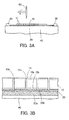
- FIGS. 3A and 3B are schematic sectional views illustrating essential parts of a dicing processing.
- FIG. 3A illustrates the whole view
- FIG. 3B illustrates an enlarged view.
- the semiconductor substrate 10, the dicing tape 20, and the dicing frame 30 are mounted on a dicing table 40 serving as a dicing support stage, thus fixing the dicing tape 20 and the dicing frame 30. Further, a relative position between a dicing blade 50 and the semiconductor substrate 10 is changed in every direction while rotating the dicing blade 50 at a predetermined rotating speed and bringing the dicing blade 50 into contact with the semiconductor substrate 10. Further, the semiconductor substrate 10 on the dicing tape 20 is divided at a predetermined interval and the vertical semiconductor chips 11 are made into individual pieces from the semiconductor substrate 10.
- a cut 10c is made in the semiconductor substrate 10 using the dicing blade 50 until perfectly separating the semiconductor substrate 10 into the individual vertical semiconductor chips 11.
- the cut 10c is stopped at a position of the interface between the semiconductor substrate 10 and the dicing tape 20. Or alternatively, as illustrated in FIG. 3B , the cut 10c is stopped at a position where it is slightly penetrated in the thickness direction of the dicing tape 20 from the interface between the semiconductor substrate 10 and the dicing tape 20.
- the dicing tape 20 is prevented from being divided and only the semiconductor substrate 10 on the dicing tape 20 is divided into the individual vertical semiconductor chips 11.
- water may be fed to a cut section using a feed-water unit while the semiconductor substrate 10 is divided using the dicing blade 50
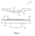
- FIG. 4 is a schematic sectional view illustrating an essential part of the high current switching test processing.
- a prober (test apparatus) 60 is configured by a prober stage 61 as a testing support stage, a probe card 62, and a plurality of cantilever type probe pins 63 attached onto the probe card 62. Strength of the probe pin 63 is reinforced using a supporting material 64.
- the plurality of vertical semiconductor chips 11 divided in the previous step, the dicing tape 20, and the dicing frame 30 are mounted on the prober stage 61 and further, the dicing tape 20 and the dicing frame 30 are fixed to the prober stage 61.
- the rear surface electrodes 10b of the individual vertical semiconductor chips 11 and the prober stage 61 are electrically conductive to each other via the dicing tape 20, and the plurality of vertical semiconductor chips are arranged on the same prober stage 61.
- the probe pin 63 is brought into contact with the emitter electrode or gate electrode (not illustrated) on the vertical semiconductor chips 11 that are made into individual pieces from the semiconductor substrate, and the individual vertical semiconductor chips 11 are continuously subjected to the high current switching test on the same prober stage 61.
- any one of the plurality of probe pins 63 is brought into contact with the emitter electrode or gate electrode of at least one of the vertical semiconductor chips 11 arranged on the prober stage 61, and then a voltage is applied between the emitter electrode and the rear surface electrode 10b. Further, when a pulse voltage is applied to the gate electrode, a state of its gate is set to a turn-on state or turn-off state (switching). A high current of approximately 0 to several hundred amperes is energized or disconnected between the emitter electrode and the rear surface electrode 10b. For example, a current up to 500 amperes is energized or disconnected by switching.
- the dicing tape 20 having electrical conductivity is disposed between the rear surface electrode 10b and the prober stage 61. Therefore, an energizing path between the rear surface electrode of the vertical semiconductor chip 11 and the prober stage 61 is secured via the dicing tape 20. Accordingly, the above-described high current switching test can be stably performed on the prober stage 61. Further, after a test for one vertical semiconductor chip is completed, a test for another vertical semiconductor chip adjacent to the semiconductor chip is moved.
- the high current switching tests for all the vertical semiconductor chips on the prober stage 61 are completed.
- a plurality of probe pins 63 are collectively brought into contact with a plurality of electrodes of the vertical semiconductor chips 11 and the high current switching test may be performed.
- the static characteristic test for measuring a leakage current between the gate electrode and the emitter electrode may be performed, if desired.
- the dicing tape 20 is transported to, for example, a heating plate or warming device in order to heat the dicing tape 20 to approximately 100 to 150°C (not illustrated).
- the above-described processing enables adhesion of the adhesive member 20b of the dicing tape 20 to be weakened and the dicing tape 20 to be simply separated from the rear surface electrode 10b.
- the vertical semiconductor chip 11 determined to be a defective chip in the above-described testing processing is removed from a manufacturing processing. Further, these defective semiconductor chips are not allowed to move to the next process. On the other hand, the vertical semiconductor chip 11 in which a crack does not occur in a device is allowed to move to the next process and further, incorporated into a semiconductor module by performing the packaging operation.
- the proposed semiconductor device evaluation method of the present invention permits the plurality of vertical semiconductor chips to be continuously subjected to the high current switching test on the same prober stage 61 in the state where the plurality of vertical semiconductor chips are fixed to the dicing tape 20. As a result, the inspection efficiency is significantly improved.
- the individual divided vertical semiconductor chips 11 are subjected independently to the high current switching test. Therefore, a fissure growing up from a crack that occurs in a defective semiconductor chip is prevented from propagating over other adjacent semiconductor chips. This processing permits the number of the nondefective vertical semiconductor chips 11 per the semiconductor substrate 10 to increase, and the yield and productivity of the semiconductor module to be improved.
- the dynamic characteristic test is described as the dynamic characteristic test and the dynamic characteristic test is not limited to the high-current switching test.
- the present embodiment can be applied to, for example, a reverse bias safe operating area (RBSOA) test, a turning-off test, an avalanche test, and a load short-circuit test.
- RSOA reverse bias safe operating area
- an example of a current of 500 amperes for performing energization and disconnection is cited, and further, the present embodiment can be applied also to a test for higher current (e.g., 1200 amperes).
- the sheet having electrical conductivity is fixed to a main surface of the semiconductor substrate on which the plurality of semiconductor devices having a surface structure and a rear surface electrode are arranged.
- the semiconductor substrate is divided into the semiconductor chips on a first support stage in the state where the sheet is fixed to its main surface.
- the plurality of divided semiconductor chips are mounted on a second support stage via the sheet and further, the plurality of mounted semiconductor chips are continuously subjected to the dynamic characteristic test on the second support stage.
- the proposed semiconductor device evaluation method permits a fissure growing and propagating from a crack occurring in the dynamic characteristic test of the vertical semiconductor device to be suppressed, and the yield and productivity of the semiconductor module to be improved.
Landscapes
- Testing Or Measuring Of Semiconductors Or The Like (AREA)
- Testing Of Individual Semiconductor Devices (AREA)
Abstract
Description
- The embodiment discussed herein is related to a method for evaluating a semiconductor device and, more particularly, to a semiconductor device evaluation method of a vertical semiconductor device.
- On a semiconductor substrate that is subjected to a wafer processing, a plurality of semiconductor devices are arranged longitudinally and laterally. These semiconductor devices are divided by dicing and then, incorporated into a semiconductor module.
- The above-described semiconductor devices are normally subjected, before being incorporated into the semiconductor module, to an electrical characteristic test for the semiconductor device. For example,
FIG. 5 is a configuration view of an apparatus for performing the electrical characteristic test. -
FIG. 5 illustrates a state of a static characteristic test for measuring a leakage current between electrodes on vertical semiconductor devices. - A prober (test apparatus) 100 includes a cantilever
type probe pin 101, aprobe card 102 for supporting theprobe pin 101, and aprober stage 104 for supporting asemiconductor substrate 103 as an object to be inspected. Here, as described above, a plurality of vertical semiconductor devices (not illustrated) are arranged in every direction of thesemiconductor substrate 103. - On each vertical semiconductor device, a surface structure and a rear surface electrode are formed. On the surface structure, a gate electrode and an emitter electrode are formed. Further, the rear surface electrode serves as a collector electrode, and is configured by a metal film.
- When the
prober stage 104 is raised, a plurality ofprobe pins 101 having needlepoints with different diameters contact electrodes on the surface structure, and the vertical semiconductor device with a contacted portion is subjected to the static characteristic test. Further, when a relative position between theprobe pin 101 and thesemiconductor substrate 103 is changed, the plurality of vertical semiconductor devices are continuously subjected to the static characteristic test on the same stage. - On the other hand, in the electrical characteristic test, a dynamic characteristic test as in a so-called high current switching test is performed in addition to the static characteristic test.
- However, in the dynamic characteristic test, a high current of approximately 0 to several hundred amperes is energized within the vertical semiconductor device. Therefore, cracks with a diameter of approximately 100 µm may occur in the defective vertical semiconductor device. For example,
FIG. 6 illustrates a relationship between a voltage and current applied to the vertical semiconductor device. - The horizontal axis of
FIG. 6 represents the time, and illustrates the variation per hour of a voltage and current in the case where a short circuit occurs in an IGBT (Insulated Gate Bipolar Transistor) device during a turn-off operation of the high current switching test. - As illustrated in
FIG. 6 , when the turn-off operation is started, a voltage (VCE) between collector and emitter electrodes instantaneously rises up and a collector current (IC) falls down. However, after the short circuit occurs at the time of occurrence of cracks illustrated inFIG. 6 , the voltage (VCE) between the collector and emitter electrodes falls down and the collector current (IC) rises up. In other words,FIG. 6 illustrates a state where when the short circuit occurs, a switching operation of the IGBT device is disabled. - Further, in damage within the vertical semiconductor device, a fissure may grow up in a radial pattern from a crack without staying on a portion in which this crack occurs.
- As described above, the dynamic characteristic test is not generally performed in a wafer state due to the fact that fissures grow up in a radial pattern in the dynamic characteristic test of the vertical semiconductor device. The reason is that when the dynamic characteristic test is performed in the wafer state, the fissure may grow up to a nondefective vertical semiconductor device adjacent to a defective vertical semiconductor device and therefore, the nondefective vertical semiconductor device receives the damage.
- Accordingly, the fact is that a simple body of a semiconductor chip is subjected to the dynamic characteristic test. As a result, there arises the following problem. That is, in the dynamic characteristic test, after the semiconductor substrate is divided into the semiconductor chips by dicing, the individual semiconductor chips are moved up to a prober using a chip handler and a simple body of the semiconductor chip is subjected to the dynamic characteristic test. Therefore, a continuous test fails to be performed on the same stage and therefore, inspection efficiency is reduced.
- There is disclosed a method for continuously subjecting a plurality of semiconductor chips to an electrical characteristic test on the same stage without moving the semiconductor chips up to a test apparatus by a chip handler after dividing the semiconductor substrate by dicing (for example, Japanese Laid-open Patent Publication No.
2003-258067 - However, in the above-described known example, a displacement of the semiconductor chips on a support stage, which occurs after the dicing is merely prevented. Accordingly, when cracks that occur in the above-described dynamic characteristic test grow or propagate in a radial pattern, the known example does not prevent the damage from being further expanded. That is, the above-described problem at the time of performing the dynamic characteristic test of the vertical semiconductor device is not yet solved.
- In view of the foregoing, it is an object of the present invention to provide a method for evaluating a semiconductor device for suppressing a fissure growing up or propagating over from a crack occurring in a dynamic characteristic test of a vertical semiconductor device and improving a yield of a semiconductor module. According to one aspect of the present invention, this method includes: fixing a sheet having electrical conductivity to a main surface of a semiconductor substrate on which a plurality of semiconductor devices having a surface structure and a rear surface electrode are arranged; dividing the semiconductor substrate into semiconductor chips on a first support stage in the state where the sheet is fixed to the main surface; and mounting the plurality of divided semiconductor chips on a second support stage via the sheet, and continuously subjecting the plurality of mounted semiconductor chips to a dynamic characteristic test on the second support stage.
-
-
FIG. 1 is a flowchart illustrating a fundamental principle of a method for evaluating a semiconductor device; -
FIGS. 2A to 2C are schematic sectional views illustrating an essential part of a processing of laminating a dicing tape to a semiconductor substrate on which vertical semiconductor devices are formed; -
FIGS. 3A and 3B are schematic sectional views illustrating an essential part of a dicing processing; -
FIG. 4 is a schematic sectional view illustrating an essential part of a high current switching test processing; -
FIG. 5 is a configuration view of an apparatus for performing an electrical characteristic test; and -
FIG. 6 illustrates a relationship between a voltage and current applied to the vertical semiconductor device. - A preferred embodiment of the present invention will now be described in detail below with reference to the accompanying drawings, wherein like reference numerals refer to like elements throughout. At first, a fundamental principle of a method for evaluating a semiconductor device according to the present invention will be described.
-
FIG. 1 is a flowchart illustrating a fundamental principle of a semiconductor device evaluation method. - A plurality of vertical semiconductor devices are first fabricated within a semiconductor substrate in a wafer processing (step S1). On surfaces of these vertical semiconductor devices, gate electrodes each functioning as a control electrode and emitter (source) electrodes each functioning as a main electrode are formed. On rear surfaces of the vertical semiconductor devices, rear surface electrodes each functioning as a collector (drain) electrode are formed. For example, an IGBT device or power MOSFET (Metal Oxide Semiconductor Field Effect Transistor) falls under this vertical semiconductor device.
- Next, a sheet having electrical conductivity is fixed to rear surface electrodes of all the vertical semiconductor devices formed in the semiconductor substrate (step S2). This processing permits a rear surface of the semiconductor substrate to be protected by the sheet having electrical conductivity.
- Next, the semiconductor substrate is divided by dicing with the sheet being fixed to the rear surface of the semiconductor substrate (step S3). This processing permits vertical semiconductor chips to be made into individual pieces from the semiconductor substrate.
- A plurality of vertical semiconductor chips that are made into individual pieces from the semiconductor substrate are continuously subjected to a dynamic characteristic test via the sheet on a testing support stage (step S4). For example, a high current switching test falls under the dynamic characteristic test.
- Thereafter, the sheet is separated from the rear surface electrode of the semiconductor chip and the semiconductor chip that is determined to be a nondefective chip in the dynamic characteristic test is incorporated into a semiconductor module.
- Next, a specific method of the semiconductor device evaluation method will be described based on a flowchart of
FIG. 1 . -
FIGS. 2A and 2B are schematic sectional views illustrating essential parts of a processing of laminating a dicing tape to the semiconductor substrate having formed therein the vertical semiconductor devices. Here,FIG. 2A illustrates the semiconductor substrate before laminating the dicing tape thereto, andFIGS. 2B and 2C illustrate the semiconductor substrate after laminating the dicing tape thereto. - The
semiconductor substrate 10 illustrated inFIG. 2A is a plate-shaped wafer composed mainly of silicon (Si) and, for example, an epitaxial growth substrate or FZ (Floating Zone) substrate falls under thesemiconductor substrate 10. A thickness of thesemiconductor substrate 10 is, for example, 0.5 mm or less. Further, thesemiconductor substrate 10 has asurface structure 10a and arear surface electrode 10b. Specifically, thesemiconductor substrate 10 is subjected to a wafer processing, and on the surface layer of thesemiconductor substrate 10, for example, the control electrode (gate electrode) of the vertical semiconductor device or the emitter electrode (source electrode) as one main electrode of the vertical semiconductor device is formed. On the other hand, on a rear surface layer of thesemiconductor substrate 10, the collector electrode (drain electrode) as another main electrode is formed. In addition, therear surface electrode 10b is configured by a metal multilayered film composed of, for example, aluminum (Al), titanium (Ti), nickel (Ni), and gold (Au). - As can be seen from the above discussion, the plurality of vertical semiconductor devices each including the
surface structure 10a and therear surface electrode 10b are arranged longitudinally and laterally on thesemiconductor substrate 10. As described above, the IGBT device or power MOSFET falls under the vertical semiconductor device. - Next, as illustrated in
FIG. 2B , the dicingtape 20 is laminated on the rear surface side of thesemiconductor substrate 10. More specifically, an alignment between thesemiconductor substrate 10 in which a wafer processing is completed and the dicingtape 20 having an area larger than that of thesemiconductor substrate 10 is performed. The dicingtape 20 is laminated to therear surface electrodes 10b of the vertical semiconductor devices formed in thesemiconductor substrate 10. This processing permits the dicingtape 20 to be fixed to therear surface electrode 10b of the vertical semiconductor device, and a rear surface of thesemiconductor substrate 10 to be protected by the dicingtape 20. - Here, the dicing
tape 20 is a sheet having elasticity and adhesion composed of aresin layer 20a being a base member and anadhesive member 20b formed over theresin layer 20a. Further, theresin layer 20a and theadhesive member 20b include a metal powder (not illustrated) such as copper (Cu), gold (Au), and aluminum (A1). An electric resistance of the dicingtape 20 including the above-described metal powder is maintained in the range of the same electric resistance as that of metal such as copper (Cu), gold (Au), and aluminum (Al). In the after-mentioned high current switching test, a high current of approximately 0 to 300 amperes energized in the vertical semiconductor device is stably energized in the thickness direction (vertical direction) and in-plane direction of the dicingtape 20. - As to flexibility of the in-plane direction and adhesion of the surface of the dicing
tape 20, it has quality comparable to those of known dicing tape. - Further, the
adhesive member 20b of the dicingtape 20 has quality that its adhesion is reduced at a predetermined temperature (e.g., 100 to 150°C) and separation is easily performed in an interface between theadhesive member 20b and therear surface electrode 10b. - As illustrated in
FIG. 2C , a ring-shapeddicing frame 30 is provided on the end of the dicingtape 20. After fixing thesemiconductor substrate 10 to the dicingtape 20, thesemiconductor substrate 10, the dicingtape 20, and thedicing frame 30 can be collectively moved by a manual transport or automating transport. -
FIGS. 3A and 3B are schematic sectional views illustrating essential parts of a dicing processing. Here,FIG. 3A illustrates the whole view, andFIG. 3B illustrates an enlarged view. - As illustrated in
FIG. 3A , thesemiconductor substrate 10, the dicingtape 20, and thedicing frame 30 are mounted on a dicing table 40 serving as a dicing support stage, thus fixing the dicingtape 20 and thedicing frame 30. Further, a relative position between a dicingblade 50 and thesemiconductor substrate 10 is changed in every direction while rotating thedicing blade 50 at a predetermined rotating speed and bringing thedicing blade 50 into contact with thesemiconductor substrate 10. Further, thesemiconductor substrate 10 on the dicingtape 20 is divided at a predetermined interval and thevertical semiconductor chips 11 are made into individual pieces from thesemiconductor substrate 10. - As illustrated in
FIG. 3B , acut 10c is made in thesemiconductor substrate 10 using thedicing blade 50 until perfectly separating thesemiconductor substrate 10 into the individualvertical semiconductor chips 11. - In relation to the dicing
tape 20, thecut 10c is stopped at a position of the interface between thesemiconductor substrate 10 and the dicingtape 20. Or alternatively, as illustrated inFIG. 3B , thecut 10c is stopped at a position where it is slightly penetrated in the thickness direction of the dicingtape 20 from the interface between thesemiconductor substrate 10 and the dicingtape 20. - As a result, the dicing
tape 20 is prevented from being divided and only thesemiconductor substrate 10 on the dicingtape 20 is divided into the individualvertical semiconductor chips 11. - For example, water may be fed to a cut section using a feed-water unit while the
semiconductor substrate 10 is divided using thedicing blade 50 -
FIG. 4 is a schematic sectional view illustrating an essential part of the high current switching test processing. - As illustrated in
FIG. 4 , a prober (test apparatus) 60 is configured by aprober stage 61 as a testing support stage, aprobe card 62, and a plurality of cantilever type probe pins 63 attached onto theprobe card 62. Strength of theprobe pin 63 is reinforced using a supportingmaterial 64. The plurality ofvertical semiconductor chips 11 divided in the previous step, the dicingtape 20, and thedicing frame 30 are mounted on theprober stage 61 and further, the dicingtape 20 and thedicing frame 30 are fixed to theprober stage 61. Under the above-described state, therear surface electrodes 10b of the individualvertical semiconductor chips 11 and theprober stage 61 are electrically conductive to each other via the dicingtape 20, and the plurality of vertical semiconductor chips are arranged on thesame prober stage 61. - Next, the
probe pin 63 is brought into contact with the emitter electrode or gate electrode (not illustrated) on thevertical semiconductor chips 11 that are made into individual pieces from the semiconductor substrate, and the individualvertical semiconductor chips 11 are continuously subjected to the high current switching test on thesame prober stage 61. - Specifically, any one of the plurality of probe pins 63 is brought into contact with the emitter electrode or gate electrode of at least one of the
vertical semiconductor chips 11 arranged on theprober stage 61, and then a voltage is applied between the emitter electrode and therear surface electrode 10b. Further, when a pulse voltage is applied to the gate electrode, a state of its gate is set to a turn-on state or turn-off state (switching). A high current of approximately 0 to several hundred amperes is energized or disconnected between the emitter electrode and therear surface electrode 10b. For example, a current up to 500 amperes is energized or disconnected by switching. - Here, as described above, the dicing
tape 20 having electrical conductivity is disposed between therear surface electrode 10b and theprober stage 61. Therefore, an energizing path between the rear surface electrode of thevertical semiconductor chip 11 and theprober stage 61 is secured via the dicingtape 20. Accordingly, the above-described high current switching test can be stably performed on theprober stage 61. Further, after a test for one vertical semiconductor chip is completed, a test for another vertical semiconductor chip adjacent to the semiconductor chip is moved. - By repeating the above-described test, the high current switching tests for all the vertical semiconductor chips on the
prober stage 61 are completed. Or alternatively, a plurality of probe pins 63 are collectively brought into contact with a plurality of electrodes of thevertical semiconductor chips 11 and the high current switching test may be performed. - Before performing the high current switching test, the static characteristic test for measuring a leakage current between the gate electrode and the emitter electrode may be performed, if desired.
- Next, the high current switching test for each semiconductor chip is completed and then, the dicing
tape 20 is transported to, for example, a heating plate or warming device in order to heat the dicingtape 20 to approximately 100 to 150°C (not illustrated). The above-described processing enables adhesion of theadhesive member 20b of the dicingtape 20 to be weakened and the dicingtape 20 to be simply separated from therear surface electrode 10b. Thevertical semiconductor chip 11 determined to be a defective chip in the above-described testing processing is removed from a manufacturing processing. Further, these defective semiconductor chips are not allowed to move to the next process. On the other hand, thevertical semiconductor chip 11 in which a crack does not occur in a device is allowed to move to the next process and further, incorporated into a semiconductor module by performing the packaging operation. - As can be seen from the above discussion, the proposed semiconductor device evaluation method of the present invention permits the plurality of vertical semiconductor chips to be continuously subjected to the high current switching test on the
same prober stage 61 in the state where the plurality of vertical semiconductor chips are fixed to the dicingtape 20. As a result, the inspection efficiency is significantly improved. - Further, according to the proposed semiconductor device evaluation method, the individual divided
vertical semiconductor chips 11 are subjected independently to the high current switching test. Therefore, a fissure growing up from a crack that occurs in a defective semiconductor chip is prevented from propagating over other adjacent semiconductor chips. This processing permits the number of the nondefectivevertical semiconductor chips 11 per thesemiconductor substrate 10 to increase, and the yield and productivity of the semiconductor module to be improved. - According to the present embodiment, one example of the high current switching test is described as the dynamic characteristic test and the dynamic characteristic test is not limited to the high-current switching test. Similarly, the present embodiment can be applied to, for example, a reverse bias safe operating area (RBSOA) test, a turning-off test, an avalanche test, and a load short-circuit test.
- According to the above-described embodiment, an example of a current of 500 amperes for performing energization and disconnection is cited, and further, the present embodiment can be applied also to a test for higher current (e.g., 1200 amperes).
- In the present invention, the sheet having electrical conductivity is fixed to a main surface of the semiconductor substrate on which the plurality of semiconductor devices having a surface structure and a rear surface electrode are arranged. The semiconductor substrate is divided into the semiconductor chips on a first support stage in the state where the sheet is fixed to its main surface. The plurality of divided semiconductor chips are mounted on a second support stage via the sheet and further, the plurality of mounted semiconductor chips are continuously subjected to the dynamic characteristic test on the second support stage.
- As can be seen from the present embodiment, the proposed semiconductor device evaluation method permits a fissure growing and propagating from a crack occurring in the dynamic characteristic test of the vertical semiconductor device to be suppressed, and the yield and productivity of the semiconductor module to be improved.
- All examples and conditional language recited herein are intended for pedagogical purposes to aid the reader in understanding the invention and the concepts contributed by the inventor to furthering the art, and are to be construed as being without limitation to such specifically recited examples and conditions, nor does the organization of such examples in the specification relate to a showing of the superiority and inferiority of the invention. Although the embodiment(s) of the present invention has(have) been described in detail, it should be understood that various changes, substitutions and alterations could be made hereto without departing from the spirit and scope of the invention.
Claims (3)
- A method for evaluating a semiconductor device, comprising:fixing a sheet having electrical conductivity to a main surface of a semiconductor substrate on which a plurality of semiconductor devices having a surface structure and a rear surface electrode are arranged;dividing the semiconductor substrate into semiconductor chips on a first support stage in the state where the sheet is fixed to the main surface; andmounting the plurality of divided semiconductor chips on a second support stage via the sheet, and continuously subjecting the plurality of mounted semiconductor chips to a dynamic characteristic test on the second support stage.
- The method according to claim 1, wherein:a main component of the sheet is composed of a resin and adhesive member including metal powder.
- The method according to claim 1 or 2, wherein:the dynamic characteristic test is a test for bringing a probe pin into contact with a control electrode or main electrode of at least one of the semiconductor devices that are mounted on the second support stage via the sheet, performing a continuous operation for turning on or off the control electrode, and energizing or disconnecting a current between the main electrode and the rear surface electrode.
Applications Claiming Priority (1)
| Application Number | Priority Date | Filing Date | Title |
|---|---|---|---|
| JP2009196182A JP2011047782A (en) | 2009-08-27 | 2009-08-27 | Method for evaluating semiconductor device |
Publications (2)
| Publication Number | Publication Date |
|---|---|
| EP2290677A2 true EP2290677A2 (en) | 2011-03-02 |
| EP2290677A3 EP2290677A3 (en) | 2012-11-21 |
Family
ID=43064333
Family Applications (1)
| Application Number | Title | Priority Date | Filing Date |
|---|---|---|---|
| EP10172478A Withdrawn EP2290677A3 (en) | 2009-08-27 | 2010-08-11 | Method for evaluating semiconductor device |
Country Status (4)
| Country | Link |
|---|---|
| US (1) | US8471585B2 (en) |
| EP (1) | EP2290677A3 (en) |
| JP (1) | JP2011047782A (en) |
| TW (1) | TWI555106B (en) |
Cited By (1)
| Publication number | Priority date | Publication date | Assignee | Title |
|---|---|---|---|---|
| CN103703381A (en) * | 2011-08-01 | 2014-04-02 | 东京毅力科创株式会社 | Probe card for power device |
Families Citing this family (6)
| Publication number | Priority date | Publication date | Assignee | Title |
|---|---|---|---|---|
| US9721853B2 (en) * | 2013-03-13 | 2017-08-01 | Taiwan Semiconductor Manufacturing Company, Ltd. | System and method for forming a semiconductor device |
| US10535572B2 (en) * | 2016-04-15 | 2020-01-14 | Taiwan Semiconductor Manufacturing Company, Ltd. | Device arrangement structure assembly and test method |
| JP6798418B2 (en) * | 2017-05-17 | 2020-12-09 | 三菱電機株式会社 | Manufacturing method of semiconductor devices |
| CN113805031B (en) * | 2021-11-19 | 2022-03-01 | 陕西开尔文测控技术有限公司 | Silicon carbide dynamic and static test all-in-one machine |
| US12270850B2 (en) * | 2023-03-08 | 2025-04-08 | Infineon Technologies Ag | Semiconductor device testing with lead extender |
| CN117110824B (en) * | 2023-10-23 | 2024-01-30 | 南京大学 | In-situ test system for semiconductor device |
Citations (2)
| Publication number | Priority date | Publication date | Assignee | Title |
|---|---|---|---|---|
| JP2003258067A (en) | 2002-03-04 | 2003-09-12 | Tokyo Electron Ltd | Dicing method, integrated circuit chip inspection method, and substrate holding device |
| US20070223156A1 (en) * | 2006-03-22 | 2007-09-27 | Tokyo Electron Limited | Circuit for protecting dut, method for protecting dut, testing apparatus and testing method |
Family Cites Families (15)
| Publication number | Priority date | Publication date | Assignee | Title |
|---|---|---|---|---|
| JPS58169921A (en) * | 1982-03-08 | 1983-10-06 | Hitachi Chem Co Ltd | Energizing inspection for p-n junction semiconductor element |
| JPH0465849A (en) * | 1990-07-06 | 1992-03-02 | Nec Kagoshima Ltd | Semiconductor pellet mounter |
| JPH06209042A (en) | 1993-01-12 | 1994-07-26 | Mitsubishi Electric Corp | Semiconductor wafer dicing tape and chip separation method |
| JPH07283173A (en) | 1994-04-13 | 1995-10-27 | Mitsumi Electric Co Ltd | Semiconductor wafer dicing equipment |
| JPH08194012A (en) | 1995-01-18 | 1996-07-30 | Fuji Electric Co Ltd | Semiconductor element characteristic measuring device |
| JPH11148961A (en) | 1997-09-11 | 1999-06-02 | Fuji Electric Co Ltd | Temperature measuring device for testing power semiconductor modules |
| US6525414B2 (en) * | 1997-09-16 | 2003-02-25 | Matsushita Electric Industrial Co., Ltd. | Semiconductor device including a wiring board and semiconductor elements mounted thereon |
| JP2000074988A (en) * | 1998-08-27 | 2000-03-14 | Fuji Electric Co Ltd | Method for manufacturing semiconductor device |
| JP2000074984A (en) | 1998-08-28 | 2000-03-14 | Meidensha Corp | Frequency test circuit of semiconductor element for electric power |
| US6400173B1 (en) * | 1999-11-19 | 2002-06-04 | Hitachi, Ltd. | Test system and manufacturing of semiconductor device |
| JP4564138B2 (en) * | 2000-07-10 | 2010-10-20 | Dowaホールディングス株式会社 | Manufacturing method of semiconductor device |
| JP2004071887A (en) | 2002-08-07 | 2004-03-04 | Renesas Technology Corp | Manufacturing method of vertical power semiconductor device |
| JP3535510B1 (en) | 2003-09-09 | 2004-06-07 | 尾池工業株式会社 | Transfer foil |
| JP2008071916A (en) | 2006-09-14 | 2008-03-27 | Fuji Electric Device Technology Co Ltd | Semiconductor device testing method |
| JP5055097B2 (en) | 2007-11-08 | 2012-10-24 | 日東電工株式会社 | Inspection adhesive sheet |
-
2009
- 2009-08-27 JP JP2009196182A patent/JP2011047782A/en active Pending
-
2010
- 2010-07-21 US US12/805,273 patent/US8471585B2/en active Active
- 2010-07-30 TW TW099125420A patent/TWI555106B/en not_active IP Right Cessation
- 2010-08-11 EP EP10172478A patent/EP2290677A3/en not_active Withdrawn
Patent Citations (2)
| Publication number | Priority date | Publication date | Assignee | Title |
|---|---|---|---|---|
| JP2003258067A (en) | 2002-03-04 | 2003-09-12 | Tokyo Electron Ltd | Dicing method, integrated circuit chip inspection method, and substrate holding device |
| US20070223156A1 (en) * | 2006-03-22 | 2007-09-27 | Tokyo Electron Limited | Circuit for protecting dut, method for protecting dut, testing apparatus and testing method |
Cited By (3)
| Publication number | Priority date | Publication date | Assignee | Title |
|---|---|---|---|---|
| CN103703381A (en) * | 2011-08-01 | 2014-04-02 | 东京毅力科创株式会社 | Probe card for power device |
| EP2762897A4 (en) * | 2011-08-01 | 2015-04-01 | Tokyo Electron Ltd | PROBE CARD FOR POWER SUPPLY DEVICE |
| US9322844B2 (en) | 2011-08-01 | 2016-04-26 | Tokyo Electron Limited | Probe card for power device |
Also Published As
| Publication number | Publication date |
|---|---|
| EP2290677A3 (en) | 2012-11-21 |
| JP2011047782A (en) | 2011-03-10 |
| TW201133672A (en) | 2011-10-01 |
| TWI555106B (en) | 2016-10-21 |
| US8471585B2 (en) | 2013-06-25 |
| US20110050269A1 (en) | 2011-03-03 |
Similar Documents
| Publication | Publication Date | Title |
|---|---|---|
| US8471585B2 (en) | Method for evaluating semiconductor device | |
| CN102713650B (en) | Probe apparatus | |
| CN109073705B (en) | Semiconductor test circuit, semiconductor test apparatus, and semiconductor test method | |
| EP2088441B1 (en) | Inspection device and inspection method | |
| JP5432700B2 (en) | Semiconductor device inspection equipment | |
| EP1788401B1 (en) | Method and apparatus for testing electrical characteristics of object under test | |
| CN112582290B (en) | Semiconductor testing device, testing method of semiconductor device, and manufacturing method of semiconductor device | |
| EP4018207B1 (en) | Safety system for needle probe card for high-voltage and high-current test on power semiconductor devices, related test machine and corresponding testing method | |
| EP2017634B1 (en) | Inspection apparatus and inspection method | |
| CN113690151B (en) | Method for manufacturing semiconductor device and method for manufacturing power control circuit | |
| KR101248439B1 (en) | Method of measuring characteristics of a semiconductor element and method of manufacturing a semiconductor device | |
| JP2011049337A (en) | Method of manufacturing semiconductor device | |
| US11307247B2 (en) | Prober with busbar mechanism for testing a device under test | |
| JPH10163281A (en) | Semiconductor device and method of manufacturing the same | |
| US9117880B2 (en) | Method for manufacturing semiconductor device | |
| KR101800521B1 (en) | Probe device | |
| US20180082882A1 (en) | Wafer Chuck, Use of the Wafer Chuck and Method for Testing a Semiconductor Wafer | |
| Rittner et al. | Robust top side contact technology on power semiconductors-results from the public funded projectpropower' | |
| JP2010108991A (en) | Element test method | |
| CN112444727A (en) | Wafer testing system and method | |
| US20230411200A1 (en) | Manufacturing method of semiconductor device, method of testing the semiconductor device and wafer holding member | |
| JP2004071887A (en) | Manufacturing method of vertical power semiconductor device | |
| JP2025038799A (en) | Semiconductor Manufacturing Equipment | |
| Buhrkal-Donau | Comparative study of wire bond degradation under power and mechanical cycling tests | |
| De La Cruz et al. | Failure analysis of power integrated modules and its challenges |
Legal Events
| Date | Code | Title | Description |
|---|---|---|---|
| PUAI | Public reference made under article 153(3) epc to a published international application that has entered the european phase |
Free format text: ORIGINAL CODE: 0009012 |
|
| AK | Designated contracting states |
Kind code of ref document: A2 Designated state(s): AL AT BE BG CH CY CZ DE DK EE ES FI FR GB GR HR HU IE IS IT LI LT LU LV MC MK MT NL NO PL PT RO SE SI SK SM TR |
|
| AX | Request for extension of the european patent |
Extension state: BA ME RS |
|
| RAP1 | Party data changed (applicant data changed or rights of an application transferred) |
Owner name: FUJI ELECTRIC CO., LTD. Owner name: TOKYO ELECTRON LIMITED |
|
| PUAL | Search report despatched |
Free format text: ORIGINAL CODE: 0009013 |
|
| AK | Designated contracting states |
Kind code of ref document: A3 Designated state(s): AL AT BE BG CH CY CZ DE DK EE ES FI FR GB GR HR HU IE IS IT LI LT LU LV MC MK MT NL NO PL PT RO SE SI SK SM TR |
|
| AX | Request for extension of the european patent |
Extension state: BA ME RS |
|
| RIC1 | Information provided on ipc code assigned before grant |
Ipc: H01L 21/66 20060101AFI20121019BHEP |
|
| 17P | Request for examination filed |
Effective date: 20130320 |
|
| 17Q | First examination report despatched |
Effective date: 20130626 |
|
| STAA | Information on the status of an ep patent application or granted ep patent |
Free format text: STATUS: THE APPLICATION IS DEEMED TO BE WITHDRAWN |
|
| 18D | Application deemed to be withdrawn |
Effective date: 20131107 |