EP2088441B1 - Inspection device and inspection method - Google Patents
Inspection device and inspection method Download PDFInfo
- Publication number
- EP2088441B1 EP2088441B1 EP07829980.7A EP07829980A EP2088441B1 EP 2088441 B1 EP2088441 B1 EP 2088441B1 EP 07829980 A EP07829980 A EP 07829980A EP 2088441 B1 EP2088441 B1 EP 2088441B1
- Authority
- EP
- European Patent Office
- Prior art keywords
- chip
- probe pin
- metal film
- top surface
- inspection
- Prior art date
- Legal status (The legal status is an assumption and is not a legal conclusion. Google has not performed a legal analysis and makes no representation as to the accuracy of the status listed.)
- Not-in-force
Links
Images


Classifications
-
- G—PHYSICS
- G01—MEASURING; TESTING
- G01R—MEASURING ELECTRIC VARIABLES; MEASURING MAGNETIC VARIABLES
- G01R1/00—Details of instruments or arrangements of the types included in groups G01R5/00 - G01R13/00 and G01R31/00
- G01R1/02—General constructional details
- G01R1/04—Housings; Supporting members; Arrangements of terminals
- G01R1/0408—Test fixtures or contact fields; Connectors or connecting adaptors; Test clips; Test sockets
Definitions
- the present invention relates to an inspection device and an inspecting method for inspecting electrical characteristics of a power device.
- the features of the preamble of claim 1 are known from EP 1 637 893 A1 .
- JP 2006 208 208 A discloses a related technology.
- a power device such as a power transistor, a power MOSFET (Metal-Oxide Semiconductor Field Effect Transistor), an IGBT (Insulated Gate Bipolar Transistor) or the like that has terminals on a top surface and a bottom surface thereof have been inspected by using a conventional inspection device.
- a power device such as a power transistor, a power MOSFET (Metal-Oxide Semiconductor Field Effect Transistor), an IGBT (Insulated Gate Bipolar Transistor) or the like that has terminals on a top surface and a bottom surface thereof have been inspected by using a conventional inspection device.
- MOSFET Metal-Oxide Semiconductor Field Effect Transistor
- IGBT Insulated Gate Bipolar Transistor
- the above-stated inspection device conventionally includes a chuck 100 for holding a substrate W of a power device, a probe card 102 disposed above the chuck 100 and supporting probe pins 101, and a tester 103 electrically connected with the probe card 102, as illustrated in Fig. 9 .
- the power device has terminals on a top surface and a bottom surface of the substrate W, so that formed on a substrate holding surface of the chuck 100 are inspection electrodes 104 electrically connected with the tester 103 through an internal wiring 105 formed within the chuck 100 (see Patent Document 1).
- Patent Document 1 Japanese Patent Laid-open Publication No. H6-242177
- the present invention has been conceived in view of the The present invention has been conceived in view of the foregoing, and an object of the present invention is to stably carry out a required inspection with a high accuracy when inspecting the electrical characteristics of the power device by forming the electric current path having a small load.
- an inspection device as defined in claim 1.
- the present invention by bringing one probe pin into contact with the top surface of the chip on the holding member for inspection and another probe pin into contact with the metal film on the surface of the holding member for inspection, it is possible to conduct the probe pins to the terminals on the top surface and the bottom surface of the power device. In this case, the electric current path formed during the inspection is shortened, so that a high resistance or inductance is not generated therein, thereby stably carrying out a desired inspection with a high accuracy.
- the positioning member may be a plurality of pins or protrusions in contact with a side surface of the chip.
- the positioning member may be a recessed portion capable of accommodating the chip and may be formed on the surface of the support plate, and the metal film may be formed in a range from a bottom surface of the recessed portion to an outer peripheral surface of an outside of the recessed portion.
- the positioning member may be a recessed portion capable of accommodating the chip and may be formed on a surface of the metal film.
- the holding member may further include a holding member another metal film insulated from the metal film and formed on the surface of the support plate in a range from an area on which the chip is mounted to an area on which the chip is not mounted.
- a suction opening for sucking and holding the chip may be formed in the area on which the chip is mounted on the surface the support plate.
- One or more suction opening may be formed, and the suction openings may be communicated with a common opening portion opened at a rear surface of the support plate.
- the support plate may mount thereon a plurality of chips, and the positioning member and the metal film may be formed for each chip.
- the inspection device may further include a top surface terminal fritting probe pin making a pair with the top surface terminal probe pin, which is in contact with the terminal on the top surface of the power device together with the top surface terminal probe pin and electrically conducts the top surface terminal probe pin to the terminal on the top surface by utilizing a fritting phenomenon; and a bottom surface terminal fritting probe pin making a pair with the bottom surface terminal probe pin, which is in contact with the metal film together with the bottom surface terminal probe pin and electrically conducts the bottom surface terminal probe pin to the metal film by utilizing a fritting phenomenon.
- an inspecting method for inspecting electrical characteristics of a power device by using an inspection device including: bringing, from a top surface side of the holding member for inspection, the top surface terminal probe pin into contact with the top surface of the chip on the holding member for inspection; bringing the bottom surface terminal probe pin into contact with the metal film; applying a voltage to the terminals on the top surface and the bottom surface of the power device; and inspecting the electrical characteristics.
- a bottom surface terminal fritting probe pin may be brought into contact with the terminal on the top surface of the power device together with the top surface terminal probe pin and the top surface terminal probe pin may be electrically conducted with the terminal on the top surface by utilizing a fritting phenomenon, and a bottom surface terminal fritting probe pin may be brought into contact with the metal film together with the bottom surface terminal probe pin and the bottom surface terminal probe pin may be electrically conducted with the metal film by utilizing a fritting phenomenon.
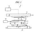
- FIG. 1 is an explanatory view schematically illustrating a structure of a probe device 1 serving as an inspection device in accordance with the present embodiment.
- the probe device 1 includes, for example, a probe card 2, a holding member 3 for inspection for holding chips C in which a power device is fabricated, a chuck 4 for adsorptively holding the holding member 3 for inspection, a moving mechanism 5 for moving the chuck 4, a tester 6 and the like.
- the probe card 2 includes, for example, a contactor 11 for supporting a plurality of probe pins 10 on its bottom surface and a printed circuit board 12 installed on a top surface of the contactor 11.
- the probe pins 10 are electrically connected with the printed circuit board 12 through a main body of the contactor 11.
- Electrically connected with the probe card 2 is the tester 6 from which electrical signals for inspecting electrical characteristics can be transceived to each of the probe pins 10 through the probe card 2.
- the chuck 4 is formed in an approximately disc shape having a flat top surface. Formed in the top surface of the chuck 4 is a suction opening 4a for adsorptively holding the holding member 3 for inspection.
- the suction opening 4a is connected with a suction line 4b which is connected with an external negative pressure generator 15, passing through the inside of the chuck 4, for example.
- the moving mechanism 5, as illustrated in Fig. 1 includes an elevation driving unit 20 such as a cylinder for elevating, e.g., the chuck 4 up and down and an X-Y stage 21 for moving the elevation driving unit 20 in both of the horizontal orthogonal X and Y directions, whereby the holding member 3 for inspection held on the chuck 4 can be three-dimensionally moved and a certain probe pin 10 disposed above can be brought into contact with a predetermined position on a surface of the holding member 3 for inspection.
- an elevation driving unit 20 such as a cylinder for elevating, e.g., the chuck 4 up and down and an X-Y stage 21 for moving the elevation driving unit 20 in both of the horizontal orthogonal X and Y directions, whereby the holding member 3 for inspection held on the chuck 4 can be three-dimensionally moved and a certain probe pin 10 disposed above can be brought into contact with a predetermined position on a surface of the holding member 3 for inspection.
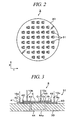
- the holding member 3 for inspection adsorptively held on the chuck 4 includes a support plate 30 having a thin disc shape with a thickness of about 1.5 mm and there is formed a plurality of chip mounting units 31 on a surface of the support plate 30 as illustrated in Fig. 2 , for example.
- the support plate 30 is made of, e.g., ceramic.
- the chip mounting units 31 are aligned on the surface of the support plate 30 in X and Y directions, for example.
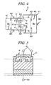
- the respective chip mounting units 31, as illustrated in Figs. 3 and 4 there are formed thin metal films 40 and 41 which are separated and insulated from each other.
- the metal films 40 and 41 are formed to have a multilayer structure composed of, e.g., copper, nickel, silver and gold and to have the same thickness of, e.g., about 0.1 mm.
- a first metal film 40 has an approximately quadrangle shape in a plane view as illustrated in Fig. 4 , and has a protruded portion 40a on its one surface at the side of a second metal film 41.
- the second metal film 41 as another metal film has an approximately quadrangle shape in a plane view and has a recessed portion 41a on its one surface at the side of the first metal film 40.
- the protruded portion 40a of the first metal film 40 and the recessed portion 41a of the second metal film 41 are formed to be engaged with each other.
- a chip C is mounted over from a part of the first metal film 40 to a part of the second metal film 41. That is, the first metal film 40 and the second metal film 41 are formed in a range from a mounting area R1, on which the chip C is mounted, to an exposed area R2 on which the chip C is not mounted, i.e., outside of the chip C.
- a plurality of pins 42 for positioning the chip C by being brought into contact with a side surface of the chip C is set up on each chip mounting table 31.
- the pins 42 are arranged along an outer periphery of the mounting area R1 on which the chip C is mounted.
- each chip mounting unit 31 formed in each chip mounting unit 31 is a plurality of suction openings 43.
- the suction openings 43 are formed in both of the first metal film 40 and the second metal film 41.
- Each of the suction openings 43 is communicated with a common bypass suction line 44 which is formed within the support plate 30 as illustrated in Fig. 3 , for example.
- the bypass suction line 44 is opened in a rear surface of the support plate 30 at a position corresponding to the suction opening 4a of the chuck 4 (opening portion 44a).
- the opening portion 44a of the bypass suction line 44 and the suction opening 4a in top surface of the chuck 4 are intercommunicated with each other, whereby the chip C is adsorptively held on the surface of the holding member 3 for inspection by a suction from the suction opening 4a of the chuck 4.
- a power device P in accordance with the present embodiment includes a top surface terminal C1 such as a gate, a source or an emitter on a top surface of the chip C and a bottom surface terminal C2 such as a drain or a collector on a bottom surface of the chip C as illustrated in Fig. 5 , for example.
- a plurality of chips C are mounted on the respective chip mounting units 31 of the holding member 3 for inspection as illustrated in Fig. 3 .
- the chip C is positioned by the pins 42 of each chip mounting unit 31.
- the holding member 3 for inspection is adsorptively held on the chuck 4 as illustrated in Fig. 1 .
- the chip C is sucked and fixed from the suction openings 43 of each chip mounting unit 31 by the sucking force of the chuck 4.
- the chuck 4 is moved by the moving mechanism 5 in a horizontal direction so as to adjust the position of the chip C in the X and Y directions and then the chuck 4 is elevated upward. In this manner, as illustrated in Fig.
- probe pins 10a and 10b are brought into contact with the top surface terminal C1 of the chip C and a probe pin 10c is brought into contact with a surface of the first metal film 40 in the exposed area R2 on which the chip C is not mounted. Further, a probe pin 10d is brought into contact with a surface of the second metal film 41 in the exposed area R2. Furthermore, in the present embodiment, the probe pin 10a serves as a probe pin for the top surface terminal and the probe pin 10c serves as a probe pin for the bottom surface terminal.
- a high voltage is applied between the probe pins 10a and 10c, for example, by the tester 6, an electric current flows from the probe pin 10a, the top surface terminal C1, the bottom surface terminal C2, the first metal film 40 and the probe pin 10c in sequence, and there is conducted, e.g., a withstand voltage test of the power device P.
- a voltage between the probe pin 10b and the probe pin 10d is measured by a non-illustrated monitor in the tester 6 so that a voltage actually applied onto the power device P during the inspection is measured.
- By measuring the actually applied voltage it is possible to apply an appropriate load to the device in consideration of electrical loss caused by a contact resistance. In this manner, electrical characteristics of the power device P are inspected by using a four-terminal Kelvin measurement method.
- the chuck 4 Upon completion of the inspection of electrical characteristics, the chuck 4 is elevated downward by the moving mechanism 5 and the respective probe pins 10 are spaced from the chip C. Thereafter, the holding member 3 for inspection is separated from the chuck 4 and a series of the inspection process is finished.
- the plurality of chip mounting units 31 is formed on the support plate 30 of the holding member 3 for inspection and on the surface of each chip mounting unit 31, the first metal film 40 is formed in a range from the mounting area R1, on which the chip C is mounted, to the exposed area R2 on which the chip C is not mounted.
- the pins 42 are formed on each chip mounting unit 31 so as to improve the positioning accuracy of the chip C, so that it is possible to carry out the inspection of the micro chip C with a high accuracy. Further, on the chip mounting unit 31, it may be possible to form protrusions made of resin or metal by a printing method or an etching method instead of the pins 42.
- each chip mounting unit 31 Formed on each chip mounting unit 31 is the second metal film 41 insulated from the first metal film 40, so that it is possible to bring one probe pin 10b into contact with the top surface terminal C1 of the chip C and another probe pin 10d into contact with the second metal film 41 in the exposed area R2 on which the chip C is not mounted during the inspection. In this manner, by measuring the voltage actually applied to the power device P, it can be checked that the inspection is appropriately carried out by the tester 6.
- the suction openings 43 are formed on each chip mounting unit 31, the chip C can be fixed onto the chip mounting unit 31. Further, the suction openings 43 are communicated with the common opening portion 44a in the rear surface of the support plate 30, so that the chip C can be adsorptively held onto the holding member 3 for inspection by suction from, e.g., the suction opening 4a of the chuck 4.
- the chip C is positioned by the pins 42, it may be also possible to form a recessed portion 30a capable of accommodating the chip C on the surface of the support plate 30 and to position the chip C by the recessed portion 30a, as illustrated in Fig. 6 .
- the recessed portion 30a having approximately the same shape as the chip C is formed in the mounting area R1 of the support plate 40, for example.
- the first and second metal films 40 and 41 are formed respectively in a range including a bottom surface of the recessed portion 30a, an inner side surface of the recessed portion 30a and an outer peripheral surface of the outside of the recessed portion 30a.
- a depth of the recessed portion 30a is set so that, for example, the top surface of the chip C accommodated in the recessed portion 30a is on the same plane with the outer peripheral surface of the outside of the recessed portion 30a.
- the chip C is accommodated in the recessed portion 30a, for example, the probe pins 10a and 10b are in contact with the top surface of the chip C; the probe pin 10c is in contact with the first metal film 40 in the outer peripheral surface of the recessed portion 30a; and the probe pin 10d is in contact with the second metal film 41 in the outer peripheral surface of the recessed portion 30a.
- the chip C is positioned at an appropriate position, thereby improving positional accuracy of the chip C, so that it is possible to carry out the inspection of the micro chip C with a high accuracy.
- a recessed portion 50 capable of accommodating the chip C on the surfaces of the first and second metal films 40 and 41.
- the recessed portion 50 is formed on a surface of the mounting area R1 of the first metal film 40 and the second metal film 41.
- the fritting phenomenon is such a phenomenon as follows. By applying a potential gradient of about 10 5 to 10 6 V/cm to a metal surface on which an oxide film is formed, the oxide film is broken down and a current flows in the metal surface.
- a test circuit 60 for transceiving electrical signals for inspecting electrical characteristics to or from the probe pins 10
- a fritting circuit 61 for applying a voltage to a pair of two probe pins 10 so as to generate the fritting phenomenon
- a switching circuit 62 for switching a connection between the test circuit 60 and the probe pins 10 to a connection between the fritting circuit 61 and the probe pins 10, for example.
- a pair of two probe pins 10a are in contact with the top surface terminal C1 of the chip C, for example; and another pair of two probe pins 10c are in contact with the first metal film 40 in the exposed area R2 of the outside of the chip C.
- the fritting circuit 61 applies a predetermined voltage between the pair of two probe pins 10a(10c), whereby the potential gradient between the pair of two probe pins 10a(10c) is increased.
- the fritting circuit 61 is switched to the test circuit 60 by the switching circuit 62; the voltage is applied between the top surface terminal C1 of the chip C and the first metal film 40 by, e.g., the two pairs of the probe pins 10a and 10c; and an inspection of electrical characteristics of the power device P is carried out in the same manner as in the above-stated embodiment.
- one of the probe pins 10a serves as a fritting probe pin for the top surface terminal and one of the probe pins 10c serves as a fritting probe pin for the bottom surface terminal.
- the probe pins 10 are electrically conducted with the top surface terminal C or with the first metal film 40 by utilizing the fritting phenomenon, so that it is not needed to heavily press down the probe pins 10 onto the top surface terminal C or the first metal film 40 and damage in the holding member 3 for inspection caused by such a press can be reduced.
- the holding member 3 for inspection can be used many times for a long time.
- the present invention is useful to an inspection of electrical characteristics of a power device when a required inspection should be stably carried out with a high accuracy by forming an electric current path having a small load.
Landscapes
- Physics & Mathematics (AREA)
- General Physics & Mathematics (AREA)
- Testing Of Individual Semiconductor Devices (AREA)
Description
- The present invention relates to an inspection device and an inspecting method for inspecting electrical characteristics of a power device. The features of the preamble of claim 1 are known from
EP 1 637 893 A1 .JP 2006 208 208 A - The electrical characteristics of a power device such as a power transistor, a power MOSFET (Metal-Oxide Semiconductor Field Effect Transistor), an IGBT (Insulated Gate Bipolar Transistor) or the like that has terminals on a top surface and a bottom surface thereof have been inspected by using a conventional inspection device.
- The above-stated inspection device conventionally includes a
chuck 100 for holding a substrate W of a power device, aprobe card 102 disposed above thechuck 100 and supporting probe pins 101, and atester 103 electrically connected with theprobe card 102, as illustrated inFig. 9 . The power device has terminals on a top surface and a bottom surface of the substrate W, so that formed on a substrate holding surface of thechuck 100 areinspection electrodes 104 electrically connected with thetester 103 through aninternal wiring 105 formed within the chuck 100 (see Patent Document 1). - In the inspection device, the electrical characteristics of the power device has been inspected by bring the probe pins 101 into contact with the terminal on the top surface of the power device, applying a voltage to the probe pins 101 and the
inspection electrodes 104 by thetester 103, and flowing an electric current through the power device.
Patent Document 1: Japanese Patent Laid-open Publication No.H6-242177 - However, in the above-stated inspection device, there is formed an electric current path from the
inspection electrodes 104 to thetester 103 through the inside of thechuck 100 when the inspection is carried out, so that the electric current path is lengthened and complicated, thereby generating a high resistance or inductance. For this reason, various loads impeding the electrical current are applied to the electrical current path while being electrically conducted during the inspection, so that it has been difficult to stably carry out the inspection with a desired accuracy. In particular, in case of flowing a great electric current through the power device to perform a reliability test, there is generated a higher resistance or inductance in the electric current path, whereby it has been difficult to appropriately carry out a required inspection. - The present invention has been conceived in view of the The present invention has been conceived in view of the foregoing, and an object of the present invention is to stably carry out a required inspection with a high accuracy when inspecting the electrical characteristics of the power device by forming the electric current path having a small load.
- In view of the foregoing, in accordance with one aspect of the present invention, there is provided an inspection device as defined in claim 1.
- In accordance with the present invention, by bringing one probe pin into contact with the top surface of the chip on the holding member for inspection and another probe pin into contact with the metal film on the surface of the holding member for inspection, it is possible to conduct the probe pins to the terminals on the top surface and the bottom surface of the power device. In this case, the electric current path formed during the inspection is shortened, so that a high resistance or inductance is not generated therein, thereby stably carrying out a desired inspection with a high accuracy.
- The positioning member may be a plurality of pins or protrusions in contact with a side surface of the chip.
- The positioning member may be a recessed portion capable of accommodating the chip and may be formed on the surface of the support plate, and the metal film may be formed in a range from a bottom surface of the recessed portion to an outer peripheral surface of an outside of the recessed portion.
- The positioning member may be a recessed portion capable of accommodating the chip and may be formed on a surface of the metal film.
- The holding member may further include a holding member another metal film insulated from the metal film and formed on the surface of the support plate in a range from an area on which the chip is mounted to an area on which the chip is not mounted.
- A suction opening for sucking and holding the chip may be formed in the area on which the chip is mounted on the surface the support plate.
- One or more suction opening may be formed, and the suction openings may be communicated with a common opening portion opened at a rear surface of the support plate.
- The support plate may mount thereon a plurality of chips, and the positioning member and the metal film may be formed for each chip.
- The inspection device may further include a top surface terminal fritting probe pin making a pair with the top surface terminal probe pin, which is in contact with the terminal on the top surface of the power device together with the top surface terminal probe pin and electrically conducts the top surface terminal probe pin to the terminal on the top surface by utilizing a fritting phenomenon; and a bottom surface terminal fritting probe pin making a pair with the bottom surface terminal probe pin, which is in contact with the metal film together with the bottom surface terminal probe pin and electrically conducts the bottom surface terminal probe pin to the metal film by utilizing a fritting phenomenon.
- In accordance with still another aspect of the present invention, there is provided an inspecting method for inspecting electrical characteristics of a power device by using an inspection device, the inspecting method including: bringing, from a top surface side of the holding member for inspection, the top surface terminal probe pin into contact with the top surface of the chip on the holding member for inspection; bringing the bottom surface terminal probe pin into contact with the metal film; applying a voltage to the terminals on the top surface and the bottom surface of the power device; and inspecting the electrical characteristics.
- A bottom surface terminal fritting probe pin may be brought into contact with the terminal on the top surface of the power device together with the top surface terminal probe pin and the top surface terminal probe pin may be electrically conducted with the terminal on the top surface by utilizing a fritting phenomenon, and a bottom surface terminal fritting probe pin may be brought into contact with the metal film together with the bottom surface terminal probe pin and the bottom surface terminal probe pin may be electrically conducted with the metal film by utilizing a fritting phenomenon.
- In accordance with the present invention, it is possible to stably carry out a required inspection with a high accuracy by forming an electric current path having a small electric load during the inspection.
-
-
Fig. 1 is a side view schematically illustrating a configuration of a probe device; -
Fig. 2 is a plane view of a holding member for inspection; -
Fig. 3 is an enlarged longitudinal cross section view showing a chip mounting unit of the holding member for inspection; -
Fig. 4 is an enlarged plane view showing the chip mounting unit of the holding member for inspection; -
Fig. 5 is an explanatory view showing an example of a configuration of a power device; -
Fig. 6 is an enlarged longitudinal cross section view of the chip mounting unit of the holding member for inspection in case of forming a recessed portion in a support plate; -
Fig. 7 is an enlarged longitudinal cross section view of the chip mounting unit of the holding member for inspection in case of forming a recessed portion in a metal film; -
Fig. 8 is an explanatory view illustrating a circuit configuration when utilizing a fritting phenomenon; and -
Fig. 9 is a schematic diagram showing a configuration of an inspection device of a conventional power device. -
- 1:
- probe device
- 2:
- probe card
- 3:
- holding member for inspection
- 4:
- chuck
- 6:
- tester
- 10:
- probe pins
- 30:
- support plate
- 40:
- first metal film
- 41:
- second metal film
- 42:
- pins
- 43:
- suction opening
- P:
- power device
- C:
- chip
- Hereinafter, desirable embodiments of the present invention will be explained.
Fig. 1 is an explanatory view schematically illustrating a structure of a probe device 1 serving as an inspection device in accordance with the present embodiment. - The probe device 1 includes, for example, a
probe card 2, a holdingmember 3 for inspection for holding chips C in which a power device is fabricated, a chuck 4 for adsorptively holding the holdingmember 3 for inspection, a movingmechanism 5 for moving the chuck 4, atester 6 and the like. - The
probe card 2 includes, for example, acontactor 11 for supporting a plurality of probe pins 10 on its bottom surface and a printedcircuit board 12 installed on a top surface of thecontactor 11. The probe pins 10 are electrically connected with the printedcircuit board 12 through a main body of thecontactor 11. Electrically connected with theprobe card 2 is thetester 6 from which electrical signals for inspecting electrical characteristics can be transceived to each of the probe pins 10 through theprobe card 2. - The chuck 4 is formed in an approximately disc shape having a flat top surface. Formed in the top surface of the chuck 4 is a
suction opening 4a for adsorptively holding the holdingmember 3 for inspection. Thesuction opening 4a is connected with asuction line 4b which is connected with an externalnegative pressure generator 15, passing through the inside of the chuck 4, for example. - The moving
mechanism 5, as illustrated inFig. 1 , includes anelevation driving unit 20 such as a cylinder for elevating, e.g., the chuck 4 up and down and anX-Y stage 21 for moving theelevation driving unit 20 in both of the horizontal orthogonal X and Y directions, whereby the holdingmember 3 for inspection held on the chuck 4 can be three-dimensionally moved and acertain probe pin 10 disposed above can be brought into contact with a predetermined position on a surface of the holdingmember 3 for inspection. - The holding
member 3 for inspection adsorptively held on the chuck 4 includes asupport plate 30 having a thin disc shape with a thickness of about 1.5 mm and there is formed a plurality ofchip mounting units 31 on a surface of thesupport plate 30 as illustrated inFig. 2 , for example. Thesupport plate 30 is made of, e.g., ceramic. Thechip mounting units 31 are aligned on the surface of thesupport plate 30 in X and Y directions, for example. - In the respective
chip mounting units 31, as illustrated inFigs. 3 and4 , for example, there are formedthin metal films metal films - A
first metal film 40 has an approximately quadrangle shape in a plane view as illustrated inFig. 4 , and has a protrudedportion 40a on its one surface at the side of asecond metal film 41. Further, thesecond metal film 41 as another metal film has an approximately quadrangle shape in a plane view and has a recessedportion 41a on its one surface at the side of thefirst metal film 40. The protrudedportion 40a of thefirst metal film 40 and the recessedportion 41a of thesecond metal film 41 are formed to be engaged with each other. A chip C is mounted over from a part of thefirst metal film 40 to a part of thesecond metal film 41. That is, thefirst metal film 40 and thesecond metal film 41 are formed in a range from a mounting area R1, on which the chip C is mounted, to an exposed area R2 on which the chip C is not mounted, i.e., outside of the chip C. - A plurality of
pins 42 for positioning the chip C by being brought into contact with a side surface of the chip C is set up on each chip mounting table 31. Thepins 42 are arranged along an outer periphery of the mounting area R1 on which the chip C is mounted. - Further, formed in each
chip mounting unit 31 is a plurality ofsuction openings 43. Thesuction openings 43 are formed in both of thefirst metal film 40 and thesecond metal film 41. Each of thesuction openings 43 is communicated with a commonbypass suction line 44 which is formed within thesupport plate 30 as illustrated inFig. 3 , for example. Thebypass suction line 44 is opened in a rear surface of thesupport plate 30 at a position corresponding to thesuction opening 4a of the chuck 4 (openingportion 44a). When the holdingmember 3 for inspection is mounted on the chuck 4, theopening portion 44a of thebypass suction line 44 and thesuction opening 4a in top surface of the chuck 4 are intercommunicated with each other, whereby the chip C is adsorptively held on the surface of the holdingmember 3 for inspection by a suction from thesuction opening 4a of the chuck 4. - Hereinafter, there will be explained a method of inspecting electrical characteristics of a power device in the probe device 1 configured as stated above. A power device P in accordance with the present embodiment includes a top surface terminal C1 such as a gate, a source or an emitter on a top surface of the chip C and a bottom surface terminal C2 such as a drain or a collector on a bottom surface of the chip C as illustrated in
Fig. 5 , for example. - First, a plurality of chips C are mounted on the respective
chip mounting units 31 of the holdingmember 3 for inspection as illustrated inFig. 3 . At this time, the chip C is positioned by thepins 42 of eachchip mounting unit 31. Subsequently, the holdingmember 3 for inspection is adsorptively held on the chuck 4 as illustrated inFig. 1 . At this time, the chip C is sucked and fixed from thesuction openings 43 of eachchip mounting unit 31 by the sucking force of the chuck 4. Then, the chuck 4 is moved by the movingmechanism 5 in a horizontal direction so as to adjust the position of the chip C in the X and Y directions and then the chuck 4 is elevated upward. In this manner, as illustrated inFig. 3 , for example, probe pins 10a and 10b are brought into contact with the top surface terminal C1 of the chip C and aprobe pin 10c is brought into contact with a surface of thefirst metal film 40 in the exposed area R2 on which the chip C is not mounted. Further, aprobe pin 10d is brought into contact with a surface of thesecond metal film 41 in the exposed area R2. Furthermore, in the present embodiment, theprobe pin 10a serves as a probe pin for the top surface terminal and theprobe pin 10c serves as a probe pin for the bottom surface terminal. - Moreover, a high voltage is applied between the probe pins 10a and 10c, for example, by the
tester 6, an electric current flows from theprobe pin 10a, the top surface terminal C1, the bottom surface terminal C2, thefirst metal film 40 and theprobe pin 10c in sequence, and there is conducted, e.g., a withstand voltage test of the power device P. Further, a voltage between theprobe pin 10b and theprobe pin 10d is measured by a non-illustrated monitor in thetester 6 so that a voltage actually applied onto the power device P during the inspection is measured. By measuring the actually applied voltage, it is possible to apply an appropriate load to the device in consideration of electrical loss caused by a contact resistance. In this manner, electrical characteristics of the power device P are inspected by using a four-terminal Kelvin measurement method. - Upon completion of the inspection of electrical characteristics, the chuck 4 is elevated downward by the moving
mechanism 5 and the respective probe pins 10 are spaced from the chip C. Thereafter, the holdingmember 3 for inspection is separated from the chuck 4 and a series of the inspection process is finished. - In accordance with the above-described embodiment, the plurality of
chip mounting units 31 is formed on thesupport plate 30 of the holdingmember 3 for inspection and on the surface of eachchip mounting unit 31, thefirst metal film 40 is formed in a range from the mounting area R1, on which the chip C is mounted, to the exposed area R2 on which the chip C is not mounted. With this configuration, by brining oneprobe pin 10a into contact with the top surface terminal C1 of the chip C and anotherprobe pin 10c into contact with thefirst metal film 40 in the exposed area R2, it is possible to apply a voltage between the top surface terminal C1 and the bottom surface terminal C2 of the power device P and to inspect the electrical characteristics of the power device P. In this case, since an electric current path is short from the bottom surface terminal C2 of the power device P to theprobe pin 10c so that it is possible to form the electric current path having a small load between thetester 6 and the power device P during the inspection, a required inspection can be stably carried out with a high accuracy. - The
pins 42 are formed on eachchip mounting unit 31 so as to improve the positioning accuracy of the chip C, so that it is possible to carry out the inspection of the micro chip C with a high accuracy. Further, on thechip mounting unit 31, it may be possible to form protrusions made of resin or metal by a printing method or an etching method instead of thepins 42. - Formed on each
chip mounting unit 31 is thesecond metal film 41 insulated from thefirst metal film 40, so that it is possible to bring oneprobe pin 10b into contact with the top surface terminal C1 of the chip C and anotherprobe pin 10d into contact with thesecond metal film 41 in the exposed area R2 on which the chip C is not mounted during the inspection. In this manner, by measuring the voltage actually applied to the power device P, it can be checked that the inspection is appropriately carried out by thetester 6. - Since the
suction openings 43 are formed on eachchip mounting unit 31, the chip C can be fixed onto thechip mounting unit 31. Further, thesuction openings 43 are communicated with thecommon opening portion 44a in the rear surface of thesupport plate 30, so that the chip C can be adsorptively held onto the holdingmember 3 for inspection by suction from, e.g., thesuction opening 4a of the chuck 4. - In the above-stated embodiments, though the chip C is positioned by the
pins 42, it may be also possible to form a recessedportion 30a capable of accommodating the chip C on the surface of thesupport plate 30 and to position the chip C by the recessedportion 30a, as illustrated inFig. 6 . In this case, the recessedportion 30a having approximately the same shape as the chip C is formed in the mounting area R1 of thesupport plate 40, for example. The first andsecond metal films portion 30a, an inner side surface of the recessedportion 30a and an outer peripheral surface of the outside of the recessedportion 30a. A depth of the recessedportion 30a is set so that, for example, the top surface of the chip C accommodated in the recessedportion 30a is on the same plane with the outer peripheral surface of the outside of the recessedportion 30a. While inspecting the power device P, the chip C is accommodated in the recessedportion 30a, for example, the probe pins 10a and 10b are in contact with the top surface of the chip C; theprobe pin 10c is in contact with thefirst metal film 40 in the outer peripheral surface of the recessedportion 30a; and theprobe pin 10d is in contact with thesecond metal film 41 in the outer peripheral surface of the recessedportion 30a. In this case too, the chip C is positioned at an appropriate position, thereby improving positional accuracy of the chip C, so that it is possible to carry out the inspection of the micro chip C with a high accuracy. - Furthermore, as illustrated in
Fig. 7 , it is also possible to position the chip C by forming a recessedportion 50 capable of accommodating the chip C on the surfaces of the first andsecond metal films portion 50 is formed on a surface of the mounting area R1 of thefirst metal film 40 and thesecond metal film 41. By this way too, the positional accuracy of the chip C can be improved, so that it is possible to carry out the inspection of the micro chip C with a high accuracy. - By utilizing a fritting phenomenon, it may be possible to inspect the electrical characteristics by using the probe pins 10 as stated in the above embodiments. Further, the fritting phenomenon is such a phenomenon as follows. By applying a potential gradient of about 105 to 106 V/cm to a metal surface on which an oxide film is formed, the oxide film is broken down and a current flows in the metal surface.
- In this case, formed in the printed
circuit board 12 are: atest circuit 60 for transceiving electrical signals for inspecting electrical characteristics to or from the probe pins 10; afritting circuit 61 for applying a voltage to a pair of two probe pins 10 so as to generate the fritting phenomenon; and aswitching circuit 62 for switching a connection between thetest circuit 60 and the probe pins 10 to a connection between the frittingcircuit 61 and the probe pins 10, for example. - Moreover, when inspecting the power device P, a pair of two
probe pins 10a are in contact with the top surface terminal C1 of the chip C, for example; and another pair of twoprobe pins 10c are in contact with thefirst metal film 40 in the exposed area R2 of the outside of the chip C. Thefritting circuit 61 applies a predetermined voltage between the pair of twoprobe pins 10a(10c), whereby the potential gradient between the pair of twoprobe pins 10a(10c) is increased. By this way, there occurs a dielectric breakdown in the oxide film on each of the top surface terminal C1 of the chip C and thefirst metal film 40 and there are electrically conducted between the top surface terminal C1 and the probe pins 10a and between thefirst metal film 40 and the probe pins 10c. Thereafter, thefritting circuit 61 is switched to thetest circuit 60 by the switchingcircuit 62; the voltage is applied between the top surface terminal C1 of the chip C and thefirst metal film 40 by, e.g., the two pairs of the probe pins 10a and 10c; and an inspection of electrical characteristics of the power device P is carried out in the same manner as in the above-stated embodiment. In this case, it may be possible to form a desired electric current path generated by a fritting phenomenon by using plural pairs of the probe pins 10a and 10c and then to perform a great current test by connecting all these probe pins with thetest circuit 60. Furthermore, in the present embodiment, for example, one of the probe pins 10a serves as a fritting probe pin for the top surface terminal and one of the probe pins 10c serves as a fritting probe pin for the bottom surface terminal. - Further, in this case, the probe pins 10 are electrically conducted with the top surface terminal C or with the
first metal film 40 by utilizing the fritting phenomenon, so that it is not needed to heavily press down the probe pins 10 onto the top surface terminal C or thefirst metal film 40 and damage in the holdingmember 3 for inspection caused by such a press can be reduced. As a result, for example, the holdingmember 3 for inspection can be used many times for a long time. - The above description of the present invention is provided for the purpose of illustration, and it would be understood by those skilled in the art that various changes and modifications may be made without changing technical conception and essential features of the present invention. Thus, it is clear that the above-described embodiments are illustrative in all aspects and do not limit the present invention.
- The present invention is useful to an inspection of electrical characteristics of a power device when a required inspection should be stably carried out with a high accuracy by forming an electric current path having a small load.
Claims (11)
- An inspection device (1) for inspecting electrical characteristics of a power device (P) having terminals (C1, C2) on its top surface and bottom surface, the inspection device (1) comprising:a chuck (4) for holding thereon a holding member (3) for holding the power device (P), the holding member (3) comprising:a support plate (30) for mounting thereon a chip (C) in which the power device (P) is formed;a positioning member for positioning the chip (C) mounted on the support plate (30); anda metal film (40, 41) formed on a surface of the support plate (30) in a range from an area (R1) on which the chip (C) is mounted to an area (R2) on which the chip (C) is not mounted,a top surface probe pin (10a, 10c) configured to be in contact with a top surface of the chip (C) mounted on the metal film (40, 41), and be electrically conducted with the terminal (C1) on the top surface of the power device (P);characterized bya bottom surface probe pin (10c, 10d) configured to be in contact with the metal film (40, 4 1) in the area (R2) on which the chip (C) is not mounted, and be electrically conducted with the terminal (C2) on the bottom surface of the power device (P),wherein the metal film (40, 41) makes it possible to electrically conduct the bottom surface probe pin (10c, 10d) and the terminal (C2) on the bottom surface of the power device (P) when the bottom surface probe pin (10c, 10d) is brought into contact with the metal film (40, 41) in the area (R2) on which the chip (C) is not mounted.
- The inspection device (1) of claim 1, wherein the positioning member is a plurality of pins (42) or protrusions in contact with a side surface of the chip (C).
- The inspection device (1) of claim 1, wherein the positioning member is a recessed portion (30a) capable of accommodating the chip (C) and is formed on the surface of the support plate (30), and
the metal film (40, 41) is formed in a range from a bottom surface of the recessed portion (30a) to an outer peripheral surface of an outside of the recessed portion (30a). - The inspection device (1) of claim 1, wherein the positioning member is a recessed portion capable of accommodating the chip (C) and is formed on a surface of the metal film (40, 41).
- The inspection device (1) of claim 1, further comprising:another metal film (41, 40) insulated from the metal film (40, 41) and formed on the surface of the support plate (30) in a range from an area (R1) on which the chip (C) is mounted to an area (R2) on which the chip (C) is not mounted.
- The inspection device (1) of claim 1, wherein a suction opening (43) for sucking and holding the chip (C) is formed in the area (R1) on which the chip (C) is mounted on the surface the support plate (30).
- The inspection device (1) of claim 6, wherein one or more said suction opening (43) is formed, and
the suction openings (43) are communicated with a common opening portion (44a) opened at a rear surface () of the support plate (30). - The inspection device (1) of claim 1, wherein the support plate (30) mounts thereon a plurality of chips (C), and
the positioning member and the metal film (40, 41) are formed for each chip (C). - The inspection device of any one of preceding claims, further comprising:a top surface terminal fritting probe pin making a pair with the top surface probe pin (10a), which is in contact with the terminal (C1) on the top surface of the power device (P) together with the top surface probe pin and electrically conducts the top surface probe pin (10a) to the terminal (C1) on the top surface by utilizing a fritting phenomenon; anda bottom surface terminal fritting probe pin making a pair with the bottom surface probe pin (10c), which is in contact with the metal film (40) together with the bottom surface probe pin and electrically conducts the bottom surface probe pin (10c) to the metal film (40) by utilizing a fritting phenomenon.
- An inspecting method for inspecting electrical characteristics of a power device (P) by using the inspection device (1) according to any one of claims 1-9,
wherein the inspecting method brings, from a top surface side of the holding member (3) for inspection, the top surface probe pin (10a, 10c) into contact with the top surface of the chip (C) on the holding member for inspection; brings the bottom surface probe pin (10c, 10d) into contact with the metal film (40, 41); applies a voltage to the terminals on the top surface and the bottom surface of the power device (P); and inspects the electrical characteristics. - The inspecting method of claim 10, wherein a bottom surface terminal fritting probe pin is brought into contact with the terminal (C1) on the top surface of the power device (P) together with the top surface probe pin and the top surface probe pin is electrically conducted with the terminal (C2) on the top surface by utilizing a fritting phenomenon, and
a bottom surface terminal fritting probe pin is brought into contact with the metal film (40) together with the bottom surface probe pin and the bottom surface probe pin is electrically conducted with the metal film (40) by utilizing a fritting phenomenon.
Applications Claiming Priority (2)
| Application Number | Priority Date | Filing Date | Title |
|---|---|---|---|
| JP2006283015A JP5016892B2 (en) | 2006-10-17 | 2006-10-17 | Inspection apparatus and inspection method |
| PCT/JP2007/070246 WO2008050648A1 (en) | 2006-10-17 | 2007-10-17 | Holding member for inspection, inspecting device, and inspecting method |
Publications (3)
| Publication Number | Publication Date |
|---|---|
| EP2088441A1 EP2088441A1 (en) | 2009-08-12 |
| EP2088441A4 EP2088441A4 (en) | 2012-11-28 |
| EP2088441B1 true EP2088441B1 (en) | 2014-01-15 |
Family
ID=39324447
Family Applications (1)
| Application Number | Title | Priority Date | Filing Date |
|---|---|---|---|
| EP07829980.7A Not-in-force EP2088441B1 (en) | 2006-10-17 | 2007-10-17 | Inspection device and inspection method |
Country Status (4)
| Country | Link |
|---|---|
| US (1) | US8159245B2 (en) |
| EP (1) | EP2088441B1 (en) |
| JP (1) | JP5016892B2 (en) |
| WO (1) | WO2008050648A1 (en) |
Families Citing this family (19)
| Publication number | Priority date | Publication date | Assignee | Title |
|---|---|---|---|---|
| CN102118422B (en) * | 2010-01-05 | 2016-01-20 | 中兴通讯股份有限公司 | The peer node of RELOAD peer-to-peer network and the update method of configuration thereof and system |
| JP5296117B2 (en) | 2010-03-12 | 2013-09-25 | 東京エレクトロン株式会社 | Probe device |
| JP5725543B2 (en) * | 2011-02-17 | 2015-05-27 | 上野精機株式会社 | Electronic component measuring device |
| JP5291157B2 (en) * | 2011-08-01 | 2013-09-18 | 東京エレクトロン株式会社 | Probe card for power devices |
| JP5265746B2 (en) | 2011-09-22 | 2013-08-14 | 東京エレクトロン株式会社 | Probe device |
| JP5796870B2 (en) | 2011-12-05 | 2015-10-21 | 株式会社日本マイクロニクス | Semiconductor device inspection apparatus and chuck stage used therefor |
| US9316685B2 (en) * | 2012-11-12 | 2016-04-19 | Mpi Corporation | Probe card of low power loss |
| EP2838107B1 (en) | 2013-08-14 | 2016-06-01 | Fei Company | Circuit probe for charged particle beam system |
| JP6480099B2 (en) * | 2013-11-13 | 2019-03-06 | 三菱電機株式会社 | Semiconductor test jig, measuring device, test method |
| TWI500945B (en) * | 2013-12-17 | 2015-09-21 | Primax Electronics Ltd | Testing system of circuit board |
| JP6254514B2 (en) * | 2014-02-18 | 2017-12-27 | 本田技研工業株式会社 | Current application apparatus, semiconductor element manufacturing method, and inspection apparatus |
| US9435849B2 (en) * | 2014-06-30 | 2016-09-06 | Infineon Technologies Ag | Method for testing semiconductor dies and a test apparatus |
| US9268938B1 (en) | 2015-05-22 | 2016-02-23 | Power Fingerprinting Inc. | Systems, methods, and apparatuses for intrusion detection and analytics using power characteristics such as side-channel information collection |
| US10859609B2 (en) | 2016-07-06 | 2020-12-08 | Power Fingerprinting Inc. | Methods and apparatuses for characteristic management with side-channel signature analysis |
| JP6477947B2 (en) * | 2018-03-05 | 2019-03-06 | 三菱電機株式会社 | Semiconductor test jig, measuring device, test method |
| JP7138463B2 (en) | 2018-03-30 | 2022-09-16 | 株式会社日本マイクロニクス | prober |
| CN112394280B (en) * | 2020-11-17 | 2024-05-28 | 广州市力驰微电子科技有限公司 | Testing device for power chip production |
| KR102410310B1 (en) * | 2021-05-03 | 2022-06-22 | (주) 엔지온 | Measuring unit of electrical characteristic of semiconductor an apparatus for measuring electrical characteristic of semiconductor and a method for using the same |
| US20240221924A1 (en) * | 2022-12-30 | 2024-07-04 | Cilag Gmbh International | Detection of knock-off or counterfeit surgical devices |
Family Cites Families (15)
| Publication number | Priority date | Publication date | Assignee | Title |
|---|---|---|---|---|
| US5150041A (en) * | 1991-06-21 | 1992-09-22 | Compaq Computer Corporation | Optically alignable printed circuit board test fixture apparatus and associated methods |
| US5222014A (en) * | 1992-03-02 | 1993-06-22 | Motorola, Inc. | Three-dimensional multi-chip pad array carrier |
| JP3153834B2 (en) | 1993-02-15 | 2001-04-09 | 三菱電機エンジニアリング株式会社 | Semiconductor device test apparatus and semiconductor device inspection method |
| US5633122A (en) * | 1993-08-16 | 1997-05-27 | Micron Technology, Inc. | Test fixture and method for producing a test fixture for testing unpackaged semiconductor die |
| US5838159A (en) * | 1996-03-22 | 1998-11-17 | Sun Microsystems, Inc. | Chip carrier to allow electron beam probing and FIB modifications |
| JP3642456B2 (en) * | 1998-02-24 | 2005-04-27 | 株式会社村田製作所 | Electronic component inspection method and apparatus |
| US6967497B1 (en) * | 1998-08-21 | 2005-11-22 | Micron Technology, Inc. | Wafer processing apparatuses and electronic device workpiece processing apparatuses |
| JP3371869B2 (en) * | 1999-10-29 | 2003-01-27 | 日本電気株式会社 | High-speed test equipment for bare-chip LSI-mounted boards |
| US6605951B1 (en) * | 2000-12-11 | 2003-08-12 | Lsi Logic Corporation | Interconnector and method of connecting probes to a die for functional analysis |
| US6759860B1 (en) * | 2001-06-19 | 2004-07-06 | Lsi Logic Corporation | Semiconductor device package substrate probe fixture |
| JP4043339B2 (en) * | 2002-10-22 | 2008-02-06 | 川崎マイクロエレクトロニクス株式会社 | Test method and test apparatus |
| JP4387125B2 (en) * | 2003-06-09 | 2009-12-16 | 東京エレクトロン株式会社 | Inspection method and inspection apparatus |
| JP4509811B2 (en) * | 2005-01-28 | 2010-07-21 | 三菱電機株式会社 | Inspection jig |
| US7262615B2 (en) * | 2005-10-31 | 2007-08-28 | Freescale Semiconductor, Inc. | Method and apparatus for testing a semiconductor structure having top-side and bottom-side connections |
| US7425839B2 (en) * | 2006-08-25 | 2008-09-16 | Micron Technology, Inc. | Systems and methods for testing packaged microelectronic devices |
-
2006
- 2006-10-17 JP JP2006283015A patent/JP5016892B2/en active Active
-
2007
- 2007-10-17 WO PCT/JP2007/070246 patent/WO2008050648A1/en active Search and Examination
- 2007-10-17 EP EP07829980.7A patent/EP2088441B1/en not_active Not-in-force
- 2007-10-17 US US12/444,695 patent/US8159245B2/en active Active
Also Published As
| Publication number | Publication date |
|---|---|
| WO2008050648A1 (en) | 2008-05-02 |
| JP5016892B2 (en) | 2012-09-05 |
| EP2088441A1 (en) | 2009-08-12 |
| EP2088441A4 (en) | 2012-11-28 |
| JP2008101944A (en) | 2008-05-01 |
| US8159245B2 (en) | 2012-04-17 |
| US20100033199A1 (en) | 2010-02-11 |
Similar Documents
| Publication | Publication Date | Title |
|---|---|---|
| EP2088441B1 (en) | Inspection device and inspection method | |
| US7688088B2 (en) | Inspection method and inspection apparatus for inspecting electrical characteristics of inspection object | |
| KR101685440B1 (en) | Probe apparatus | |
| KR101191594B1 (en) | Holding member for inspection and method for manufacturing holding member for inspection | |
| JP2009526992A (en) | Space transformer, manufacturing method of the space transformer, and probe card having the space transformer | |
| KR20120128159A (en) | Probe apparatus | |
| EP2017634B1 (en) | Inspection apparatus and inspection method | |
| CN105074482B (en) | Inspection system for device under test and method of operating the same | |
| US7274196B2 (en) | Apparatus and method for testing electrical characteristics of semiconductor workpiece | |
| US12000863B2 (en) | Probe pin having gripping structure | |
| CN113539870A (en) | Method for testing electrical characteristics of a switching device on a wafer | |
| CN111579955B (en) | Probe station with bus bar mechanism for testing a device under test | |
| US9395404B2 (en) | Method for testing semiconductor chips or semiconductor chip modules | |
| CN211043582U (en) | Wafer test system | |
| CN112444727A (en) | Wafer testing system and method | |
| JPH0758168A (en) | Probing device | |
| US20230349950A1 (en) | Contact, inspection jig, inspection device, and method of manufacturing contact | |
| TW202109053A (en) | Inspection jig and inspection device | |
| JP2000241450A (en) | Contactor | |
| JP2008103421A (en) | Semiconductor device, and manufacturing and inspection method thereof | |
| KR20100022624A (en) | Examination jig for printed circuit board |
Legal Events
| Date | Code | Title | Description |
|---|---|---|---|
| PUAI | Public reference made under article 153(3) epc to a published international application that has entered the european phase |
Free format text: ORIGINAL CODE: 0009012 |
|
| 17P | Request for examination filed |
Effective date: 20090512 |
|
| AK | Designated contracting states |
Kind code of ref document: A1 Designated state(s): AT BE BG CH CY CZ DE DK EE ES FI FR GB GR HU IE IS IT LI LT LU LV MC MT NL PL PT RO SE SI SK TR |
|
| DAX | Request for extension of the european patent (deleted) | ||
| REG | Reference to a national code |
Ref country code: DE Ref legal event code: R079 Ref document number: 602007034835 Country of ref document: DE Free format text: PREVIOUS MAIN CLASS: G01R0031260000 Ipc: G01R0001040000 |
|
| A4 | Supplementary search report drawn up and despatched |
Effective date: 20121030 |
|
| RIC1 | Information provided on ipc code assigned before grant |
Ipc: G01R 1/04 20060101AFI20121024BHEP |
|
| GRAP | Despatch of communication of intention to grant a patent |
Free format text: ORIGINAL CODE: EPIDOSNIGR1 |
|
| INTG | Intention to grant announced |
Effective date: 20130730 |
|
| GRAS | Grant fee paid |
Free format text: ORIGINAL CODE: EPIDOSNIGR3 |
|
| GRAA | (expected) grant |
Free format text: ORIGINAL CODE: 0009210 |
|
| AK | Designated contracting states |
Kind code of ref document: B1 Designated state(s): AT BE BG CH CY CZ DE DK EE ES FI FR GB GR HU IE IS IT LI LT LU LV MC MT NL PL PT RO SE SI SK TR |
|
| REG | Reference to a national code |
Ref country code: GB Ref legal event code: FG4D Ref country code: CH Ref legal event code: EP |
|
| REG | Reference to a national code |
Ref country code: AT Ref legal event code: REF Ref document number: 650066 Country of ref document: AT Kind code of ref document: T Effective date: 20140215 |
|
| REG | Reference to a national code |
Ref country code: IE Ref legal event code: FG4D |
|
| REG | Reference to a national code |
Ref country code: DE Ref legal event code: R096 Ref document number: 602007034835 Country of ref document: DE Effective date: 20140227 |
|
| REG | Reference to a national code |
Ref country code: NL Ref legal event code: VDEP Effective date: 20140115 |
|
| REG | Reference to a national code |
Ref country code: AT Ref legal event code: MK05 Ref document number: 650066 Country of ref document: AT Kind code of ref document: T Effective date: 20140115 |
|
| REG | Reference to a national code |
Ref country code: LT Ref legal event code: MG4D |
|
| PG25 | Lapsed in a contracting state [announced via postgrant information from national office to epo] |
Ref country code: LT Free format text: LAPSE BECAUSE OF FAILURE TO SUBMIT A TRANSLATION OF THE DESCRIPTION OR TO PAY THE FEE WITHIN THE PRESCRIBED TIME-LIMIT Effective date: 20140115 Ref country code: IS Free format text: LAPSE BECAUSE OF FAILURE TO SUBMIT A TRANSLATION OF THE DESCRIPTION OR TO PAY THE FEE WITHIN THE PRESCRIBED TIME-LIMIT Effective date: 20140515 |
|
| PG25 | Lapsed in a contracting state [announced via postgrant information from national office to epo] |
Ref country code: ES Free format text: LAPSE BECAUSE OF FAILURE TO SUBMIT A TRANSLATION OF THE DESCRIPTION OR TO PAY THE FEE WITHIN THE PRESCRIBED TIME-LIMIT Effective date: 20140115 Ref country code: FI Free format text: LAPSE BECAUSE OF FAILURE TO SUBMIT A TRANSLATION OF THE DESCRIPTION OR TO PAY THE FEE WITHIN THE PRESCRIBED TIME-LIMIT Effective date: 20140115 Ref country code: AT Free format text: LAPSE BECAUSE OF FAILURE TO SUBMIT A TRANSLATION OF THE DESCRIPTION OR TO PAY THE FEE WITHIN THE PRESCRIBED TIME-LIMIT Effective date: 20140115 Ref country code: CY Free format text: LAPSE BECAUSE OF FAILURE TO SUBMIT A TRANSLATION OF THE DESCRIPTION OR TO PAY THE FEE WITHIN THE PRESCRIBED TIME-LIMIT Effective date: 20140115 Ref country code: SE Free format text: LAPSE BECAUSE OF FAILURE TO SUBMIT A TRANSLATION OF THE DESCRIPTION OR TO PAY THE FEE WITHIN THE PRESCRIBED TIME-LIMIT Effective date: 20140115 Ref country code: PT Free format text: LAPSE BECAUSE OF FAILURE TO SUBMIT A TRANSLATION OF THE DESCRIPTION OR TO PAY THE FEE WITHIN THE PRESCRIBED TIME-LIMIT Effective date: 20140515 Ref country code: NL Free format text: LAPSE BECAUSE OF FAILURE TO SUBMIT A TRANSLATION OF THE DESCRIPTION OR TO PAY THE FEE WITHIN THE PRESCRIBED TIME-LIMIT Effective date: 20140115 |
|
| PG25 | Lapsed in a contracting state [announced via postgrant information from national office to epo] |
Ref country code: LV Free format text: LAPSE BECAUSE OF FAILURE TO SUBMIT A TRANSLATION OF THE DESCRIPTION OR TO PAY THE FEE WITHIN THE PRESCRIBED TIME-LIMIT Effective date: 20140115 Ref country code: BE Free format text: LAPSE BECAUSE OF FAILURE TO SUBMIT A TRANSLATION OF THE DESCRIPTION OR TO PAY THE FEE WITHIN THE PRESCRIBED TIME-LIMIT Effective date: 20140115 |
|
| REG | Reference to a national code |
Ref country code: DE Ref legal event code: R097 Ref document number: 602007034835 Country of ref document: DE |
|
| PG25 | Lapsed in a contracting state [announced via postgrant information from national office to epo] |
Ref country code: DK Free format text: LAPSE BECAUSE OF FAILURE TO SUBMIT A TRANSLATION OF THE DESCRIPTION OR TO PAY THE FEE WITHIN THE PRESCRIBED TIME-LIMIT Effective date: 20140115 Ref country code: CZ Free format text: LAPSE BECAUSE OF FAILURE TO SUBMIT A TRANSLATION OF THE DESCRIPTION OR TO PAY THE FEE WITHIN THE PRESCRIBED TIME-LIMIT Effective date: 20140115 Ref country code: RO Free format text: LAPSE BECAUSE OF FAILURE TO SUBMIT A TRANSLATION OF THE DESCRIPTION OR TO PAY THE FEE WITHIN THE PRESCRIBED TIME-LIMIT Effective date: 20140115 Ref country code: EE Free format text: LAPSE BECAUSE OF FAILURE TO SUBMIT A TRANSLATION OF THE DESCRIPTION OR TO PAY THE FEE WITHIN THE PRESCRIBED TIME-LIMIT Effective date: 20140115 |
|
| PLBE | No opposition filed within time limit |
Free format text: ORIGINAL CODE: 0009261 |
|
| STAA | Information on the status of an ep patent application or granted ep patent |
Free format text: STATUS: NO OPPOSITION FILED WITHIN TIME LIMIT |
|
| PG25 | Lapsed in a contracting state [announced via postgrant information from national office to epo] |
Ref country code: SK Free format text: LAPSE BECAUSE OF FAILURE TO SUBMIT A TRANSLATION OF THE DESCRIPTION OR TO PAY THE FEE WITHIN THE PRESCRIBED TIME-LIMIT Effective date: 20140115 Ref country code: PL Free format text: LAPSE BECAUSE OF FAILURE TO SUBMIT A TRANSLATION OF THE DESCRIPTION OR TO PAY THE FEE WITHIN THE PRESCRIBED TIME-LIMIT Effective date: 20140115 |
|
| 26N | No opposition filed |
Effective date: 20141016 |
|
| REG | Reference to a national code |
Ref country code: DE Ref legal event code: R097 Ref document number: 602007034835 Country of ref document: DE Effective date: 20141016 |
|
| PG25 | Lapsed in a contracting state [announced via postgrant information from national office to epo] |
Ref country code: MC Free format text: LAPSE BECAUSE OF FAILURE TO SUBMIT A TRANSLATION OF THE DESCRIPTION OR TO PAY THE FEE WITHIN THE PRESCRIBED TIME-LIMIT Effective date: 20140115 Ref country code: SI Free format text: LAPSE BECAUSE OF FAILURE TO SUBMIT A TRANSLATION OF THE DESCRIPTION OR TO PAY THE FEE WITHIN THE PRESCRIBED TIME-LIMIT Effective date: 20140115 Ref country code: LU Free format text: LAPSE BECAUSE OF FAILURE TO SUBMIT A TRANSLATION OF THE DESCRIPTION OR TO PAY THE FEE WITHIN THE PRESCRIBED TIME-LIMIT Effective date: 20141017 |
|
| REG | Reference to a national code |
Ref country code: CH Ref legal event code: PL |
|
| GBPC | Gb: european patent ceased through non-payment of renewal fee |
Effective date: 20141017 |
|
| REG | Reference to a national code |
Ref country code: IE Ref legal event code: MM4A |
|
| PG25 | Lapsed in a contracting state [announced via postgrant information from national office to epo] |
Ref country code: GB Free format text: LAPSE BECAUSE OF NON-PAYMENT OF DUE FEES Effective date: 20141017 Ref country code: LI Free format text: LAPSE BECAUSE OF NON-PAYMENT OF DUE FEES Effective date: 20141031 Ref country code: CH Free format text: LAPSE BECAUSE OF NON-PAYMENT OF DUE FEES Effective date: 20141031 |
|
| PG25 | Lapsed in a contracting state [announced via postgrant information from national office to epo] |
Ref country code: IE Free format text: LAPSE BECAUSE OF NON-PAYMENT OF DUE FEES Effective date: 20141017 |
|
| PG25 | Lapsed in a contracting state [announced via postgrant information from national office to epo] |
Ref country code: BG Free format text: LAPSE BECAUSE OF FAILURE TO SUBMIT A TRANSLATION OF THE DESCRIPTION OR TO PAY THE FEE WITHIN THE PRESCRIBED TIME-LIMIT Effective date: 20140115 |
|
| PG25 | Lapsed in a contracting state [announced via postgrant information from national office to epo] |
Ref country code: GR Free format text: LAPSE BECAUSE OF FAILURE TO SUBMIT A TRANSLATION OF THE DESCRIPTION OR TO PAY THE FEE WITHIN THE PRESCRIBED TIME-LIMIT Effective date: 20140416 |
|
| PG25 | Lapsed in a contracting state [announced via postgrant information from national office to epo] |
Ref country code: MT Free format text: LAPSE BECAUSE OF FAILURE TO SUBMIT A TRANSLATION OF THE DESCRIPTION OR TO PAY THE FEE WITHIN THE PRESCRIBED TIME-LIMIT Effective date: 20140115 Ref country code: HU Free format text: LAPSE BECAUSE OF FAILURE TO SUBMIT A TRANSLATION OF THE DESCRIPTION OR TO PAY THE FEE WITHIN THE PRESCRIBED TIME-LIMIT; INVALID AB INITIO Effective date: 20071017 Ref country code: TR Free format text: LAPSE BECAUSE OF FAILURE TO SUBMIT A TRANSLATION OF THE DESCRIPTION OR TO PAY THE FEE WITHIN THE PRESCRIBED TIME-LIMIT Effective date: 20140115 |
|
| REG | Reference to a national code |
Ref country code: FR Ref legal event code: PLFP Year of fee payment: 10 |
|
| REG | Reference to a national code |
Ref country code: FR Ref legal event code: PLFP Year of fee payment: 11 |
|
| REG | Reference to a national code |
Ref country code: FR Ref legal event code: PLFP Year of fee payment: 12 |
|
| PGFP | Annual fee paid to national office [announced via postgrant information from national office to epo] |
Ref country code: IT Payment date: 20210910 Year of fee payment: 15 Ref country code: FR Payment date: 20210913 Year of fee payment: 15 |
|
| PGFP | Annual fee paid to national office [announced via postgrant information from national office to epo] |
Ref country code: DE Payment date: 20210908 Year of fee payment: 15 |
|
| REG | Reference to a national code |
Ref country code: DE Ref legal event code: R119 Ref document number: 602007034835 Country of ref document: DE |
|
| PG25 | Lapsed in a contracting state [announced via postgrant information from national office to epo] |
Ref country code: FR Free format text: LAPSE BECAUSE OF NON-PAYMENT OF DUE FEES Effective date: 20221031 Ref country code: DE Free format text: LAPSE BECAUSE OF NON-PAYMENT OF DUE FEES Effective date: 20230503 |
|
| PG25 | Lapsed in a contracting state [announced via postgrant information from national office to epo] |
Ref country code: IT Free format text: LAPSE BECAUSE OF NON-PAYMENT OF DUE FEES Effective date: 20221017 |