EP2290676A1 - Method for joining substrate and object to be mounted using solder paste - Google Patents
Method for joining substrate and object to be mounted using solder paste Download PDFInfo
- Publication number
- EP2290676A1 EP2290676A1 EP09762553A EP09762553A EP2290676A1 EP 2290676 A1 EP2290676 A1 EP 2290676A1 EP 09762553 A EP09762553 A EP 09762553A EP 09762553 A EP09762553 A EP 09762553A EP 2290676 A1 EP2290676 A1 EP 2290676A1
- Authority
- EP
- European Patent Office
- Prior art keywords
- metallization layer
- substrate
- solder paste
- solder
- chip
- Prior art date
- Legal status (The legal status is an assumption and is not a legal conclusion. Google has not performed a legal analysis and makes no representation as to the accuracy of the status listed.)
- Ceased
Links
Images






Classifications
-
- B—PERFORMING OPERATIONS; TRANSPORTING
- B23—MACHINE TOOLS; METAL-WORKING NOT OTHERWISE PROVIDED FOR
- B23K—SOLDERING OR UNSOLDERING; WELDING; CLADDING OR PLATING BY SOLDERING OR WELDING; CUTTING BY APPLYING HEAT LOCALLY, e.g. FLAME CUTTING; WORKING BY LASER BEAM
- B23K1/00—Soldering, e.g. brazing, or unsoldering
- B23K1/0008—Soldering, e.g. brazing, or unsoldering specially adapted for particular articles or work
-
- H—ELECTRICITY
- H10—SEMICONDUCTOR DEVICES; ELECTRIC SOLID-STATE DEVICES NOT OTHERWISE PROVIDED FOR
- H10W—GENERIC PACKAGES, INTERCONNECTIONS, CONNECTORS OR OTHER CONSTRUCTIONAL DETAILS OF DEVICES COVERED BY CLASS H10
- H10W72/00—Interconnections or connectors in packages
- H10W72/071—Connecting or disconnecting
-
- B—PERFORMING OPERATIONS; TRANSPORTING
- B23—MACHINE TOOLS; METAL-WORKING NOT OTHERWISE PROVIDED FOR
- B23K—SOLDERING OR UNSOLDERING; WELDING; CLADDING OR PLATING BY SOLDERING OR WELDING; CUTTING BY APPLYING HEAT LOCALLY, e.g. FLAME CUTTING; WORKING BY LASER BEAM
- B23K35/00—Rods, electrodes, materials, or media, for use in soldering, welding, or cutting
- B23K35/001—Interlayers, transition pieces for metallurgical bonding of workpieces
- B23K35/007—Interlayers, transition pieces for metallurgical bonding of workpieces at least one of the workpieces being of copper or another noble metal
-
- B—PERFORMING OPERATIONS; TRANSPORTING
- B23—MACHINE TOOLS; METAL-WORKING NOT OTHERWISE PROVIDED FOR
- B23K—SOLDERING OR UNSOLDERING; WELDING; CLADDING OR PLATING BY SOLDERING OR WELDING; CUTTING BY APPLYING HEAT LOCALLY, e.g. FLAME CUTTING; WORKING BY LASER BEAM
- B23K35/00—Rods, electrodes, materials, or media, for use in soldering, welding, or cutting
- B23K35/02—Rods, electrodes, materials, or media, for use in soldering, welding, or cutting characterised by mechanical features, e.g. shape
- B23K35/0222—Rods, electrodes, materials, or media, for use in soldering, welding, or cutting characterised by mechanical features, e.g. shape for use in soldering or brazing
- B23K35/0244—Powders, particles or spheres; Preforms made therefrom
-
- B—PERFORMING OPERATIONS; TRANSPORTING
- B23—MACHINE TOOLS; METAL-WORKING NOT OTHERWISE PROVIDED FOR
- B23K—SOLDERING OR UNSOLDERING; WELDING; CLADDING OR PLATING BY SOLDERING OR WELDING; CUTTING BY APPLYING HEAT LOCALLY, e.g. FLAME CUTTING; WORKING BY LASER BEAM
- B23K35/00—Rods, electrodes, materials, or media, for use in soldering, welding, or cutting
- B23K35/02—Rods, electrodes, materials, or media, for use in soldering, welding, or cutting characterised by mechanical features, e.g. shape
- B23K35/0222—Rods, electrodes, materials, or media, for use in soldering, welding, or cutting characterised by mechanical features, e.g. shape for use in soldering or brazing
- B23K35/0244—Powders, particles or spheres; Preforms made therefrom
- B23K35/025—Pastes, creams or slurries
-
- B—PERFORMING OPERATIONS; TRANSPORTING
- B23—MACHINE TOOLS; METAL-WORKING NOT OTHERWISE PROVIDED FOR
- B23K—SOLDERING OR UNSOLDERING; WELDING; CLADDING OR PLATING BY SOLDERING OR WELDING; CUTTING BY APPLYING HEAT LOCALLY, e.g. FLAME CUTTING; WORKING BY LASER BEAM
- B23K35/00—Rods, electrodes, materials, or media, for use in soldering, welding, or cutting
- B23K35/22—Rods, electrodes, materials, or media, for use in soldering, welding, or cutting characterised by the composition or nature of the material
- B23K35/24—Selection of soldering or welding materials proper
-
- B—PERFORMING OPERATIONS; TRANSPORTING
- B23—MACHINE TOOLS; METAL-WORKING NOT OTHERWISE PROVIDED FOR
- B23K—SOLDERING OR UNSOLDERING; WELDING; CLADDING OR PLATING BY SOLDERING OR WELDING; CUTTING BY APPLYING HEAT LOCALLY, e.g. FLAME CUTTING; WORKING BY LASER BEAM
- B23K35/00—Rods, electrodes, materials, or media, for use in soldering, welding, or cutting
- B23K35/22—Rods, electrodes, materials, or media, for use in soldering, welding, or cutting characterised by the composition or nature of the material
- B23K35/24—Selection of soldering or welding materials proper
- B23K35/26—Selection of soldering or welding materials proper with the principal constituent melting at less than 400°C
- B23K35/262—Sn as the principal constituent
-
- B—PERFORMING OPERATIONS; TRANSPORTING
- B23—MACHINE TOOLS; METAL-WORKING NOT OTHERWISE PROVIDED FOR
- B23K—SOLDERING OR UNSOLDERING; WELDING; CLADDING OR PLATING BY SOLDERING OR WELDING; CUTTING BY APPLYING HEAT LOCALLY, e.g. FLAME CUTTING; WORKING BY LASER BEAM
- B23K35/00—Rods, electrodes, materials, or media, for use in soldering, welding, or cutting
- B23K35/22—Rods, electrodes, materials, or media, for use in soldering, welding, or cutting characterised by the composition or nature of the material
- B23K35/24—Selection of soldering or welding materials proper
- B23K35/26—Selection of soldering or welding materials proper with the principal constituent melting at less than 400°C
- B23K35/268—Pb as the principal constituent
-
- B—PERFORMING OPERATIONS; TRANSPORTING
- B23—MACHINE TOOLS; METAL-WORKING NOT OTHERWISE PROVIDED FOR
- B23K—SOLDERING OR UNSOLDERING; WELDING; CLADDING OR PLATING BY SOLDERING OR WELDING; CUTTING BY APPLYING HEAT LOCALLY, e.g. FLAME CUTTING; WORKING BY LASER BEAM
- B23K35/00—Rods, electrodes, materials, or media, for use in soldering, welding, or cutting
- B23K35/22—Rods, electrodes, materials, or media, for use in soldering, welding, or cutting characterised by the composition or nature of the material
- B23K35/24—Selection of soldering or welding materials proper
- B23K35/30—Selection of soldering or welding materials proper with the principal constituent melting at less than 1550°C
- B23K35/3013—Au as the principal constituent
-
- C—CHEMISTRY; METALLURGY
- C22—METALLURGY; FERROUS OR NON-FERROUS ALLOYS; TREATMENT OF ALLOYS OR NON-FERROUS METALS
- C22C—ALLOYS
- C22C11/00—Alloys based on lead
- C22C11/06—Alloys based on lead with tin as the next major constituent
-
- C—CHEMISTRY; METALLURGY
- C22—METALLURGY; FERROUS OR NON-FERROUS ALLOYS; TREATMENT OF ALLOYS OR NON-FERROUS METALS
- C22C—ALLOYS
- C22C13/00—Alloys based on tin
-
- C—CHEMISTRY; METALLURGY
- C22—METALLURGY; FERROUS OR NON-FERROUS ALLOYS; TREATMENT OF ALLOYS OR NON-FERROUS METALS
- C22C—ALLOYS
- C22C5/00—Alloys based on noble metals
- C22C5/02—Alloys based on gold
-
- H—ELECTRICITY
- H05—ELECTRIC TECHNIQUES NOT OTHERWISE PROVIDED FOR
- H05K—PRINTED CIRCUITS; CASINGS OR CONSTRUCTIONAL DETAILS OF ELECTRIC APPARATUS; MANUFACTURE OF ASSEMBLAGES OF ELECTRICAL COMPONENTS
- H05K1/00—Printed circuits
- H05K1/02—Details
- H05K1/11—Printed elements for providing electric connections to or between printed circuits
- H05K1/111—Pads for surface mounting, e.g. lay-out
-
- H—ELECTRICITY
- H05—ELECTRIC TECHNIQUES NOT OTHERWISE PROVIDED FOR
- H05K—PRINTED CIRCUITS; CASINGS OR CONSTRUCTIONAL DETAILS OF ELECTRIC APPARATUS; MANUFACTURE OF ASSEMBLAGES OF ELECTRICAL COMPONENTS
- H05K3/00—Apparatus or processes for manufacturing printed circuits
- H05K3/30—Assembling printed circuits with electric components, e.g. with resistors
- H05K3/32—Assembling printed circuits with electric components, e.g. with resistors electrically connecting electric components or wires to printed circuits
- H05K3/34—Assembling printed circuits with electric components, e.g. with resistors electrically connecting electric components or wires to printed circuits by soldering
- H05K3/341—Surface mounted components
-
- H—ELECTRICITY
- H10—SEMICONDUCTOR DEVICES; ELECTRIC SOLID-STATE DEVICES NOT OTHERWISE PROVIDED FOR
- H10W—GENERIC PACKAGES, INTERCONNECTIONS, CONNECTORS OR OTHER CONSTRUCTIONAL DETAILS OF DEVICES COVERED BY CLASS H10
- H10W70/00—Package substrates; Interposers; Redistribution layers [RDL]
- H10W70/60—Insulating or insulated package substrates; Interposers; Redistribution layers
- H10W70/62—Insulating or insulated package substrates; Interposers; Redistribution layers characterised by their interconnections
- H10W70/65—Shapes or dispositions of interconnections
-
- H—ELECTRICITY
- H10—SEMICONDUCTOR DEVICES; ELECTRIC SOLID-STATE DEVICES NOT OTHERWISE PROVIDED FOR
- H10W—GENERIC PACKAGES, INTERCONNECTIONS, CONNECTORS OR OTHER CONSTRUCTIONAL DETAILS OF DEVICES COVERED BY CLASS H10
- H10W72/00—Interconnections or connectors in packages
- H10W72/01—Manufacture or treatment
- H10W72/013—Manufacture or treatment of die-attach connectors
-
- H—ELECTRICITY
- H10—SEMICONDUCTOR DEVICES; ELECTRIC SOLID-STATE DEVICES NOT OTHERWISE PROVIDED FOR
- H10W—GENERIC PACKAGES, INTERCONNECTIONS, CONNECTORS OR OTHER CONSTRUCTIONAL DETAILS OF DEVICES COVERED BY CLASS H10
- H10W72/00—Interconnections or connectors in packages
- H10W72/01—Manufacture or treatment
- H10W72/019—Manufacture or treatment of bond pads
-
- B—PERFORMING OPERATIONS; TRANSPORTING
- B23—MACHINE TOOLS; METAL-WORKING NOT OTHERWISE PROVIDED FOR
- B23K—SOLDERING OR UNSOLDERING; WELDING; CLADDING OR PLATING BY SOLDERING OR WELDING; CUTTING BY APPLYING HEAT LOCALLY, e.g. FLAME CUTTING; WORKING BY LASER BEAM
- B23K2101/00—Articles made by soldering, welding or cutting
- B23K2101/36—Electric or electronic devices
-
- B—PERFORMING OPERATIONS; TRANSPORTING
- B23—MACHINE TOOLS; METAL-WORKING NOT OTHERWISE PROVIDED FOR
- B23K—SOLDERING OR UNSOLDERING; WELDING; CLADDING OR PLATING BY SOLDERING OR WELDING; CUTTING BY APPLYING HEAT LOCALLY, e.g. FLAME CUTTING; WORKING BY LASER BEAM
- B23K2103/00—Materials to be soldered, welded or cut
- B23K2103/50—Inorganic materials other than metals or composite materials
- B23K2103/52—Ceramics
-
- H—ELECTRICITY
- H05—ELECTRIC TECHNIQUES NOT OTHERWISE PROVIDED FOR
- H05K—PRINTED CIRCUITS; CASINGS OR CONSTRUCTIONAL DETAILS OF ELECTRIC APPARATUS; MANUFACTURE OF ASSEMBLAGES OF ELECTRICAL COMPONENTS
- H05K2201/00—Indexing scheme relating to printed circuits covered by H05K1/00
- H05K2201/09—Shape and layout
- H05K2201/09209—Shape and layout details of conductors
- H05K2201/09372—Pads and lands
- H05K2201/09381—Shape of non-curved single flat metallic pad, land or exposed part thereof; Shape of electrode of leadless component
-
- H—ELECTRICITY
- H05—ELECTRIC TECHNIQUES NOT OTHERWISE PROVIDED FOR
- H05K—PRINTED CIRCUITS; CASINGS OR CONSTRUCTIONAL DETAILS OF ELECTRIC APPARATUS; MANUFACTURE OF ASSEMBLAGES OF ELECTRICAL COMPONENTS
- H05K2201/00—Indexing scheme relating to printed circuits covered by H05K1/00
- H05K2201/09—Shape and layout
- H05K2201/09209—Shape and layout details of conductors
- H05K2201/09372—Pads and lands
- H05K2201/09427—Special relation between the location or dimension of a pad or land and the location or dimension of a terminal
-
- H—ELECTRICITY
- H10—SEMICONDUCTOR DEVICES; ELECTRIC SOLID-STATE DEVICES NOT OTHERWISE PROVIDED FOR
- H10H—INORGANIC LIGHT-EMITTING SEMICONDUCTOR DEVICES HAVING POTENTIAL BARRIERS
- H10H20/00—Individual inorganic light-emitting semiconductor devices having potential barriers, e.g. light-emitting diodes [LED]
- H10H20/80—Constructional details
- H10H20/85—Packages
- H10H20/857—Interconnections, e.g. lead-frames, bond wires or solder balls
-
- H—ELECTRICITY
- H10—SEMICONDUCTOR DEVICES; ELECTRIC SOLID-STATE DEVICES NOT OTHERWISE PROVIDED FOR
- H10W—GENERIC PACKAGES, INTERCONNECTIONS, CONNECTORS OR OTHER CONSTRUCTIONAL DETAILS OF DEVICES COVERED BY CLASS H10
- H10W72/00—Interconnections or connectors in packages
- H10W72/01—Manufacture or treatment
- H10W72/0198—Manufacture or treatment batch processes
-
- H—ELECTRICITY
- H10—SEMICONDUCTOR DEVICES; ELECTRIC SOLID-STATE DEVICES NOT OTHERWISE PROVIDED FOR
- H10W—GENERIC PACKAGES, INTERCONNECTIONS, CONNECTORS OR OTHER CONSTRUCTIONAL DETAILS OF DEVICES COVERED BY CLASS H10
- H10W72/00—Interconnections or connectors in packages
- H10W72/071—Connecting or disconnecting
- H10W72/073—Connecting or disconnecting of die-attach connectors
-
- H—ELECTRICITY
- H10—SEMICONDUCTOR DEVICES; ELECTRIC SOLID-STATE DEVICES NOT OTHERWISE PROVIDED FOR
- H10W—GENERIC PACKAGES, INTERCONNECTIONS, CONNECTORS OR OTHER CONSTRUCTIONAL DETAILS OF DEVICES COVERED BY CLASS H10
- H10W72/00—Interconnections or connectors in packages
- H10W72/071—Connecting or disconnecting
- H10W72/073—Connecting or disconnecting of die-attach connectors
- H10W72/07321—Aligning
-
- H—ELECTRICITY
- H10—SEMICONDUCTOR DEVICES; ELECTRIC SOLID-STATE DEVICES NOT OTHERWISE PROVIDED FOR
- H10W—GENERIC PACKAGES, INTERCONNECTIONS, CONNECTORS OR OTHER CONSTRUCTIONAL DETAILS OF DEVICES COVERED BY CLASS H10
- H10W72/00—Interconnections or connectors in packages
- H10W72/071—Connecting or disconnecting
- H10W72/073—Connecting or disconnecting of die-attach connectors
- H10W72/07331—Connecting techniques
-
- H—ELECTRICITY
- H10—SEMICONDUCTOR DEVICES; ELECTRIC SOLID-STATE DEVICES NOT OTHERWISE PROVIDED FOR
- H10W—GENERIC PACKAGES, INTERCONNECTIONS, CONNECTORS OR OTHER CONSTRUCTIONAL DETAILS OF DEVICES COVERED BY CLASS H10
- H10W72/00—Interconnections or connectors in packages
- H10W72/071—Connecting or disconnecting
- H10W72/073—Connecting or disconnecting of die-attach connectors
- H10W72/07351—Connecting or disconnecting of die-attach connectors characterised by changes in properties of the die-attach connectors during connecting
- H10W72/07352—Connecting or disconnecting of die-attach connectors characterised by changes in properties of the die-attach connectors during connecting changes in structures or sizes
-
- H—ELECTRICITY
- H10—SEMICONDUCTOR DEVICES; ELECTRIC SOLID-STATE DEVICES NOT OTHERWISE PROVIDED FOR
- H10W—GENERIC PACKAGES, INTERCONNECTIONS, CONNECTORS OR OTHER CONSTRUCTIONAL DETAILS OF DEVICES COVERED BY CLASS H10
- H10W72/00—Interconnections or connectors in packages
- H10W72/071—Connecting or disconnecting
- H10W72/073—Connecting or disconnecting of die-attach connectors
- H10W72/07351—Connecting or disconnecting of die-attach connectors characterised by changes in properties of the die-attach connectors during connecting
- H10W72/07353—Connecting or disconnecting of die-attach connectors characterised by changes in properties of the die-attach connectors during connecting changes in shapes
-
- H—ELECTRICITY
- H10—SEMICONDUCTOR DEVICES; ELECTRIC SOLID-STATE DEVICES NOT OTHERWISE PROVIDED FOR
- H10W—GENERIC PACKAGES, INTERCONNECTIONS, CONNECTORS OR OTHER CONSTRUCTIONAL DETAILS OF DEVICES COVERED BY CLASS H10
- H10W72/00—Interconnections or connectors in packages
- H10W72/20—Bump connectors, e.g. solder bumps or copper pillars; Dummy bumps; Thermal bumps
- H10W72/251—Materials
- H10W72/252—Materials comprising solid metals or solid metalloids, e.g. PbSn, Ag or Cu
-
- H—ELECTRICITY
- H10—SEMICONDUCTOR DEVICES; ELECTRIC SOLID-STATE DEVICES NOT OTHERWISE PROVIDED FOR
- H10W—GENERIC PACKAGES, INTERCONNECTIONS, CONNECTORS OR OTHER CONSTRUCTIONAL DETAILS OF DEVICES COVERED BY CLASS H10
- H10W72/00—Interconnections or connectors in packages
- H10W72/20—Bump connectors, e.g. solder bumps or copper pillars; Dummy bumps; Thermal bumps
- H10W72/29—Bond pads specially adapted therefor
-
- H—ELECTRICITY
- H10—SEMICONDUCTOR DEVICES; ELECTRIC SOLID-STATE DEVICES NOT OTHERWISE PROVIDED FOR
- H10W—GENERIC PACKAGES, INTERCONNECTIONS, CONNECTORS OR OTHER CONSTRUCTIONAL DETAILS OF DEVICES COVERED BY CLASS H10
- H10W72/00—Interconnections or connectors in packages
- H10W72/30—Die-attach connectors
-
- H—ELECTRICITY
- H10—SEMICONDUCTOR DEVICES; ELECTRIC SOLID-STATE DEVICES NOT OTHERWISE PROVIDED FOR
- H10W—GENERIC PACKAGES, INTERCONNECTIONS, CONNECTORS OR OTHER CONSTRUCTIONAL DETAILS OF DEVICES COVERED BY CLASS H10
- H10W72/00—Interconnections or connectors in packages
- H10W72/30—Die-attach connectors
- H10W72/321—Structures or relative sizes of die-attach connectors
-
- H—ELECTRICITY
- H10—SEMICONDUCTOR DEVICES; ELECTRIC SOLID-STATE DEVICES NOT OTHERWISE PROVIDED FOR
- H10W—GENERIC PACKAGES, INTERCONNECTIONS, CONNECTORS OR OTHER CONSTRUCTIONAL DETAILS OF DEVICES COVERED BY CLASS H10
- H10W72/00—Interconnections or connectors in packages
- H10W72/30—Die-attach connectors
- H10W72/321—Structures or relative sizes of die-attach connectors
- H10W72/325—Die-attach connectors having a filler embedded in a matrix
-
- H—ELECTRICITY
- H10—SEMICONDUCTOR DEVICES; ELECTRIC SOLID-STATE DEVICES NOT OTHERWISE PROVIDED FOR
- H10W—GENERIC PACKAGES, INTERCONNECTIONS, CONNECTORS OR OTHER CONSTRUCTIONAL DETAILS OF DEVICES COVERED BY CLASS H10
- H10W72/00—Interconnections or connectors in packages
- H10W72/30—Die-attach connectors
- H10W72/331—Shapes of die-attach connectors
- H10W72/332—Plan-view shape, i.e. in top view
-
- H—ELECTRICITY
- H10—SEMICONDUCTOR DEVICES; ELECTRIC SOLID-STATE DEVICES NOT OTHERWISE PROVIDED FOR
- H10W—GENERIC PACKAGES, INTERCONNECTIONS, CONNECTORS OR OTHER CONSTRUCTIONAL DETAILS OF DEVICES COVERED BY CLASS H10
- H10W72/00—Interconnections or connectors in packages
- H10W72/30—Die-attach connectors
- H10W72/351—Materials of die-attach connectors
-
- H—ELECTRICITY
- H10—SEMICONDUCTOR DEVICES; ELECTRIC SOLID-STATE DEVICES NOT OTHERWISE PROVIDED FOR
- H10W—GENERIC PACKAGES, INTERCONNECTIONS, CONNECTORS OR OTHER CONSTRUCTIONAL DETAILS OF DEVICES COVERED BY CLASS H10
- H10W72/00—Interconnections or connectors in packages
- H10W72/30—Die-attach connectors
- H10W72/351—Materials of die-attach connectors
- H10W72/352—Materials of die-attach connectors comprising metals or metalloids, e.g. solders
-
- H—ELECTRICITY
- H10—SEMICONDUCTOR DEVICES; ELECTRIC SOLID-STATE DEVICES NOT OTHERWISE PROVIDED FOR
- H10W—GENERIC PACKAGES, INTERCONNECTIONS, CONNECTORS OR OTHER CONSTRUCTIONAL DETAILS OF DEVICES COVERED BY CLASS H10
- H10W72/00—Interconnections or connectors in packages
- H10W72/50—Bond wires
- H10W72/59—Bond pads specially adapted therefor
-
- H—ELECTRICITY
- H10—SEMICONDUCTOR DEVICES; ELECTRIC SOLID-STATE DEVICES NOT OTHERWISE PROVIDED FOR
- H10W—GENERIC PACKAGES, INTERCONNECTIONS, CONNECTORS OR OTHER CONSTRUCTIONAL DETAILS OF DEVICES COVERED BY CLASS H10
- H10W72/00—Interconnections or connectors in packages
- H10W72/90—Bond pads, in general
-
- H—ELECTRICITY
- H10—SEMICONDUCTOR DEVICES; ELECTRIC SOLID-STATE DEVICES NOT OTHERWISE PROVIDED FOR
- H10W—GENERIC PACKAGES, INTERCONNECTIONS, CONNECTORS OR OTHER CONSTRUCTIONAL DETAILS OF DEVICES COVERED BY CLASS H10
- H10W72/00—Interconnections or connectors in packages
- H10W72/90—Bond pads, in general
- H10W72/931—Shapes of bond pads
-
- H—ELECTRICITY
- H10—SEMICONDUCTOR DEVICES; ELECTRIC SOLID-STATE DEVICES NOT OTHERWISE PROVIDED FOR
- H10W—GENERIC PACKAGES, INTERCONNECTIONS, CONNECTORS OR OTHER CONSTRUCTIONAL DETAILS OF DEVICES COVERED BY CLASS H10
- H10W72/00—Interconnections or connectors in packages
- H10W72/90—Bond pads, in general
- H10W72/931—Shapes of bond pads
- H10W72/932—Plan-view shape, i.e. in top view
-
- Y—GENERAL TAGGING OF NEW TECHNOLOGICAL DEVELOPMENTS; GENERAL TAGGING OF CROSS-SECTIONAL TECHNOLOGIES SPANNING OVER SEVERAL SECTIONS OF THE IPC; TECHNICAL SUBJECTS COVERED BY FORMER USPC CROSS-REFERENCE ART COLLECTIONS [XRACs] AND DIGESTS
- Y02—TECHNOLOGIES OR APPLICATIONS FOR MITIGATION OR ADAPTATION AGAINST CLIMATE CHANGE
- Y02P—CLIMATE CHANGE MITIGATION TECHNOLOGIES IN THE PRODUCTION OR PROCESSING OF GOODS
- Y02P70/00—Climate change mitigation technologies in the production process for final industrial or consumer products
- Y02P70/50—Manufacturing or production processes characterised by the final manufactured product
-
- Y—GENERAL TAGGING OF NEW TECHNOLOGICAL DEVELOPMENTS; GENERAL TAGGING OF CROSS-SECTIONAL TECHNOLOGIES SPANNING OVER SEVERAL SECTIONS OF THE IPC; TECHNICAL SUBJECTS COVERED BY FORMER USPC CROSS-REFERENCE ART COLLECTIONS [XRACs] AND DIGESTS
- Y10—TECHNICAL SUBJECTS COVERED BY FORMER USPC
- Y10T—TECHNICAL SUBJECTS COVERED BY FORMER US CLASSIFICATION
- Y10T428/00—Stock material or miscellaneous articles
- Y10T428/12—All metal or with adjacent metals
- Y10T428/12486—Laterally noncoextensive components [e.g., embedded, etc.]
-
- Y—GENERAL TAGGING OF NEW TECHNOLOGICAL DEVELOPMENTS; GENERAL TAGGING OF CROSS-SECTIONAL TECHNOLOGIES SPANNING OVER SEVERAL SECTIONS OF THE IPC; TECHNICAL SUBJECTS COVERED BY FORMER USPC CROSS-REFERENCE ART COLLECTIONS [XRACs] AND DIGESTS
- Y10—TECHNICAL SUBJECTS COVERED BY FORMER USPC
- Y10T—TECHNICAL SUBJECTS COVERED BY FORMER US CLASSIFICATION
- Y10T428/00—Stock material or miscellaneous articles
- Y10T428/24—Structurally defined web or sheet [e.g., overall dimension, etc.]
- Y10T428/24777—Edge feature
Definitions
- the present invention relates to a method of bonding parts to a substrate using a solder paste such that the parts are disposed at the same position and are aligned in the same direction, and more particularly, to a method of bonding chips to a substrate using a Au-Sn alloy solder paste such that the chips are disposed at the same position and are aligned in the same direction.
- a Au-Sn alloy solder paste has been used to bond a substrate and a semiconductor chip, such as an LED (light emitting diode) chip, a GaAs optical chip, a GaAs high-frequency chip, or a heat transfer chip.
- AAu-Sn alloy solder paste has been known which is obtained by mixing Au-Sn eutectic alloy gas-atomized powder having a composition including 15 mass% to 25 mass% of Sn (preferably, 20 mass% of Sn) and the balance composed of Au and inevitable impurities with a commercial flux including rosin, an activator, a solvent, and a viscosity improver.
- the Au-Sn alloy solder paste When the Au-Sn alloy solder paste is used to bond the chip and the substrate, there are the following advantages. Since a Au-Sn alloy solder bonding layer is made of a Au-Sn solder alloy, the thermal conductivity and bonding reliability are high. Since the Au-Sn alloy solder paste is paste, it is possible to collectively supply the Au-Sn alloy solder paste to a plurality of bonding portions and collectively perform a heat treatment thereon. In addition, during a reflow process, since a flux covers the surface of the Au-Sn solder alloy, an oxide film is less likely to be formed. Therefore, the fluidity of a molten Au-Sn solder alloy is high during bonding and the wettability thereof is high. Therefore, it is possible to use the entire surface of the chip as a bonding surface. Further, it is not necessary to apply an excessive load to the chip during bonding.
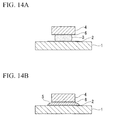
- a Au-Sn alloy solder paste 3 is mounted or applied on a metallization layer 2 formed on the surface of a substrate 1, and a chip 4 is mounted on the Au-Sn alloy solder paste 3 such that a metallization layer 6 of the chip 4 comes into contact with the Au-Sn alloy solder paste 3.
- a cooling process is performed, as shown in a longitudinal cross-sectional view of FIG.
- the substrate 1 and the chip 4 are bonded to each other with a Au-Sn alloy solder bonding layer 5 interposed therebetween (see Japanese Unexamined Patent Application, First Publication No. 2007-61857 ).
- the area of the metallization layer 2 formed on the surface of the substrate 1 is equal to or more than that of the metallization layer 6 of the chip 4.
- the chip 4 has a square shape. However, in some cases, the chip 4 has a rectangular shape.
- FIG. 15 is a plan view as viewed from the upper side of FIG. 14A .
- the Au-Sn alloy solder paste 3 is mounted or applied to the metallization layer 2 of the substrate 1.
- the chip 4 is mounted on the Au-Sn alloy solder paste 3 such that the center of the chip 4 and the center of the metallization layer 2 of the substrate 1 are arranged on the same axis and in the same direction.
- a Au-Sn alloy solder bonding layer 5 is formed on the entire surface of the metallization layer 2 of the substrate 1 by the Au-Sn alloy solder melted in the reflow process.
- the chip 4 temporarily floats on the molten Au-Sn alloy solder. In this case, the chip 4 is rotated or moved. After the cooling process, as shown in FIG. 16 , which is a plan view as viewed from the upper side of FIG. 14B , in many cases, the chip 4 is soldered to the Au-Sn alloy solder bonding layer 5 on the metallization layer 2 while being inclined with respect to the metallization layer 2 of the substrate 1 so as to deviate from the center of the metallization layer 2 of the substrate 1.
- a plurality of metallization layers is formed in a line on a wide substrate.
- a Au-Sn alloy solder paste is mounted or applied to the plurality of metallization layers and chips are regularly mounted on the Au-Sn alloy solder paste.
- the chips are put into a heating furnace and the chips are soldered to the substrate by one reflow process.
- the chips are rotated and soldered to the substrate while being inclined with respect to the arranged metallization layers of the substrate so as to deviate from the central of the metallization layer in a random direction, which is not preferable as a product to be shipped.
- the chips are likely to contact each other.
- the present invention uses the following methods.
- the inventors have conducted a study on a bonding method capable of soldering a chip to a substrate such that the chip is constantly disposed at the same position with respect to a metallization layer of the substrate and is aligned in a given direction. As a result, it was found that the position and direction of the chip after soldering was able to be aligned in the following embodiments.
- the thickness of the metallization layer 12 is not particularly limited, but it is preferable that the thickness of the metallization layer 12 be, for example, equal to or more than 0.02 ⁇ m and equal to or less than 50 ⁇ m. It is more preferable that the thickness of the metallization layer 12 be, for example, equal to or more than 0.05 ⁇ m and equal to or less than 10 ⁇ m.
- a material forming the outermost surface of the metallization layer 12 is not particularly limited, but it is preferable that the outermost surface of the metallization layer 12 be made of, for example, Au, Ag, or Cu in terms of the wettability of solder.
- the metallization layer is formed by, for example, a plating method, a sputtering method, or a coating method.
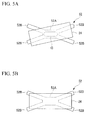
- the width W1 of the solder guide portion 12B is not particularly limited. However, for example, the width W1 of the solder guide portion 12B is preferably in the range of 5% to 50% of the length of one side of the main portion 12A, and more preferably in the range of 10% to 40% of the length. When the width W1 is too small or too large, the effect of positioning the chip 14 is reduced. As shown in FIG. 2B , the length L1 of the solder guide portion 12B may be set such that, when the solder guide portion 12B is arranged along the diagonal line of the chip 14 with the leading end of the solder guide portion 12B aligned with the corner of the chip 14, the entire metallization layer 12 including the rear end of the metallization layer 12 is exactly concealed by the chip 14.
- the length L1 of the solder guide portion 12B is preferably 20% to 70% of the length of one side of the metallization layer main portion 12A, and more preferably, 30% to 50% of the length within the range satisfying the above-mentioned conditions.
- AAu-Sn alloy solder paste 13 is mounted on the metallization layer main portion 12A.
- the amount of paste 13 may be equal to that in the conventional method.
- the thickness of the solder bonding layer after soldering is preferably in the range of 1 ⁇ m to 25 ⁇ m and more preferably in the range of 1 ⁇ m to 10 ⁇ m.
- the chip 14 with an area more than that of the metallization layer main portion 12A is mounted on the Au-Sn alloy solder paste 13 in an arbitrary direction. At that time, in the present invention, even though an accurate positioning process is not performed, it is possible to align the direction of the chip 14 after soldering using the solder guide portion 12B. Therefore, it is possible to reduce a production cost corresponding to a reduction in the positioning accuracy during assembly.
- the solder paste 13 is melted, and the chip 14 is rotated and moved to a relative position ( FIG. 2B ) where the overlap area between the metallization, layer 16 of the chip 14 and the metallization layer 12 of the substrate 10 is maximized by the surface tension of the molten solder.
- FIG. 2B the chip 14 is rotated such that the longest diagonal line (when the chip is square or rectangular, the longest diagonal line is a general diagonal line; and when the chip is elliptical, the longest diagonal line is the major axis) is aligned with the direction in which the solder guide portion 12B protrudes and is then soldered.
- the direction of the solder guide portion 12B is aligned in advance, and the chips having the same shape are soldered in a given direction.
- the chip 14 may be moved to a portion 14' represented by a two-dot chain line. It is considered that the chip 14 is soldered in a given direction because the molten solder flows from the metallization layer main portion 12A to the solder guide portion 12B and the chip 14 is rotated.
- the metallization layer main portion 12A and the solder guide portion 12B protruding from the metallization layer main portion 12A may be used as an electrode film of a semiconductor chip, such as an LED (light emitting diode) chip, a GaAs optical chip, a GaAs high-frequency chip, or a heat transfer chip.
- a semiconductor chip such as an LED (light emitting diode) chip, a GaAs optical chip, a GaAs high-frequency chip, or a heat transfer chip.
- the solder paste be a Au-Sn alloy solder paste.
- the following solder paste may be used: a Pb-Sn alloy solder paste obtained by mixing a flux with Pb-Sn alloy solder powder including 35 mass% to 60 mass% of Pb and the balance composed af Sn and inevitable impurities; a Pb-Sn alloy solder paste obtained by mixing a flux with Pb-Sn alloy solder powder including 90 mass% to 95 mass% af Pb and the balance composed of Sn and inevitable impurities; or a Pb-free solder paste obtained by mixing a flux with Pb-free alloy solder powder including 40 mass% to 100 mass% of Sn and the balance composed of one or more kinds of metal selected from a group including Ag, Au, Cu, Bi, Sb, In, and Zn and inevitable impurities.
- the same effect as that when the Au-Sn alloy solder paste is used is obtained.
- FIGS. 3A to 13 Other embodiments of the present invention are shown in FIGS. 3A to 13 .
- a metallization layer 22 may include a circular metallization layer main portion 22A and a rectangular solder guide portion 22B that protrudes from the outer circumference of the circular metallization layer main portion 22A in the radius direction.
- the metallization layer main portion may have any planar shape other than a circular shape.
- the solder guide portion may protrude from any position of the periphery of the metallization layer main portion.
- a metallization layer 32 including a square metallization layer main portion 32A and a solder guide portion 32B that protrudes from one vertex of the metallization layer main portion 32A in the extension direction of a diagonal line may be formed.
- FIG. 4A is a plan view illustrating still another embodiment.
- a metallization layer 42 formed on the surface of the substrate 10 includes a square metallization layer main portion 42A and four solder guide portions 42B that vertically protrude from the centers of four sides of the metallization layer main portion 42A.
- the angle formed between adjacent solder guide portions 42B is 90° and equal to the angle between the diagonal lines of the chip 14 to be bonded.
- the Au-Sn alloy solder paste 13 is mounted on the metallization layer main portion 42A, and the square chip 14 with an area more than that of the metallization layer main portion 42A is mounted on the Au-Sn alloy solder paste 13 in an arbitrary direction.
- the chip 14 is rotated such that the diagonal line of the square chip 14 is aligned with the longitudinal direction of the solder guide portion 42B by the surface tension of the molten solder and is then soldered, as shown in the plan view of FIG. 4B .
- all of the square chips on the substrate 10 are soldered while being aligned in a given direction.
- the other conditions are the same as those of the first embodiment.
- a metallization layer 52 including a metallization layer main portion 52A and four solder guide portions 52B that protrude from the metallization layer main portion 52A so as to intersect the diagonal lines of the rectangular chip 24 at the same angle is formed on the surface of the substrate.
- the Au-Sn alloy solder paste 13 is mounted on the metallization layer main portion 52A.
- the rectangular chip 24 is mounted on the Au-Sn alloy solder paste 13 in an arbitrary direction.
- the diagonal direction of the rectangular chip 24 is aligned with the direction of the solder guide portion 52B. As a result, it is possible to solder the rectangular chip 24 in a given direction.
- the other conditions are the same as those of the first embodiment.
- the phenomenon shown in (v) is not limited to the substrate and the square chip, but also occurs when a general square part is mounted on the substrate.
- the phenomenon shown in (vi) is not limited to the substrate and the rectangular chip, but also occurs when a general rectangular part is bonded to the substrate. Therefore, it is possible to apply this phenomenon to the bonding between the substrate and a square part or the bonding between the substrate and a rectangular part, thereby soldering the part to the substrate at a given position and in a given direction.
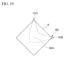
- FIGS. 6 to 10 show metallization layers each having a metallization layer main portion and a plurality of solder guide portions that protrude from the periphery of the metallization layer main portion so as to intersect the diagonal lines of a square part (chip) 14 at the same angle.
- the Au-Sn alloy solder paste is mounted on the metallization layer main portion.
- the square part (chip) 14 with an area more than that of the metallization layer main portion is mounted on the Au-Sn alloy solder paste in an arbitrary direction.
- FIGS. 6 to 10 show the soldered square part (chip) 14 after the reflow process is performed in this state.
- the size of a metallization layer main portion 62A may be equal to the width of a solder guide portion 62B of a metallization layer 62.
- the metallization layer main portion 62A may have an area capable of mounting or applying a solder paste.
- the solder guide portion may have a strip shape with a constant width, as shown in FIG. 4B , but the shape of the solder guide portion is not limited thereto.
- the solder guide portion may be triangular.
- a metallization layer 72 including a square metallization layer main portion 72A and triangular solder guide portions 72B that protrude from four sides of the metallization layer main portion 72A may be provided.
- a metallization layer 102 including a square metallization layer main portion 102A and two triangular solder guide portions 102B that protrude from two adjacent sides of the metallization layer main portion 102A may be provided.
- the number of solder guide portions be four, as shown in FIGS. 4B , 6, and 7 .
- the number of solder guide portions may be two.
- the number of solder guide portions may be three or five or more.
- a metallization layer 82 including a square metallization layer main portion 82A and two solder guide portions 82B that vertically protrude from two adjacent sides of the metallization layer main portion 82A may be provided.
- a metallization layer 92 including a square metallization layer main portion 92A and two solder guide portions 92B with a width equal to that of one side of the metallization layer main portion 92A may be provided.
- FIG. 11 shows a metallization layer including a rectangular metallization layer main portion 112A and two solder guide portions 112B that protrude from both ends of one short side of the metallization layer main portion 112A.
- the angle between the two solder guide portions 112B is equal to the intersection angle between two diagonal lines of a rectangular part (chip).
- the Au-Sn alloy solder paste is mounted on the metallization layer main portion 112A.
- a rectangular part (chip) 34 with an area more than that of the metallization layer main portion is mounted on the Au-Sn alloy solder paste in an arbitrary direction.
- FIG. 11 shows the soldered rectangular part (chip) 34 after the reflow process is performed in this state.
- FIG. 12 shows a metallization layer including a rectangular metallization layer main portion 122A and three solder guide portions 122B that protrude from three corners of the metallization layer main portion 122A.
- the angle between the three solder guide portions 122B is equal to the intersection angle between two diagonal lines of the rectangular part (chip) at the corresponding positions.
- the Au-Sn alloy solder paste is mounted on the metallization layer main portion 122A.
- the rectangular part (chip) 34 is mounted on the Au-Sn alloy solder paste in an arbitrary direction, and the reflow process is performed. As a result, the soldering state shown in FIG. 12 is obtained.
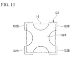
- the metallization layer may have a shape in which a semicircular portion is cut out from the center of each side of the square metallization layer.
- the metallization layer 132 includes a metallization layer main portion 132A and four solder guide portions 132B that extend from the periphery of the metallization layer main portion 132A in four directions.
- Au-Sn alloy solder powder having a composition including 20 mass% of Sn and the balance composed of Au and having an average particle diameter D 50 of 11.1 ⁇ m and a maximum particle diameter of 20.1 ⁇ m was used as a solder alloy.
- a commercial RMA flux was mixed with the Au-Sn alloy solder powder such that a composition including 8.0 mass% of RMA flux and the balance composed of Au-Sn alloy solder powder was obtained, thereby producing a Au-Sn alloy solder paste with a paste viscosity of 85 Pa ⁇ s.
- the Au-Sn alloy solder paste was filled in a syringe and the syringe was mounted in a dispenser (model number: ML-606GX manufactured by Musashi Engineering, Inc.).
- LED chips each having a dimension of a length of 400 ⁇ m, a width of 400 ⁇ m, and a height of 100 ⁇ m were prepared; and a Au film having a dimension of a thickness of 3 ⁇ m, a length of 400 ⁇ m, and a width of 400 ⁇ m was formed on the entire one surface of each of the LED chips by plating.
- Each of the metallization layers included a metallization layer main portion, which was a composite metallization layer including a Cu layer having a dimension of a length of 200 ⁇ m, a width of 200 ⁇ m, and a thickness of 10 ⁇ m; a Ni layer having a dimension of a length of 200 ⁇ m, a width of 200 ⁇ m, and a thickness of 5 ⁇ m; and a Au layer having a dimension of a length of 200 ⁇ m, a width of 200 ⁇ m, and a thickness of 0.1 ⁇ m; and a solder guide portion having a dimension of a width of 100 ⁇ m and a length of 90 ⁇ m, which was a composite metallization layer having the same structure as that of the metallization layer main portion.
- the solder guide portion protruded
- the deviation of the central positions of the bonded 50 LED chips, which were arranged in a line in the x-axis direction, in the y-axis direction was calculated as the standard deviation of the average y-axis position.
- the deviation of the chip central position in the y-axis direction was ⁇ 4.2 ⁇ m, and the position accuracy of the chip was very high.
- Pb-Sn alloy solder powder having a composition including 37 mass% of Pb and the balance composed of Sn and having an average particle diameter D 50 of 11.4 ⁇ m and a maximum particle diameter of J.4.5 ⁇ m was used as a solder alloy.
- a commercial RMA flux was mixed with the Pb-Sn alloy solder powder such that a composition including 11.0 mass% of RMA flux and the balance composed of Pb-Sn alloy solder powder was obtained, thereby producing a Pb-Sn alloy solder paste with a paste viscosity of 120 Pa.s.
- the Pb-Sn alloy solder paste was filled in a syringe and the syringe was mounted in a dispenser (model number: ML-606GX manufactured by Musashi Engineering, Inc.).
- the dispenser was used to apply 0.02 mg of Pb-Sn alloy solder paste onto 50 metallization layers each having the metallization layer main portion and the solder guide portion manufactured in Example 1.
- the previously prepared 50 LED chips were mounted on the Pb-Sn alloy solder paste.
- a reflow process of maintaining the chips under the conditions of a nitrogen atmosphere, and a temperature of 220°C was performed for 30 seconds.
- a cooling process was performed and the central positions of the 50 LED chips were measured by a three-dimensional measuring machine (NEXIV VMR-3020 manufactured by Nikon).
- the deviation of the central positions of the bonded 50 LED chips, which were arranged in a line in the x-axis direction, in the y-axis direction was calculated as the standard deviation of the average y-axis position.
- the deviation of the chip central position in the y-axis direction was +5.8 ⁇ m, and the position accuracy of the chip was very high.
- Pb-Sn alloy solder powder having a composition including 95 mass% of Pb and the balance composed of Sn and having an average particle diameter D 50 of 11.7 ⁇ m and a maximum particle diameter of 14.8 ⁇ m was used as a solder alloy.
- a commercial RA flux was mixed with the Pb-Sn alloy solder powder such that a composition including 10.0 mass% of RA flux and the balance composed of Pb-Sn alloy solder powder was obtained, thereby producing a Pb-Sn alloy solder paste with a paste viscosity of 80 Pa.s.
- the Pb-Sn alloy solder paste was filled in a syringe and the syringe was mounted in a dispenser (model number: ML-606GX manufactured by Musashi Engineering, Inc.).
- the dispenser was used to apply 0.03 mg of Pb-Sn alloy solder paste onto 50 metallization layers each having the metallization layer main portion and the solder guide portion manufactured in Example 1.
- the previously prepared 50 LED chips were mounted on the Pb-Sn alloy solder paste, and a reflow process of maintaining the chips under the conditions of a nitrogen atmosphere, and a temperature of 330°C was performed for 30 seconds. Then, a cooling process was performed and the central positions of the 50 LED chips were measured by a three-dimensional measuring machine (NEXIV VMR-3020 manufactured by Nikon).
- the deviation of the central positions of the bonded 50 LED chips, which were arranged in a line in the x-axis direction, in the y-axis direction was calculated as the standard deviation of the average y-axis position.
- the deviation of the chip central position in the y-axis direction was ⁇ 6.7 ⁇ m, and the position accuracy of the chip was very high.
- Pb-free solder powder having a composition including 96.5 mass% of Sn, 3.0 mass% of Ag, and the balance composed of Cu and having an average particle diameter D 50 of 10.8 ⁇ m and a maximum particle diameter of 14.1 ⁇ m was used as a solder alloy.
- a commercial RMA flux was mixed with the Pb-free solder powder such that a composition including 12.5 mass% of RMA flux and the balance composed of Pb-free solder powder was obtained, thereby producing a Pb-free solder paste with a paste viscosity of 72 Pa ⁇ s.
- the Pb-free solder paste was filled in a syringe and the syringe was mounted in a dispenser (model number: ML-606GX manufactured by Musashi Engineering, Inc.).
- the dispenser was used to apply 0.02 mg of Pb-free solder paste onto 50 metallization layers each having the metallization layer main portion and the solder guide portion manufactured in Example 1.
- the previously prepared 50 LED chips were mounted on the Pb-free solder paste, and a reflow process of maintaining the chips under the conditions of a nitrogen atmosphere, and a temperature of 240°C was performed for 30 seconds.
- a cooling process was performed and the central positions of the 50 LED chips were measured by a three-dimensional measuring machine (NEXIV VMR-3020 manufactured by Nikon).
- the deviation of the central positions of the bonded 50 LED chips, which were arranged in a line in the x-axis direction, in the y-axis direction was calculated as the standard deviation of the average y-axis position.
- the deviation of the chip central position in the y-axis direction was ⁇ 5.1 ⁇ m, and the position accuracy of the chip was very high.
- Au-Sn alloy solder powder having a composition including 20 mass% of Sn and the balance composed of Au and having an average particle diameter D 50 of 11.1 ⁇ m and a maximum particle diameter of 20.1 ⁇ m was used as a solder alloy.
- a commercial RMA flux was mixed with the Au-Sn alloy solder powder such that a composition including 8.0 mass% of RMA flux and the balance of Au-Sn alloy solder powder was obtained, thereby producing a Au-Sn alloy solder paste with a paste viscosity of 85 Pa ⁇ s.
- the Au-Sn alloy solder paste was filled in a syringe and the syringe was mounted in a dispenser (model number: ML-606GX manufactured by Musashi Engineering, Inc.).
- LED chips each having a dimension of a length of 400 ⁇ m, a width of 400 ⁇ m, and a height of 100 ⁇ m were prepared; and aAu film having a dimension of a thickness of 3 ⁇ m, a length of 400 ⁇ m, and a width of 400 ⁇ m was formed on entire one surface of each of the LED chips by plating.
- An alumina substrate was prepared, and 50 metallization layers shown in FIG. 15 , which were composite metallization layers each including a Cu layer having a dimension of a length of 500 ⁇ m, a width of 500 ⁇ m, and a thickness of 10 ⁇ m; a Ni layer having a dimension of a length of 500 ⁇ m, a width of 500 ⁇ m, and a thickness of 5 ⁇ m; and a Au layer having a dimension of a length of 500 ⁇ m, a width of 500 ⁇ m, and a thickness of 0.1 ⁇ m; were formed in a line on the surface of the alumina substrate at an interval of 600 ⁇ m.
- the deviation of the central positions of the bonded 50 LED chips, which were arranged in a line in the x-axis direction, in the y-axis direction was calculated as the standard deviation of the average y-axis position.
- the deviation of the chip central position in the y-axis direction was +38.2 ⁇ m, and the position accuracy of the chip was low.
- Au-Sn alloy solder powder having a composition including 20 mass% of Sn and the balance composed of Au and having an average particle diameter D 50 of 11.1 ⁇ m and a maximum particle diameter of 20.1 ⁇ m was used as a solder alloy.
- a commercial RMA flux was mixed with the Au-Sn alloy solder powder such that a composition including 8.0 mass% of RMA flux and the balance composed of Au-Sn alloy solder powder was obtained, thereby producing a Au-Sn alloy solder paste with a paste viscosity of 85 Pa ⁇ s.
- the Au-Sn alloy solder paste was filled in a syringe and the syringe was mounted in a dispenser (model number: ML-606GX manufactured by Musashi Engineering, Inc.).
- 50 square LED chips each having a dimension of a length of 400 ⁇ m, a width of 400 ⁇ m, and a height of 100 ⁇ m were prepared; and a Au film having a dimension of a thickness of 3 ⁇ m, a length of 400 ⁇ m, and a width of 400 ⁇ m was formed on the entire one surface of each of the LED chips by plating.
- An alumina substrate was prepared, and 50 metallization layers having a planar shape shown in FIG. 4B were formed in a line on the surface of the alumina substrate at an interval of 600 ⁇ m.
- Each of the metallization layers included a metallization layer main portion, which was a composite metallization layer including a Cu layer having a dimension of a length of 200 ⁇ m, a width of 200 ⁇ m, and a thickness of 10 ⁇ m; a Ni layer having a dimension of a length of 200 ⁇ m, a width of 200 ⁇ m, and a thickness of 5 ⁇ m; and a Au layer having a dimension of a length of 200 ⁇ m, a width of 200 ⁇ m, and a thickness of 0.1 ⁇ m; and a solder guide portion that protruded from the metallization layer main portion in a cross shape and had a dimension of a width of 50 ⁇ m and a length of 150 ⁇ m, which was a composite metallization layer having the same structure as the metallization layer main portion.
- the deviations of the central positions of the bonded 50 LED chips in the y-axis direction and the x-axis direction were calculated as the standard deviation of the average y-axis position and the standard deviation of the average x-axis position, respectively.
- the deviation of the chip central position in the x-axis direction was ⁇ 4.8 ⁇ m
- the deviation of the chip central position in the y-axis direction was ⁇ 5.2 ⁇ m. Accordingly, the position accuracy of the chip was very high.
- Pb-Sn alloy solder powder having a composition including 37 mass% of Pb and the balance composed of Sn and having an average particle diameter D 50 of 11.4 ⁇ m and a maximum particle diameter of 14.5 ⁇ m was used as a solder alloy.
- a commercial RMA flux was mixed with the Pb-Sn alloy solder powder such that a composition including 11.0 mass% of RMA flux and the balance composed of Pb-Sn alloy solder powder was obtained, thereby producing a Pb-Sn alloy solder paste with a paste viscosity of 120 Pa.s.
- the Pb-Sn alloy solder paste was filled in a syringe and the syringe was mounted in a dispenser (model number: ML-606GX manufactured by Musashi Engineering, Inc.).
- Each of the metallization layers included a metallization layer main portion, which was a composite metallization layer including a Cu layer having a dimension of a length of 100 ⁇ m, a width of 200 ⁇ m, and a thickness of 10 ⁇ m; a Ni layer having a dimension of a length of 100 ⁇ m, a width of 200 ⁇ m, and a thickness of 5 ⁇ m; and a Au layer having a dimension of a length of 100 ⁇ m, a width of 200 ⁇ m, and a thickness of 0.1 ⁇ m; and four solder guide portions that protruded from the metallization layer main portion at the same angle as the diagonal line of the rectangular LED chip and had a dimension of a width of 50 ⁇ m and a length of 150 ⁇ m, which were a composite metallization layer
- the deviations of the central positions of the bonded 50 LED chips in the x-axis direction and the y-axis direction were calculated as the standard deviation of the average x-axis position and the standard deviation of the average y-axis position, respectively.
- the deviation of the chip central position in the x-axis direction was ⁇ 7.1 ⁇ m
- the deviation of the chip central position in the y-axis direction was ⁇ 6.8 ⁇ m. Accordingly, the position accuracy of the chip was very high.
- Pb-Sn alloy solder powder having a composition including 95 mass% of Pb and the balance composed of Sn and having an average particle diameter D 50 of 11.7 ⁇ m and a maximum particle diameter of 14.8 ⁇ m was used as a solder alloy.
- a commercial RA flux was mixed with the Pb-Sn alloy solder powder such that a composition including 10.0 mass% of RA flux and the balance composed of Pb-Sn alloy solder powder was obtained, thereby producing a Pb-Sn alloy solder paste with a paste viscosity of 80 Pa ⁇ s.
- the Pb-Sn alloy solder paste was filled in a syringe and the syringe was mounted in a dispenser (model number: ML-606GX manufactured by Musashi Engineering, Inc.).
- An alumina substrate was prepared, and 50 metallization layers having the planar shape shown in FIG. 11 were formed in a line on the surface of the alumina substrate at an interval of 600 ⁇ m.
- Each of the metallization layers included a metallization layer main portion, which was a composite metallization layer including a Cu layer having a dimension of a length of 100 ⁇ m, a width of 200 ⁇ m, and a thickness of 10 ⁇ m; a Ni layer having a dimension of a length of 100 ⁇ m, a width of 200 ⁇ m, and a thickness of 5 ⁇ m; and a Au layer having a dimension of a length of 100 ⁇ m, a width of 200 ⁇ m, and a thickness of 0.1 ⁇ m; and two solder guide portions that protruded from the metallization layer main portion at the same angle as the diagonal line of the rectangular LED chip and had a dimension of a width of 100 ⁇ m and a length of 150 ⁇ m, which were a composite metallization
- the deviations of the central positions of the bonded 50 LED chips in the x-axis direction and the y-axis direction were calculated as the standard deviation of the average x-axis position and the standard deviation of the average y-axis position, respectively.
- the deviation of the chip central position in the x-axis direction was ⁇ 6.6 ⁇ m
- the deviation of the chip central position in the y-axis direction was ⁇ 7.2 ⁇ m. Accordingly, the position accuracy of the chip was very high.
- Pb-free solder powder having a composition including 96.5 mass% of Sn, 3.0 mass% of Ag, and the balance composed of Cu and having an average particle diameter D 50 of 10.8 ⁇ m and a maximum particle diameter of 14.1 ⁇ m was used as a solder alloy.
- a commercial RMA flux was mixed with the Pb-free solder powder such that a composition including 12.5 mass% of RMA flux and the balance composed of Pb-free solder powder was obtained, thereby producing a Pb-free solder paste with a paste viscosity of 72 Pa ⁇ s.
- the Pb-free solder paste was filled in a syringe and the syringe was mounted in a dispenser (model number: ML-606GX manufactured by Musashi Engineering, Inc.).
- 50 square LED chips each having a dimension of a length of 400 ⁇ m, a width of 400 ⁇ m, and a height of 100 ⁇ m were prepared; and a Au film having a dimension of a thickness of 3 ⁇ m, a length of 400 ⁇ m, and a width of 400 ⁇ m was formed on the entire one surface of each of the LED chips by plating.
- An alumina substrate was prepared, and 50 metallization layers having the planar shape shown in FIG. 8 were formed in a line on the surface of the alumina substrate at an interval of 600 ⁇ m.
- Each of the metallization layers included a metallization layer main portion, which was a composite metallization layer including a Cu layer having a dimension of a length of 200 ⁇ m, a width of 200 ⁇ m, and a thickness of 10 ⁇ m; a Ni layer having a dimension of a length of 200 ⁇ m, a width of 200 ⁇ m, and a thickness of 5 ⁇ m; and a Au layer having a dimension of a length of 200 ⁇ m, a width of 200 ⁇ m, and a thickness of 0.1 ⁇ m; and two solder guide portions that protruded from the metallization layer main portion in an L shape and had a dimension of a width of 100 ⁇ m and a length of 200 ⁇ m, which were a composite metallization layer having the same structure as the metallization layer main portion.
- the deviations of the central positions of the bonded 50 LED chips in the x-axis direction and the y-axis direction were calculated as the standard deviation of the average x-axis position and the standard deviation of the average y-axis position, respectively.
- the deviation of the chip central position in the x-axis direction was ⁇ 9.3 ⁇ m
- the deviation of the chip central position in the y-axis direction was ⁇ 8.9 ⁇ m. Accordingly, the position accuracy of the chip was very high.
- Au-Sn alloy solder powder having a composition including 20 mass% of Sn and the balance composed of Au and having an average particle diameter D 50 of 11.1 ⁇ m and a maximum particle diameter of 20.1 ⁇ m was used as a solder alloy.
- a commercial RMA flux was mixed with the Au-Sn alloy solder powder such that a composition including 8.0 mass% of RMA flux and the balance composed of Au-Sn alloy solder powder was obtained, thereby producing aAu-Sn alloy solder paste with a paste viscosity of 85 Pa ⁇ s.
- the Au-Sn alloy solder paste was filled in a syringe and the syringe was mounted in a dispenser (model number: ML-606GX manufactured by Musashi Engineering, Inc.).
- LED chips each having a dimension of a length of 400 ⁇ m, a width of 400 ⁇ m, and a height of 100 ⁇ m were prepared; and a Au film having a dimension of a thickness of 3 ⁇ m, a length of 400 ⁇ m, and a width of 400 ⁇ m was formed on the entire one surface of each of the LED chips by plating.
- An alumina substrate was prepared, and 50 metallization layers, which were composite metallization layers each including a Cu layer having a dimension of a length of 500 ⁇ m, a width of 500 ⁇ m, and a thickness of 10 ⁇ m; a Ni layer having a dimension of a length of 500 ⁇ m, a width of 500 ⁇ m, and a thickness of 5 ⁇ m; and a Au layer having a dimension of a length of 500 ⁇ m, a width of 500 ⁇ m, and a thickness of 0.1 ⁇ m were formed in a line on the surface of the alumina substrate at an interval of 600 ⁇ m.
- 0.03 mg ofAu-Sn alloy solder paste was applied onto the center of each of the 50 metallization layers, which were the composite metallization layers, by a previously prepared dispenser.
- the previously prepared 50 LED chips were mounted on the Au-Sn alloy solder paste by a mounter. In this state, a reflow process of maintaining the chips under the conditions of a nitrogen atmosphere, and a temperature of 300°C was performed for 30 seconds. Then, a cooling process was performed and the central positions of the 50 LED chips arranged in a line were measured by a three-dimensional measuring machine (NEXIV VMR-3020 manufactured by Nikon).
- the deviations of the central positions of the bonded 50 LED chips, which were arranged in a line in the x-axis direction, in the x-axis direction and the y-axis direction was calculated as the standard deviation of the average x-axis position and the standard deviation of the average y-axis position, respectively.
- the deviation of the chip central position in the x-axis direction was ⁇ 42.1 ⁇ m
- the deviation of the chip central position in the y-axis direction was ⁇ 37.5 ⁇ m. Accordingly, the position accuracy of the chip was low.
- the present invention provides a method of bonding parts to a substrate using solder paste such that the parts are disposed at the same position and are aligned in the same direction, particularly, a method of bonding chips to a substrate using a Au-Sn alloy solder paste such that the chips are disposed at the same position and are aligned in the same direction. Therefore, the present invention has industrial applicability.
Landscapes
- Engineering & Computer Science (AREA)
- Mechanical Engineering (AREA)
- Chemical & Material Sciences (AREA)
- Materials Engineering (AREA)
- Metallurgy (AREA)
- Organic Chemistry (AREA)
- Microelectronics & Electronic Packaging (AREA)
- Manufacturing & Machinery (AREA)
- Electric Connection Of Electric Components To Printed Circuits (AREA)
Abstract
Description
- The present invention relates to a method of bonding parts to a substrate using a solder paste such that the parts are disposed at the same position and are aligned in the same direction, and more particularly, to a method of bonding chips to a substrate using a Au-Sn alloy solder paste such that the chips are disposed at the same position and are aligned in the same direction.
- Priority is claimed on Japanese Patent Application No.
2008-154003, filed June 12, 2008 2008-221633, filed August 29, 2008 - In general, for example, a Au-Sn alloy solder paste has been used to bond a substrate and a semiconductor chip, such as an LED (light emitting diode) chip, a GaAs optical chip, a GaAs high-frequency chip, or a heat transfer chip. AAu-Sn alloy solder paste has been known which is obtained by mixing Au-Sn eutectic alloy gas-atomized powder having a composition including 15 mass% to 25 mass% of Sn (preferably, 20 mass% of Sn) and the balance composed of Au and inevitable impurities with a commercial flux including rosin, an activator, a solvent, and a viscosity improver.
- When the Au-Sn alloy solder paste is used to bond the chip and the substrate, there are the following advantages. Since a Au-Sn alloy solder bonding layer is made of a Au-Sn solder alloy, the thermal conductivity and bonding reliability are high. Since the Au-Sn alloy solder paste is paste, it is possible to collectively supply the Au-Sn alloy solder paste to a plurality of bonding portions and collectively perform a heat treatment thereon. In addition, during a reflow process, since a flux covers the surface of the Au-Sn solder alloy, an oxide film is less likely to be formed. Therefore, the fluidity of a molten Au-Sn solder alloy is high during bonding and the wettability thereof is high. Therefore, it is possible to use the entire surface of the chip as a bonding surface. Further, it is not necessary to apply an excessive load to the chip during bonding.
- In order to bond the substrate and the chip using the Au-Sn alloy solder paste, first, as shown in a longitudinal cross-sectional view of
FIG. 14A , a Au-Snalloy solder paste 3 is mounted or applied on ametallization layer 2 formed on the surface of asubstrate 1, and achip 4 is mounted on the Au-Snalloy solder paste 3 such that ametallization layer 6 of thechip 4 comes into contact with the Au-Snalloy solder paste 3. In this state, when heat is applied to perform a reflow process and then a cooling process is performed, as shown in a longitudinal cross-sectional view ofFIG. 14B , thesubstrate 1 and thechip 4 are bonded to each other with a Au-Sn alloysolder bonding layer 5 interposed therebetween (see Japanese Unexamined Patent Application, First Publication No.2007-61857 metallization layer 2 formed on the surface of thesubstrate 1 is equal to or more than that of themetallization layer 6 of thechip 4. In addition, in general, thechip 4 has a square shape. However, in some cases, thechip 4 has a rectangular shape. - Japanese Unexamined Patent Application, First Publication No.
2007-61857 -
FIG. 15 is a plan view as viewed from the upper side ofFIG. 14A . As shown inFIGS. 15 and14A , the Au-Snalloy solder paste 3 is mounted or applied to themetallization layer 2 of thesubstrate 1. Thechip 4 is mounted on the Au-Snalloy solder paste 3 such that the center of thechip 4 and the center of themetallization layer 2 of thesubstrate 1 are arranged on the same axis and in the same direction. However, when heat is applied to perform a reflow process in this state, a Au-Sn alloysolder bonding layer 5 is formed on the entire surface of themetallization layer 2 of thesubstrate 1 by the Au-Sn alloy solder melted in the reflow process. At the same time, thechip 4 temporarily floats on the molten Au-Sn alloy solder. In this case, thechip 4 is rotated or moved. After the cooling process, as shown inFIG. 16 , which is a plan view as viewed from the upper side ofFIG. 14B , in many cases, thechip 4 is soldered to the Au-Sn alloysolder bonding layer 5 on themetallization layer 2 while being inclined with respect to themetallization layer 2 of thesubstrate 1 so as to deviate from the center of themetallization layer 2 of thesubstrate 1. - In particular, in order to industrially solder the
chip 4 to the substrate, a plurality of metallization layers is formed in a line on a wide substrate. A Au-Sn alloy solder paste is mounted or applied to the plurality of metallization layers and chips are regularly mounted on the Au-Sn alloy solder paste. In this state, the chips are put into a heating furnace and the chips are soldered to the substrate by one reflow process. During the reflow process, the chips are rotated and soldered to the substrate while being inclined with respect to the arranged metallization layers of the substrate so as to deviate from the central of the metallization layer in a random direction, which is not preferable as a product to be shipped. In addition, when a package size is further reduced in the future and the distance between the chips is short, the chips are likely to contact each other. - In order to solve the above-mentioned problems and achieve an object of the present invention, the present invention uses the following methods.
- (1) According a method of bonding a part to a substrate using a solder paste in a first aspect of the present invention, the method includes mounting or applying the solder paste between a metallization layer formed on the substrate and a metallization layer formed on the part, and soldering the part and the substrate by performing a reflow process in a non-oxidizing atmosphere, wherein the metallization layer formed on the surface of the substrate is planar and includes a metallization layer main portion that has an area smaller than that of the metallization layer of the part and a solder guide portion that protrudes from a periphery of the metallization layer main portion.
- (2) The solder paste may be a Au-Sn alloy solder paste obtained by mixing a flux with a Au-Sn alloy solder powder including 20 mass% to 25 mass% of Sn and the balance composed of Au and inevitable impurities.
- (3) The solder paste may be a Pb-Sn alloy solder paste obtained by mixing a flux with a Pb-Sn alloy solder powder including 35 mass% to 60 mass% of Pb and the balance composed of Sn and inevitable impurities.
- (4) The solder paste may be a Pb-Sn alloy solder paste obtained by mixing a flux with a Pb-Sn alloy solder powder including 90 mass% to 95 mass% of Pb and the balance composed of Sn and inevitable impurities.
- (5) Te solder paste may be a Pb-free solder paste obtained by mixing a flux with a Pb-free alloy solder powder including 40 mass% to 100 mass% of Sn and the balance composed of one or more kinds of metal selected from a group consisting of Ag, Au, Cu, Bi, Sb, In, and Zn and inevitable impurities.
- (6) The part may be a chip.
- (7) The metallization layer formed on the substrate may be an electrode film.
- (8) According to a method of bonding a part to a substrate using a solder paste in a second aspect of the present invention, the method includes mounting or applying the solder paste between a metallization layer formed on the substrate and a metallization layer formed on the rectangular part, and soldering the part and the substrate by performing a reflow process in a non-oxidizing atmosphere. The metallization layer formed on the surface of the substrate is planar and includes a metallization layer main portion that has an area smaller than that of the metallization layer of the part, and at least two solder guide portions that protrude from the periphery of the metallization layer main portion, and the angle between two adjacent solder guide portions in the longitudinal direction is equal to an intersection angle between the diagonal lines of the part.
- (9) The rectangular part may include a square part.
- (10) According to a metallization layer formed on a surface of a substrate in a third aspect of the present invention, the metallization layer is planar and includes a metallization layer main portion and a solder guide portion protruding from the periphery of the metallization layer main portion.
- (11) In the metallization layer according to (10), the metallization layer formed on the substrate may be an electrode film.
- (12) According to a substrate having a metallization layer formed thereon in a fourth aspect of the present invention, the metallization layer is planar and includes a metallization layer main portion and a solder guide portion protruding from the periphery of the metallization layer main portion.
- (13) In the substrate according to (12), the metallization layer may be an electrode film.
- (14) According to a solder paste in a fifth aspect of the present invention, the solder paste may be a mixture of an alloy solder powder including at least Sn and a flux.
- (15) According to a bonded body of a part and a substrate in a sixth aspect of the present invention, the part and the substrate are bonded by the method of bonding according to any one of (1) to (9).
- (16) According to a method of producing a bonded body of a part and a substrate in a seventh aspect of the present invention, the bonded body of the part and the substrate is produced using the method of bonding according to any one of (1) to (9).
- According to a method of bonding a substrate and a part in the present invention, it is possible to solder all parts at desired positions and in a desired direction.
-
-
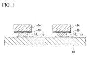
FIG. 1 is a longitudinal cross-sectional view illustrating the image of the overall structure before a reflow process in a method of bonding a substrate and a chip according to the present invention. -
FIG. 2A is a plan view illustrating the structure before the reflow process in the method according to the present invention. -
FIG. 2B is a plan view illustrating the structure after the reflow process in the method according to the present invention. -
FIG. 3A is a plan view illustrating the shape of a metallization layer formed on the substrate in the present invention. -
FIG. 3B is a plan view illustrating the shape of the metallization layer formed on the substrate in the present invention. -
FIG. 4A is a plan view illustrating the structure before the reflow process in the method according to the present invention. -
FIG. 4B is a plan view illustrating the structure after the reflow process in the method according to the present invention. -
FIG. 5A is a plan view illustrating the structure before the reflow process in the method according to the present invention. -
FIG. 5B is a plan view illustrating the structure after the reflow process in the method according to the present invention. -
FIG. 6 is a plan view illustrating the bonding between a metallization layer and a part according to another embodiment of the present invention. -
FIG. 7 is a plan view illustrating the bonding between a metallization layer and a part according to another embodiment of the present invention. -
FIG. 8 is a plan view illustrating the bonding between a metallization layer and a part according to another embodiment of the present invention. -
FIG. 9 is a plan view illustrating the bonding between a metallization layer and a part according to another embodiment of the present invention. -
FIG. 10 is a plan view illustrating the bonding between a metallization layer and a part according to another embodiment of the present invention. -
FIG. 11 is a plan view illustrating the bonding between a metallization layer and a part according to another embodiment of the present invention. -
FIG. 12 is a plan view illustrating the bonding between a metallization layer and a part according to another embodiment of the present invention. -
FIG. 13 is a plan view illustrating the bonding between a metallization layer and a part according to another embodiment of the present invention. -
FIG. 14A is a longitudinal cross-sectional view illustrating a structure before a reflow process in the conventional method. -
FIG. 14B is a longitudinal cross-sectional view illustrating the structure after the reflow process in the conventional method. -
FIG. 15 is a plan view illustrating a substrate and a chip in the state shown inFIG. 14A , as viewed from the upper side. -
FIG. 16 is a plan view illustrating the substrate and the chip in the state shown inFIG. 14B , as viewed from the upper side. - The inventors have conducted a study on a bonding method capable of soldering a chip to a substrate such that the chip is constantly disposed at the same position with respect to a metallization layer of the substrate and is aligned in a given direction. As a result, it was found that the position and direction of the chip after soldering was able to be aligned in the following embodiments.
-
- (i) As shown in a longitudinal cross-sectional view of
FIG. 1 , asubstrate 10 and achip 14 are bonded to each other through ametallization layer 12 of thesubstrate 10 and ametallization layer 16 of thechip 14 using asolder paste 13. The size of thechip 14 is not particularly limited in the present invention. However, for example, thechip 14 has one side with a length of equal to or more than 50 µm and equal to or less than 1 cm and a height of equal to or more than 10 µm and equal to or less than 5000 µm. For example, as a product, thechip 14 has one side with a length of equal to or more than 950 µm and equal to or less than 1100 µm and a height of equal to or more than 90 µm and equal to or less than 110 µm. In general, in a semiconductor chip, such as an LED (light emitting diode) chip, a GaAs optical chip, a GaAs high-frequency chip, or a heat transfer chip, a plurality of metallization layers 12 are formed on thesubstrate 10 at a predetermined interval. However, in the present invention, the plurality of metallization layers 12 may not be formed on thesubstrate 10 at a predetermined interval or onemetallization layer 12 may be formed. In this embodiment, as shown in a plan view ofFIG. 2A , themetallization layer 12 formed on the surface of thesubstrate 10 includes a metallization layermain portion 12A with a rectangular shape (a rectangular shape or a square shape) and asolder guide portion 12B that protrudes from the periphery of the metallization layermain portion 12A. In the embodiment, in particular, the thin rectangularsolder guide portion 12B vertically protrudes from the center of one side of themain portion 12A. In the embodiment, thesolder guide portion 12B has a constant width. However, thesolder guide portion 12B may have a trapezoidal shape or a triangular shape in which it is tapered toward its leading end. It is preferable that the area of the metallization layermain portion 12A be 30% to 95% of the area of thechip 14. - The thickness of the
metallization layer 12 is not particularly limited, but it is preferable that the thickness of themetallization layer 12 be, for example, equal to or more than 0.02 µm and equal to or less than 50 µm. It is more preferable that the thickness of themetallization layer 12 be, for example, equal to or more than 0.05 µm and equal to or less than 10 µm. A material forming the outermost surface of themetallization layer 12 is not particularly limited, but it is preferable that the outermost surface of themetallization layer 12 be made of, for example, Au, Ag, or Cu in terms of the wettability of solder. The metallization layer is formed by, for example, a plating method, a sputtering method, or a coating method. The width W1 of thesolder guide portion 12B is not particularly limited. However, for example, the width W1 of thesolder guide portion 12B is preferably in the range of 5% to 50% of the length of one side of themain portion 12A, and more preferably in the range of 10% to 40% of the length. When the width W1 is too small or too large, the effect of positioning thechip 14 is reduced. As shown inFIG. 2B , the length L1 of thesolder guide portion 12B may be set such that, when thesolder guide portion 12B is arranged along the diagonal line of thechip 14 with the leading end of thesolder guide portion 12B aligned with the corner of thechip 14, theentire metallization layer 12 including the rear end of themetallization layer 12 is exactly concealed by thechip 14. That is, it is preferable that two corners of the rear end of themetallization layer 12 be disposed immediately below or in the vicinity of a side of thechip 14. For example, the length L1 of thesolder guide portion 12B is preferably 20% to 70% of the length of one side of the metallization layermain portion 12A, and more preferably, 30% to 50% of the length within the range satisfying the above-mentioned conditions. - AAu-Sn
alloy solder paste 13 is mounted on the metallization layermain portion 12A. The amount ofpaste 13 may be equal to that in the conventional method. Specifically, the thickness of the solder bonding layer after soldering is preferably in the range of 1 µm to 25 µm and more preferably in the range of 1 µm to 10 µm. Thechip 14 with an area more than that of the metallization layermain portion 12A is mounted on the Au-Snalloy solder paste 13 in an arbitrary direction. At that time, in the present invention, even though an accurate positioning process is not performed, it is possible to align the direction of thechip 14 after soldering using thesolder guide portion 12B. Therefore, it is possible to reduce a production cost corresponding to a reduction in the positioning accuracy during assembly. - In this state, when a reflow process is performed in an inert gas atmosphere, the
solder paste 13 is melted, and thechip 14 is rotated and moved to a relative position (FIG. 2B ) where the overlap area between the metallization,layer 16 of thechip 14 and themetallization layer 12 of thesubstrate 10 is maximized by the surface tension of the molten solder. As shown inFIG. 2B , during the reflow process, thechip 14 is rotated such that the longest diagonal line (when the chip is square or rectangular, the longest diagonal line is a general diagonal line; and when the chip is elliptical, the longest diagonal line is the major axis) is aligned with the direction in which thesolder guide portion 12B protrudes and is then soldered. Therefore, the direction of thesolder guide portion 12B is aligned in advance, and the chips having the same shape are soldered in a given direction. In this case, thechip 14 may be moved to a portion 14' represented by a two-dot chain line. It is considered that thechip 14 is soldered in a given direction because the molten solder flows from the metallization layermain portion 12A to thesolder guide portion 12B and thechip 14 is rotated. - (ii) The metallization layer
main portion 12A and thesolder guide portion 12B protruding from the metallization layermain portion 12A may be used as an electrode film of a semiconductor chip, such as an LED (light emitting diode) chip, a GaAs optical chip, a GaAs high-frequency chip, or a heat transfer chip. - (iii) The phenomenon shown in (i) is not limited to the substrate and the chip, but also occurs in a general part mounted on the substrate. Therefore, the present invention may be applied to a general part.
- (iv) It is preferable that the solder paste be a Au-Sn alloy solder paste. However, instead of the Au-Sn alloy solder paste, the following solder paste may be used: a Pb-Sn alloy solder paste obtained by mixing a flux with Pb-Sn alloy solder powder including 35 mass% to 60 mass% of Pb and the balance composed af Sn and inevitable impurities; a Pb-Sn alloy solder paste obtained by mixing a flux with Pb-Sn alloy solder powder including 90 mass% to 95 mass% af Pb and the balance composed of Sn and inevitable impurities; or a Pb-free solder paste obtained by mixing a flux with Pb-free alloy solder powder including 40 mass% to 100 mass% of Sn and the balance composed of one or more kinds of metal selected from a group including Ag, Au, Cu, Bi, Sb, In, and Zn and inevitable impurities. In this case, the same effect as that when the Au-Sn alloy solder paste is used is obtained.
- Other embodiments of the present invention are shown in
FIGS. 3A to 13 . - It is preferable that the shape of the metallization layer main portion formed on the substrate be the same as that of the chip, but the shape of the metallization layer main portion is not particularly limited. For example, as shown in
FIG. 3A , ametallization layer 22 may include a circular metallization layermain portion 22A and a rectangularsolder guide portion 22B that protrudes from the outer circumference of the circular metallization layermain portion 22A in the radius direction. The metallization layer main portion may have any planar shape other than a circular shape. - The solder guide portion may protrude from any position of the periphery of the metallization layer main portion. For example, as shown in
FIG. 3B , ametallization layer 32 including a square metallization layermain portion 32A and asolder guide portion 32B that protrudes from one vertex of the metallization layermain portion 32A in the extension direction of a diagonal line may be formed. - (v)
FIG. 4A is a plan view illustrating still another embodiment. As shown inFIG. 4A , in this embodiment, ametallization layer 42 formed on the surface of thesubstrate 10 includes a square metallization layermain portion 42A and foursolder guide portions 42B that vertically protrude from the centers of four sides of the metallization layermain portion 42A. The angle formed between adjacentsolder guide portions 42B is 90° and equal to the angle between the diagonal lines of thechip 14 to be bonded. The Au-Snalloy solder paste 13 is mounted on the metallization layermain portion 42A, and thesquare chip 14 with an area more than that of the metallization layermain portion 42A is mounted on the Au-Snalloy solder paste 13 in an arbitrary direction. When the reflow process is performed in this state, thechip 14 is rotated such that the diagonal line of thesquare chip 14 is aligned with the longitudinal direction of thesolder guide portion 42B by the surface tension of the molten solder and is then soldered, as shown in the plan view ofFIG. 4B . As a result, all of the square chips on thesubstrate 10 are soldered while being aligned in a given direction. The other conditions are the same as those of the first embodiment. - (vi) When a
chip 24 with a rectangular shape is used, as shown inFIG. 5A , ametallization layer 52 including a metallization layermain portion 52A and foursolder guide portions 52B that protrude from the metallization layermain portion 52A so as to intersect the diagonal lines of therectangular chip 24 at the same angle is formed on the surface of the substrate. The Au-Snalloy solder paste 13 is mounted on the metallization layermain portion 52A. Therectangular chip 24 is mounted on the Au-Snalloy solder paste 13 in an arbitrary direction. When the reflow process is performed in this state, as shown inFIG. 5B , the diagonal direction of therectangular chip 24 is aligned with the direction of thesolder guide portion 52B. As a result, it is possible to solder therectangular chip 24 in a given direction. The other conditions are the same as those of the first embodiment. - (vii) The phenomenon shown in (v) is not limited to the substrate and the square chip, but also occurs when a general square part is mounted on the substrate. In addition, the phenomenon shown in (vi) is not limited to the substrate and the rectangular chip, but also occurs when a general rectangular part is bonded to the substrate. Therefore, it is possible to apply this phenomenon to the bonding between the substrate and a square part or the bonding between the substrate and a rectangular part, thereby soldering the part to the substrate at a given position and in a given direction.
-
FIGS. 6 to 10 show metallization layers each having a metallization layer main portion and a plurality of solder guide portions that protrude from the periphery of the metallization layer main portion so as to intersect the diagonal lines of a square part (chip) 14 at the same angle. In order to connect the chip and the substrate, the Au-Sn alloy solder paste is mounted on the metallization layer main portion. The square part (chip) 14 with an area more than that of the metallization layer main portion is mounted on the Au-Sn alloy solder paste in an arbitrary direction.FIGS. 6 to 10 show the soldered square part (chip) 14 after the reflow process is performed in this state. - As shown in the embodiment of
FIG. 6 , the size of a metallization layermain portion 62A may be equal to the width of asolder guide portion 62B of ametallization layer 62. The metallization layermain portion 62A may have an area capable of mounting or applying a solder paste. - It is preferable that the solder guide portion have a strip shape with a constant width, as shown in
FIG. 4B , but the shape of the solder guide portion is not limited thereto. For example, the solder guide portion may be triangular. For example, as shown inFIG. 7 , ametallization layer 72 including a square metallization layermain portion 72A and triangularsolder guide portions 72B that protrude from four sides of the metallization layermain portion 72A may be provided. In addition, as shown inFIG. 10 , ametallization layer 102 including a square metallization layermain portion 102A and two triangularsolder guide portions 102B that protrude from two adjacent sides of the metallization layermain portion 102A may be provided. - It is preferable that the number of solder guide portions be four, as shown in
FIGS. 4B ,6, and 7 . However, as shown inFIGS. 8 to 10 , the number of solder guide portions may be two. Alternatively, the number of solder guide portions may be three or five or more. For example, as shown inFIG. 8 , ametallization layer 82 including a square metallization layermain portion 82A and twosolder guide portions 82B that vertically protrude from two adjacent sides of the metallization layermain portion 82A may be provided. In addition, as shown inFIG. 9 , ametallization layer 92 including a square metallization layermain portion 92A and twosolder guide portions 92B with a width equal to that of one side of the metallization layermain portion 92A may be provided. -
FIG. 11 shows a metallization layer including a rectangular metallization layermain portion 112A and twosolder guide portions 112B that protrude from both ends of one short side of the metallization layermain portion 112A. The angle between the twosolder guide portions 112B is equal to the intersection angle between two diagonal lines of a rectangular part (chip). In order to connect the chip and the substrate, the Au-Sn alloy solder paste is mounted on the metallization layermain portion 112A. A rectangular part (chip) 34 with an area more than that of the metallization layer main portion is mounted on the Au-Sn alloy solder paste in an arbitrary direction.FIG. 11 shows the soldered rectangular part (chip) 34 after the reflow process is performed in this state. -
FIG. 12 shows a metallization layer including a rectangular metallization layermain portion 122A and threesolder guide portions 122B that protrude from three corners of the metallization layermain portion 122A. The angle between the threesolder guide portions 122B is equal to the intersection angle between two diagonal lines of the rectangular part (chip) at the corresponding positions. In order to connect the chip and the substrate, the Au-Sn alloy solder paste is mounted on the metallization layermain portion 122A. The rectangular part (chip) 34 is mounted on the Au-Sn alloy solder paste in an arbitrary direction, and the reflow process is performed. As a result, the soldering state shown inFIG. 12 is obtained. - As shown is
FIG. 13 , the metallization layer may have a shape in which a semicircular portion is cut out from the center of each side of the square metallization layer. Themetallization layer 132 includes a metallization layermain portion 132A and foursolder guide portions 132B that extend from the periphery of the metallization layermain portion 132A in four directions. - Au-Sn alloy solder powder having a composition including 20 mass% of Sn and the balance composed of Au and having an average particle diameter D50 of 11.1 µm and a maximum particle diameter of 20.1 µm was used as a solder alloy. A commercial RMA flux was mixed with the Au-Sn alloy solder powder such that a composition including 8.0 mass% of RMA flux and the balance composed of Au-Sn alloy solder powder was obtained, thereby producing a Au-Sn alloy solder paste with a paste viscosity of 85 Pa·s. In addition, the Au-Sn alloy solder paste was filled in a syringe and the syringe was mounted in a dispenser (model number: ML-606GX manufactured by Musashi Engineering, Inc.).
- In addition, 50 LED chips each having a dimension of a length of 400 µm, a width of 400 µm, and a height of 100 µm were prepared; and a Au film having a dimension of a thickness of 3 µm, a length of 400 µm, and a width of 400 µm was formed on the entire one surface of each of the LED chips by plating.
- An alumina substrate was prepared, and 50 metallization layers shown in
FIG. 2A were formed in a line on the surface of the alumina substrate at an interval of 600 µm, as shown inFIG. 1 . Each of the metallization layers included a metallization layer main portion, which was a composite metallization layer including a Cu layer having a dimension of a length of 200 µm, a width of 200 µm, and a thickness of 10 µm; a Ni layer having a dimension of a length of 200 µm, a width of 200 µm, and a thickness of 5 µm; and a Au layer having a dimension of a length of 200 µm, a width of 200 µm, and a thickness of 0.1 µm; and a solder guide portion having a dimension of a width of 100 µm and a length of 90 µm, which was a composite metallization layer having the same structure as that of the metallization layer main portion. The solder guide portion protruded in the direction in which the metallization layer main portions were arranged in a line. - In the 50 metallization layers each having the metallization layer main portion and the solder guide portion, 0.03 mg of Au-Sn alloy solder paste was applied onto the center of the metallization layer main portion by a previously prepared dispenser. The previously prepared 50 LED chips were mounted on the Au-Sn alloy solder paste by a mounter. In this state, a reflow process of maintaining the chips under the conditions of a nitrogen atmosphere, and a temperature of 300°C was performed for 30 seconds. Then, a cooling process was performed and the central positions of the 50 LED chips arranged in a line were measured by a three-dimensional measuring machine (NEXIV VMR-3020 manufactured by Nikon). Here, the deviation of the central positions of the bonded 50 LED chips, which were arranged in a line in the x-axis direction, in the y-axis direction was calculated as the standard deviation of the average y-axis position. As a result, it was found that the deviation of the chip central position in the y-axis direction was ±4.2 µm, and the position accuracy of the chip was very high.
- Pb-Sn alloy solder powder having a composition including 37 mass% of Pb and the balance composed of Sn and having an average particle diameter D50 of 11.4 µm and a maximum particle diameter of J.4.5 µm was used as a solder alloy. A commercial RMA flux was mixed with the Pb-Sn alloy solder powder such that a composition including 11.0 mass% of RMA flux and the balance composed of Pb-Sn alloy solder powder was obtained, thereby producing a Pb-Sn alloy solder paste with a paste viscosity of 120 Pa.s. In addition, the Pb-Sn alloy solder paste was filled in a syringe and the syringe was mounted in a dispenser (model number: ML-606GX manufactured by Musashi Engineering, Inc.).
- The dispenser was used to apply 0.02 mg of Pb-Sn alloy solder paste onto 50 metallization layers each having the metallization layer main portion and the solder guide portion manufactured in Example 1. The previously prepared 50 LED chips were mounted on the Pb-Sn alloy solder paste. In this state, a reflow process of maintaining the chips under the conditions of a nitrogen atmosphere, and a temperature of 220°C was performed for 30 seconds. Then, a cooling process was performed and the central positions of the 50 LED chips were measured by a three-dimensional measuring machine (NEXIV VMR-3020 manufactured by Nikon). Here, the deviation of the central positions of the bonded 50 LED chips, which were arranged in a line in the x-axis direction, in the y-axis direction was calculated as the standard deviation of the average y-axis position. As a result, it was found that the deviation of the chip central position in the y-axis direction was +5.8 µm, and the position accuracy of the chip was very high.
- Pb-Sn alloy solder powder having a composition including 95 mass% of Pb and the balance composed of Sn and having an average particle diameter D50 of 11.7 µm and a maximum particle diameter of 14.8 µm was used as a solder alloy. A commercial RA flux was mixed with the Pb-Sn alloy solder powder such that a composition including 10.0 mass% of RA flux and the balance composed of Pb-Sn alloy solder powder was obtained, thereby producing a Pb-Sn alloy solder paste with a paste viscosity of 80 Pa.s. In addition, the Pb-Sn alloy solder paste was filled in a syringe and the syringe was mounted in a dispenser (model number: ML-606GX manufactured by Musashi Engineering, Inc.).
- The dispenser was used to apply 0.03 mg of Pb-Sn alloy solder paste onto 50 metallization layers each having the metallization layer main portion and the solder guide portion manufactured in Example 1. The previously prepared 50 LED chips were mounted on the Pb-Sn alloy solder paste, and a reflow process of maintaining the chips under the conditions of a nitrogen atmosphere, and a temperature of 330°C was performed for 30 seconds. Then, a cooling process was performed and the central positions of the 50 LED chips were measured by a three-dimensional measuring machine (NEXIV VMR-3020 manufactured by Nikon). Here, the deviation of the central positions of the bonded 50 LED chips, which were arranged in a line in the x-axis direction, in the y-axis direction was calculated as the standard deviation of the average y-axis position. As a result, it was found that the deviation of the chip central position in the y-axis direction was ±6.7 µm, and the position accuracy of the chip was very high.
- Pb-free solder powder having a composition including 96.5 mass% of Sn, 3.0 mass% of Ag, and the balance composed of Cu and having an average particle diameter D50 of 10.8 µm and a maximum particle diameter of 14.1 µm was used as a solder alloy. A commercial RMA flux was mixed with the Pb-free solder powder such that a composition including 12.5 mass% of RMA flux and the balance composed of Pb-free solder powder was obtained, thereby producing a Pb-free solder paste with a paste viscosity of 72 Pa·s. In addition, the Pb-free solder paste was filled in a syringe and the syringe was mounted in a dispenser (model number: ML-606GX manufactured by Musashi Engineering, Inc.).
- The dispenser was used to apply 0.02 mg of Pb-free solder paste onto 50 metallization layers each having the metallization layer main portion and the solder guide portion manufactured in Example 1. The previously prepared 50 LED chips were mounted on the Pb-free solder paste, and a reflow process of maintaining the chips under the conditions of a nitrogen atmosphere, and a temperature of 240°C was performed for 30 seconds. Then, a cooling process was performed and the central positions of the 50 LED chips were measured by a three-dimensional measuring machine (NEXIV VMR-3020 manufactured by Nikon). Here, the deviation of the central positions of the bonded 50 LED chips, which were arranged in a line in the x-axis direction, in the y-axis direction was calculated as the standard deviation of the average y-axis position. As a result, it was found that the deviation of the chip central position in the y-axis direction was ±5.1 µm, and the position accuracy of the chip was very high.
- Au-Sn alloy solder powder having a composition including 20 mass% of Sn and the balance composed of Au and having an average particle diameter D50 of 11.1 µm and a maximum particle diameter of 20.1 µm was used as a solder alloy. A commercial RMA flux was mixed with the Au-Sn alloy solder powder such that a composition including 8.0 mass% of RMA flux and the balance of Au-Sn alloy solder powder was obtained, thereby producing a Au-Sn alloy solder paste with a paste viscosity of 85 Pa·s. In addition, the Au-Sn alloy solder paste was filled in a syringe and the syringe was mounted in a dispenser (model number: ML-606GX manufactured by Musashi Engineering, Inc.).
- In addition, 50 LED chips each having a dimension of a length of 400 µm, a width of 400 µm, and a height of 100 µm were prepared; and aAu film having a dimension of a thickness of 3 µm, a length of 400 µm, and a width of 400 µm was formed on entire one surface of each of the LED chips by plating.
- An alumina substrate was prepared, and 50 metallization layers shown in
FIG. 15 , which were composite metallization layers each including a Cu layer having a dimension of a length of 500 µm, a width of 500 µm, and a thickness of 10 µm; a Ni layer having a dimension of a length of 500 µm, a width of 500 µm, and a thickness of 5 µm; and a Au layer having a dimension of a length of 500 µm, a width of 500 µm, and a thickness of 0.1 µm; were formed in a line on the surface of the alumina substrate at an interval of 600 µm. - 0.03 mg of Au-Sn alloy solder paste was applied onto the center of each of the 50 metallization layers, which were the composite metallization layers, by a previously prepared dispenser. The previously prepared 50 LED chips were mounted on the Au-Sn alloy solder paste by a mounter. In this state, a reflow process of maintaining the chips under the conditions of a nitrogen atmosphere, and a temperature of 300°C was performed for 30 seconds. Then, a cooling process was performed and the central positions of the 50 LED chips arranged in a line were measured by a three-dimensional measuring machine (NEXIV VMR-3020 manufactured by Nikon). Here, the deviation of the central positions of the bonded 50 LED chips, which were arranged in a line in the x-axis direction, in the y-axis direction was calculated as the standard deviation of the average y-axis position. As a result, it was found that the deviation of the chip central position in the y-axis direction was +38.2 µm, and the position accuracy of the chip was low.
- Au-Sn alloy solder powder having a composition including 20 mass% of Sn and the balance composed of Au and having an average particle diameter D50 of 11.1 µm and a maximum particle diameter of 20.1 µm was used as a solder alloy. A commercial RMA flux was mixed with the Au-Sn alloy solder powder such that a composition including 8.0 mass% of RMA flux and the balance composed of Au-Sn alloy solder powder was obtained, thereby producing a Au-Sn alloy solder paste with a paste viscosity of 85 Pa·s. In addition, the Au-Sn alloy solder paste was filled in a syringe and the syringe was mounted in a dispenser (model number: ML-606GX manufactured by Musashi Engineering, Inc.).
- In addition, 50 square LED chips each having a dimension of a length of 400 µm, a width of 400 µm, and a height of 100 µm were prepared; and a Au film having a dimension of a thickness of 3 µm, a length of 400 µm, and a width of 400 µm was formed on the entire one surface of each of the LED chips by plating.
An alumina substrate was prepared, and 50 metallization layers having a planar shape shown inFIG. 4B were formed in a line on the surface of the alumina substrate at an interval of 600 µm. Each of the metallization layers included a metallization layer main portion, which was a composite metallization layer including a Cu layer having a dimension of a length of 200 µm, a width of 200 µm, and a thickness of 10 µm; a Ni layer having a dimension of a length of 200 µm, a width of 200 µm, and a thickness of 5 µm; and a Au layer having a dimension of a length of 200 µm, a width of 200 µm, and a thickness of 0.1 µm; and a solder guide portion that protruded from the metallization layer main portion in a cross shape and had a dimension of a width of 50 µm and a length of 150 µm, which was a composite metallization layer having the same structure as the metallization layer main portion. - In the 50 metallization layers each having the metallization layer main portion and the solder guide portion, 0.03 mg of Au-Sn alloy solder paste was applied onto the center of the metallization layer main portion by a previously prepared dispenser. The previously prepared 50 LED chips were mounted on the Au-Sn alloy solder paste by a mounter. In this state, a reflow process of maintaining the chips under the conditions of a nitrogen atmosphere, and a temperature of 300°C was performed for 30 seconds. Then, a cooling process was performed and the central positions of the 50 LED chips arranged in a line were measured by a three-dimensional measuring machine (NEXIV VMR-3020 manufactured by Nikon). Here, the deviations of the central positions of the bonded 50 LED chips in the y-axis direction and the x-axis direction were calculated as the standard deviation of the average y-axis position and the standard deviation of the average x-axis position, respectively. As a result, it was found that the deviation of the chip central position in the x-axis direction was ±4.8 µm, and the deviation of the chip central position in the y-axis direction was ±5.2 µm. Accordingly, the position accuracy of the chip was very high.
- Pb-Sn alloy solder powder having a composition including 37 mass% of Pb and the balance composed of Sn and having an average particle diameter D50 of 11.4 µm and a maximum particle diameter of 14.5 µm was used as a solder alloy. A commercial RMA flux was mixed with the Pb-Sn alloy solder powder such that a composition including 11.0 mass% of RMA flux and the balance composed of Pb-Sn alloy solder powder was obtained, thereby producing a Pb-Sn alloy solder paste with a paste viscosity of 120 Pa.s. The Pb-Sn alloy solder paste was filled in a syringe and the syringe was mounted in a dispenser (model number: ML-606GX manufactured by Musashi Engineering, Inc.).
- In addition, 50 rectangular LED chips each having a dimension of a length of 200 µm, a width of 400 µm, and a height of 100 µm were prepared; and a Au film having a dimension of a thickness of 3 µm, a length of 200 µm, and a width of 400 µm was formed on the entire one surface of each of the LED chips by plating.
- An alumina substrate was prepared, and 50 metallization layers having a planar shape shown in
FIG. 5B were formed in a line on the surface of the alumina substrate at an interval of 600 µm. Each of the metallization layers included a metallization layer main portion, which was a composite metallization layer including a Cu layer having a dimension of a length of 100 µm, a width of 200 µm, and a thickness of 10 µm; a Ni layer having a dimension of a length of 100 µm, a width of 200 µm, and a thickness of 5 µm; and a Au layer having a dimension of a length of 100 µm, a width of 200 µm, and a thickness of 0.1 µm; and four solder guide portions that protruded from the metallization layer main portion at the same angle as the diagonal line of the rectangular LED chip and had a dimension of a width of 50 µm and a length of 150 µm, which were a composite metallization layer having the same structure as the metallization layer main portion. - In the 50 metallization layers each having the metallization layer main portion and the solder guide portion, 0.02 mg of Pb-Sn alloy solder paste was applied onto the center of the metallization layer main portion by a previously prepared dispenser. The previously prepared 50 LED chips were mounted on the Pb-Sn alloy solder paste by a mounter. In this state, a reflow process of maintaining the chips under the conditions of a nitrogen atmosphere, and a temperature of 220°C was performed for 30 seconds. Then, a cooling process was performed and the central positions of the 50 LED chips arranged in a line were measured by a three-dimensional measuring machine (NEXIV VMR-3020 manufactured by Nikon). Here, the deviations of the central positions of the bonded 50 LED chips in the x-axis direction and the y-axis direction were calculated as the standard deviation of the average x-axis position and the standard deviation of the average y-axis position, respectively. As a result, it was found that the deviation of the chip central position in the x-axis direction was ±7.1 µm, and the deviation of the chip central position in the y-axis direction was ±6.8 µm. Accordingly, the position accuracy of the chip was very high.
- Pb-Sn alloy solder powder having a composition including 95 mass% of Pb and the balance composed of Sn and having an average particle diameter D50 of 11.7 µm and a maximum particle diameter of 14.8 µm was used as a solder alloy. A commercial RA flux was mixed with the Pb-Sn alloy solder powder such that a composition including 10.0 mass% of RA flux and the balance composed of Pb-Sn alloy solder powder was obtained, thereby producing a Pb-Sn alloy solder paste with a paste viscosity of 80 Pa·s. The Pb-Sn alloy solder paste was filled in a syringe and the syringe was mounted in a dispenser (model number: ML-606GX manufactured by Musashi Engineering, Inc.).
- In addition, 50 rectangular LED chips each having a dimension of a length of 200 µm, a width of 400 µm, and a height of 100 µm were prepared; and a Au film having a dimension of a thickness of 3 µm, a length of 200 µm, and a width of 400 µm was formed on the entire one surface of each of the LED chips by plating.
- An alumina substrate was prepared, and 50 metallization layers having the planar shape shown in
FIG. 11 were formed in a line on the surface of the alumina substrate at an interval of 600 µm. Each of the metallization layers included a metallization layer main portion, which was a composite metallization layer including a Cu layer having a dimension of a length of 100 µm, a width of 200 µm, and a thickness of 10 µm; a Ni layer having a dimension of a length of 100 µm, a width of 200 µm, and a thickness of 5 µm; and a Au layer having a dimension of a length of 100 µm, a width of 200 µm, and a thickness of 0.1 µm; and two solder guide portions that protruded from the metallization layer main portion at the same angle as the diagonal line of the rectangular LED chip and had a dimension of a width of 100 µm and a length of 150 µm, which were a composite metallization layer having the same structure as the metallization layer main portion. - In the 50 metallization layers each having the metallization layer main portion and the solder guide portion, 0.03 mg of Pb-Sn alloy solder paste was applied onto the center of the metallization layer main portion by a previously prepared dispenser. The previously prepared 50 LED chips were mounted on the Pb-Sn alloy solder paste by a mounter. In this state, a reflow process of maintaining the chips under the conditions of a nitrogen atmosphere, and a temperature of 330°C was performed for 30 seconds. Then, a cooling process was performed and the central positions of the 50 LED chips arranged in a line were measured by a three-dimensional measuring machine (NEXIV VMR-3020 manufactured by Nikon). Here, the deviations of the central positions of the bonded 50 LED chips in the x-axis direction and the y-axis direction were calculated as the standard deviation of the average x-axis position and the standard deviation of the average y-axis position, respectively. As a result, it was found that the deviation of the chip central position in the x-axis direction was ±6.6 µm, and the deviation of the chip central position in the y-axis direction was ±7.2 µm. Accordingly, the position accuracy of the chip was very high.
- Pb-free solder powder having a composition including 96.5 mass% of Sn, 3.0 mass% of Ag, and the balance composed of Cu and having an average particle diameter D50 of 10.8 µm and a maximum particle diameter of 14.1 µm was used as a solder alloy. A commercial RMA flux was mixed with the Pb-free solder powder such that a composition including 12.5 mass% of RMA flux and the balance composed of Pb-free solder powder was obtained, thereby producing a Pb-free solder paste with a paste viscosity of 72 Pa·s. The Pb-free solder paste was filled in a syringe and the syringe was mounted in a dispenser (model number: ML-606GX manufactured by Musashi Engineering, Inc.).
- In addition, 50 square LED chips each having a dimension of a length of 400 µm, a width of 400 µm, and a height of 100 µm were prepared; and a Au film having a dimension of a thickness of 3 µm, a length of 400 µm, and a width of 400 µm was formed on the entire one surface of each of the LED chips by plating.
An alumina substrate was prepared, and 50 metallization layers having the planar shape shown inFIG. 8 were formed in a line on the surface of the alumina substrate at an interval of 600 µm. Each of the metallization layers included a metallization layer main portion, which was a composite metallization layer including a Cu layer having a dimension of a length of 200 µm, a width of 200 µm, and a thickness of 10 µm; a Ni layer having a dimension of a length of 200 µm, a width of 200 µm, and a thickness of 5 µm; and a Au layer having a dimension of a length of 200 µm, a width of 200 µm, and a thickness of 0.1 µm; and two solder guide portions that protruded from the metallization layer main portion in an L shape and had a dimension of a width of 100 µm and a length of 200 µm, which were a composite metallization layer having the same structure as the metallization layer main portion. - In the 50 metallization layers each having the metallization layer main portion and the solder guide portion, 0.02 mg of Pb-free solder paste was applied onto the center of the metallization layer main portion by a previously prepared dispenser. The previously prepared 50 LED chips were mounted on the Pb-free solder paste by a mounter. In this state, a reflow process of maintaining the chips under the conditions of a nitrogen atmosphere, and a temperature of 240°C was performed for 30 seconds. Then, a cooling process was performed and the central positions of the 50 LED chips arranged in a line were measured by a three-dimensional measuring machine (NEXIV VMR-3020 manufactured by Nikon). Here, the deviations of the central positions of the bonded 50 LED chips in the x-axis direction and the y-axis direction were calculated as the standard deviation of the average x-axis position and the standard deviation of the average y-axis position, respectively. As a result, it was found that the deviation of the chip central position in the x-axis direction was ±9.3 µm, and the deviation of the chip central position in the y-axis direction was ±8.9 µm. Accordingly, the position accuracy of the chip was very high.
- Au-Sn alloy solder powder having a composition including 20 mass% of Sn and the balance composed of Au and having an average particle diameter D50 of 11.1 µm and a maximum particle diameter of 20.1 µm was used as a solder alloy. A commercial RMA flux was mixed with the Au-Sn alloy solder powder such that a composition including 8.0 mass% of RMA flux and the balance composed of Au-Sn alloy solder powder was obtained, thereby producing aAu-Sn alloy solder paste with a paste viscosity of 85 Pa·s. In addition, the Au-Sn alloy solder paste was filled in a syringe and the syringe was mounted in a dispenser (model number: ML-606GX manufactured by Musashi Engineering, Inc.).
- In addition, 50 LED chips each having a dimension of a length of 400 µm, a width of 400 µm, and a height of 100 µm were prepared; and a Au film having a dimension of a thickness of 3 µm, a length of 400 µm, and a width of 400 µm was formed on the entire one surface of each of the LED chips by plating.
- An alumina substrate was prepared, and 50 metallization layers, which were composite metallization layers each including a Cu layer having a dimension of a length of 500 µm, a width of 500 µm, and a thickness of 10 µm; a Ni layer having a dimension of a length of 500 µm, a width of 500 µm, and a thickness of 5 µm; and a Au layer having a dimension of a length of 500 µm, a width of 500 µm, and a thickness of 0.1 µm were formed in a line on the surface of the alumina substrate at an interval of 600 µm.
- 0.03 mg ofAu-Sn alloy solder paste was applied onto the center of each of the 50 metallization layers, which were the composite metallization layers, by a previously prepared dispenser. The previously prepared 50 LED chips were mounted on the Au-Sn alloy solder paste by a mounter. In this state, a reflow process of maintaining the chips under the conditions of a nitrogen atmosphere, and a temperature of 300°C was performed for 30 seconds. Then, a cooling process was performed and the central positions of the 50 LED chips arranged in a line were measured by a three-dimensional measuring machine (NEXIV VMR-3020 manufactured by Nikon). Here, the deviations of the central positions of the bonded 50 LED chips, which were arranged in a line in the x-axis direction, in the x-axis direction and the y-axis direction was calculated as the standard deviation of the average x-axis position and the standard deviation of the average y-axis position, respectively. As a result, it was found that the deviation of the chip central position in the x-axis direction was ±42.1 µm, and the deviation of the chip central position in the y-axis direction was ±37.5 µm. Accordingly, the position accuracy of the chip was low.
- While preferred embodiments of the invention have been described and illustrated above, it should be understood that these are exemplary of the invention and are not to be considered as limiting. Additions, omissions, substitutions, and other modifications can be made without departing from the scope of the present invention. Accordingly, the invention is not to be considered as being limited by the foregoing description, and is only limited by the scope of the appended claims.
- The present invention provides a method of bonding parts to a substrate using solder paste such that the parts are disposed at the same position and are aligned in the same direction, particularly, a method of bonding chips to a substrate using a Au-Sn alloy solder paste such that the chips are disposed at the same position and are aligned in the same direction. Therefore, the present invention has industrial applicability.
-
- 1:
- SUBSTRATE
- 2:
- METALLIZATION LAYER
- 3:
- Au-Sn ALLOY SOLDER PASTE
- 4:
- CHIP, PART
- 5:
- Au-Sn ALLOY SOLDER BONDING LAYER
- 6:
- METALLIZATION LAYER
- 10:
- SUBSTRATE
- 12:
- METALLIZATION LAYER
- 12A:
- METALLIZATION LAYER MAIN PORTION
- 12B:
- SOLDER GUIDE PORTION
- 13:
- Au-Sn ALLOY SOLDER PASTE
- 14:
- SQUARE CHIP OR SQUARE PART
- 16:
- METALLIZATION LAYER
- 24:
- RECTANGULAR CHIP OR RECTANGULAR PART
- 42:
- METALLIZATION LAYER
- 42A:
- METALLIZATION LAYER MAIN PORTION
- 42B:
- SOLDER GUIDE PORTION
- 52:
- METALLIZATION LAYER
- 52A:
- METALLIZATION LAYER MAIN PORTION
- 52B:
- SOLDER GUIDE PORTION
Claims (14)
- A method of bonding a part to a substrate using a solder paste, the method comprising:mounting or applying the solder paste between a metallization layer formed on the substrate and a metallization layer formed on the part; andsoldering the part and the substrate by performing a reflow process in a non-oxidizing atmosphere to melt a solder,wherein the metallization layer formed on the substrate is planar and includes a metallization layer main portion that has an area smaller than that of the metallization layer of the part, and a solder guide portion that protrudes from a periphery of the metallization layer main portion.
- The method of bonding the part to the substrate using the solder paste according to claim 1,
wherein the solder paste is a Au-Sn alloy solder paste obtained by mixing a flux with a Au-Sn alloy solder powder including 20 mass% to 25 mass% of Sn and a balance composed of Au and inevitable impurities. - The method of bonding the part to the substrate using the solder paste according to claim 1,
wherein the solder paste is a Pb-Sn alloy solder paste obtained by mixing a flux with a Pb-Sn alloy solder powder including 35 mass% to 60 mass% of Pb and a balance composed of Sn and inevitable impurities. - The method of bonding the part to the substrate using the solder paste according to claim 1,
wherein the solder paste is a Pb-Sn alloy solder paste obtained by mixing a flux with a Pb-Sn alloy solder powder including 90 mass% to 95 mass% ofPb and a balance composed of Sn and inevitable impurities. - The method of bonding the part to the substrate using the solder paste according to claim 1,
wherein the solder paste is a Pb-free solder paste obtained by mixing a flux with a Pb-free alloy solder powder including 40 mass% to 100 mass% of Sn and a balance composed of one or more kinds of metal selected from a group consisting of Ag, Au, Cu, Bi, Sb, In, and Zn and inevitable impurities. - The method of bonding the part to the substrate using the solder paste according to claim 1,
wherein the part is a chip. - The method of bonding the part to the substrate using the solder paste according to claim 1,
wherein the metallization layer formed on the substrate is an electrode film. - The method of bonding the part to the substrate using the solder paste according to claim 1,
wherein the metallization layer formed on a surface of the substrate is planar and includes at least two solder guide portions protruding from the periphery of the metallization layer main portions, and
an angle between two adjacent solder guide portions in a longitudinal direction is equal to an intersection angle between the diagonal lines of the part. - A metallization layer formed on a surface of a substrate comprising:a metallization layer main portion; anda solder guide portion protruding from a periphery of the metallization layer main portion,wherein the metallization layer is planar.
- The metallization layer formed on the surface of the substrate according to claim 9,
wherein the metallization layer formed on the substrate is an electrode film. - A substrate having a metallization layer formed thereon,
wherein the metallization layer is planar and includes a metallization layer main portion and a solder guide portion protruding from the metallization layer main portion. - The substrate according to claim 11,
wherein the metallization layer formed on the substrate is an electrode film. - A bonded body of a part and a substrate obtained by the method of bonding according to claim 1.
- A method of producing a bonded body of a part and a substrate using the method of bonding according to claim 1.
Applications Claiming Priority (3)
| Application Number | Priority Date | Filing Date | Title |
|---|---|---|---|
| JP2008154003A JP2009302229A (en) | 2008-06-12 | 2008-06-12 | Method of joining substrate and object to be mounted using solder paste with superior positioning property |
| JP2008221633A JP2010056399A (en) | 2008-08-29 | 2008-08-29 | Method of joining substrate and object to be mounted using solder paste having excellent registration |
| PCT/JP2009/060785 WO2009151123A1 (en) | 2008-06-12 | 2009-06-12 | Method for joining substrate and object to be mounted using solder paste |
Publications (2)
| Publication Number | Publication Date |
|---|---|
| EP2290676A1 true EP2290676A1 (en) | 2011-03-02 |
| EP2290676A4 EP2290676A4 (en) | 2012-01-11 |
Family
ID=41416825
Family Applications (1)
| Application Number | Title | Priority Date | Filing Date |
|---|---|---|---|
| EP09762553A Ceased EP2290676A4 (en) | 2008-06-12 | 2009-06-12 | METHOD FOR JOINING SUBSTRATE AND OBJECT TO BE MOUNTED USING SOLDER PULP |
Country Status (6)
| Country | Link |
|---|---|
| US (1) | US20110067911A1 (en) |
| EP (1) | EP2290676A4 (en) |
| KR (1) | KR101565184B1 (en) |
| CN (2) | CN102047397B (en) |
| TW (1) | TWI536466B (en) |
| WO (1) | WO2009151123A1 (en) |
Cited By (5)
| Publication number | Priority date | Publication date | Assignee | Title |
|---|---|---|---|---|
| EP2914072A1 (en) * | 2014-02-27 | 2015-09-02 | Nissin Kogyo Co., Ltd. | Circuit board and vehicle brake hydraulic pressure control unit |
| EP3127652A4 (en) * | 2014-04-02 | 2017-08-30 | Senju Metal Industry Co., Ltd | Solder alloy for led, and led module |
| EP3595022A1 (en) * | 2018-07-13 | 2020-01-15 | Stanley Electric Co., Ltd. | Optical semiconductor element |
| DE102019131950A1 (en) * | 2019-11-26 | 2021-05-27 | Landulf Martin Skoda | Solder pad and method of soldering |
| DE102021202178A1 (en) | 2021-03-05 | 2022-09-08 | Robert Bosch Gesellschaft mit beschränkter Haftung | connection arrangement |
Families Citing this family (20)
| Publication number | Priority date | Publication date | Assignee | Title |
|---|---|---|---|---|
| US9899329B2 (en) | 2010-11-23 | 2018-02-20 | X-Celeprint Limited | Interconnection structures and methods for transfer-printed integrated circuit elements with improved interconnection alignment tolerance |
| JP2012119637A (en) * | 2010-12-03 | 2012-06-21 | Sumitomo Electric Device Innovations Inc | Manufacturing method of optical semiconductor device |
| US8934259B2 (en) | 2011-06-08 | 2015-01-13 | Semprius, Inc. | Substrates with transferable chiplets |
| KR20140041975A (en) | 2012-09-25 | 2014-04-07 | 삼성전자주식회사 | Bump structures and electrical connection structures having the bump structures |
| US20160093600A1 (en) * | 2014-09-25 | 2016-03-31 | X-Celeprint Limited | Compound micro-assembly strategies and devices |
| US9799719B2 (en) | 2014-09-25 | 2017-10-24 | X-Celeprint Limited | Active-matrix touchscreen |
| CN107113963B (en) * | 2014-12-19 | 2020-07-24 | 麦伦·沃克 | Spoke pads for improved self-alignment and solderability of integrated circuit packages |
| USD816135S1 (en) | 2014-12-19 | 2018-04-24 | Myron Walker | Spoked solder pad |
| US10134696B2 (en) * | 2014-12-19 | 2018-11-20 | Myron Walker | Spoked solder pad to improve solderability and self-alignment of integrated circuit packages |
| TWI710061B (en) | 2016-02-25 | 2020-11-11 | 愛爾蘭商艾克斯展示公司技術有限公司 | Efficiently micro-transfer printing micro-scale devices onto large-format substrates |
| JP6842246B2 (en) * | 2016-05-26 | 2021-03-17 | ローム株式会社 | LED module |
| US20180019234A1 (en) * | 2016-07-13 | 2018-01-18 | Innolux Corporation | Display devices and methods for forming the same |
| CN107623012B (en) * | 2016-07-13 | 2020-04-28 | 群创光电股份有限公司 | Display device and forming method thereof |
| JP6519549B2 (en) | 2016-08-02 | 2019-05-29 | 日亜化学工業株式会社 | Light emitting device |
| US10600671B2 (en) | 2016-11-15 | 2020-03-24 | X-Celeprint Limited | Micro-transfer-printable flip-chip structures and methods |
| US10395966B2 (en) | 2016-11-15 | 2019-08-27 | X-Celeprint Limited | Micro-transfer-printable flip-chip structures and methods |
| WO2018091459A1 (en) | 2016-11-15 | 2018-05-24 | X-Celeprint Limited | Micro-transfer-printable flip-chip structures and methods |
| US11024608B2 (en) | 2017-03-28 | 2021-06-01 | X Display Company Technology Limited | Structures and methods for electrical connection of micro-devices and substrates |
| CN108521722A (en) * | 2018-07-12 | 2018-09-11 | 贵州贵安新区众鑫捷创科技有限公司 | A kind of SMT paster techniques |
| US11557878B2 (en) * | 2019-10-22 | 2023-01-17 | University Of Maryland, College Park | High power, narrow linewidth semiconductor laser system and method of fabrication |
Family Cites Families (23)
| Publication number | Priority date | Publication date | Assignee | Title |
|---|---|---|---|---|
| JPS5149550B2 (en) * | 1972-09-14 | 1976-12-27 | ||
| JPH06326141A (en) * | 1993-05-17 | 1994-11-25 | Mitsubishi Electric Corp | Base material for semiconductor-chip bonding and solder material for semiconductor-chip bonding as well as manufacture of solder material for semiconductor-chip bonding |
| JPH09107173A (en) * | 1995-10-11 | 1997-04-22 | Tokai Rika Co Ltd | Pad structure and wiring board device |
| KR100703830B1 (en) * | 1996-12-26 | 2007-04-05 | 가부시키가이샤 히타치세이사쿠쇼 | Manufacturing Method of Resin Sealed Semiconductor Device |
| KR100500919B1 (en) * | 1997-02-10 | 2005-07-14 | 마츠시타 덴끼 산교 가부시키가이샤 | Resin sealed semiconductor device and method for manufacturing the same |
| US6316736B1 (en) * | 1998-06-08 | 2001-11-13 | Visteon Global Technologies, Inc. | Anti-bridging solder ball collection zones |
| US6115262A (en) * | 1998-06-08 | 2000-09-05 | Ford Motor Company | Enhanced mounting pads for printed circuit boards |
| TW516346B (en) * | 1999-04-06 | 2003-01-01 | Eighttech Tectron Co Ltd | Device for heating printed-circuit board |
| JP3924481B2 (en) * | 2002-03-08 | 2007-06-06 | ローム株式会社 | Semiconductor device using semiconductor chip |
| KR100951626B1 (en) * | 2002-03-08 | 2010-04-09 | 로무 가부시키가이샤 | Semiconductor device using semiconductor chip |
| US20050056458A1 (en) * | 2003-07-02 | 2005-03-17 | Tsuyoshi Sugiura | Mounting pad, package, device, and method of fabricating the device |
| JP2005052869A (en) * | 2003-08-06 | 2005-03-03 | Sumitomo Metal Mining Co Ltd | High-temperature soldering brazing material and semiconductor device using the same |
| KR101131259B1 (en) * | 2004-03-24 | 2012-03-30 | 스탄레 덴끼 가부시키가이샤 | Light-emitting device manufacturing method and light-emitting device |
| JP4560830B2 (en) * | 2004-06-28 | 2010-10-13 | 三菱マテリアル株式会社 | Au-Sn alloy powder for solder paste |
| JP4777692B2 (en) | 2005-06-06 | 2011-09-21 | ローム株式会社 | Semiconductor device |
| US20090051049A1 (en) * | 2005-06-06 | 2009-02-26 | Rohm Co., Ltd. | Semiconductor device, substrate and semiconductor device manufacturing method |
| JP4600672B2 (en) * | 2005-08-31 | 2010-12-15 | 三菱マテリアル株式会社 | Method of joining substrate and device using Au-Sn alloy solder paste |
| JP4826735B2 (en) * | 2005-11-21 | 2011-11-30 | 三菱マテリアル株式会社 | Manufacturing method of Au-Sn alloy bump without incorporating large voids |
| JP4924920B2 (en) * | 2006-06-28 | 2012-04-25 | 三菱マテリアル株式会社 | Method for bonding the entire bonding surface of an element to a substrate using an Au-Sn alloy solder paste |
| JP4940900B2 (en) * | 2006-11-08 | 2012-05-30 | 日亜化学工業株式会社 | Mounting parts and semiconductor devices |
| JP4326561B2 (en) | 2006-12-18 | 2009-09-09 | 株式会社エヌ・ティ・ティ・ドコモ | Mobile communication terminal and transmission power control method |
| JP2008221633A (en) | 2007-03-13 | 2008-09-25 | Toyo Mach & Metal Co Ltd | Injection molding machine |
| JP4962217B2 (en) * | 2007-08-28 | 2012-06-27 | 富士通株式会社 | Printed wiring board and electronic device manufacturing method |
-
2009
- 2009-06-12 CN CN2009801204361A patent/CN102047397B/en not_active Expired - Fee Related
- 2009-06-12 TW TW098119752A patent/TWI536466B/en not_active IP Right Cessation
- 2009-06-12 CN CN201310063158.9A patent/CN103208435B/en not_active Expired - Fee Related
- 2009-06-12 US US12/736,986 patent/US20110067911A1/en not_active Abandoned
- 2009-06-12 WO PCT/JP2009/060785 patent/WO2009151123A1/en not_active Ceased
- 2009-06-12 EP EP09762553A patent/EP2290676A4/en not_active Ceased
- 2009-06-12 KR KR1020107022971A patent/KR101565184B1/en not_active Expired - Fee Related
Cited By (11)
| Publication number | Priority date | Publication date | Assignee | Title |
|---|---|---|---|---|
| EP2914072A1 (en) * | 2014-02-27 | 2015-09-02 | Nissin Kogyo Co., Ltd. | Circuit board and vehicle brake hydraulic pressure control unit |
| CN104883816A (en) * | 2014-02-27 | 2015-09-02 | 日信工业株式会社 | Circuit Board And Vehicle Brake Hydraulic Pressure Control Unit |
| US9821787B2 (en) | 2014-02-27 | 2017-11-21 | Autoliv Nissin Brake Systems Japan Co., Ltd. | Circuit board and vehicle brake hydraulic pressure control unit |
| EP3127652A4 (en) * | 2014-04-02 | 2017-08-30 | Senju Metal Industry Co., Ltd | Solder alloy for led, and led module |
| EP3278920A1 (en) * | 2014-04-02 | 2018-02-07 | Senju Metal Industry Co., Ltd. | Solder alloy for led |
| US10265807B2 (en) | 2014-04-02 | 2019-04-23 | Senju Metal Industry Co., Ltd. | Solder alloy and module |
| US10272527B2 (en) | 2014-04-02 | 2019-04-30 | Senju Metal Industry Co., Ltd. | Solder alloy, and LED module |
| EP3595022A1 (en) * | 2018-07-13 | 2020-01-15 | Stanley Electric Co., Ltd. | Optical semiconductor element |
| US10937937B2 (en) | 2018-07-13 | 2021-03-02 | Stanley Electric Co., Ltd. | Optical semiconductor element |
| DE102019131950A1 (en) * | 2019-11-26 | 2021-05-27 | Landulf Martin Skoda | Solder pad and method of soldering |
| DE102021202178A1 (en) | 2021-03-05 | 2022-09-08 | Robert Bosch Gesellschaft mit beschränkter Haftung | connection arrangement |
Also Published As
| Publication number | Publication date |
|---|---|
| TW201019405A (en) | 2010-05-16 |
| US20110067911A1 (en) | 2011-03-24 |
| TWI536466B (en) | 2016-06-01 |
| KR101565184B1 (en) | 2015-11-02 |
| CN102047397B (en) | 2013-10-16 |
| WO2009151123A1 (en) | 2009-12-17 |
| CN103208435B (en) | 2016-01-20 |
| CN102047397A (en) | 2011-05-04 |
| CN103208435A (en) | 2013-07-17 |
| KR20110035996A (en) | 2011-04-06 |
| EP2290676A4 (en) | 2012-01-11 |
Similar Documents
| Publication | Publication Date | Title |
|---|---|---|
| US20110067911A1 (en) | Method of bonding parts to substrate using solder paste | |
| US10118260B2 (en) | Mixed alloy solder paste | |
| WO2016178000A1 (en) | Lead-free solder alloy with low melting point | |
| EP3902654B1 (en) | Lead-free solder compositions | |
| KR20140063662A (en) | Solder compositions | |
| TWI681063B (en) | Mixed alloy solder paste | |
| US20080118761A1 (en) | Modified solder alloys for electrical interconnects, methods of production and uses thereof | |
| CN104704620A (en) | Double solder layer for fluidic self-assembly, electrical component substrate and method using the fluidic self-assembly | |
| WO2013132954A1 (en) | Bonding method, bond structure, and manufacturing method for same | |
| US9636784B2 (en) | Mixed alloy solder paste | |
| US20060113683A1 (en) | Doped alloys for electrical interconnects, methods of production and uses thereof | |
| TWI388392B (en) | Manufacturing method for lead-free solder material mixed with metal micro-particles | |
| WO2003026828A2 (en) | Improved compositions, methods and devices for high temperature lead-free solder | |
| JP2012206142A (en) | Solder, semiconductor device using solder and soldering method | |
| JP2010056399A (en) | Method of joining substrate and object to be mounted using solder paste having excellent registration | |
| CN101119827B (en) | Method and arrangement for thermally relieved packages with different substrates | |
| WO2007075763A1 (en) | Modified and doped solder alloys for electrical interconnects, methods of production and uses thereof | |
| KR102460042B1 (en) | Lead-free solder alloy, solder ball, solder paste, and semiconductor device | |
| JPWO2009034628A1 (en) | Solder precoat substrate, mounting substrate, and solder precoat method | |
| JP2009302229A (en) | Method of joining substrate and object to be mounted using solder paste with superior positioning property | |
| JP2017216308A (en) | Solder joint and method for manufacturing the same | |
| JP2009148832A (en) | High temperature lead-free solder composition, method and device | |
| JP2019104017A (en) | Au-Sn ALLOY SOLDER PASTE AND JOINING METHOD USING Au-Sn ALLOY SOLDER PASTE |
Legal Events
| Date | Code | Title | Description |
|---|---|---|---|
| PUAI | Public reference made under article 153(3) epc to a published international application that has entered the european phase |
Free format text: ORIGINAL CODE: 0009012 |
|
| 17P | Request for examination filed |
Effective date: 20101129 |
|
| AK | Designated contracting states |
Kind code of ref document: A1 Designated state(s): AT BE BG CH CY CZ DE DK EE ES FI FR GB GR HR HU IE IS IT LI LT LU LV MC MK MT NL NO PL PT RO SE SI SK TR |
|
| AX | Request for extension of the european patent |
Extension state: AL BA RS |
|
| DAX | Request for extension of the european patent (deleted) | ||
| A4 | Supplementary search report drawn up and despatched |
Effective date: 20111212 |
|
| RIC1 | Information provided on ipc code assigned before grant |
Ipc: H01L 23/498 20060101ALI20111205BHEP Ipc: H01L 21/60 20060101AFI20111205BHEP |
|
| 17Q | First examination report despatched |
Effective date: 20170828 |
|
| REG | Reference to a national code |
Ref country code: DE Ref legal event code: R003 |
|
| STAA | Information on the status of an ep patent application or granted ep patent |
Free format text: STATUS: THE APPLICATION HAS BEEN REFUSED |
|
| 18R | Application refused |
Effective date: 20190131 |