EP2287578B1 - Spectrometer - Google Patents
Spectrometer Download PDFInfo
- Publication number
- EP2287578B1 EP2287578B1 EP09746533.0A EP09746533A EP2287578B1 EP 2287578 B1 EP2287578 B1 EP 2287578B1 EP 09746533 A EP09746533 A EP 09746533A EP 2287578 B1 EP2287578 B1 EP 2287578B1
- Authority
- EP
- European Patent Office
- Prior art keywords
- spectrometer
- package
- light
- light transmitting
- area
- Prior art date
- Legal status (The legal status is an assumption and is not a legal conclusion. Google has not performed a legal analysis and makes no representation as to the accuracy of the status listed.)
- Active
Links
Images


Classifications
-
- G—PHYSICS
- G01—MEASURING; TESTING
- G01J—MEASUREMENT OF INTENSITY, VELOCITY, SPECTRAL CONTENT, POLARISATION, PHASE OR PULSE CHARACTERISTICS OF INFRARED, VISIBLE OR ULTRAVIOLET LIGHT; COLORIMETRY; RADIATION PYROMETRY
- G01J3/00—Spectrometry; Spectrophotometry; Monochromators; Measuring colours
- G01J3/02—Details
- G01J3/0205—Optical elements not provided otherwise, e.g. optical manifolds, diffusers, windows
- G01J3/0208—Optical elements not provided otherwise, e.g. optical manifolds, diffusers, windows using focussing or collimating elements, e.g. lenses or mirrors; performing aberration correction
-
- G—PHYSICS
- G01—MEASURING; TESTING
- G01J—MEASUREMENT OF INTENSITY, VELOCITY, SPECTRAL CONTENT, POLARISATION, PHASE OR PULSE CHARACTERISTICS OF INFRARED, VISIBLE OR ULTRAVIOLET LIGHT; COLORIMETRY; RADIATION PYROMETRY
- G01J3/00—Spectrometry; Spectrophotometry; Monochromators; Measuring colours
- G01J3/02—Details
- G01J3/0205—Optical elements not provided otherwise, e.g. optical manifolds, diffusers, windows
- G01J3/024—Optical elements not provided otherwise, e.g. optical manifolds, diffusers, windows using means for illuminating a slit efficiently (e.g. entrance slit of a spectrometer or entrance face of fiber)
-
- G—PHYSICS
- G01—MEASURING; TESTING
- G01J—MEASUREMENT OF INTENSITY, VELOCITY, SPECTRAL CONTENT, POLARISATION, PHASE OR PULSE CHARACTERISTICS OF INFRARED, VISIBLE OR ULTRAVIOLET LIGHT; COLORIMETRY; RADIATION PYROMETRY
- G01J3/00—Spectrometry; Spectrophotometry; Monochromators; Measuring colours
- G01J3/02—Details
- G01J3/0205—Optical elements not provided otherwise, e.g. optical manifolds, diffusers, windows
- G01J3/0243—Optical elements not provided otherwise, e.g. optical manifolds, diffusers, windows having a through-hole enabling the optical element to fulfil an additional optical function, e.g. a mirror or grating having a throughhole for a light collecting or light injecting optical fiber
-
- G—PHYSICS
- G01—MEASURING; TESTING
- G01J—MEASUREMENT OF INTENSITY, VELOCITY, SPECTRAL CONTENT, POLARISATION, PHASE OR PULSE CHARACTERISTICS OF INFRARED, VISIBLE OR ULTRAVIOLET LIGHT; COLORIMETRY; RADIATION PYROMETRY
- G01J3/00—Spectrometry; Spectrophotometry; Monochromators; Measuring colours
- G01J3/02—Details
- G01J3/0256—Compact construction
- G01J3/0259—Monolithic
-
- G—PHYSICS
- G01—MEASURING; TESTING
- G01J—MEASUREMENT OF INTENSITY, VELOCITY, SPECTRAL CONTENT, POLARISATION, PHASE OR PULSE CHARACTERISTICS OF INFRARED, VISIBLE OR ULTRAVIOLET LIGHT; COLORIMETRY; RADIATION PYROMETRY
- G01J3/00—Spectrometry; Spectrophotometry; Monochromators; Measuring colours
- G01J3/02—Details
- G01J3/0291—Housings; Spectrometer accessories; Spatial arrangement of elements, e.g. folded path arrangements
-
- G—PHYSICS
- G01—MEASURING; TESTING
- G01J—MEASUREMENT OF INTENSITY, VELOCITY, SPECTRAL CONTENT, POLARISATION, PHASE OR PULSE CHARACTERISTICS OF INFRARED, VISIBLE OR ULTRAVIOLET LIGHT; COLORIMETRY; RADIATION PYROMETRY
- G01J3/00—Spectrometry; Spectrophotometry; Monochromators; Measuring colours
- G01J3/12—Generating the spectrum; Monochromators
- G01J3/18—Generating the spectrum; Monochromators using diffraction elements, e.g. grating
-
- G—PHYSICS
- G02—OPTICS
- G02B—OPTICAL ELEMENTS, SYSTEMS OR APPARATUS
- G02B5/00—Optical elements other than lenses
- G02B5/18—Diffraction gratings
- G02B5/1861—Reflection gratings characterised by their structure, e.g. step profile, contours of substrate or grooves, pitch variations, materials
Definitions
- the present invention relates to a spectrometer which spectrally resolves and detects light.
- Patent Literature 1 discloses a spectrometer in which light having entered the inside of a package is spectrally resolved by a spectroscopic unit and detected by a photodetector, while a member formed with a grating groove is fixed as the spectroscopic unit to an inner wall face of a cylindrical package.
- US 2006/268269 A1 discloses a spectrometer comprising a diffraction grating monolithically integrated with other optical elements including slits and mirrors. The grating may be curved.
- US 2006/139636 A1 discloses a spectrometer comprising an imaging spherical grating recessed into a spectrometer housing in order to provide a compact spectrometer.
- JP 2004-053992 A discloses a diffraction grating comprising a plurality of grating grooves formed on a cylindrical surface thereby obtaining a small-sized diffraction grating and wavelength multiplexer/ demultiplexer.
- EP 0 489 286 A2 discloses a spectrometer having a concave grating which is configured as biconvex lens in order to facilitate manufacturing and adjusting of the spectrometer.
- US 2004/196458 A1 discloses a spectrophotometer comprising an optical waveguide, a light entrance slit and an optical element provided for separating incident light into a spectrum, wherein these elements are integrally formed on an optical waveguide board.
- the distortion When a distortion occurs in the package because of a temperature change or the like in the spectrometer described in Patent Literature 1, however, the distortion may become concentrated at a boundary between a planar area surrounding the grating groove and a curved surface area formed with the grating groove, thereby generating a positional deviation in the grating groove.
- the spectrometer in accordance with the present invention is a spectrometer for spectrally resolving light with a spectroscopic unit and detecting the light with a photodetector, the spectrometer comprising a package for accommodating the photodetector, the package having an inner wall face including a first area formed with a plurality of grating grooves of the spectroscopic unit arranged in a row along a predetermined direction and a second area surrounding the first area, the first and second areas being continuous with each other and formed on a same curved surface.
- the second area surrounding the first area formed with the grating grooves of the spectroscopic unit is continuous with the first area and formed on the same curved surface therewith. Therefore, a distortion occurring in the package is dispersed by the second area surrounding the first area. Hence, even when a distortion is generated in the package, positional deviations can be inhibited from occurring in the grating grooves.
- the package has a rectangular parallelepiped box and a rectangular plate shaped lid and a recess provided in the box including an inner wall face having a curved surface, while the first and second areas are formed in the inner wall face having the curved surface.
- the package is relatively thick in the first area formed in the inner wall face having the curved surface and its surrounding area. Therefore, distortions are hard to occur in the first area formed with the grating grooves even when external forces are applied to the package.
- an outer face of the package is provided with a pair of grooves which are located on both sides of the spectroscopic unit in the predetermined direction and extend in a direction orthogonal to the predetermined direction.
- sink marks occurring when resin-molding the package are mitigated in the predetermined direction (arranging direction of the grating grooves) by the pair of grooves, whereby the grating grooves are further restrained from shifting their positions in this direction. This can inhibit spectral characteristics from lowering.
- the spectrometer in accordance with the present invention further comprises a light transmitting substrate fitted with the package so as to oppose the spectroscopic unit, while the photodetector is attached onto the light transmitting substrate.
- the photodetector can be aligned with the spectroscopic unit easily with high precision.
- a gap between the package and light transmitting substrate in the predetermined direction is narrower than a gap between the package and light transmitting substrate in a direction orthogonal to the predetermined direction.
- the light transmitting substrate is precisely positioned in the predetermined direction, whereby the photodetector attached onto the light transmitting substrate is also precisely positioned in the predetermined direction. This can inhibit the light detection characteristic from lowering.
- the present invention can provide a spectrometer which can inhibit positional deviations from occurring in a grating groove even when distortions are generated in the package.
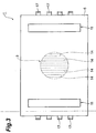
- Fig. 1 is a sectional view of an embodiment of the spectrometer in accordance with the present invention. As illustrated in Fig. 1 , this spectrometer 1 is one in which a spectroscopic unit 3 reflects and spectrally resolves light L1 having entered the inside of a package 2, so as to yield light L2, which is then detected by a photodetector 4.
- a spectroscopic unit 3 reflects and spectrally resolves light L1 having entered the inside of a package 2, so as to yield light L2, which is then detected by a photodetector 4.
- the package 2 has a rectangular parallelepiped box 5 and a rectangular plate-shaped lid 6.
- the box 5 and lid 6 are made of a light shielding or absorbing resin, examples of which include liquid-crystalline wholly aromatic polyester resins, polycarbonates, and black epoxy.
- the box 5 is provided with a recess 7 having a rectangular cross section with a flat bottom face, while the bottom face of the recess 7 is formed with a recess 8 having a rectangular cross section with a flat bottom face. Further, the bottom face of the recess 8 is provided with a recess 9 having a rectangular cross section with a flat bottom face, while the bottom face of the recess 9 is provided with a semispherical recess 10.
- the bottom face of the box 5 is provided with a pair of grooves 11.
- the semispherical recess 10 may be either spherical or aspherical.
- the inner wall face of the recess 10 includes a bottom area (first area) 12 and an area (second area) 13 surrounding the area 12.
- the areas 12, 13 are areas continuous with each other and exist on the same curved surface.
- the area 12 is formed with a plurality of grating grooves 14 arranged in a row along a predetermined direction.
- the bottom part of the recess 10 is provided with the spectroscopic unit 3 including the plurality of grating grooves 14.
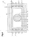
- Fig. 2 is an enlarged sectional view of the spectroscopic unit 3, while Fig. 3 is a bottom face view of the spectrometer 1.
- the spectroscopic unit 3 is constituted by the plurality of grating grooves 14 and a reflecting film 15 disposed so as to cover the grating grooves 14.
- a reflecting film 15 disposed so as to cover the grating grooves 14.
- Al, Au, or the like is vapor-deposited such as to cover the area 12 formed with the grating grooves 14, whereby the reflecting film 15 is provided.
- the spectroscopic unit 3 is a reflection type grating constructed by vapor-depositing the reflecting film 15 onto the plurality of grating grooves 14.
- Types of the grating include sawtooth blazed gratings, rectangular binary gratings, and sinusoidal holographic gratings. Regulating the size of the reflecting film 15 can adjust the optical NA.
- the reflecting film 15 is disposed in an area smaller than the area 12 formed with the grating grooves 14 so as not to generate light which is only reflected without being spectrally resolved.
- a passivation film made of SiO 2 , MgF 2 , or the like, which is not depicted, may be formed by vapor deposition or the like so as to cover the reflecting film 15 of this reflection type grating.
- the passivation film may be either larger or smaller than the area 12 formed with the grating grooves 14 as long as it covers the reflecting film 15.
- a light transmitting substrate 16 is fitted into the recess 9 so as to oppose the spectroscopic unit 3.
- the light transmitting substrate 16 is formed into a rectangular plate from any of light transmitting glass materials such as BK7, Pyrex (registered trademark), and silica, plastics, and the like, and transmits the light L1, L2 therethrough.
- the upper face of the light transmitting substrate 16 is formed with a light absorbing layer 16a having a light transmitting opening 16c for transmitting the light L1, L2 therethrough.
- Examples of materials for the light absorbing layer 16a include black resists, color resins (e.g., silicone, epoxy, acrylic, urethane, polyimide, and composite resins) containing fillers (e.g., carbon and oxides), metals and metal oxides of Cr, Co, and the like, their multilayer films, and porous ceramics and metals and metal oxides. Wiring (not depicted) is disposed on the upper or lower side of light absorbing layer 16a.
- color resins e.g., silicone, epoxy, acrylic, urethane, polyimide, and composite resins
- fillers e.g., carbon and oxides
- metals and metal oxides of Cr, Co, and the like e.g., their multilayer films, and porous ceramics and metals and metal oxides.
- Wiring (not depicted) is disposed on the upper or lower side of light absorbing layer 16a.
- Fig. 4 is a plan view of the box 5.
- the light transmitting substrate 16 and the box 5 are constructed such that a gap b between a side face of the recess 9 and a side face of the light transmitting substrate 16 in the arranging direction of the grating grooves 14 is narrower than a gap a between a side face of the recess 9 and a side face of the light transmitting substrate 16 in a direction orthogonal to the arranging direction of the grating grooves 14.
- the photodetector 4 is attached onto the light transmitting substrate 16.
- the photodetector 4 is shaped like a rectangular plate, whose surface on the spectroscopic unit 3 side is formed with a light detecting unit 21.
- the photodetector 4 is attached to the light transmitting substrate 16 by face-down bonding with bumps 18. Through the bumps 18, the photodetector 4 is electrically connected to the wiring disposed on the light transmitting substrate 16. Between the light transmitting substrate 16 and the photodetector 4, areas excluding the optical paths of the light L1, L2 are coated with a resin agent 20 covering the bumps 18 in order to improve the connection strength between the light transmitting substrate 16 and the photodetector 4.
- the light detecting unit 21 is a CCD image sensor, a PD array, a CMOS image sensor, or the like, in which a plurality of channels are arranged in a row along the arranging direction of the grating grooves 14.
- the intensity information of light at its incident position on two-dimensionally arranged pixels is subjected to line binning, so as to yield light intensity information at one-dimensional positions, and the intensity information at the one-dimensional positions is read in time series. That is, a line of pixels subjected to line binning forms one channel.
- the light detecting unit 21 is a PD array or CMOS image sensor
- intensity information of light at its incident position on one-dimensionally arranged pixels is read in time series, whereby one pixel forms one channel.
- the light detecting unit 21 is a PD array or CMOS image sensor in which pixels are arranged two-dimensionally, a line of pixels aligning in a one-dimensional arrangement direction parallel to the arranging direction of the grating grooves 14 forms one channel.
- the light detecting unit 21 is a CCD image sensor, one having a channel interval in the arrangement direction of 12.5 ⁇ m, a channel full length (length of the one-dimensional pixel row subjected to line binning) of 1 mm, and 256 arrangement channels, for example, is used for the photodetector 4.
- the photodetector 4 is also formed with a light transmitting hole 22, disposed in parallel with the light detecting unit 21 in the channel arrangement direction, for transmitting the light L1 proceeding to the spectroscopic unit 3.
- the light transmitting hole 22, which is a slit (e.g., with a length of 0.5 to 1 mm and a width of 10 to 100 ⁇ m) extending in a direction substantially orthogonal to the channel arrangement direction, is formed by etching or the like while being aligned with the light detecting unit 21 with high precision.
- Base end parts of a plurality of leads 17 embedded in the box 5 are exposed into the recess 8. Opposite end parts of the leads 17 extend to outside of the box 5.
- the base end parts of the leads 17 are electrically connected to the wiring of the light transmitting substrate 16 by wire-bonding with wires 16b.
- An electric signal generated when the light detecting unit 21 of the photodetector 4 receives the light L2 is taken out of the spectrometer 1 through the bumps 18 of the photodetector 4, the wiring of the light transmitting substrate 16, the wires 16b, and the leads 17.
- the lid 6 is fitted into the recess 7.
- the lid 6 has a light entrance hole 23 for allowing the light L1 to enter the inside of the package 2.
- a light transmitting window member 24 is attached to the light entrance hole 23.
- the window member 24 is formed by any of light transmitting glass materials such as BK7, Pyrex (registered trademark), and silica, plastics, and the like.
- the grooves 11 are located on both sides of the spectroscopic unit 3 in the arranging direction of the grating grooves 14 while extending in a direction orthogonal to the arranging direction of the grating grooves 14.
- the grooves 11 are formed integrally at the time when the box 5 is formed.
- the light L1 passes through the light entrance hole 23 of the lid 6 and the window member 24, so as to enter the inside of the package 1, and then passes through the light transmitting hole 22 of the photodetector 4 and the light transmitting substrate 16, thereby reaching the spectroscopic unit 3.
- the light L1 having reached the spectroscopic unit 3 is spectrally resolved and reflected thereby toward the light detecting unit 21 of the photodetector 4.
- the light L2 spectrally resolved and reflected by the spectroscopic unit 3 is transmitted through the light transmitting substrate 16 and detected by the light detecting unit 21 of the photodetector 4.
- the box 5 having a rectangular parallelepiped outer form with a bottom face provided with a pair of grooves 11 and the semispherical recess 10 having a bottom part integrally formed with a plurality of grating grooves 14 along a predetermined direction is prepared.
- the box 5 is also molded such that the leads 17 are embedded therein.
- Al, Au, or the like is vapor-deposited in the area formed with the grating grooves 14 in the recess 10 in the box 5, so as to provide the reflecting film 15.
- the reflecting film 15 is formed by vapor-depositing Al, Au, or the like, for example.
- the light transmitting substrate 16 provided with wiring on the upper face and the photodetector 4 formed with the light transmitting hole 22 are prepared, and the photodetector 4 and the light transmitting substrate 16 are electrically connected to each other through the wiring of the light transmitting substrate 16 and the bumps 18 of the photodetector 4. Thereafter, the resin agent 20 is applied sideways so as to cover the bumps 18, thereby bonding the light transmitting substrate 16 and the photodetector 4 to each other.
- the light transmitting substrate 16 having the photodetector 4 attached thereto is accommodated in the box 5 formed with the spectroscopic unit 3 as mentioned above.
- the light transmitting substrate 16 having the photodetector 4 attached to its upper face is fitted into the recess 9 of the box 5.
- a resin agent (not depicted) is applied between the light transmitting substrate 16 and the box 5, so as to bond the light transmitting substrate 16 to the box 5.
- the wiring of the light transmitting substrate 16 is electrically connected to the base end parts of the leads 17 through the wires 16b.
- the lid 6 is fitted into the recess 7 of the box 5 so that they are joined together airtightly, whereby the spectrometer 1 in which the photodetector 4 is accommodated in the package 2 is obtained.
- the area 13 surrounding the area 12 formed with a plurality of grating grooves 14 in the spectroscopic unit 3 is continuous with the area 12 formed with the grating grooves 14, and is formed on the same curved surface therewith. Therefore, a distortion occurring in the package 1 is dispersed by the area 13 surrounding the area 12 provided with the grating grooves 14. Hence, even when a thermal distortion is generated in the package 1, for example, positional deviations can be inhibited from occurring in the grating grooves 14, whereby the thermal dependence of spectral characteristics can be suppressed.
- the box 5 of the package 2 has a rectangular parallelepiped outer form and the recess 10 whose bottom face is a semispherical curved surface, while the area 12 and the area 13 surrounding the area 12 are formed in the bottom face of the recess. Therefore, the box 5 of the package 2 is relatively thick in the area 12 formed in the bottom face and its surrounding area 13. As a consequence, distortions are hard to occur in the area 12 formed with the grating grooves 14 in the spectroscopic unit 3 even when external forces are applied to the package 2.
- the bottom face of the box 5 is provided with a pair of grooves 11 which are located on both sides of the spectroscopic unit 3 in the arranging direction of the grating grooves 14 and extend in a direction orthogonal to the arranging direction of the grating grooves 14. Therefore, for example, sink marks occurring when resin-molding the box 5 of the package 2 are mitigated in the arranging direction of the grating grooves 14 by the pair of grooves, whereby the grating grooves 14 are further restrained from shifting their positions in this direction. If the grating grooves 14 incur a positional deviation in their arranging direction, the wavelength of light to be resolved spectrally may shift.
- the grating grooves 14 are inhibited from shifting their positions in the arranging direction of the grating grooves 14, i.e., spectral direction of light, whereby the spectral characteristic can be kept from lowering in the spectrometer 1.
- the spectrometer 1 has the light transmitting substrate 16 fitted into the recess 9 of the box 5 so as to oppose the spectroscopic unit 3, while the photodetector 4 is attached onto the light transmitting substrate 16. Therefore, the photodetector 4 can be aligned with the spectroscopic unit 3 easily with high precision in the spectrometer 1.
- the gap b between a side face of the recess 9 and a side face of the light transmitting substrate 16 in the arranging direction of the grating grooves 14 is narrower than the gap a between a side face of the recess 9 and a side face of the light transmitting substrate 16 in a direction orthogonal to the arranging direction of the grating grooves 14. Therefore, when attaching the light transmitting substrate 16 to the box 5, the light transmitting substrate 16 is accurately positioned in the arranging direction of the grating grooves 14, whereby the photodetector 4 attached onto the light transmitting substrate 16 is also precisely positioned in the arranging direction of the grating grooves 14.
- the photodetector 4 incurs a positional deviation in the arranging direction of the grating grooves 14, the wavelength of light to be detected may shift. Since the photodetector 4 can precisely be positioned in the arranging direction of the grating grooves 14, the light detection characteristic can be inhibited from lowering in the spectrometer 1. Since the gap between the side face of the recess 9 and the side face of the light transmitting substrate 16 in a direction orthogonal to the arranging direction of the grating grooves 14 is made relatively wide in the spectrometer 1, the resin agent as an adhesive is easily pushed out when mounting the light transmitting substrate 16 to the recess 9 of the box 5.
- the gap between the side face of the recess 9 and the side face of the light transmitting substrate 16 in a direction orthogonal to the arranging direction of the grating grooves 14 is made relatively wide, handling is easy. Therefore, the light transmitting substrate 16 can be mounted to the recess 9 of the box 5 easily with high precision.
- the present invention is not limited to the above-mentioned embodiment.
- the recess 10 of the box 5 illustrated in Fig. 1 is semispherical, it is not restrictive.
- the recess 10 may comprise a side face 25 which is a cylindrical curved surface (having a linear cross section) and a bottom face 26 which is a semispherical curved surface joined to the cylindrical side face 25.
- the area 12 formed with the grating grooves 14 of the spectroscopic unit 3 and the area 13 surrounding the area 12 are included in the bottom face 26 of the recess 10.
- the areas 12 and 13 are continuous with each other and disposed on the same curved surface in this case as well. Since the recess 10 can be narrowed in the portion failing to serve as optical paths for the incident light L1 and spectrally resolved light L2, the package 2 can be made smaller.
- the grooves 11 formed in the bottom face of the box 5 of the package 2 can be replaced by a cylindrical groove 27 surrounding the spectroscopic unit 3.
- sink marks occurring when resin-molding the package 10 can be mitigated not only in the arranging direction of the grating grooves 14 but also in a direction orthogonal to the arranging direction of the grating grooves 14. This can inhibit the grating grooves 14 from shifting their positions in a direction orthogonal to their arranging direction.
- the present invention can provide a spectrometer which can inhibit positional deviations from occurring in a grating groove even when distortions are generated in the package.
Landscapes
- Physics & Mathematics (AREA)
- Spectroscopy & Molecular Physics (AREA)
- General Physics & Mathematics (AREA)
- Optics & Photonics (AREA)
- Spectrometry And Color Measurement (AREA)
Applications Claiming Priority (3)
| Application Number | Priority Date | Filing Date | Title |
|---|---|---|---|
| JP2008128687 | 2008-05-15 | ||
| JP2008311003A JP5205239B2 (ja) | 2008-05-15 | 2008-12-05 | 分光器 |
| PCT/JP2009/058669 WO2009139326A1 (ja) | 2008-05-15 | 2009-05-08 | 分光器 |
Publications (3)
| Publication Number | Publication Date |
|---|---|
| EP2287578A1 EP2287578A1 (en) | 2011-02-23 |
| EP2287578A4 EP2287578A4 (en) | 2014-05-07 |
| EP2287578B1 true EP2287578B1 (en) | 2016-09-21 |
Family
ID=41318696
Family Applications (1)
| Application Number | Title | Priority Date | Filing Date |
|---|---|---|---|
| EP09746533.0A Active EP2287578B1 (en) | 2008-05-15 | 2009-05-08 | Spectrometer |
Country Status (6)
| Country | Link |
|---|---|
| US (1) | US20110141469A1 (https=) |
| EP (1) | EP2287578B1 (https=) |
| JP (1) | JP5205239B2 (https=) |
| KR (1) | KR101635649B1 (https=) |
| CN (1) | CN101970994A (https=) |
| WO (1) | WO2009139326A1 (https=) |
Families Citing this family (33)
| Publication number | Priority date | Publication date | Assignee | Title |
|---|---|---|---|---|
| JP5205242B2 (ja) * | 2008-05-15 | 2013-06-05 | 浜松ホトニクス株式会社 | 分光器の製造方法 |
| JP2009300417A (ja) * | 2008-05-15 | 2009-12-24 | Hamamatsu Photonics Kk | 分光モジュールの製造方法及び分光モジュール |
| JP5207938B2 (ja) * | 2008-05-15 | 2013-06-12 | 浜松ホトニクス株式会社 | 分光モジュール及び分光モジュールの製造方法 |
| JP5415060B2 (ja) | 2008-05-15 | 2014-02-12 | 浜松ホトニクス株式会社 | 分光モジュール |
| JP5205241B2 (ja) | 2008-05-15 | 2013-06-05 | 浜松ホトニクス株式会社 | 分光モジュール |
| JP2009300422A (ja) * | 2008-05-15 | 2009-12-24 | Hamamatsu Photonics Kk | 分光モジュール |
| JP5335729B2 (ja) | 2010-04-01 | 2013-11-06 | 浜松ホトニクス株式会社 | 分光モジュール |
| JP5325829B2 (ja) | 2010-04-01 | 2013-10-23 | 浜松ホトニクス株式会社 | 分光モジュール |
| CN103348270B (zh) * | 2011-02-08 | 2016-08-17 | 浜松光子学株式会社 | 光学元件及其制造方法 |
| JP5825880B2 (ja) * | 2011-06-27 | 2015-12-02 | 浜松ホトニクス株式会社 | 分光モジュール |
| JP5767883B2 (ja) | 2011-07-26 | 2015-08-26 | 浜松ホトニクス株式会社 | 分光器 |
| JP5767882B2 (ja) | 2011-07-26 | 2015-08-26 | 浜松ホトニクス株式会社 | 分光器 |
| JP6061542B2 (ja) * | 2012-08-06 | 2017-01-18 | 浜松ホトニクス株式会社 | 分光器 |
| JP6234667B2 (ja) * | 2012-08-06 | 2017-11-22 | 浜松ホトニクス株式会社 | 光学素子及びその製造方法 |
| JP6068039B2 (ja) * | 2012-08-06 | 2017-01-25 | 浜松ホトニクス株式会社 | 分光器 |
| CN103017905B (zh) * | 2012-12-31 | 2016-04-20 | 深圳先进技术研究院 | 集成平面变栅距光栅和微狭缝的微型光谱仪及其制造方法 |
| JP2015106106A (ja) | 2013-12-02 | 2015-06-08 | セイコーエプソン株式会社 | 電子デバイスおよび電子機器 |
| JP6325268B2 (ja) * | 2014-02-05 | 2018-05-16 | 浜松ホトニクス株式会社 | 分光器、及び分光器の製造方法 |
| JP6395389B2 (ja) | 2014-02-05 | 2018-09-26 | 浜松ホトニクス株式会社 | 分光器 |
| JP6251073B2 (ja) | 2014-02-05 | 2017-12-20 | 浜松ホトニクス株式会社 | 分光器、及び分光器の製造方法 |
| JP6104451B1 (ja) * | 2016-12-22 | 2017-03-29 | 浜松ホトニクス株式会社 | 分光器 |
| JP1583356S (https=) * | 2017-01-25 | 2017-08-07 | ||
| JP1579484S (https=) * | 2017-01-25 | 2017-06-19 | ||
| JP1579479S (https=) * | 2017-01-25 | 2017-06-19 | ||
| JP1579616S (https=) * | 2017-01-25 | 2017-06-19 | ||
| JP1579480S (https=) * | 2017-01-25 | 2017-06-19 | ||
| JP1579485S (https=) * | 2017-01-25 | 2017-06-19 | ||
| USD843013S1 (en) * | 2017-01-25 | 2019-03-12 | Hamamatsu Photonics K.K. | Substrates for spectroscopic analysis |
| JP1579612S (https=) * | 2017-01-25 | 2017-06-19 | ||
| JP1579481S (https=) * | 2017-01-25 | 2017-06-19 | ||
| JP1579483S (https=) * | 2017-01-25 | 2017-06-19 | ||
| JP1579613S (https=) * | 2017-01-25 | 2017-06-19 | ||
| JP1579614S (https=) * | 2017-01-25 | 2017-06-19 |
Family Cites Families (49)
| Publication number | Priority date | Publication date | Assignee | Title |
|---|---|---|---|---|
| US284743A (en) * | 1883-09-11 | Feanz keoedel and william wesp | ||
| US290154A (en) * | 1883-12-11 | Victoe vidal | ||
| US75143A (en) * | 1868-03-03 | Samuel l | ||
| US290164A (en) * | 1883-12-11 | Hezekiah weight | ||
| US290155A (en) * | 1883-12-11 | Fbedeick wellmann | ||
| US4259014A (en) * | 1979-04-03 | 1981-03-31 | Princeton Applied Research Corporation | Fiber optic polychromator |
| DE3509131A1 (de) * | 1985-03-14 | 1986-09-18 | Fa. Carl Zeiss, 7920 Heidenheim | Verfahren zur justierten montage der optischen bauteile eines optischen geraetes |
| DE4038638A1 (de) * | 1990-12-04 | 1992-06-11 | Zeiss Carl Fa | Diodenzeilen-spektrometer |
| JPH04287001A (ja) * | 1991-03-15 | 1992-10-12 | Sekinosu Kk | 光回折格子の製造方法 |
| JPH08145794A (ja) | 1994-11-17 | 1996-06-07 | Shimadzu Corp | 分光器 |
| US5995221A (en) * | 1997-02-28 | 1999-11-30 | Instruments S.A., Inc. | Modified concentric spectrograph |
| US6303934B1 (en) * | 1997-04-10 | 2001-10-16 | James T. Daly | Monolithic infrared spectrometer apparatus and methods |
| DE19717014A1 (de) * | 1997-04-23 | 1998-10-29 | Inst Mikrotechnik Mainz Gmbh | Verfahren und Form zur Herstellung miniaturisierter Formenkörper |
| EP0942267B1 (de) * | 1998-03-11 | 2006-08-30 | Gretag-Macbeth AG | Spektrometer |
| US6249346B1 (en) * | 1998-12-21 | 2001-06-19 | Xerox Corporation | Monolithic spectrophotometer |
| US6608679B1 (en) * | 1998-12-21 | 2003-08-19 | Xerox Corporation | Spectrophotometric analysis of input light |
| EP1041372B1 (de) | 1999-04-01 | 2006-03-01 | Gretag-Macbeth AG | Spektrometer |
| US6538736B1 (en) * | 1999-12-01 | 2003-03-25 | Hach Company | Concentric spectrometer with mitigation of internal specular reflections |
| WO2002004901A1 (en) * | 2000-07-11 | 2002-01-17 | Adc Telecommunications, Inc. | Monitoring apparatus for optical transmission systems |
| WO2002010698A1 (en) * | 2000-07-28 | 2002-02-07 | Otsuka Electronics Co., Ltd. | Light spectrum detecting apparatus |
| US6657723B2 (en) * | 2000-12-13 | 2003-12-02 | International Business Machines Corporation | Multimode planar spectrographs for wavelength demultiplexing and methods of fabrication |
| JP4221965B2 (ja) * | 2002-07-22 | 2009-02-12 | 日立電線株式会社 | 回折格子、波長合分波器及びこれらを用いた波長多重信号光伝送モジュール |
| US6885107B2 (en) * | 2002-08-29 | 2005-04-26 | Micron Technology, Inc. | Flip-chip image sensor packages and methods of fabrication |
| WO2004027493A1 (ja) * | 2002-09-20 | 2004-04-01 | Nippon Sheet Glass Company, Limited | 回折格子を用いた分光装置 |
| DE10304312A1 (de) * | 2003-02-04 | 2004-08-12 | Carl Zeiss Jena Gmbh | Kompakt-Spektrometer |
| JP2004309146A (ja) * | 2003-04-02 | 2004-11-04 | Olympus Corp | 分光光度計 |
| JP4409860B2 (ja) * | 2003-05-28 | 2010-02-03 | 浜松ホトニクス株式会社 | 光検出器を用いた分光器 |
| US7283233B1 (en) * | 2004-03-20 | 2007-10-16 | Seng-Tiong Ho | Curved grating spectrometer with very high wavelength resolution |
| US7623235B2 (en) * | 2004-03-20 | 2009-11-24 | Seng-Tiong Ho | Curved grating spectrometer with very high wavelength resolution |
| EP1779074A2 (en) * | 2004-07-26 | 2007-05-02 | Danmarks Tekniske Universitet | On-chip spectroscopy |
| JP2006322841A (ja) * | 2005-05-19 | 2006-11-30 | Shimadzu Corp | 分光測定方法及び分光光度計 |
| US7330258B2 (en) * | 2005-05-27 | 2008-02-12 | Innovative Technical Solutions, Inc. | Spectrometer designs |
| US7289220B2 (en) * | 2005-10-14 | 2007-10-30 | Board Of Regents, The University Of Texas System | Broadband cavity spectrometer apparatus and method for determining the path length of an optical structure |
| US7697137B2 (en) * | 2006-04-28 | 2010-04-13 | Corning Incorporated | Monolithic Offner spectrometer |
| JP4644632B2 (ja) | 2006-05-29 | 2011-03-02 | 松下金属工業株式会社 | ホッパー型コイン払出し装置のコイン払出し用可動誘導体 |
| EP1882916A1 (en) * | 2006-07-20 | 2008-01-30 | Interuniversitair Microelektronica Centrum | Compact catadioptric spectrometer |
| JP4905193B2 (ja) * | 2007-03-16 | 2012-03-28 | コニカミノルタセンシング株式会社 | 凹面回折ミラー及びこれを用いた分光装置 |
| EP2063238B1 (en) * | 2007-06-08 | 2018-08-22 | Hamamatsu Photonics K.K. | Spectroscope |
| US8068223B2 (en) * | 2007-06-08 | 2011-11-29 | Hamamatsu Photonics K.K. | Spectroscopic module |
| TWI342862B (en) * | 2008-01-31 | 2011-06-01 | Univ Nat Taiwan | Method of micro/nano imprinting |
| CN102628711B (zh) * | 2008-03-04 | 2016-01-20 | 浜松光子学株式会社 | 分光模块 |
| JP5111163B2 (ja) * | 2008-03-04 | 2012-12-26 | 浜松ホトニクス株式会社 | 分光器 |
| JP5205243B2 (ja) * | 2008-05-15 | 2013-06-05 | 浜松ホトニクス株式会社 | 分光器 |
| JP5411778B2 (ja) * | 2009-04-30 | 2014-02-12 | キヤノン株式会社 | 分光測色装置、およびそれを用いた画像形成装置 |
| JP2010261767A (ja) * | 2009-05-01 | 2010-11-18 | Canon Inc | 分光装置及びそれを有する画像形成装置 |
| JP5669434B2 (ja) * | 2009-05-09 | 2015-02-12 | キヤノン株式会社 | 回折素子及び回折素子の製造方法及びそれを用いた分光器 |
| JP5421684B2 (ja) * | 2009-07-29 | 2014-02-19 | キヤノン株式会社 | 回折光学素子、それを用いた分光測色装置および画像形成装置 |
| DE102009046831B4 (de) * | 2009-11-18 | 2015-02-12 | Fraunhofer-Gesellschaft zur Förderung der angewandten Forschung e.V. | Strahlungserzeugungsvorrichtung zum Erzeugen einer elektromagnetischen Strahlung mit einer einstellbaren spektralen Zusammensetzung und Verfahren zur Herstellung derselben |
| JP5335729B2 (ja) * | 2010-04-01 | 2013-11-06 | 浜松ホトニクス株式会社 | 分光モジュール |
-
2008
- 2008-12-05 JP JP2008311003A patent/JP5205239B2/ja active Active
-
2009
- 2009-05-08 US US12/992,412 patent/US20110141469A1/en not_active Abandoned
- 2009-05-08 WO PCT/JP2009/058669 patent/WO2009139326A1/ja not_active Ceased
- 2009-05-08 KR KR1020107015312A patent/KR101635649B1/ko active Active
- 2009-05-08 CN CN2009801089043A patent/CN101970994A/zh active Pending
- 2009-05-08 EP EP09746533.0A patent/EP2287578B1/en active Active
Also Published As
| Publication number | Publication date |
|---|---|
| JP5205239B2 (ja) | 2013-06-05 |
| EP2287578A4 (en) | 2014-05-07 |
| KR20110008004A (ko) | 2011-01-25 |
| JP2009300414A (ja) | 2009-12-24 |
| EP2287578A1 (en) | 2011-02-23 |
| US20110141469A1 (en) | 2011-06-16 |
| WO2009139326A1 (ja) | 2009-11-19 |
| KR101635649B1 (ko) | 2016-07-08 |
| CN101970994A (zh) | 2011-02-09 |
Similar Documents
| Publication | Publication Date | Title |
|---|---|---|
| EP2287578B1 (en) | Spectrometer | |
| EP2287579B1 (en) | Method for manufacturing spectrometer | |
| EP2116827B1 (en) | Spectroscope | |
| US8604412B2 (en) | Spectral module and method for manufacturing spectral module | |
| EP3358320B1 (en) | Light detection device | |
| JP5512961B2 (ja) | 分光モジュール及びその製造方法 | |
| EP2287574B1 (en) | Spectral module | |
| EP3605043B1 (en) | Light detecting device | |
| WO2012114632A1 (ja) | 分光モジュール | |
| WO2014024718A1 (ja) | 分光器 |
Legal Events
| Date | Code | Title | Description |
|---|---|---|---|
| PUAI | Public reference made under article 153(3) epc to a published international application that has entered the european phase |
Free format text: ORIGINAL CODE: 0009012 |
|
| 17P | Request for examination filed |
Effective date: 20101201 |
|
| AK | Designated contracting states |
Kind code of ref document: A1 Designated state(s): AT BE BG CH CY CZ DE DK EE ES FI FR GB GR HR HU IE IS IT LI LT LU LV MC MK MT NL NO PL PT RO SE SI SK TR |
|
| AX | Request for extension of the european patent |
Extension state: AL BA RS |
|
| DAX | Request for extension of the european patent (deleted) | ||
| RIC1 | Information provided on ipc code assigned before grant |
Ipc: G01J 3/18 20060101AFI20140327BHEP Ipc: G02B 7/00 20060101ALI20140327BHEP Ipc: G01J 3/02 20060101ALI20140327BHEP |
|
| A4 | Supplementary search report drawn up and despatched |
Effective date: 20140404 |
|
| 17Q | First examination report despatched |
Effective date: 20150415 |
|
| GRAP | Despatch of communication of intention to grant a patent |
Free format text: ORIGINAL CODE: EPIDOSNIGR1 |
|
| INTG | Intention to grant announced |
Effective date: 20151021 |
|
| GRAP | Despatch of communication of intention to grant a patent |
Free format text: ORIGINAL CODE: EPIDOSNIGR1 |
|
| INTG | Intention to grant announced |
Effective date: 20160615 |
|
| GRAS | Grant fee paid |
Free format text: ORIGINAL CODE: EPIDOSNIGR3 |
|
| GRAA | (expected) grant |
Free format text: ORIGINAL CODE: 0009210 |
|
| AK | Designated contracting states |
Kind code of ref document: B1 Designated state(s): AT BE BG CH CY CZ DE DK EE ES FI FR GB GR HR HU IE IS IT LI LT LU LV MC MK MT NL NO PL PT RO SE SI SK TR |
|
| REG | Reference to a national code |
Ref country code: GB Ref legal event code: FG4D |
|
| REG | Reference to a national code |
Ref country code: CH Ref legal event code: EP |
|
| REG | Reference to a national code |
Ref country code: AT Ref legal event code: REF Ref document number: 831427 Country of ref document: AT Kind code of ref document: T Effective date: 20161015 |
|
| REG | Reference to a national code |
Ref country code: IE Ref legal event code: FG4D |
|
| REG | Reference to a national code |
Ref country code: DE Ref legal event code: R096 Ref document number: 602009041275 Country of ref document: DE |
|
| REG | Reference to a national code |
Ref country code: LT Ref legal event code: MG4D Ref country code: NL Ref legal event code: MP Effective date: 20160921 |
|
| PG25 | Lapsed in a contracting state [announced via postgrant information from national office to epo] |
Ref country code: FI Free format text: LAPSE BECAUSE OF FAILURE TO SUBMIT A TRANSLATION OF THE DESCRIPTION OR TO PAY THE FEE WITHIN THE PRESCRIBED TIME-LIMIT Effective date: 20160921 Ref country code: LT Free format text: LAPSE BECAUSE OF FAILURE TO SUBMIT A TRANSLATION OF THE DESCRIPTION OR TO PAY THE FEE WITHIN THE PRESCRIBED TIME-LIMIT Effective date: 20160921 Ref country code: NO Free format text: LAPSE BECAUSE OF FAILURE TO SUBMIT A TRANSLATION OF THE DESCRIPTION OR TO PAY THE FEE WITHIN THE PRESCRIBED TIME-LIMIT Effective date: 20161221 |
|
| REG | Reference to a national code |
Ref country code: AT Ref legal event code: MK05 Ref document number: 831427 Country of ref document: AT Kind code of ref document: T Effective date: 20160921 |
|
| PG25 | Lapsed in a contracting state [announced via postgrant information from national office to epo] |
Ref country code: SE Free format text: LAPSE BECAUSE OF FAILURE TO SUBMIT A TRANSLATION OF THE DESCRIPTION OR TO PAY THE FEE WITHIN THE PRESCRIBED TIME-LIMIT Effective date: 20160921 Ref country code: NL Free format text: LAPSE BECAUSE OF FAILURE TO SUBMIT A TRANSLATION OF THE DESCRIPTION OR TO PAY THE FEE WITHIN THE PRESCRIBED TIME-LIMIT Effective date: 20160921 Ref country code: GR Free format text: LAPSE BECAUSE OF FAILURE TO SUBMIT A TRANSLATION OF THE DESCRIPTION OR TO PAY THE FEE WITHIN THE PRESCRIBED TIME-LIMIT Effective date: 20161222 Ref country code: LV Free format text: LAPSE BECAUSE OF FAILURE TO SUBMIT A TRANSLATION OF THE DESCRIPTION OR TO PAY THE FEE WITHIN THE PRESCRIBED TIME-LIMIT Effective date: 20160921 |
|
| REG | Reference to a national code |
Ref country code: FR Ref legal event code: PLFP Year of fee payment: 9 |
|
| PG25 | Lapsed in a contracting state [announced via postgrant information from national office to epo] |
Ref country code: EE Free format text: LAPSE BECAUSE OF FAILURE TO SUBMIT A TRANSLATION OF THE DESCRIPTION OR TO PAY THE FEE WITHIN THE PRESCRIBED TIME-LIMIT Effective date: 20160921 Ref country code: RO Free format text: LAPSE BECAUSE OF FAILURE TO SUBMIT A TRANSLATION OF THE DESCRIPTION OR TO PAY THE FEE WITHIN THE PRESCRIBED TIME-LIMIT Effective date: 20160921 |
|
| PG25 | Lapsed in a contracting state [announced via postgrant information from national office to epo] |
Ref country code: BE Free format text: LAPSE BECAUSE OF FAILURE TO SUBMIT A TRANSLATION OF THE DESCRIPTION OR TO PAY THE FEE WITHIN THE PRESCRIBED TIME-LIMIT Effective date: 20160921 Ref country code: SK Free format text: LAPSE BECAUSE OF FAILURE TO SUBMIT A TRANSLATION OF THE DESCRIPTION OR TO PAY THE FEE WITHIN THE PRESCRIBED TIME-LIMIT Effective date: 20160921 Ref country code: PL Free format text: LAPSE BECAUSE OF FAILURE TO SUBMIT A TRANSLATION OF THE DESCRIPTION OR TO PAY THE FEE WITHIN THE PRESCRIBED TIME-LIMIT Effective date: 20160921 Ref country code: IS Free format text: LAPSE BECAUSE OF FAILURE TO SUBMIT A TRANSLATION OF THE DESCRIPTION OR TO PAY THE FEE WITHIN THE PRESCRIBED TIME-LIMIT Effective date: 20170121 Ref country code: BG Free format text: LAPSE BECAUSE OF FAILURE TO SUBMIT A TRANSLATION OF THE DESCRIPTION OR TO PAY THE FEE WITHIN THE PRESCRIBED TIME-LIMIT Effective date: 20161221 Ref country code: CZ Free format text: LAPSE BECAUSE OF FAILURE TO SUBMIT A TRANSLATION OF THE DESCRIPTION OR TO PAY THE FEE WITHIN THE PRESCRIBED TIME-LIMIT Effective date: 20160921 Ref country code: AT Free format text: LAPSE BECAUSE OF FAILURE TO SUBMIT A TRANSLATION OF THE DESCRIPTION OR TO PAY THE FEE WITHIN THE PRESCRIBED TIME-LIMIT Effective date: 20160921 Ref country code: PT Free format text: LAPSE BECAUSE OF FAILURE TO SUBMIT A TRANSLATION OF THE DESCRIPTION OR TO PAY THE FEE WITHIN THE PRESCRIBED TIME-LIMIT Effective date: 20170123 Ref country code: ES Free format text: LAPSE BECAUSE OF FAILURE TO SUBMIT A TRANSLATION OF THE DESCRIPTION OR TO PAY THE FEE WITHIN THE PRESCRIBED TIME-LIMIT Effective date: 20160921 |
|
| REG | Reference to a national code |
Ref country code: DE Ref legal event code: R097 Ref document number: 602009041275 Country of ref document: DE |
|
| PG25 | Lapsed in a contracting state [announced via postgrant information from national office to epo] |
Ref country code: IT Free format text: LAPSE BECAUSE OF FAILURE TO SUBMIT A TRANSLATION OF THE DESCRIPTION OR TO PAY THE FEE WITHIN THE PRESCRIBED TIME-LIMIT Effective date: 20160921 |
|
| PLBE | No opposition filed within time limit |
Free format text: ORIGINAL CODE: 0009261 |
|
| STAA | Information on the status of an ep patent application or granted ep patent |
Free format text: STATUS: NO OPPOSITION FILED WITHIN TIME LIMIT |
|
| PG25 | Lapsed in a contracting state [announced via postgrant information from national office to epo] |
Ref country code: DK Free format text: LAPSE BECAUSE OF FAILURE TO SUBMIT A TRANSLATION OF THE DESCRIPTION OR TO PAY THE FEE WITHIN THE PRESCRIBED TIME-LIMIT Effective date: 20160921 |
|
| 26N | No opposition filed |
Effective date: 20170622 |
|
| PG25 | Lapsed in a contracting state [announced via postgrant information from national office to epo] |
Ref country code: LU Free format text: LAPSE BECAUSE OF NON-PAYMENT OF DUE FEES Effective date: 20170531 |
|
| PG25 | Lapsed in a contracting state [announced via postgrant information from national office to epo] |
Ref country code: SI Free format text: LAPSE BECAUSE OF FAILURE TO SUBMIT A TRANSLATION OF THE DESCRIPTION OR TO PAY THE FEE WITHIN THE PRESCRIBED TIME-LIMIT Effective date: 20160921 |
|
| PG25 | Lapsed in a contracting state [announced via postgrant information from national office to epo] |
Ref country code: MC Free format text: LAPSE BECAUSE OF FAILURE TO SUBMIT A TRANSLATION OF THE DESCRIPTION OR TO PAY THE FEE WITHIN THE PRESCRIBED TIME-LIMIT Effective date: 20160921 |
|
| REG | Reference to a national code |
Ref country code: IE Ref legal event code: MM4A |
|
| PG25 | Lapsed in a contracting state [announced via postgrant information from national office to epo] |
Ref country code: LU Free format text: LAPSE BECAUSE OF NON-PAYMENT OF DUE FEES Effective date: 20170508 |
|
| REG | Reference to a national code |
Ref country code: FR Ref legal event code: PLFP Year of fee payment: 10 |
|
| PG25 | Lapsed in a contracting state [announced via postgrant information from national office to epo] |
Ref country code: IE Free format text: LAPSE BECAUSE OF NON-PAYMENT OF DUE FEES Effective date: 20170508 |
|
| PG25 | Lapsed in a contracting state [announced via postgrant information from national office to epo] |
Ref country code: MT Free format text: LAPSE BECAUSE OF NON-PAYMENT OF DUE FEES Effective date: 20170508 |
|
| PG25 | Lapsed in a contracting state [announced via postgrant information from national office to epo] |
Ref country code: HU Free format text: LAPSE BECAUSE OF FAILURE TO SUBMIT A TRANSLATION OF THE DESCRIPTION OR TO PAY THE FEE WITHIN THE PRESCRIBED TIME-LIMIT; INVALID AB INITIO Effective date: 20090508 |
|
| PG25 | Lapsed in a contracting state [announced via postgrant information from national office to epo] |
Ref country code: CY Free format text: LAPSE BECAUSE OF NON-PAYMENT OF DUE FEES Effective date: 20160921 |
|
| PG25 | Lapsed in a contracting state [announced via postgrant information from national office to epo] |
Ref country code: MK Free format text: LAPSE BECAUSE OF FAILURE TO SUBMIT A TRANSLATION OF THE DESCRIPTION OR TO PAY THE FEE WITHIN THE PRESCRIBED TIME-LIMIT Effective date: 20160921 |
|
| PG25 | Lapsed in a contracting state [announced via postgrant information from national office to epo] |
Ref country code: TR Free format text: LAPSE BECAUSE OF FAILURE TO SUBMIT A TRANSLATION OF THE DESCRIPTION OR TO PAY THE FEE WITHIN THE PRESCRIBED TIME-LIMIT Effective date: 20160921 |
|
| PG25 | Lapsed in a contracting state [announced via postgrant information from national office to epo] |
Ref country code: HR Free format text: LAPSE BECAUSE OF FAILURE TO SUBMIT A TRANSLATION OF THE DESCRIPTION OR TO PAY THE FEE WITHIN THE PRESCRIBED TIME-LIMIT Effective date: 20160921 |
|
| REG | Reference to a national code |
Ref country code: FR Ref legal event code: PLFP Year of fee payment: 15 |
|
| P01 | Opt-out of the competence of the unified patent court (upc) registered |
Effective date: 20230517 |
|
| PGFP | Annual fee paid to national office [announced via postgrant information from national office to epo] |
Ref country code: GB Payment date: 20250327 Year of fee payment: 17 |
|
| PGFP | Annual fee paid to national office [announced via postgrant information from national office to epo] |
Ref country code: DE Payment date: 20250402 Year of fee payment: 17 |
|
| PGFP | Annual fee paid to national office [announced via postgrant information from national office to epo] |
Ref country code: FR Payment date: 20250401 Year of fee payment: 17 |
|
| PGFP | Annual fee paid to national office [announced via postgrant information from national office to epo] |
Ref country code: CH Payment date: 20250601 Year of fee payment: 17 |