EP2287574A1 - Spectral module - Google Patents
Spectral module Download PDFInfo
- Publication number
- EP2287574A1 EP2287574A1 EP09746522A EP09746522A EP2287574A1 EP 2287574 A1 EP2287574 A1 EP 2287574A1 EP 09746522 A EP09746522 A EP 09746522A EP 09746522 A EP09746522 A EP 09746522A EP 2287574 A1 EP2287574 A1 EP 2287574A1
- Authority
- EP
- European Patent Office
- Prior art keywords
- unit
- photodetector
- substrate
- light
- recess
- Prior art date
- Legal status (The legal status is an assumption and is not a legal conclusion. Google has not performed a legal analysis and makes no representation as to the accuracy of the status listed.)
- Granted
Links
Images








Classifications
-
- G—PHYSICS
- G01—MEASURING; TESTING
- G01J—MEASUREMENT OF INTENSITY, VELOCITY, SPECTRAL CONTENT, POLARISATION, PHASE OR PULSE CHARACTERISTICS OF INFRARED, VISIBLE OR ULTRAVIOLET LIGHT; COLORIMETRY; RADIATION PYROMETRY
- G01J3/00—Spectrometry; Spectrophotometry; Monochromators; Measuring colours
- G01J3/02—Details
-
- G—PHYSICS
- G01—MEASURING; TESTING
- G01J—MEASUREMENT OF INTENSITY, VELOCITY, SPECTRAL CONTENT, POLARISATION, PHASE OR PULSE CHARACTERISTICS OF INFRARED, VISIBLE OR ULTRAVIOLET LIGHT; COLORIMETRY; RADIATION PYROMETRY
- G01J3/00—Spectrometry; Spectrophotometry; Monochromators; Measuring colours
- G01J3/02—Details
- G01J3/0205—Optical elements not provided otherwise, e.g. optical manifolds, diffusers, windows
- G01J3/0208—Optical elements not provided otherwise, e.g. optical manifolds, diffusers, windows using focussing or collimating elements, e.g. lenses or mirrors; performing aberration correction
-
- G—PHYSICS
- G01—MEASURING; TESTING
- G01J—MEASUREMENT OF INTENSITY, VELOCITY, SPECTRAL CONTENT, POLARISATION, PHASE OR PULSE CHARACTERISTICS OF INFRARED, VISIBLE OR ULTRAVIOLET LIGHT; COLORIMETRY; RADIATION PYROMETRY
- G01J3/00—Spectrometry; Spectrophotometry; Monochromators; Measuring colours
- G01J3/02—Details
- G01J3/0205—Optical elements not provided otherwise, e.g. optical manifolds, diffusers, windows
- G01J3/0243—Optical elements not provided otherwise, e.g. optical manifolds, diffusers, windows having a through-hole enabling the optical element to fulfil an additional optical function, e.g. a mirror or grating having a throughhole for a light collecting or light injecting optical fiber
-
- G—PHYSICS
- G01—MEASURING; TESTING
- G01J—MEASUREMENT OF INTENSITY, VELOCITY, SPECTRAL CONTENT, POLARISATION, PHASE OR PULSE CHARACTERISTICS OF INFRARED, VISIBLE OR ULTRAVIOLET LIGHT; COLORIMETRY; RADIATION PYROMETRY
- G01J3/00—Spectrometry; Spectrophotometry; Monochromators; Measuring colours
- G01J3/02—Details
- G01J3/0256—Compact construction
-
- G—PHYSICS
- G01—MEASURING; TESTING
- G01J—MEASUREMENT OF INTENSITY, VELOCITY, SPECTRAL CONTENT, POLARISATION, PHASE OR PULSE CHARACTERISTICS OF INFRARED, VISIBLE OR ULTRAVIOLET LIGHT; COLORIMETRY; RADIATION PYROMETRY
- G01J3/00—Spectrometry; Spectrophotometry; Monochromators; Measuring colours
- G01J3/02—Details
- G01J3/0256—Compact construction
- G01J3/0259—Monolithic
-
- G—PHYSICS
- G01—MEASURING; TESTING
- G01J—MEASUREMENT OF INTENSITY, VELOCITY, SPECTRAL CONTENT, POLARISATION, PHASE OR PULSE CHARACTERISTICS OF INFRARED, VISIBLE OR ULTRAVIOLET LIGHT; COLORIMETRY; RADIATION PYROMETRY
- G01J3/00—Spectrometry; Spectrophotometry; Monochromators; Measuring colours
- G01J3/02—Details
- G01J3/0286—Constructional arrangements for compensating for fluctuations caused by temperature, humidity or pressure, or using cooling or temperature stabilization of parts of the device; Controlling the atmosphere inside a spectrometer, e.g. vacuum
-
- G—PHYSICS
- G01—MEASURING; TESTING
- G01J—MEASUREMENT OF INTENSITY, VELOCITY, SPECTRAL CONTENT, POLARISATION, PHASE OR PULSE CHARACTERISTICS OF INFRARED, VISIBLE OR ULTRAVIOLET LIGHT; COLORIMETRY; RADIATION PYROMETRY
- G01J3/00—Spectrometry; Spectrophotometry; Monochromators; Measuring colours
- G01J3/02—Details
- G01J3/0297—Constructional arrangements for removing other types of optical noise or for performing calibration
-
- G—PHYSICS
- G02—OPTICS
- G02B—OPTICAL ELEMENTS, SYSTEMS OR APPARATUS
- G02B27/00—Optical systems or apparatus not provided for by any of the groups G02B1/00 - G02B26/00, G02B30/00
- G02B27/42—Diffraction optics, i.e. systems including a diffractive element being designed for providing a diffractive effect
- G02B27/4233—Diffraction optics, i.e. systems including a diffractive element being designed for providing a diffractive effect having a diffractive element [DOE] contributing to a non-imaging application
- G02B27/4244—Diffraction optics, i.e. systems including a diffractive element being designed for providing a diffractive effect having a diffractive element [DOE] contributing to a non-imaging application in wavelength selecting devices
-
- G—PHYSICS
- G02—OPTICS
- G02B—OPTICAL ELEMENTS, SYSTEMS OR APPARATUS
- G02B5/00—Optical elements other than lenses
- G02B5/18—Diffraction gratings
- G02B5/1814—Diffraction gratings structurally combined with one or more further optical elements, e.g. lenses, mirrors, prisms or other diffraction gratings
-
- G—PHYSICS
- G02—OPTICS
- G02B—OPTICAL ELEMENTS, SYSTEMS OR APPARATUS
- G02B5/00—Optical elements other than lenses
- G02B5/18—Diffraction gratings
- G02B5/1847—Manufacturing methods
- G02B5/1852—Manufacturing methods using mechanical means, e.g. ruling with diamond tool, moulding
-
- G—PHYSICS
- G02—OPTICS
- G02B—OPTICAL ELEMENTS, SYSTEMS OR APPARATUS
- G02B5/00—Optical elements other than lenses
- G02B5/18—Diffraction gratings
- G02B5/1861—Reflection gratings characterised by their structure, e.g. step profile, contours of substrate or grooves, pitch variations, materials
-
- G—PHYSICS
- G02—OPTICS
- G02B—OPTICAL ELEMENTS, SYSTEMS OR APPARATUS
- G02B7/00—Mountings, adjusting means, or light-tight connections, for optical elements
- G02B7/02—Mountings, adjusting means, or light-tight connections, for optical elements for lenses
- G02B7/025—Mountings, adjusting means, or light-tight connections, for optical elements for lenses using glue
-
- G—PHYSICS
- G01—MEASURING; TESTING
- G01J—MEASUREMENT OF INTENSITY, VELOCITY, SPECTRAL CONTENT, POLARISATION, PHASE OR PULSE CHARACTERISTICS OF INFRARED, VISIBLE OR ULTRAVIOLET LIGHT; COLORIMETRY; RADIATION PYROMETRY
- G01J3/00—Spectrometry; Spectrophotometry; Monochromators; Measuring colours
- G01J3/12—Generating the spectrum; Monochromators
- G01J2003/1213—Filters in general, e.g. dichroic, band
Definitions
- the present invention relates to a spectral module for spectrally resolving and detecting light.
- Patent Literature 1 discloses a spectral module having a block-shaped support which is a biconvex lens, in which one convex surface of the support is provided with a spectroscopic unit such as a diffraction grating, while a photodetector such as a photodiode is disposed on the other convex surface side of the support.
- the spectral module described in Patent Literature 1 necessitates so-called active alignment in which, while the light spectrally resolved by the spectroscopic unit is received by the photodetector, the spectroscopic unit is moved relative to the photodetector, and the spectroscopic unit and the photodetector are positioned with respect to each other according to the light-receiving state of the photodetector.
- active alignment is problematic in that an operation for assembling the spectral module takes a long time.
- the spectral module in accordance with the present invention comprises a substrate for transmitting light incident thereon from one surface; a light transmitting unit, disposed on the other surface side of the substrate, for transmitting the light incident on the substrate; a spectroscopic unit, formed with the light transmitting unit, for reflecting and spectrally resolving the light incident on the light transmitting unit; and a photodetector, disposed on the one surface side of the substrate, for detecting the light spectrally resolved by the spectroscopic unit; wherein the other surface is provided with a recess, adapted to mate with the light transmitting unit through an optical resin agent, having a predetermined positional relationship with a reference unit for positioning the photodetector with respect to the substrate; wherein the recess is provided with a first mating section adapted to mate with the light transmitting unit in an extending direction of a grating groove of the spectroscopic unit and a second mating section adapted to
- the spectroscopic unit and the light transmitting unit are positioned with respect to the substrate when the light transmitting unit formed with the spectroscopic unit is simply mated with the recess.
- the photodetector is positioned with respect to the substrate by the reference unit, whereby alignment is achieved between the spectroscopic unit and the photodetector.
- the gap between the mating section and the light transmitting unit in a direction substantially orthogonal to the extending direction of the grating groove of the spectroscopic unit is smaller than that between the mating section and the light transmitting unit in the extending direction of the grating groove of the spectroscopic unit.
- the recess has a side wall including a spaced section deviating from the first and second mating sections and the light transmitting unit.
- a structure can release the excess of resin and air more effectively through the gap between the light transmitting unit and the spaced section when bonding the light transmitting unit to the substrate with the optical resin agent. This can suppress unevenness in the resin agent and occurrence of bubbles between the light transmitting unit and the substrate, thereby making it possible to mount the light transmitting unit more precisely to the substrate.
- the spaced section comprises a plurality of sections disposed so as to surround the light transmitting unit.
- This structure can release the excess of resin and air through a plurality of gaps more efficiently when bonding the light transmitting unit to the substrate with the optical resin agent.
- the spectral module in accordance with the present invention comprises a substrate for transmitting light incident thereon from one surface; a light transmitting unit, disposed on the other surface side of the substrate, for transmitting the light incident on the substrate; a spectroscopic unit, formed with the light transmitting unit, for reflecting and spectrally resolving the light incident on the light transmitting unit; and a photodetector, disposed on the one surface side of the substrate, for detecting the light spectrally resolved by the spectroscopic unit; wherein the other surface is provided with a recess having a predetermined positional relationship with a reference unit for positioning the photodetector with respect to the substrate; and wherein the light transmitting unit is mated with the recess.
- the spectroscopic unit and the light transmitting unit are positioned with respect to the substrate when the light transmitting unit formed with the spectroscopic unit is simply mated with the recess.
- the photodetector is positioned with respect to the substrate by the reference unit, whereby alignment is achieved between the spectroscopic unit and the photodetector.
- the spectral module in accordance with the present invention comprises a main unit for transmitting light incident thereon from one surface side; a spectroscopic unit, formed with the main unit, for reflecting and spectrally resolving the light incident on the main unit; and a photodetector, disposed on the one surface side of the main unit, for detecting the light spectrally resolved by the spectroscopic unit; wherein the one surface is provided with a recess, adapted to mate with the photodetector through an optical resin agent, having a predetermined positional relationship with a reference unit for positioning the spectroscopic unit with respect to the main unit; wherein the recess is provided with a third mating section adapted to mate with the photodetector in an extending direction of a grating groove of the spectroscopic unit and a fourth mating section adapted to mate with the photodetector in a direction substantially orthogonal to the extending direction of the grating groove; and wherein the one surface is provided
- the photodetector is positioned with respect to the main unit when the photodetector is simply mated with the recess.
- the spectroscopic unit is positioned with respect to the main unit by the reference unit, whereby alignment is achieved between the spectroscopic unit and the photodetector.
- the gap between the mating section and the photodetector in a direction substantially orthogonal to the extending direction of the grating groove of the spectroscopic unit is smaller than that between the mating section and the photodetector in the extending direction of the grating groove of the spectroscopic unit.
- an excess of resin and air can effectively be released, since the gap between the photodetector and the mating section is formed greater in the extending direction of the grating groove.
- This spectral module thus achieves so-called passive alignment, which can make it easy to assemble while keeping reliability.
- the photodetector has an elongated form such as to be longer in a direction substantially orthogonal to the extending direction of the grating groove than in the extending direction of the grating groove.
- This structure makes the gap between the mating section and the photodetector longer and the distance to the gap shorter in the extending direction of the grating groove than in a direction substantially orthogonal to the extending direction of the grating groove, whereby the excess of resin and air can be moved efficiently to the gap.
- the photodetector projects from the one surface while mating with the recess.
- This structure can not only make it easier to mate the photodetector with the recess disposed in one surface of the substrate, but also reliably press the photodetector against the bottom face of the recess, thereby securely releasing the excess of resin and air.
- the photodetector is provided with a light transmitting hole for transmitting light proceeding to the spectroscopic unit.
- This structure can achieve passive alignment of the light transmitting hole with respect to the spectroscopic unit and photodetector.
- the present invention makes it possible to assemble a spectral module easily while keeping the reliability of the spectral module.
- Fig. 1 is a plan view of the first embodiment of the spectral module in accordance with the present invention
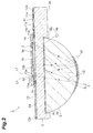
- Fig. 2 is a sectional view taken along the line II-II of Fig. 1
- this spectral module 1 comprises a substrate 2 for transmitting light L1 incident thereon from its front face (one surface) 2a, a lens unit (light transmitting unit) 3 for transmitting the light L1 incident on the substrate 2, a spectroscopic unit 4 for reflecting and spectrally resolving the light L1 incident on the lens unit 3, and a photodetector 5 for detecting light L2 reflected by the spectroscopic unit 4.
- the spectral module 1 is a microspectral module which spectrally resolves the light L1 into the light L2 corresponding to a plurality of wavelengths with the spectroscopic unit 4 and detects the light L2 with the photodetector 5, thereby measuring the wavelength distribution, strength of a specific wavelength component, and the like of the light L1.
- the substrate 2 is formed into an rectangular plate (e.g. with a full length of 15 to 20 mm, a full width of 11 to 12 mm, and a thickness of 1 to 3 mm) from any of light transmitting glass materials such as BK7, Pyrex (registered trademark), and silica, plastics, and the like.
- a wiring pattern 11 made of a monolayer film of Al, Au, or the like or a multilayer film of Cr-Pt-Au, Ti-Pt-Au, Ti-Ni-Au, Cr-Au, or the like.
- the wiring pattern 11 has a plurality of pad parts 11 a arranged at the center portion of the substrate 2, a plurality of pad parts 11b arranged at one end portion in the longitudinal direction of the substrate 2, and a plurality of connection parts 11c for connecting the corresponding pad parts 11a and 11b to each other.
- the wiring pattern 11 also has an reflecting layerantireflecting layer 11d made of a monolayer film of CrO or the like or a multilayer film of Cr-CrO or the like on the front face 2a side of the substrate 2.
- cross-shaped alignment marks (reference units) 12a, 12b, 12c, 12d for positioning the photodetector 5 with respect to the substrate 2 are formed in the front face 2a of the substrate 2 by a structure similar to that of the wiring pattern 11.
- the alignment marks 12a, 12b are formed at both end portions in the longitudinal direction of the substrate 2, respectively, each arranged at the center position in a direction substantially orthogonal to the longitudinal direction of the substrate 2.
- the alignment marks 12c, 12d are formed at both end portions in a direction substantially orthogonal to the longitudinal direction of the substrate 2, respectively, each arranged at the center position in the longitudinal direction of the substrate 2.
- Fig. 3 is an exploded perspective view of the spectral module of Fig. 1
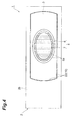
- Fig. 4 is a bottom plan view of the spectral module of Fig. 1
- the rear face (the other surface) 2b of the substrate 2 is provided with a recess 19 adapted to mate with the lens unit 3.
- the recess 19 comprises a bottom face 21 substantially parallel to the rear face 2b of the substrate 2 and a side wall (constituted by first mating sections (side walls opposing each other in the extending direction of grating grooves 6a which will be explained later) and second mating sections (side walls opposing each other in a direction substantially orthogonal to the extending direction of the grating grooves 6a that will be explained later)) 22 and is formed by etching such as to have a predetermined positional relationship with the alignment marks 12a, 12b, 12c, 12d.
- the recess 19 is produced such that the gap formed between the lens unit 3 and the side wall 22 in the longitudinal direction of the substrate 2 is smaller than that formed between the lens unit 3 and the side wall 22 in a direction substantially orthogonal to the longitudinal direction of the substrate 2 (e.g., the gap formed in a direction substantially orthogonal to the longitudinal direction of the substrate 2 is 0 to 100 ⁇ m, while the gap formed in the longitudinal direction of the substrate 2 is 0 to 30 ⁇ m).
- Fig. 5 is a perspective view of the lens unit in the spectral module of Fig. 1 .
- the lens unit 3 is made of the same material as that of the substrate 2, a light transmitting resin, a light transmitting inorganic/organic hybrid material, a light transmitting low melting glass material, a plastic, or the like into such a form (e.g., with a radius of curvature of 6 to 10 mm, a full length in a bottom face 3 a of 12 to 18 mm, a full width in the bottom face 3a (i.e., the distance between side faces 3b) of 6 to 10 mm, and a height of 5 to 8 mm) that a semispherical lens is cut at two planes substantially parallel to each other and substantially orthogonal to the bottom face 3a, so as to form the side faces 3b, and functions as a lens for converging the light L2 spectrally resolved by the spectroscopic unit 4 onto a light detecting unit 5a of
- the lens unit 3 is mated with the recess 19 through an optical resin agent 16. That is, the lens unit 3 is arranged on the rear face 2b side of the substrate 2. Specifically, the lens unit 3 is mated with the recess 19 such that gaps are formed between the lens unit 3 and the side wall 22 of the recess 19, while the optical resin agent 16 is disposed in these gaps and between the bottom face 3a of the lens unit 3 and the bottom face 21 of the recess 19.
- the spectroscopic unit 4 is a reflection type grating having a diffracting layer 6 formed on the outer surface of the lens unit 3 and a reflecting layer 7 formed on the outer surface of the diffracting layer 6.
- the diffracting layer 6 is formed by aligning a plurality of grating grooves 6a in a row longitudinally of the substrate 2, while the extending direction of the grating grooves 6a substantially coincides with a direction substantially orthogonal to the longitudinal direction of the substrate 2.
- the diffracting layer 6 is formed by photocuring a replicating optical resin such as photocurable epoxy, acrylic, and organic/inorganic hybrid resins.
- the reflecting layer 7 is shaped like a film and formed by vapor-depositing Al, Au, or the like on the outer surface of the diffracting layer 6, for example. Regulating the area by which the reflecting layer 7 is formed can adjust the optical NA of the spectral module 1.
- the lens unit 3 and the diffracting layer 6 constituting the spectroscopic unit 4 can also be integrally formed by the materials mentioned above.
- the photodetector 5 is formed into an rectangular plate (e.g., with a full length of 5 to 10 mm, a full width of 1.5 to 3 mm, and a thickness of 0.1 to 0.8 mm).
- the light detecting unit 5a of the photodetector 5 is a CCD image sensor, a PD array, a CMOS image sensor, or the like, in which a plurality of channels are arranged in a row in a direction (i.e., the direction of the row of the grating grooves 6a) substantially orthogonal to the extending direction of the grating grooves 6a of the spectroscopic unit 4.
- the light detecting unit 5a When the light detecting unit 5a is a CCD image sensor, the intensity information of light at its incident position on two-dimensionally arranged pixels is subjected to line binning, so as to yield light intensity information at one-dimensional positions, and the intensity information at the one-dimensional positions is read in time series. That is, a line of pixels subjected to line binning forms one channel.
- the light detecting unit 5a is a PD array or CMOS image sensor
- intensity information of light at its incident position on one-dimensionally arranged pixels is read in time series, whereby one pixel forms one channel.
- the light detecting unit 5a is a PD array or CMOS image sensor in which pixels are arranged two-dimensionally, a line of pixels aligning in a one-dimensional arrangement direction parallel to the extending direction of the grating grooves 6a of the spectroscopic unit 4 forms one channel.
- the light detecting unit 5a is a CCD image sensor, one having a channel interval in the arrangement direction of 12.5 ⁇ m, a channel full length (length of the one-dimensional pixel row subjected to line binning) of 1 mm, and 256 arrangement channels, for example, is used for the photodetector 5.
- the photodetector 5 is also formed with a light transmitting hole 5b, disposed in parallel with the light detecting unit 5a in the channel arrangement direction, for transmitting the light L1 proceeding to the spectroscopic unit 4.
- the light transmitting hole 5b which is a slit (e.g., with a length of 0.5 to 1 mm and a width of 10 to 100 ⁇ m) extending in a direction substantially orthogonal to the longitudinal direction of the substrate 2, is formed by etching or the like while being positioned with respect to the light detecting unit 5a with a high precision.
- a light absorbing layer 13 is formed on the front face 2a of the substrate 2 such as to expose the pad parts 11a, 11b of the wiring pattern 11 and the alignment marks 12a, 12b, 12c, 12d and cover the connection parts 11c of the wiring pattern 11.
- the light absorbing layer 13 is formed with a slit 13a at a position opposing the light transmitting hole 5b of the photodetector 5 so as to transmit the light L1 proceeding to the spectroscopic unit 4 and an opening 13b at a position opposing the light detecting unit 5a so as to transmit the light L2 proceeding to the light detecting unit 5a of the photodetector 5.
- the light absorbing layer 13 is patterned into a predetermined form and integrally shaped by CrO, a multilayer film containing CrO, a black resist, or the like.
- outer terminals of the photodetector 5 are electrically connected to their corresponding pad parts 11a exposed from the light absorbing layer 13.
- the pad parts 11b are electrically connected to external electric elements (not depicted).
- An underfill material 15 which transmits at least the light L2 fills the space on the substrate 2 side of the photodetector 5 (between the photodetector 5 and the substrate 2 or light absorbing layer 13 here), whereby a mechanical strength can be kept.
- the wiring pattern 11 and alignment marks 12a, 12b, 12c, 12d are patterned on the front face 2a of the substrate 2.
- the light absorbing layer 13 is patterned such as to expose the pad parts 11a, 11b and alignment marks 12a, 12b, 12c, 12d and form the slit 13a and opening 13b.
- the light absorbing layer 13 is formed by photolithography so as to be in alignment.
- the recess 19 is formed in the rear face 2b of the substrate 2 by photolithography and etching utilizing a double-sided alignment and exposure system or the like such as to have a predetermined positional relationship with the alignment marks 12a, 12b, 12c, 12d formed in the front face 2a.
- the photodetector 5 is mounted on the light absorbing layer 13 by face-down bonding.
- the photodetector 5 is arranged such that the channel arrangement direction of the light detecting unit 5a substantially coincides with the longitudinal direction of the substrate 2, while the light detecting unit 5a faces the front face 2a of the substrate 2, and mounted at a predetermined position with reference to the alignment marks 12a, 12b, 12c, 12d by image recognition.
- the spectroscopic unit 4 is formed on the lens unit 3.
- a light transmitting master grating (not depicted) inscribed with a grating corresponding to the diffracting layer 6 is brought into contact with a replicating optical resin dropped near the vertex of the lens unit 3.
- the replicating optical resin is hardened by irradiation with light, so as to form the diffracting layer 6 having a plurality of grating grooves 6a extending in a direction substantially orthogonal to the longitudinal direction of the substrate 2.
- the layer is stabilized by heat curing.
- the replicating optical resin is hardened, the master grating is released therefrom, and aluminum or gold is vapor-deposited on the outer face of the diffracting layer 6 through a mask or as a whole, so as to form the reflecting layer 7.
- the photocurable optical resin agent 16 is applied to the recess 19 of the substrate 2. Then, the bottom face 3a side of lens unit 3 is mated with the recess 19. Here, the lens unit 3 is mated therewith such that the extending direction of the grating grooves 6a of the spectroscopic unit 4 substantially coincides with a direction substantially orthogonal to the longitudinal direction of the substrate 2, while the an excess of the resin agent and air is released through the gap between the lens unit 3 and the side wall 22 of the recess 19. Thereafter, the optical resin agent 16 is hardened by irradiation with light, so as to mount the lens unit 3 to the substrate 2.
- this spectral module 1 since the recess 19 has a predetermined positional relationship with the alignment marks 12a, 12b, 12c, 12d for positioning the photodetector 5 with respect to the substrate 2, the spectroscopic unit 4 and the lens unit 3 are positioned with respect to the substrate 2 when the lens unit 3 formed with the spectroscopic unit 4 is simply mated with the recess 19. Also, since the photodetector 5 is positioned with respect to the substrate 2 by the alignment marks 12a, 12b, 12c, 12d in the spectral module 1, positioning the spectroscopic unit 4 with respect to the substrate 2 results in alignment between the spectroscopic unit 4 and the photodetector 5. Therefore, this spectral module 1 achieves so-called passive alignment, which can make it easier to assemble the spectral module.
- the recess 19 is formed such that the gap between the side wall 22 and the lens unit 3 is smaller in a direction substantially coinciding with a direction (i.e., the longitudinal direction of the substrate 2) substantially orthogonal to the extending direction of the grating grooves 6a than in the extending direction of the grating grooves 6a (i.e., a direction substantially orthogonal to the longitudinal direction of the substrate 2).
- this spectral module 1 the alignment between the lens unit 3 and photodetector 5 is effected precisely in a direction substantially orthogonal to the extending direction of the grating grooves 6a, so that the light L2 spectrally resolved by the spectroscopic unit 4 can accurately be made incident on the photodetector 5, whereby the reliability of the spectral module can be improved. Since the channel (pixel line) arrangement direction in the photodetector 5 and the longitudinal direction of the substrate 2 substantially coincide with each other in this spectral module 1, the alignment between the lens unit 3 and photodetector 5 is effected precisely in the channel arrangement direction (i.e., a direction substantially orthogonal to the extending direction of the grating grooves 6a). Hence, in this spectral module 1, the light L2 spectrally resolved by the spectroscopic unit 4 is incident on an appropriate channel without deviating in the channel arrangement direction (channel width direction), whereby the reliability of the spectral module can effectively be improved.
- the gap between the lens unit 3 and side wall 22 is formed greater in the extending direction of the grating grooves 6a, whereby the excess of resin and air can effectively be released through the gap in the extending direction of the grating grooves 6a when bonding the lens unit 3 to the substrate 2 with the optical resin agent. Therefore, this spectral module 1 can suppress unevenness in the optical resin agent 16 and occurrence of bubbles between the lens unit 3 and substrate 2 (i.e., between the lens unit 3 and recess 19), thereby making it possible to mount the lens unit 3 precisely to the substrate 2.
- the present invention is not limited to the above-mentioned first embodiment.
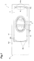
- a recess 33 may comprise an rectangular bottom face 34 substantially parallel to a rear face 32b of a substrate 32 and a side wall 35 substantially perpendicular to the bottom face 34, while the side wall 35 may have mating sections 35a adapted to mate with the lens unit 3 in the longitudinal direction of the substrate 32 and a direction substantially orthogonal to the longitudinal direction and spaced sections 35b deviating from the lens unit 3.
- the excess of resin and air can be released through gaps M formed between the lens unit 3 and the spaced sections 35b, so that the lens unit 3 can be fixed reliably while the resin between the lens unit 3 and bottom face 34 can attain a substantially uniform thickness without causing unevenness in the resin or generating bubbles between the lens unit 3 and substrate 32, whereby the lens unit 3 can be mounted to the substrate 32 with a high horizontal precision.
- a recess 43 may comprise an essentially rectangular bottom face 44 substantially parallel to a rear face 42b of a substrate 42 and a side wall 45 substantially perpendicular to the bottom face 44, while the side wall 45 may have mating sections 45b, which include a part of two pairs of projections 45a projecting to the inside of the recess 43 longitudinally of the substrate 42 and are adapted to mate with the lens unit 3 in the longitudinal direction of the substrate 42 and a direction substantially orthogonal to the longitudinal direction, and spaced sections 45c deviating from the lens unit 3.
- the mating sections 45b include a part of the projections 45a projecting to the inside of the recess 43, gaps N between the lens unit 3 and spaced sections 45c are formed greater than those in the second embodiment, whereby the excess of resin and air can be released effectively when mounting the lens unit 3 to the substrate 42.
- a plurality of spaced sections may be disposed so as to surround the lens unit 3. Since a plurality of gaps are formed between the lens unit 3 and the spaced sections so as to surround the lens unit 3, this structure can efficiently release the excess of resin and air through the plurality of gaps surrounding the lens unit 3 when bonding the lens unit 3 to the substrate with the optical resin agent.
- the recess illustrated in Figs. 6 and 7 may be formed such that the gap between the lens unit 3 and the side face of the recess in a direction substantially coinciding with the longitudinal direction of the substrate is smaller than that in a direction substantially orthogonal to the longitudinal direction of the substrate. This can release the excess of resin and air more effectively.
- the recess may be formed on the substrate by a resin such as a resist or a metal mask instead of etching the substrate.
- the reference unit is not limited to the alignment marks 12a, 12b, 12c, 12d; for example, the recess 19 and photodetector 5 may be positioned with respect to each other while utilizing the wiring pattern 11 as the reference unit. Corner portions in the outer shape of the substrate 2 may also be employed as the reference unit, for example.
- Fig. 8 is a plan view of the second embodiment of the spectral module in accordance with the present invention
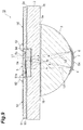
- Fig. 9 is a sectional view taken along the line IX-IX of Fig. 8
- this spectral module 10 comprises a substrate (main unit) 2 for transmitting light L1 incident thereon from the front face (one surface) 2a side, a lens unit (main unit) 3 for transmitting the light L1 incident on the substrate 2, a spectroscopic unit 4 for reflecting and spectrally resolving the light L1 incident on the lens unit 3, and a photodetector 5 for detecting light L2 reflected by the spectroscopic unit 4.
- the substrate 2 is formed into an rectangular plate, while a wiring board 51 shaped like an rectangular plate formed with an opening 51a having an rectangular cross section in which the photodetector 5 is arranged is bonded to the front face 2a of the substrate 2 with a resin agent 53.
- the wiring board 51 is provided with a wiring pattern 52 made of a metal material.
- the wiring pattern 52 has a plurality of pad parts 52a arranged about the opening 51a, a plurality of pad parts 52b arranged at both end portions in the longitudinal direction of the wiring board 51, respectively, and a plurality of connection parts 52c for connecting the corresponding pad parts 52a and 52b to each other.
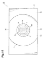
- Fig. 10 is a bottom plan view of the spectral module of Fig. 8 .
- the lens unit 3 is bonded to the rear face (the other surface) 2b of the substrate 2 with an optical resin agent 16 which transmits the light L1, L2 while using outer edge portions of the substrate 2 such as corner portions and side portions thereof as reference units.
- the spectroscopic unit 4 is positioned with respect to the lens unit 3 with a high precision, whereby the outer edge portions of the substrate 2 serve as reference units for positioning the spectroscopic unit 4 with respect to the substrate 2.
- the spectroscopic unit 4 is a reflection type grating having a diffracting layer 6 formed on the outer surface of the lens unit 3, a reflecting layer 7 formed on the outer surface of the diffracting layer 6, and a passivation layer 54 which covers the diffracting layer 6 and reflecting layer 7.
- the diffracting layer 6 is formed by aligning a plurality of grating grooves 6a in a row longitudinally of the substrate 2, while the extending direction of the grating grooves 6a substantially coincides with a direction substantially orthogonal to the longitudinal direction of the substrate 2.
- the photodetector 5 is formed into an rectangular plate, while the surface of the photodetector 5 on the spectroscopic unit 4 side is formed with a light detecting unit 5a.
- the light detecting unit 5a is a CCD image sensor, a PD array, a CMOS image sensor, or the like, in which a plurality of channels are arranged in a row in a direction (i.e., the direction of the row of the grating grooves 6a) substantially orthogonal to the extending direction of the grating grooves 6a of the spectroscopic unit 4.
- the photodetector 5 is also formed with a light transmitting hole 5b, disposed in parallel with the light detecting unit 5a in the channel arrangement direction, for transmitting the light L1 proceeding to the spectroscopic unit 4.
- the light transmitting hole 5b which is a slit extending in a direction substantially orthogonal to the longitudinal direction of the substrate 2, is formed by etching or the like while being positioned with respect to the light detecting unit 5a with a high precision.
- Fig. 11 is an enlarged sectional view of a main part of the spectral module of Fig. 9 .
- the photodetector 5 has a light transmitting plate 56 bonded to the surface of the photodetector 5 on the spectroscopic unit 4 side with an optical resin agent 55, which transmits the light L1, L2, and a light shielding film 57 formed on the surface of the photodetector 5 opposite from the spectroscopic unit 4 in a part opposing the light detecting unit 5a.
- the light transmitting plate 56 covers the light detecting unit 5a and light transmitting hole 5b.
- the light shielding film 57 blocks the light L1 that is going to proceed to the spectroscopic unit 4 without passing through the light transmitting hole 5b or the light L1 that is going to be directly incident on the light detecting unit 5a.
- the wiring board 51 functions to block the light L1 that is going to proceed to the spectroscopic unit 4 without passing through the light transmitting hole 5b.
- a plurality of electrodes 58 are formed on the surface of the photodetector 5 on the spectroscopic unit 4 side, while the surface of the photodetector 5 on the side opposite from the spectroscopic unit 4 is formed with a plurality of terminal electrodes 61 connected to their corresponding electrodes 58 with through-electrodes 59.
- the terminal electrodes 61 are connected to their corresponding pad parts 52a of the wiring board 51 with respective wires 62.
- a light absorbing layer 68 is formed on the surface of the light transmitting plate 56 on the photodetector 5 side.
- the light absorbing layer 68 is formed with a light transmitting hole 68a at a position opposing the light transmitting hole 5b of the photodetector 5 so as to transmit the light L1 proceeding to the spectroscopic unit 4 and a light transmitting hole 68b at a position opposing the light detecting unit 5a of the photodetector 5 so as to transmit the light L2 proceeding to the light detecting unit 5a.
- the light absorbing layer 68 is patterned into a predetermined form and integrally shaped by CrO, a multilayer film containing CrO, a black resist, or the like.
- the light absorbing layer 68 may be formed on the surface of the photodetector 5 on the spectroscopic unit 4 side as illustrated in Fig. 12 .
- the front face 2a of the substrate 2 is provided with a recess 64 having an rectangular cross section adapted to mate with the photodetector 5 through an optical resin agent 63 which transmits the light L1, L2.
- the recess 64 comprises a bottom face 65 substantially parallel to the front face 2a of the substrate 2 and a side wall 66 substantially perpendicular to the bottom face 65 and is formed by etching such as to have a predetermined positional relationship with the outer edge portions of the substrate 2 serving as a reference unit.
- the photodetector 5 projects from the front face 2a of the substrate 2 while mating with the recess 64.
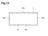
- Fig. 13 is a view illustrating the relationship between the photodetector and recess in the spectral module of Fig. 8 .
- the recess 64 is provided with side walls (third mating sections) 66a adapted to mate with the photodetector 5 in the extending direction of the grating grooves 6a of the spectroscopic unit 4 and side walls (fourth mating sections) 66b adapted to mate with the photodetector 5 in a direction substantially orthogonal to the extending direction of the grating grooves 6a of the spectroscopic unit 4.
- the gap between the photodetector 5 and each side wall 66b is smaller than that between the photodetector 5 and each side wall 66a.
- the spectroscopic unit 4 is formed on the lens unit 3. Specifically, a light transmitting master grating inscribed with a grating corresponding to the diffracting layer 6 is pressed against a replicating optical resin dropped near the vertex of the lens unit 3. Subsequently, in this state, the replicating optical resin is hardened by irradiation with light, preferably followed by heat curing for stabilization, so as to form the diffracting layer 6 having a plurality of grating grooves 6a.
- the master grating is released therefrom, Al, Au, or the like is vapor-deposited on the outer surface of the diffracting layer 6, so as to form the reflecting layer 7, and MgF 2 or the like is vapor-deposited on the outer surface of the diffracting layer 6 and reflecting layer 7, so as to form the passivation layer 54.
- the substrate 2 is prepared and, while employing outer edge portions of the substrate 2 such as corner portions and side portions thereof as reference units, the recess 64 is formed in the front face 2a of the substrate 2 by photolithography and etching utilizing a double-sided alignment and exposure system such as to have a predetermined positional relationship with the reference units.
- the lens unit 3 formed with the spectroscopic unit 4 is bonded to the rear face 2b of the substrate 2 with the optical resin agent 16. Thereafter, the optical resin agent 63 is applied to the recess 64 of the substrate 2, and the photodetector 5 having the light transmitting plate 56 attached thereto is mated with the recess 64. Then, the optical resin agent 63 is hardened by irradiation with light, and the photodetector 5 is mounted to the substrate 2.
- the wiring board 51 is bonded to the front face 2a of the substrate 2 with the resin agent 53. Then, the terminal electrodes 61 of the photodetector 5 and their corresponding pad parts 52a of the wiring board 51 are connected to each other through the wires 62, so as to yield the spectral module 10.
- the photodetector 5 is positioned with respect to the substrate 2 when the photodetector 5 is simply mated with the recess 64.
- the lens unit 3 formed with the spectroscopic unit 4 is positioned with respect to the substrate 2 by the outer edge portions of the substrate 2 serving as reference units, whereby alignment is achieved between the spectroscopic unit 4 and photodetector 5.
- the gap between the side wall 66 of the recess 64 and the photodetector 5 in a direction substantially orthogonal to the extending direction of the grating grooves 6a of the spectroscopic unit 4 is smaller than that in the extending direction of the grating grooves 6a of the spectroscopic unit 4. Therefore, the alignment between the lens unit 3 and photodetector 5 is effected precisely in a direction substantially orthogonal to the extending direction of the grating grooves 6a, so that the light L2 spectrally resolved by the spectroscopic unit 4 can accurately be made incident on the photodetector 5.
- the photodetector 5 has an rectangular form, so as to make the gap between the photodetector 5 and the side wall 66 of the recess 64 longer and the distance to the gap shorter in the extending direction of the grating grooves 6a, whereby the excess of resin and air can be released effectively when bonding the photodetector 5 to the substrate 2 with the optical resin agent 63.
- the spectral module 10 achieves so-called passive alignment, which can make it easy to assemble while keeping reliability.
- the photodetector 5 projects from the front face 2a of the substrate 2 while mating with the recess 64. This can not only make it easier to mate the photodetector 5 with the recess 64 disposed in the front face 2a of the substrate 2, but also reliably press the photodetector 5 against the bottom face 65 of the recess 64, thereby securely releasing the excess of resin and air.
- the photodetector 5 is provided with the light transmitting hole 5b that transmits the light L 1 proceeding to the spectroscopic unit 4. This can achieve passive alignment of the light transmitting hole 5b with respect to the spectroscopic unit 4 and photodetector 5.
- the present invention is not limited to the above-mentioned second embodiment.
- the substrate 2 may be constructed by bonding a plurality of layers of substrates together.
- the substrate 2 is constructed by bonding two layers of substrates 2 1 , 2 2 to each other with the optical resin agent 16 by way of example, the substrate 2 1 arranged on the side opposite from the spectroscopic unit 4 may be provided with an opening having an rectangular cross section, so as to form the recess 64 of the substrate 2.
- a light absorbing layer 67 having a light transmitting hole 67a for transmitting the light L1 proceeding to the spectroscopic unit 4 and a light transmitting hole 67b for transmitting the light L2 proceeding to the light detecting unit 5a of the photodetector 5 may be formed between the substrates 2 1 , 2 2 adjacent to each other or between the substrate 2 2 and lens unit 3. This structure can restrict widening advancing light so as to make it reach a desirable region and effectively inhibit stray light from entering the photodetector 5.
- Examples of the material for the light absorbing layer 67 include black resists, colored resins (e.g., silicone, epoxy, acrylic, urethane, polyimide, and composite resins) containing fillers (such as carbon and oxides), metals such as Cr and Co and oxides thereof, their multilayer films, and porous ceramics and metals or metal oxides.
- the light transmitting holes 67a, 67b in the light absorbing layer 67 may have different sizes, whereby the optical NA can be adjusted.
- a so-called back-illuminated element may be employed as the photodetector 5.
- the electrodes 58 are located on the outer side together with the light detecting unit 5a and thus may be employed as terminal electrodes so as to be connected to the pad parts 52a of the wiring board 51 with the wires 62.
- the substrate 2 and lens unit 3 may be integrally formed by a mold, whereas the lens 3 and diffracting layer 6 may be integrally formed from a light transmitting low melting glass material for shaping a replica or the like.
- the recess 64 may be formed on the front face of the lens unit 3 without using the substrate 2 as a main unit.
- the side wall 66 of the recess 64 adapted to mate with the photodetector 5 may have spaced sections 66c deviating from the photodetector 5.
- Such a structure can release the excess of resin and air more effectively through the gaps between the photodetector 5 and spaced sections 66c when bonding the photodetector 5 to the substrate 2 with the optical resin agent 63. This can suppress unevenness in the resin agent and occurrence of bubbles between the photodetector 5 and substrate 2.
- the present invention may be constructed such that the rear face 2b of the substrate 2 is provided with the recess 19, the lens unit 3 is mated with the recess 19 through the optical resin agent 16, the front face 2a of the substrate 2 is provided with the recess 64, and the photodetector 5 is mated with the recess 64 through the optical resin agent 63.
- the recess 64 serves as a reference unit for positioning the photodetector 5 with respect to the substrate 2
- the recess 19 serves as a reference unit for positioning the spectroscopic unit 4 with respect to the substrate 2.
- the wiring board or light shielding film may be provided therewith.
- the present invention makes it possible to assemble a spectral module easily while keeping the reliability of the spectral module.
Landscapes
- Physics & Mathematics (AREA)
- Spectroscopy & Molecular Physics (AREA)
- General Physics & Mathematics (AREA)
- Optics & Photonics (AREA)
- Engineering & Computer Science (AREA)
- Manufacturing & Machinery (AREA)
- Spectrometry And Color Measurement (AREA)
Abstract
Description
- The present invention relates to a spectral module for spectrally resolving and detecting light.
- As conventional spectral modules, those described in
Patent Literatures 1 to 3 have been known, for example.Patent Literature 1 discloses a spectral module having a block-shaped support which is a biconvex lens, in which one convex surface of the support is provided with a spectroscopic unit such as a diffraction grating, while a photodetector such as a photodiode is disposed on the other convex surface side of the support. -
- Patent Literature 1: Japanese Patent Application Laid-Open No.
4-294223 - Patent Literature 2: Japanese Patent Application Laid-Open No.
2000-65642 - Patent Literature 3: Japanese Patent Application Laid-Open No.
2004-354176 - Meanwhile, when positioning the spectroscopic unit and photodetector and attaching them to the support, the spectral module described in
Patent Literature 1 necessitates so-called active alignment in which, while the light spectrally resolved by the spectroscopic unit is received by the photodetector, the spectroscopic unit is moved relative to the photodetector, and the spectroscopic unit and the photodetector are positioned with respect to each other according to the light-receiving state of the photodetector. However, such active alignment is problematic in that an operation for assembling the spectral module takes a long time. - In view of such circumstances, it is an object of the present invention to provide a spectral module which can be assembled easily while keeping reliability.
- For achieving the above-mentioned object, the spectral module in accordance with the present invention comprises a substrate for transmitting light incident thereon from one surface; a light transmitting unit, disposed on the other surface side of the substrate, for transmitting the light incident on the substrate; a spectroscopic unit, formed with the light transmitting unit, for reflecting and spectrally resolving the light incident on the light transmitting unit; and a photodetector, disposed on the one surface side of the substrate, for detecting the light spectrally resolved by the spectroscopic unit; wherein the other surface is provided with a recess, adapted to mate with the light transmitting unit through an optical resin agent, having a predetermined positional relationship with a reference unit for positioning the photodetector with respect to the substrate; wherein the recess is provided with a first mating section adapted to mate with the light transmitting unit in an extending direction of a grating groove of the spectroscopic unit and a second mating section adapted to mate with the light transmitting unit in a direction substantially orthogonal to the extending direction of the grating groove; and wherein the second mating section and the light transmitting unit have a gap therebetween smaller than that between the first mating section and the light transmitting unit.
- In this spectral module, since the recess has a predetermined positional relationship with the reference unit for positioning the photodetector with respect to the substrate, the spectroscopic unit and the light transmitting unit are positioned with respect to the substrate when the light transmitting unit formed with the spectroscopic unit is simply mated with the recess. Here, the photodetector is positioned with respect to the substrate by the reference unit, whereby alignment is achieved between the spectroscopic unit and the photodetector. In addition, the gap between the mating section and the light transmitting unit in a direction substantially orthogonal to the extending direction of the grating groove of the spectroscopic unit is smaller than that between the mating section and the light transmitting unit in the extending direction of the grating groove of the spectroscopic unit. This achieves the alignment between the light transmitting unit and the photodetector precisely in a direction substantially orthogonal to the extending direction of the grating groove, whereby the light spectrally resolved by the spectroscopic unit can be made accurately incident on the photodetector. When bonding the light transmitting unit to the substrate with the optical resin agent, an excess of resin and air can effectively be released, since the gap between the light transmitting unit and the mating section is formed greater in the extending direction of the grating groove. This spectral module thus achieves so-called passive alignment, which can make it easy to assemble while keeping reliability.
- Preferably, in the spectral module in accordance with the present invention, the recess has a side wall including a spaced section deviating from the first and second mating sections and the light transmitting unit. Such a structure can release the excess of resin and air more effectively through the gap between the light transmitting unit and the spaced section when bonding the light transmitting unit to the substrate with the optical resin agent. This can suppress unevenness in the resin agent and occurrence of bubbles between the light transmitting unit and the substrate, thereby making it possible to mount the light transmitting unit more precisely to the substrate.
- Preferably, the spaced section comprises a plurality of sections disposed so as to surround the light transmitting unit. This structure can release the excess of resin and air through a plurality of gaps more efficiently when bonding the light transmitting unit to the substrate with the optical resin agent.
- In another aspect, the spectral module in accordance with the present invention comprises a substrate for transmitting light incident thereon from one surface; a light transmitting unit, disposed on the other surface side of the substrate, for transmitting the light incident on the substrate; a spectroscopic unit, formed with the light transmitting unit, for reflecting and spectrally resolving the light incident on the light transmitting unit; and a photodetector, disposed on the one surface side of the substrate, for detecting the light spectrally resolved by the spectroscopic unit; wherein the other surface is provided with a recess having a predetermined positional relationship with a reference unit for positioning the photodetector with respect to the substrate; and wherein the light transmitting unit is mated with the recess.
- In this spectral module, since the recess has a predetermined positional relationship with the reference unit for positioning the photodetector with respect to the substrate, the spectroscopic unit and the light transmitting unit are positioned with respect to the substrate when the light transmitting unit formed with the spectroscopic unit is simply mated with the recess. Here, the photodetector is positioned with respect to the substrate by the reference unit, whereby alignment is achieved between the spectroscopic unit and the photodetector. This spectral module thus achieves so-called passive alignment, which can make it easy to assemble while keeping reliability.
- In still another aspect, the spectral module in accordance with the present invention comprises a main unit for transmitting light incident thereon from one surface side; a spectroscopic unit, formed with the main unit, for reflecting and spectrally resolving the light incident on the main unit; and a photodetector, disposed on the one surface side of the main unit, for detecting the light spectrally resolved by the spectroscopic unit; wherein the one surface is provided with a recess, adapted to mate with the photodetector through an optical resin agent, having a predetermined positional relationship with a reference unit for positioning the spectroscopic unit with respect to the main unit; wherein the recess is provided with a third mating section adapted to mate with the photodetector in an extending direction of a grating groove of the spectroscopic unit and a fourth mating section adapted to mate with the photodetector in a direction substantially orthogonal to the extending direction of the grating groove; and wherein the fourth mating section and the photodetector have a gap therebetween smaller than that between the third mating section and the photodetector.
- In this spectral module, since the recess has a predetermined positional relationship with the reference unit for positioning the spectroscopic unit with respect to the main unit, the photodetector is positioned with respect to the main unit when the photodetector is simply mated with the recess. Here, the spectroscopic unit is positioned with respect to the main unit by the reference unit, whereby alignment is achieved between the spectroscopic unit and the photodetector. In addition, the gap between the mating section and the photodetector in a direction substantially orthogonal to the extending direction of the grating groove of the spectroscopic unit is smaller than that between the mating section and the photodetector in the extending direction of the grating groove of the spectroscopic unit. This achieves the alignment between the main unit and the photodetector precisely in a direction substantially orthogonal to the extending direction of the grating groove, whereby the light spectrally resolved by the spectroscopic unit can be made accurately incident on the photodetector. When bonding the photodetector to a substrate with the optical resin agent, an excess of resin and air can effectively be released, since the gap between the photodetector and the mating section is formed greater in the extending direction of the grating groove. This spectral module thus achieves so-called passive alignment, which can make it easy to assemble while keeping reliability.
- Preferably, in the spectral module in accordance with the present invention, the photodetector has an elongated form such as to be longer in a direction substantially orthogonal to the extending direction of the grating groove than in the extending direction of the grating groove. This structure makes the gap between the mating section and the photodetector longer and the distance to the gap shorter in the extending direction of the grating groove than in a direction substantially orthogonal to the extending direction of the grating groove, whereby the excess of resin and air can be moved efficiently to the gap.
- Preferably, in the spectral module in accordance with the present invention, the photodetector projects from the one surface while mating with the recess. This structure can not only make it easier to mate the photodetector with the recess disposed in one surface of the substrate, but also reliably press the photodetector against the bottom face of the recess, thereby securely releasing the excess of resin and air.
- Preferably, in the spectral module in accordance with the present invention, the photodetector is provided with a light transmitting hole for transmitting light proceeding to the spectroscopic unit. This structure can achieve passive alignment of the light transmitting hole with respect to the spectroscopic unit and photodetector.
- The present invention makes it possible to assemble a spectral module easily while keeping the reliability of the spectral module.
-
- [
Fig. 1 ] is a plan view of a first embodiment of the spectral module in accordance with the present invention; - [
Fig. 2 ] is a sectional view taken along the line II-II ofFig. 1 ; - [
Fig. 3 ] is an exploded perspective view of the spectral module ofFig. 1 ; - [
Fig. 4 ] is a bottom plan view of the spectral module ofFig. 1 ; - [
Fig. 5 ] is a perspective view of a lens unit in the spectral module ofFig. 1 ; - [
Fig. 6 ] is a bottom plan view of another embodiment of the spectral module in accordance with the present invention; - [
Fig. 7 ] is a bottom plan view of still another embodiment of the spectral module in accordance with the present invention; - [
Fig. 8 ] is a plan view of a second embodiment of the spectral module in accordance with the present invention; - [
Fig. 9 ] is a sectional view taken along the line IX-IX ofFig. 8 ; - [
Fig. 10 ] is a bottom plan view of the spectral module ofFig. 8 ; - [
Fig. 11 ] is an enlarged sectional view of a main part of the spectral module ofFig. 9 ; - [
Fig. 12 ] is an enlarged sectional view of a main part of still another embodiment of the spectral module in accordance with the present invention; - [
Fig. 13 ] is a view illustrating the relationship between a photodetector and a recess in the spectral module ofFig. 8 ; - [
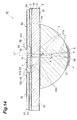
Fig. 14 ] is a sectional view of still another embodiment of the spectral module in accordance with the present invention; and - [
Fig. 15 ] is a view illustrating relationships between the photodetector and recess in other embodiments of the spectral module in accordance with the present invention. - In the following, preferred embodiments of the present invention will be explained in detail with reference to the drawings. In the drawings, the same or equivalent parts will be referred to with the same signs while omitting their overlapping descriptions.
-
Fig. 1 is a plan view of the first embodiment of the spectral module in accordance with the present invention, whileFig. 2 is a sectional view taken along the line II-II ofFig. 1 . As illustrated inFigs. 1 and2 , thisspectral module 1 comprises asubstrate 2 for transmitting light L1 incident thereon from its front face (one surface) 2a, a lens unit (light transmitting unit) 3 for transmitting the light L1 incident on thesubstrate 2, aspectroscopic unit 4 for reflecting and spectrally resolving the light L1 incident on thelens unit 3, and aphotodetector 5 for detecting light L2 reflected by thespectroscopic unit 4. Thespectral module 1 is a microspectral module which spectrally resolves the light L1 into the light L2 corresponding to a plurality of wavelengths with thespectroscopic unit 4 and detects the light L2 with thephotodetector 5, thereby measuring the wavelength distribution, strength of a specific wavelength component, and the like of the light L1. - The
substrate 2 is formed into an rectangular plate (e.g. with a full length of 15 to 20 mm, a full width of 11 to 12 mm, and a thickness of 1 to 3 mm) from any of light transmitting glass materials such as BK7, Pyrex (registered trademark), and silica, plastics, and the like. Formed on thefront face 2a of thesubstrate 2 is awiring pattern 11 made of a monolayer film of Al, Au, or the like or a multilayer film of Cr-Pt-Au, Ti-Pt-Au, Ti-Ni-Au, Cr-Au, or the like. Thewiring pattern 11 has a plurality ofpad parts 11 a arranged at the center portion of thesubstrate 2, a plurality ofpad parts 11b arranged at one end portion in the longitudinal direction of thesubstrate 2, and a plurality ofconnection parts 11c for connecting thecorresponding pad parts wiring pattern 11 also has an reflectinglayerantireflecting layer 11d made of a monolayer film of CrO or the like or a multilayer film of Cr-CrO or the like on thefront face 2a side of thesubstrate 2. - Further, cross-shaped alignment marks (reference units) 12a, 12b, 12c, 12d for positioning the
photodetector 5 with respect to thesubstrate 2 are formed in thefront face 2a of thesubstrate 2 by a structure similar to that of thewiring pattern 11. The alignment marks 12a, 12b are formed at both end portions in the longitudinal direction of thesubstrate 2, respectively, each arranged at the center position in a direction substantially orthogonal to the longitudinal direction of thesubstrate 2. The alignment marks 12c, 12d are formed at both end portions in a direction substantially orthogonal to the longitudinal direction of thesubstrate 2, respectively, each arranged at the center position in the longitudinal direction of thesubstrate 2. -
Fig. 3 is an exploded perspective view of the spectral module ofFig. 1 , whileFig. 4 is a bottom plan view of the spectral module ofFig. 1 . As illustrated inFigs. 3 and4 , the rear face (the other surface) 2b of thesubstrate 2 is provided with arecess 19 adapted to mate with thelens unit 3. Therecess 19 comprises abottom face 21 substantially parallel to therear face 2b of thesubstrate 2 and a side wall (constituted by first mating sections (side walls opposing each other in the extending direction of gratinggrooves 6a which will be explained later) and second mating sections (side walls opposing each other in a direction substantially orthogonal to the extending direction of thegrating grooves 6a that will be explained later)) 22 and is formed by etching such as to have a predetermined positional relationship with the alignment marks 12a, 12b, 12c, 12d. Therecess 19 is produced such that the gap formed between thelens unit 3 and theside wall 22 in the longitudinal direction of thesubstrate 2 is smaller than that formed between thelens unit 3 and theside wall 22 in a direction substantially orthogonal to the longitudinal direction of the substrate 2 (e.g., the gap formed in a direction substantially orthogonal to the longitudinal direction of thesubstrate 2 is 0 to 100 µm, while the gap formed in the longitudinal direction of thesubstrate 2 is 0 to 30 µm). -
Fig. 5 is a perspective view of the lens unit in the spectral module ofFig. 1 . As illustrated inFig. 5 , thelens unit 3 is made of the same material as that of thesubstrate 2, a light transmitting resin, a light transmitting inorganic/organic hybrid material, a light transmitting low melting glass material, a plastic, or the like into such a form (e.g., with a radius of curvature of 6 to 10 mm, a full length in abottom face 3 a of 12 to 18 mm, a full width in thebottom face 3a (i.e., the distance between side faces 3b) of 6 to 10 mm, and a height of 5 to 8 mm) that a semispherical lens is cut at two planes substantially parallel to each other and substantially orthogonal to thebottom face 3a, so as to form the side faces 3b, and functions as a lens for converging the light L2 spectrally resolved by thespectroscopic unit 4 onto alight detecting unit 5a of thephotodetector 5. The lens form is not limited to a spherical lens, but may be an aspherical lens as well. - As illustrated in
Figs. 2 and3 , thelens unit 3 is mated with therecess 19 through anoptical resin agent 16. That is, thelens unit 3 is arranged on therear face 2b side of thesubstrate 2. Specifically, thelens unit 3 is mated with therecess 19 such that gaps are formed between thelens unit 3 and theside wall 22 of therecess 19, while theoptical resin agent 16 is disposed in these gaps and between thebottom face 3a of thelens unit 3 and thebottom face 21 of therecess 19. - As illustrated in
Figs. 2 to 4 , thespectroscopic unit 4 is a reflection type grating having a diffractinglayer 6 formed on the outer surface of thelens unit 3 and a reflectinglayer 7 formed on the outer surface of the diffractinglayer 6. The diffractinglayer 6 is formed by aligning a plurality ofgrating grooves 6a in a row longitudinally of thesubstrate 2, while the extending direction of thegrating grooves 6a substantially coincides with a direction substantially orthogonal to the longitudinal direction of thesubstrate 2. While employing a blazed grating having a sawtooth cross section, a binary grating having a rectangular cross section, a holographic grating having a sinusoidal cross section, or the like, for example, the diffractinglayer 6 is formed by photocuring a replicating optical resin such as photocurable epoxy, acrylic, and organic/inorganic hybrid resins. The reflectinglayer 7 is shaped like a film and formed by vapor-depositing Al, Au, or the like on the outer surface of the diffractinglayer 6, for example. Regulating the area by which the reflectinglayer 7 is formed can adjust the optical NA of thespectral module 1. Thelens unit 3 and the diffractinglayer 6 constituting thespectroscopic unit 4 can also be integrally formed by the materials mentioned above. - As illustrated in
Figs. 1 and2 , thephotodetector 5 is formed into an rectangular plate (e.g., with a full length of 5 to 10 mm, a full width of 1.5 to 3 mm, and a thickness of 0.1 to 0.8 mm). Thelight detecting unit 5a of thephotodetector 5 is a CCD image sensor, a PD array, a CMOS image sensor, or the like, in which a plurality of channels are arranged in a row in a direction (i.e., the direction of the row of thegrating grooves 6a) substantially orthogonal to the extending direction of thegrating grooves 6a of thespectroscopic unit 4. - When the
light detecting unit 5a is a CCD image sensor, the intensity information of light at its incident position on two-dimensionally arranged pixels is subjected to line binning, so as to yield light intensity information at one-dimensional positions, and the intensity information at the one-dimensional positions is read in time series. That is, a line of pixels subjected to line binning forms one channel. In the case where thelight detecting unit 5a is a PD array or CMOS image sensor, intensity information of light at its incident position on one-dimensionally arranged pixels is read in time series, whereby one pixel forms one channel. - When the
light detecting unit 5a is a PD array or CMOS image sensor in which pixels are arranged two-dimensionally, a line of pixels aligning in a one-dimensional arrangement direction parallel to the extending direction of thegrating grooves 6a of thespectroscopic unit 4 forms one channel. When thelight detecting unit 5a is a CCD image sensor, one having a channel interval in the arrangement direction of 12.5 µm, a channel full length (length of the one-dimensional pixel row subjected to line binning) of 1 mm, and 256 arrangement channels, for example, is used for thephotodetector 5. - The
photodetector 5 is also formed with alight transmitting hole 5b, disposed in parallel with thelight detecting unit 5a in the channel arrangement direction, for transmitting the light L1 proceeding to thespectroscopic unit 4. Thelight transmitting hole 5b, which is a slit (e.g., with a length of 0.5 to 1 mm and a width of 10 to 100 µm) extending in a direction substantially orthogonal to the longitudinal direction of thesubstrate 2, is formed by etching or the like while being positioned with respect to thelight detecting unit 5a with a high precision. - Also, a
light absorbing layer 13 is formed on thefront face 2a of thesubstrate 2 such as to expose thepad parts wiring pattern 11 and the alignment marks 12a, 12b, 12c, 12d and cover theconnection parts 11c of thewiring pattern 11. Thelight absorbing layer 13 is formed with aslit 13a at a position opposing thelight transmitting hole 5b of thephotodetector 5 so as to transmit the light L1 proceeding to thespectroscopic unit 4 and anopening 13b at a position opposing thelight detecting unit 5a so as to transmit the light L2 proceeding to thelight detecting unit 5a of thephotodetector 5. Thelight absorbing layer 13 is patterned into a predetermined form and integrally shaped by CrO, a multilayer film containing CrO, a black resist, or the like. - By face-down bonding through
bumps 14, outer terminals of thephotodetector 5 are electrically connected to theircorresponding pad parts 11a exposed from thelight absorbing layer 13. Thepad parts 11b are electrically connected to external electric elements (not depicted). Anunderfill material 15 which transmits at least the light L2 fills the space on thesubstrate 2 side of the photodetector 5 (between thephotodetector 5 and thesubstrate 2 or light absorbinglayer 13 here), whereby a mechanical strength can be kept. - A method of manufacturing the above-mentioned
spectral module 1 will now be explained. - First, the
wiring pattern 11 andalignment marks front face 2a of thesubstrate 2. Thereafter, thelight absorbing layer 13 is patterned such as to expose thepad parts alignment marks slit 13a andopening 13b. Thelight absorbing layer 13 is formed by photolithography so as to be in alignment. Therecess 19 is formed in therear face 2b of thesubstrate 2 by photolithography and etching utilizing a double-sided alignment and exposure system or the like such as to have a predetermined positional relationship with the alignment marks 12a, 12b, 12c, 12d formed in thefront face 2a. - The
photodetector 5 is mounted on thelight absorbing layer 13 by face-down bonding. Here, thephotodetector 5 is arranged such that the channel arrangement direction of thelight detecting unit 5a substantially coincides with the longitudinal direction of thesubstrate 2, while thelight detecting unit 5a faces thefront face 2a of thesubstrate 2, and mounted at a predetermined position with reference to the alignment marks 12a, 12b, 12c, 12d by image recognition. - On the other hand, the
spectroscopic unit 4 is formed on thelens unit 3. First, a light transmitting master grating (not depicted) inscribed with a grating corresponding to the diffractinglayer 6 is brought into contact with a replicating optical resin dropped near the vertex of thelens unit 3. Subsequently, while in contact with the master grating, the replicating optical resin is hardened by irradiation with light, so as to form the diffractinglayer 6 having a plurality ofgrating grooves 6a extending in a direction substantially orthogonal to the longitudinal direction of thesubstrate 2. Preferably, after being hardened, the layer is stabilized by heat curing. When the replicating optical resin is hardened, the master grating is released therefrom, and aluminum or gold is vapor-deposited on the outer face of the diffractinglayer 6 through a mask or as a whole, so as to form the reflectinglayer 7. - Next, the photocurable
optical resin agent 16 is applied to therecess 19 of thesubstrate 2. Then, thebottom face 3a side oflens unit 3 is mated with therecess 19. Here, thelens unit 3 is mated therewith such that the extending direction of thegrating grooves 6a of thespectroscopic unit 4 substantially coincides with a direction substantially orthogonal to the longitudinal direction of thesubstrate 2, while the an excess of the resin agent and air is released through the gap between thelens unit 3 and theside wall 22 of therecess 19. Thereafter, theoptical resin agent 16 is hardened by irradiation with light, so as to mount thelens unit 3 to thesubstrate 2. - Operations and effects of the above-mentioned
spectral module 1 will now be explained. - In this
spectral module 1, since therecess 19 has a predetermined positional relationship with the alignment marks 12a, 12b, 12c, 12d for positioning thephotodetector 5 with respect to thesubstrate 2, thespectroscopic unit 4 and thelens unit 3 are positioned with respect to thesubstrate 2 when thelens unit 3 formed with thespectroscopic unit 4 is simply mated with therecess 19. Also, since thephotodetector 5 is positioned with respect to thesubstrate 2 by the alignment marks 12a, 12b, 12c, 12d in thespectral module 1, positioning thespectroscopic unit 4 with respect to thesubstrate 2 results in alignment between thespectroscopic unit 4 and thephotodetector 5. Therefore, thisspectral module 1 achieves so-called passive alignment, which can make it easier to assemble the spectral module. - In this
spectral module 1, therecess 19 is formed such that the gap between theside wall 22 and thelens unit 3 is smaller in a direction substantially coinciding with a direction (i.e., the longitudinal direction of the substrate 2) substantially orthogonal to the extending direction of thegrating grooves 6a than in the extending direction of thegrating grooves 6a (i.e., a direction substantially orthogonal to the longitudinal direction of the substrate 2). Therefore, in thisspectral module 1, the alignment between thelens unit 3 andphotodetector 5 is effected precisely in a direction substantially orthogonal to the extending direction of thegrating grooves 6a, so that the light L2 spectrally resolved by thespectroscopic unit 4 can accurately be made incident on thephotodetector 5, whereby the reliability of the spectral module can be improved. Since the channel (pixel line) arrangement direction in thephotodetector 5 and the longitudinal direction of thesubstrate 2 substantially coincide with each other in thisspectral module 1, the alignment between thelens unit 3 andphotodetector 5 is effected precisely in the channel arrangement direction (i.e., a direction substantially orthogonal to the extending direction of thegrating grooves 6a). Hence, in thisspectral module 1, the light L2 spectrally resolved by thespectroscopic unit 4 is incident on an appropriate channel without deviating in the channel arrangement direction (channel width direction), whereby the reliability of the spectral module can effectively be improved. - Also, in the
spectral module 1, the gap between thelens unit 3 andside wall 22 is formed greater in the extending direction of thegrating grooves 6a, whereby the excess of resin and air can effectively be released through the gap in the extending direction of thegrating grooves 6a when bonding thelens unit 3 to thesubstrate 2 with the optical resin agent. Therefore, thisspectral module 1 can suppress unevenness in theoptical resin agent 16 and occurrence of bubbles between thelens unit 3 and substrate 2 (i.e., between thelens unit 3 and recess 19), thereby making it possible to mount thelens unit 3 precisely to thesubstrate 2. - The present invention is not limited to the above-mentioned first embodiment.
- For example, as illustrated in
Fig. 6 , arecess 33 may comprise an rectangular bottom face 34 substantially parallel to arear face 32b of asubstrate 32 and a side wall 35 substantially perpendicular to thebottom face 34, while the side wall 35 may havemating sections 35a adapted to mate with thelens unit 3 in the longitudinal direction of thesubstrate 32 and a direction substantially orthogonal to the longitudinal direction and spacedsections 35b deviating from thelens unit 3. In this case, when mounting thelens unit 3 to thesubstrate 32, the excess of resin and air can be released through gaps M formed between thelens unit 3 and the spacedsections 35b, so that thelens unit 3 can be fixed reliably while the resin between thelens unit 3 andbottom face 34 can attain a substantially uniform thickness without causing unevenness in the resin or generating bubbles between thelens unit 3 andsubstrate 32, whereby thelens unit 3 can be mounted to thesubstrate 32 with a high horizontal precision. - As illustrated in
Fig. 7 , arecess 43 may comprise an essentially rectangularbottom face 44 substantially parallel to arear face 42b of asubstrate 42 and a side wall 45 substantially perpendicular to thebottom face 44, while the side wall 45 may havemating sections 45b, which include a part of two pairs ofprojections 45a projecting to the inside of therecess 43 longitudinally of thesubstrate 42 and are adapted to mate with thelens unit 3 in the longitudinal direction of thesubstrate 42 and a direction substantially orthogonal to the longitudinal direction, and spacedsections 45c deviating from thelens unit 3. In this case, since themating sections 45b include a part of theprojections 45a projecting to the inside of therecess 43, gaps N between thelens unit 3 and spacedsections 45c are formed greater than those in the second embodiment, whereby the excess of resin and air can be released effectively when mounting thelens unit 3 to thesubstrate 42. - As illustrated in
Figs. 6 and7 , a plurality of spaced sections may be disposed so as to surround thelens unit 3. Since a plurality of gaps are formed between thelens unit 3 and the spaced sections so as to surround thelens unit 3, this structure can efficiently release the excess of resin and air through the plurality of gaps surrounding thelens unit 3 when bonding thelens unit 3 to the substrate with the optical resin agent. - The recess illustrated in
Figs. 6 and7 may be formed such that the gap between thelens unit 3 and the side face of the recess in a direction substantially coinciding with the longitudinal direction of the substrate is smaller than that in a direction substantially orthogonal to the longitudinal direction of the substrate. This can release the excess of resin and air more effectively. - The recess may be formed on the substrate by a resin such as a resist or a metal mask instead of etching the substrate.
- The reference unit is not limited to the alignment marks 12a, 12b, 12c, 12d; for example, the
recess 19 andphotodetector 5 may be positioned with respect to each other while utilizing thewiring pattern 11 as the reference unit. Corner portions in the outer shape of thesubstrate 2 may also be employed as the reference unit, for example. -
Fig. 8 is a plan view of the second embodiment of the spectral module in accordance with the present invention, whileFig. 9 is a sectional view taken along the line IX-IX ofFig. 8 . As illustrated inFigs. 8 and9 , thisspectral module 10 comprises a substrate (main unit) 2 for transmitting light L1 incident thereon from the front face (one surface) 2a side, a lens unit (main unit) 3 for transmitting the light L1 incident on thesubstrate 2, aspectroscopic unit 4 for reflecting and spectrally resolving the light L1 incident on thelens unit 3, and aphotodetector 5 for detecting light L2 reflected by thespectroscopic unit 4. - The
substrate 2 is formed into an rectangular plate, while awiring board 51 shaped like an rectangular plate formed with anopening 51a having an rectangular cross section in which thephotodetector 5 is arranged is bonded to thefront face 2a of thesubstrate 2 with aresin agent 53. Thewiring board 51 is provided with awiring pattern 52 made of a metal material. Thewiring pattern 52 has a plurality ofpad parts 52a arranged about theopening 51a, a plurality ofpad parts 52b arranged at both end portions in the longitudinal direction of thewiring board 51, respectively, and a plurality ofconnection parts 52c for connecting thecorresponding pad parts -
Fig. 10 is a bottom plan view of the spectral module ofFig. 8 . As illustrated inFigs. 9 and10 , thelens unit 3 is bonded to the rear face (the other surface) 2b of thesubstrate 2 with anoptical resin agent 16 which transmits the light L1, L2 while using outer edge portions of thesubstrate 2 such as corner portions and side portions thereof as reference units. Here, thespectroscopic unit 4 is positioned with respect to thelens unit 3 with a high precision, whereby the outer edge portions of thesubstrate 2 serve as reference units for positioning thespectroscopic unit 4 with respect to thesubstrate 2. - The
spectroscopic unit 4 is a reflection type grating having a diffractinglayer 6 formed on the outer surface of thelens unit 3, a reflectinglayer 7 formed on the outer surface of the diffractinglayer 6, and apassivation layer 54 which covers the diffractinglayer 6 and reflectinglayer 7. The diffractinglayer 6 is formed by aligning a plurality ofgrating grooves 6a in a row longitudinally of thesubstrate 2, while the extending direction of thegrating grooves 6a substantially coincides with a direction substantially orthogonal to the longitudinal direction of thesubstrate 2. - As illustrated in
Figs. 8 and9 , thephotodetector 5 is formed into an rectangular plate, while the surface of thephotodetector 5 on thespectroscopic unit 4 side is formed with alight detecting unit 5a. Thelight detecting unit 5a is a CCD image sensor, a PD array, a CMOS image sensor, or the like, in which a plurality of channels are arranged in a row in a direction (i.e., the direction of the row of thegrating grooves 6a) substantially orthogonal to the extending direction of thegrating grooves 6a of thespectroscopic unit 4. - The
photodetector 5 is also formed with alight transmitting hole 5b, disposed in parallel with thelight detecting unit 5a in the channel arrangement direction, for transmitting the light L1 proceeding to thespectroscopic unit 4. Thelight transmitting hole 5b, which is a slit extending in a direction substantially orthogonal to the longitudinal direction of thesubstrate 2, is formed by etching or the like while being positioned with respect to thelight detecting unit 5a with a high precision. -
Fig. 11 is an enlarged sectional view of a main part of the spectral module ofFig. 9 . As illustrated inFig. 11 , thephotodetector 5 has alight transmitting plate 56 bonded to the surface of thephotodetector 5 on thespectroscopic unit 4 side with anoptical resin agent 55, which transmits the light L1, L2, and alight shielding film 57 formed on the surface of thephotodetector 5 opposite from thespectroscopic unit 4 in a part opposing thelight detecting unit 5a. Thelight transmitting plate 56 covers thelight detecting unit 5a andlight transmitting hole 5b. Thelight shielding film 57 blocks the light L1 that is going to proceed to thespectroscopic unit 4 without passing through thelight transmitting hole 5b or the light L1 that is going to be directly incident on thelight detecting unit 5a. As with thelight shielding film 57, thewiring board 51 functions to block the light L1 that is going to proceed to thespectroscopic unit 4 without passing through thelight transmitting hole 5b. - A plurality of
electrodes 58 are formed on the surface of thephotodetector 5 on thespectroscopic unit 4 side, while the surface of thephotodetector 5 on the side opposite from thespectroscopic unit 4 is formed with a plurality ofterminal electrodes 61 connected to theircorresponding electrodes 58 with through-electrodes 59. Theterminal electrodes 61 are connected to theircorresponding pad parts 52a of thewiring board 51 withrespective wires 62. Hence, electric signals generated in thelight detecting unit 5a are taken out through theelectrodes 58, through-electrodes 59,terminal electrodes 61,pad parts 52a,connection parts 52c, and padparts 52b. - A
light absorbing layer 68 is formed on the surface of thelight transmitting plate 56 on thephotodetector 5 side. Thelight absorbing layer 68 is formed with alight transmitting hole 68a at a position opposing thelight transmitting hole 5b of thephotodetector 5 so as to transmit the light L1 proceeding to thespectroscopic unit 4 and alight transmitting hole 68b at a position opposing thelight detecting unit 5a of thephotodetector 5 so as to transmit the light L2 proceeding to thelight detecting unit 5a. Thelight absorbing layer 68 is patterned into a predetermined form and integrally shaped by CrO, a multilayer film containing CrO, a black resist, or the like. Thelight absorbing layer 68 may be formed on the surface of thephotodetector 5 on thespectroscopic unit 4 side as illustrated inFig. 12 . - As illustrated in
Fig. 11 , thefront face 2a of thesubstrate 2 is provided with arecess 64 having an rectangular cross section adapted to mate with thephotodetector 5 through anoptical resin agent 63 which transmits the light L1, L2. Therecess 64 comprises abottom face 65 substantially parallel to thefront face 2a of thesubstrate 2 and aside wall 66 substantially perpendicular to thebottom face 65 and is formed by etching such as to have a predetermined positional relationship with the outer edge portions of thesubstrate 2 serving as a reference unit. Thephotodetector 5 projects from thefront face 2a of thesubstrate 2 while mating with therecess 64. -
Fig. 13 is a view illustrating the relationship between the photodetector and recess in the spectral module ofFig. 8 . As illustrated inFig. 13 , therecess 64 is provided with side walls (third mating sections) 66a adapted to mate with thephotodetector 5 in the extending direction of thegrating grooves 6a of thespectroscopic unit 4 and side walls (fourth mating sections) 66b adapted to mate with thephotodetector 5 in a direction substantially orthogonal to the extending direction of thegrating grooves 6a of thespectroscopic unit 4. The gap between thephotodetector 5 and eachside wall 66b is smaller than that between thephotodetector 5 and eachside wall 66a. - A method of manufacturing the above-mentioned
spectral module 10 will be explained. - First, the
spectroscopic unit 4 is formed on thelens unit 3. Specifically, a light transmitting master grating inscribed with a grating corresponding to the diffractinglayer 6 is pressed against a replicating optical resin dropped near the vertex of thelens unit 3. Subsequently, in this state, the replicating optical resin is hardened by irradiation with light, preferably followed by heat curing for stabilization, so as to form the diffractinglayer 6 having a plurality ofgrating grooves 6a. Thereafter, the master grating is released therefrom, Al, Au, or the like is vapor-deposited on the outer surface of the diffractinglayer 6, so as to form the reflectinglayer 7, and MgF2 or the like is vapor-deposited on the outer surface of the diffractinglayer 6 and reflectinglayer 7, so as to form thepassivation layer 54. - On the other hand, the
substrate 2 is prepared and, while employing outer edge portions of thesubstrate 2 such as corner portions and side portions thereof as reference units, therecess 64 is formed in thefront face 2a of thesubstrate 2 by photolithography and etching utilizing a double-sided alignment and exposure system such as to have a predetermined positional relationship with the reference units. - While using outer edge portions of the
substrate 2 such as corner portions and side portions thereof as reference units, thelens unit 3 formed with thespectroscopic unit 4 is bonded to therear face 2b of thesubstrate 2 with theoptical resin agent 16. Thereafter, theoptical resin agent 63 is applied to therecess 64 of thesubstrate 2, and thephotodetector 5 having thelight transmitting plate 56 attached thereto is mated with therecess 64. Then, theoptical resin agent 63 is hardened by irradiation with light, and thephotodetector 5 is mounted to thesubstrate 2. - Subsequently, the
wiring board 51 is bonded to thefront face 2a of thesubstrate 2 with theresin agent 53. Then, theterminal electrodes 61 of thephotodetector 5 and theircorresponding pad parts 52a of thewiring board 51 are connected to each other through thewires 62, so as to yield thespectral module 10. - As explained in the foregoing, since the
recess 64 has a predetermined positional relationship with the outer edge portions of thesubstrate 2 serving as reference units for positioning thespectroscopic unit 4 with respect to thesubstrate 2 in thespectral module 10, thephotodetector 5 is positioned with respect to thesubstrate 2 when thephotodetector 5 is simply mated with therecess 64. Here, thelens unit 3 formed with thespectroscopic unit 4 is positioned with respect to thesubstrate 2 by the outer edge portions of thesubstrate 2 serving as reference units, whereby alignment is achieved between thespectroscopic unit 4 andphotodetector 5. Also, the gap between theside wall 66 of therecess 64 and thephotodetector 5 in a direction substantially orthogonal to the extending direction of thegrating grooves 6a of thespectroscopic unit 4 is smaller than that in the extending direction of thegrating grooves 6a of thespectroscopic unit 4. Therefore, the alignment between thelens unit 3 andphotodetector 5 is effected precisely in a direction substantially orthogonal to the extending direction of thegrating grooves 6a, so that the light L2 spectrally resolved by thespectroscopic unit 4 can accurately be made incident on thephotodetector 5. Further, thephotodetector 5 has an rectangular form, so as to make the gap between thephotodetector 5 and theside wall 66 of therecess 64 longer and the distance to the gap shorter in the extending direction of thegrating grooves 6a, whereby the excess of resin and air can be released effectively when bonding thephotodetector 5 to thesubstrate 2 with theoptical resin agent 63. Thus, thespectral module 10 achieves so-called passive alignment, which can make it easy to assemble while keeping reliability. - In the
spectral module 10, thephotodetector 5 projects from thefront face 2a of thesubstrate 2 while mating with therecess 64. This can not only make it easier to mate thephotodetector 5 with therecess 64 disposed in thefront face 2a of thesubstrate 2, but also reliably press thephotodetector 5 against thebottom face 65 of therecess 64, thereby securely releasing the excess of resin and air. - In the
spectral module 10, thephotodetector 5 is provided with thelight transmitting hole 5b that transmits thelight L 1 proceeding to thespectroscopic unit 4. This can achieve passive alignment of thelight transmitting hole 5b with respect to thespectroscopic unit 4 andphotodetector 5. - The present invention is not limited to the above-mentioned second embodiment.
- For example, as illustrated in
Fig. 14 , thesubstrate 2 may be constructed by bonding a plurality of layers of substrates together. When thesubstrate 2 is constructed by bonding two layers ofsubstrates optical resin agent 16 by way of example, thesubstrate 21 arranged on the side opposite from thespectroscopic unit 4 may be provided with an opening having an rectangular cross section, so as to form therecess 64 of thesubstrate 2. - A
light absorbing layer 67 having alight transmitting hole 67a for transmitting the light L1 proceeding to thespectroscopic unit 4 and alight transmitting hole 67b for transmitting the light L2 proceeding to thelight detecting unit 5a of thephotodetector 5 may be formed between thesubstrates substrate 22 andlens unit 3. This structure can restrict widening advancing light so as to make it reach a desirable region and effectively inhibit stray light from entering thephotodetector 5. - Examples of the material for the
light absorbing layer 67 include black resists, colored resins (e.g., silicone, epoxy, acrylic, urethane, polyimide, and composite resins) containing fillers (such as carbon and oxides), metals such as Cr and Co and oxides thereof, their multilayer films, and porous ceramics and metals or metal oxides. Thelight transmitting holes light absorbing layer 67 may have different sizes, whereby the optical NA can be adjusted. - As illustrated in
Fig. 14 , a so-called back-illuminated element may be employed as thephotodetector 5. In this case, theelectrodes 58 are located on the outer side together with thelight detecting unit 5a and thus may be employed as terminal electrodes so as to be connected to thepad parts 52a of thewiring board 51 with thewires 62. Thesubstrate 2 andlens unit 3 may be integrally formed by a mold, whereas thelens 3 and diffractinglayer 6 may be integrally formed from a light transmitting low melting glass material for shaping a replica or the like. Therecess 64 may be formed on the front face of thelens unit 3 without using thesubstrate 2 as a main unit. - As illustrated in
Fig. 15 , theside wall 66 of therecess 64 adapted to mate with thephotodetector 5 may have spacedsections 66c deviating from thephotodetector 5. Such a structure can release the excess of resin and air more effectively through the gaps between thephotodetector 5 and spacedsections 66c when bonding thephotodetector 5 to thesubstrate 2 with theoptical resin agent 63. This can suppress unevenness in the resin agent and occurrence of bubbles between thephotodetector 5 andsubstrate 2. - Without being limited to the above-mentioned first and second embodiments, the present invention may be constructed such that the
rear face 2b of thesubstrate 2 is provided with therecess 19, thelens unit 3 is mated with therecess 19 through theoptical resin agent 16, thefront face 2a of thesubstrate 2 is provided with therecess 64, and thephotodetector 5 is mated with therecess 64 through theoptical resin agent 63. In this case, by way of example, therecess 64 serves as a reference unit for positioning thephotodetector 5 with respect to thesubstrate 2, while therecess 19 serves as a reference unit for positioning thespectroscopic unit 4 with respect to thesubstrate 2. Instead of forming thephotodetector 5 with thelight transmitting hole 5b for transmitting the light L1 proceeding to thespectroscopic unit 4, the wiring board or light shielding film may be provided therewith. - The present invention makes it possible to assemble a spectral module easily while keeping the reliability of the spectral module.
- 1, 10... spectral module; 2... substrate (main unit); 2a... front face (one surface); 2b...rear face (the other surface); 3...lens unit (light transmitting unit or main unit); 4... spectroscopic unit; 5... photodetector; 6a... grating groove; 16... optical resin agent; 19...recess; 22...side wall (first and second mating sections); 63...optical resin agent; 64...recess; 66a...side wall (third mating section); 66b...side wall (fourth mating section)
Claims (8)
- A spectral module comprising:a substrate for transmitting light incident thereon from one surface;a light transmitting unit, disposed on the other surface side of the substrate, for transmitting the light incident on the substrate;a spectroscopic unit, formed with the light transmitting unit, for reflecting and spectrally resolving the light incident on the light transmitting unit; anda photodetector, disposed on the one surface side of the substrate, for detecting the light spectrally resolved by the spectroscopic unit;wherein the other surface is provided with a recess, adapted to mate with the light transmitting unit through an optical resin agent, having a predetermined positional relationship with a reference unit for positioning the photodetector with respect to the substrate;wherein the recess is provided with a first mating section adapted to mate with the light transmitting unit in an extending direction of a grating groove of the spectroscopic unit and a second mating section adapted to mate with the light transmitting unit in a direction substantially orthogonal to the extending direction of the grating groove; andwherein the second mating section and the light transmitting unit have a gap therebetween smaller than that between the first mating section and the light transmitting unit.
- A spectral module according to claim 1, wherein a side wall of the recess includes a spaced section deviating from the first and second mating sections and the light transmitting unit.
- A spectral module according to claim 2, wherein the spaced section comprises a plurality of sections disposed so as to surround the light transmitting unit.
- A spectral module comprising:a substrate for transmitting light incident thereon from one surface;a light transmitting unit, disposed on the other surface side of the substrate, for transmitting the light incident on the substrate;a spectroscopic unit, formed with the light transmitting unit, for reflecting and spectrally resolving the light incident on the light transmitting unit; anda photodetector, disposed on the one surface side of the substrate, for detecting the light spectrally resolved by the spectroscopic unit;wherein the other surface is provided with a recess having a predetermined positional relationship with a reference unit for positioning the photodetector with respect to the substrate; andwherein the light transmitting unit is mated with the recess.
- A spectral module comprising:a main unit for transmitting light incident thereon from one surface side;a spectroscopic unit, formed with the main unit, for reflecting and spectrally resolving the light incident on the main unit; anda photodetector, disposed on the one surface side of the main unit, for detecting the light spectrally resolved by the spectroscopic unit;wherein the one surface is provided with a recess, adapted to mate with the photodetector through an optical resin agent, having a predetermined positional relationship with a reference unit for positioning the spectroscopic unit with respect to the main unit;wherein the recess is provided with a third mating section adapted to mate with the photodetector in an extending direction of a grating groove of the spectroscopic unit and a fourth mating section adapted to mate with the photodetector in a direction substantially orthogonal to the extending direction of the grating groove; andwherein the fourth mating section and the photodetector have a gap therebetween smaller than that between the third mating section and the photodetector.
- A spectral module according to claim 5, wherein the photodetector has an elongated form such as to be longer in a direction substantially orthogonal to the extending direction of the grating groove than in the extending direction of the grating groove.
- A spectral module according to claim 5, wherein the photodetector projects from the one surface while mating with the recess.
- A spectral module according to claim 5, wherein the photodetector is provided with a light transmitting hole for transmitting light proceeding to the spectroscopic unit.
Applications Claiming Priority (3)
| Application Number | Priority Date | Filing Date | Title |
|---|---|---|---|
| JP2008128687 | 2008-05-15 | ||
| JP2008311057A JP5205241B2 (en) | 2008-05-15 | 2008-12-05 | Spectroscopic module |
| PCT/JP2009/058617 WO2009139315A1 (en) | 2008-05-15 | 2009-05-07 | Spectral module |
Publications (3)
| Publication Number | Publication Date |
|---|---|
| EP2287574A1 true EP2287574A1 (en) | 2011-02-23 |
| EP2287574A4 EP2287574A4 (en) | 2014-01-08 |
| EP2287574B1 EP2287574B1 (en) | 2020-06-17 |
Family
ID=41318686
Family Applications (1)
| Application Number | Title | Priority Date | Filing Date |
|---|---|---|---|
| EP09746522.3A Active EP2287574B1 (en) | 2008-05-15 | 2009-05-07 | Spectral module |
Country Status (6)
| Country | Link |
|---|---|
| US (1) | US8804118B2 (en) |
| EP (1) | EP2287574B1 (en) |
| JP (1) | JP5205241B2 (en) |
| KR (2) | KR20110005771A (en) |
| CN (1) | CN102027343B (en) |
| WO (1) | WO2009139315A1 (en) |
Families Citing this family (10)
| Publication number | Priority date | Publication date | Assignee | Title |
|---|---|---|---|---|
| US9222832B2 (en) * | 2010-06-22 | 2015-12-29 | Senspec Gmbh | Device and method for detecting and monitoring ingredients or properties of a measurement medium, in particular of physiological blood values |
| JP6234667B2 (en) * | 2012-08-06 | 2017-11-22 | 浜松ホトニクス株式会社 | Optical element and manufacturing method thereof |
| EP2857810A1 (en) * | 2013-10-02 | 2015-04-08 | Nederlandse Organisatie voor toegepast -natuurwetenschappelijk onderzoek TNO | Monolith spectrometer |
| JP2015106106A (en) | 2013-12-02 | 2015-06-08 | セイコーエプソン株式会社 | Electronic devices and electronic equipment |
| JP6395389B2 (en) * | 2014-02-05 | 2018-09-26 | 浜松ホトニクス株式会社 | Spectrometer |
| JP6251073B2 (en) * | 2014-02-05 | 2017-12-20 | 浜松ホトニクス株式会社 | Spectrometer and method of manufacturing the spectrometer |
| US9863809B2 (en) | 2015-08-31 | 2018-01-09 | Mettler-Toledo Gmbh | Spectrograph |
| EP3372966B1 (en) * | 2017-03-10 | 2021-09-01 | Hitachi High-Tech Analytical Science Limited | A portable analyzer using optical emission spectoscopy |
| US11639873B2 (en) * | 2020-04-15 | 2023-05-02 | Viavi Solutions Inc. | High resolution multi-pass optical spectrum analyzer |
| CN113782644B (en) * | 2021-11-12 | 2022-01-25 | 同方威视技术股份有限公司 | Manufacturing method and detection equipment of terahertz detection device |
Family Cites Families (76)
| Publication number | Priority date | Publication date | Assignee | Title |
|---|---|---|---|---|
| US4259014A (en) | 1979-04-03 | 1981-03-31 | Princeton Applied Research Corporation | Fiber optic polychromator |
| DE3509131A1 (en) | 1985-03-14 | 1986-09-18 | Fa. Carl Zeiss, 7920 Heidenheim | METHOD FOR ADJUSTING THE OPTICAL COMPONENTS OF AN OPTICAL DEVICE |
| JP2592081B2 (en) | 1987-12-28 | 1997-03-19 | スズキ株式会社 | Mufflers for motorcycles, etc. |
| DE4038638A1 (en) | 1990-12-04 | 1992-06-11 | Zeiss Carl Fa | DIODE LINE SPECTROMETER |
| JPH04287001A (en) | 1991-03-15 | 1992-10-12 | Sekinosu Kk | Production of optical diffraction grating |
| JPH06167637A (en) | 1992-11-30 | 1994-06-14 | Hitachi Ltd | Multi-core optical connector |
| JP2592081Y2 (en) * | 1993-08-13 | 1999-03-17 | 信越化学工業株式会社 | Fixed part of optical element and optical isolator using it |
| JPH08145794A (en) | 1994-11-17 | 1996-06-07 | Shimadzu Corp | Spectroscope |
| US6224912B1 (en) | 1996-04-03 | 2001-05-01 | The Rogo Institute | Cancer-cell proliferation-suppressing material produced by cancer cells restricted by entrapment |
| US5995221A (en) | 1997-02-28 | 1999-11-30 | Instruments S.A., Inc. | Modified concentric spectrograph |
| US6303934B1 (en) | 1997-04-10 | 2001-10-16 | James T. Daly | Monolithic infrared spectrometer apparatus and methods |
| DE19717015A1 (en) * | 1997-04-23 | 1998-10-29 | Inst Mikrotechnik Mainz Gmbh | Miniaturized optical component and method for its production |
| DE19717014A1 (en) | 1997-04-23 | 1998-10-29 | Inst Mikrotechnik Mainz Gmbh | Process and mold for the production of miniaturized moldings |
| DE69712115T2 (en) | 1997-11-28 | 2002-09-26 | Hamamatsu Photonics K.K., Hamamatsu | SOLID STATE IMAGING DEVICE FOR ANALYZING DEVICE |
| EP0942267B1 (en) * | 1998-03-11 | 2006-08-30 | Gretag-Macbeth AG | Spectrometer |
| US6249346B1 (en) | 1998-12-21 | 2001-06-19 | Xerox Corporation | Monolithic spectrophotometer |
| US6608679B1 (en) | 1998-12-21 | 2003-08-19 | Xerox Corporation | Spectrophotometric analysis of input light |
| JP2000269472A (en) | 1999-03-15 | 2000-09-29 | Canon Inc | Imaging device |
| EP1041372B1 (en) | 1999-04-01 | 2006-03-01 | Gretag-Macbeth AG | Spectrometer |
| JP4287001B2 (en) | 1999-10-27 | 2009-07-01 | 帝人株式会社 | Transparent conductive laminate |
| US6538736B1 (en) | 1999-12-01 | 2003-03-25 | Hach Company | Concentric spectrometer with mitigation of internal specular reflections |
| WO2002004901A1 (en) | 2000-07-11 | 2002-01-17 | Adc Telecommunications, Inc. | Monitoring apparatus for optical transmission systems |
| WO2002010698A1 (en) | 2000-07-28 | 2002-02-07 | Otsuka Electronics Co., Ltd. | Light spectrum detecting apparatus |
| US6657723B2 (en) * | 2000-12-13 | 2003-12-02 | International Business Machines Corporation | Multimode planar spectrographs for wavelength demultiplexing and methods of fabrication |
| EP1415191A1 (en) | 2001-08-02 | 2004-05-06 | Aegis Semiconductor | Tunable optical instruments |
| JP2003139611A (en) | 2001-11-06 | 2003-05-14 | Olympus Optical Co Ltd | Spectrophotometer |
| JP3912111B2 (en) | 2002-01-09 | 2007-05-09 | 富士通株式会社 | Wavelength multiplexing bidirectional optical transmission module |
| JP3818441B2 (en) | 2002-02-20 | 2006-09-06 | 日本電信電話株式会社 | Substrate mounting structure and semiconductor device |
| JP4221965B2 (en) * | 2002-07-22 | 2009-02-12 | 日立電線株式会社 | Diffraction grating, wavelength multiplexer / demultiplexer, and wavelength multiplexed signal optical transmission module using them |
| US6885107B2 (en) | 2002-08-29 | 2005-04-26 | Micron Technology, Inc. | Flip-chip image sensor packages and methods of fabrication |
| WO2004027493A1 (en) | 2002-09-20 | 2004-04-01 | Nippon Sheet Glass Company, Limited | Spectrometer using diffraction lattice |
| FR2847978B1 (en) | 2002-12-02 | 2005-12-02 | Technologie Optique Et Etudes | COMPACT SPECTROMETER WITH MONOLITHIC OPTICAL COMPONENT |
| JP2004191246A (en) | 2002-12-12 | 2004-07-08 | Matsushita Electric Ind Co Ltd | Unevenness detection sensor |
| DE10304312A1 (en) | 2003-02-04 | 2004-08-12 | Carl Zeiss Jena Gmbh | Compact spectrometer |
| TWI324399B (en) | 2003-03-10 | 2010-05-01 | Hamamatsu Photonics Kk | A photo electric diodes array and the manufacturing method of the same and a radiation ray detector |
| JP2004309146A (en) | 2003-04-02 | 2004-11-04 | Olympus Corp | Spectrophotometer |
| JP4409860B2 (en) * | 2003-05-28 | 2010-02-03 | 浜松ホトニクス株式会社 | Spectrometer using photodetector |
| US7623235B2 (en) | 2004-03-20 | 2009-11-24 | Seng-Tiong Ho | Curved grating spectrometer with very high wavelength resolution |
| US7283233B1 (en) | 2004-03-20 | 2007-10-16 | Seng-Tiong Ho | Curved grating spectrometer with very high wavelength resolution |
| JP4627410B2 (en) | 2004-04-20 | 2011-02-09 | 浜松ホトニクス株式会社 | Measuring device using a spectrometer |
| JP4720120B2 (en) | 2004-07-14 | 2011-07-13 | ソニー株式会社 | Semiconductor image sensor module |
| JP4473665B2 (en) | 2004-07-16 | 2010-06-02 | 浜松ホトニクス株式会社 | Spectrometer |
| EP1779074A2 (en) | 2004-07-26 | 2007-05-02 | Danmarks Tekniske Universitet | On-chip spectroscopy |
| JP4576961B2 (en) | 2004-09-28 | 2010-11-10 | 株式会社島津製作所 | Method for manufacturing replica diffraction grating |
| JP2006322841A (en) | 2005-05-19 | 2006-11-30 | Shimadzu Corp | Spectroscopic measurement method and spectrophotometer |
| US7330258B2 (en) | 2005-05-27 | 2008-02-12 | Innovative Technical Solutions, Inc. | Spectrometer designs |
| US7289220B2 (en) | 2005-10-14 | 2007-10-30 | Board Of Regents, The University Of Texas System | Broadband cavity spectrometer apparatus and method for determining the path length of an optical structure |
| JP4811032B2 (en) | 2006-01-30 | 2011-11-09 | 株式会社島津製作所 | Reflective replica optical element |
| US7697137B2 (en) | 2006-04-28 | 2010-04-13 | Corning Incorporated | Monolithic Offner spectrometer |
| EP1882916A1 (en) | 2006-07-20 | 2008-01-30 | Interuniversitair Microelektronica Centrum | Compact catadioptric spectrometer |
| WO2008029852A1 (en) | 2006-09-06 | 2008-03-13 | Nikon Corporation | Optical device, exposure apparatus, and method for manufacturing device |
| JP4490406B2 (en) | 2006-10-11 | 2010-06-23 | 浜松ホトニクス株式会社 | Solid-state imaging device |
| JP4905193B2 (en) | 2007-03-16 | 2012-03-28 | コニカミノルタセンシング株式会社 | Concave diffraction mirror and spectroscopic device using the same |
| EP2063238B1 (en) | 2007-06-08 | 2018-08-22 | Hamamatsu Photonics K.K. | Spectroscope |
| JP4891841B2 (en) | 2007-06-08 | 2012-03-07 | 浜松ホトニクス株式会社 | Spectroscopic module |
| WO2008149940A1 (en) * | 2007-06-08 | 2008-12-11 | Hamamatsu Photonics K.K. | Spectroscopic module |
| US8068223B2 (en) | 2007-06-08 | 2011-11-29 | Hamamatsu Photonics K.K. | Spectroscopic module |
| TWI342862B (en) | 2008-01-31 | 2011-06-01 | Univ Nat Taiwan | Method of micro/nano imprinting |
| CN102628711B (en) | 2008-03-04 | 2016-01-20 | 浜松光子学株式会社 | Spectral module |
| JP5111163B2 (en) | 2008-03-04 | 2012-12-26 | 浜松ホトニクス株式会社 | Spectrometer |
| JP5512961B2 (en) | 2008-05-15 | 2014-06-04 | 浜松ホトニクス株式会社 | Spectroscopic module and manufacturing method thereof |
| JP5074291B2 (en) | 2008-05-15 | 2012-11-14 | 浜松ホトニクス株式会社 | Spectroscopic module |
| JP5205240B2 (en) | 2008-05-15 | 2013-06-05 | 浜松ホトニクス株式会社 | Spectroscopic module manufacturing method and spectroscopic module |
| JP5205242B2 (en) | 2008-05-15 | 2013-06-05 | 浜松ホトニクス株式会社 | Spectrometer manufacturing method |
| JP5205238B2 (en) | 2008-05-15 | 2013-06-05 | 浜松ホトニクス株式会社 | Spectroscopic module |
| JP2009300418A (en) | 2008-05-15 | 2009-12-24 | Hamamatsu Photonics Kk | Spectroscopic module |
| JP5205243B2 (en) | 2008-05-15 | 2013-06-05 | 浜松ホトニクス株式会社 | Spectrometer |
| JP5207938B2 (en) | 2008-05-15 | 2013-06-12 | 浜松ホトニクス株式会社 | Spectroscopic module and method for manufacturing spectral module |
| JP5205239B2 (en) | 2008-05-15 | 2013-06-05 | 浜松ホトニクス株式会社 | Spectrometer |
| JP5415060B2 (en) | 2008-05-15 | 2014-02-12 | 浜松ホトニクス株式会社 | Spectroscopic module |
| JP5411778B2 (en) | 2009-04-30 | 2014-02-12 | キヤノン株式会社 | Spectral colorimetry apparatus and image forming apparatus using the same |
| JP2010261767A (en) | 2009-05-01 | 2010-11-18 | Canon Inc | Spectroscopic device and image forming apparatus having the same |
| JP5669434B2 (en) | 2009-05-09 | 2015-02-12 | キヤノン株式会社 | Diffraction element, method of manufacturing diffraction element, and spectroscope using the same |
| JP5421684B2 (en) | 2009-07-29 | 2014-02-19 | キヤノン株式会社 | Diffractive optical element, spectral colorimetric apparatus and image forming apparatus using the same |
| DE102009046831B4 (en) | 2009-11-18 | 2015-02-12 | Fraunhofer-Gesellschaft zur Förderung der angewandten Forschung e.V. | A radiation generating device for generating an electromagnetic radiation with an adjustable spectral composition and method for producing the same |
| JP5335729B2 (en) | 2010-04-01 | 2013-11-06 | 浜松ホトニクス株式会社 | Spectroscopic module |
-
2008
- 2008-12-05 JP JP2008311057A patent/JP5205241B2/en active Active
-
2009
- 2009-05-07 WO PCT/JP2009/058617 patent/WO2009139315A1/en not_active Ceased
- 2009-05-07 US US12/992,398 patent/US8804118B2/en active Active
- 2009-05-07 EP EP09746522.3A patent/EP2287574B1/en active Active
- 2009-05-07 KR KR1020107015306A patent/KR20110005771A/en not_active Ceased
- 2009-05-07 CN CN200980117552.8A patent/CN102027343B/en active Active
- 2009-05-07 KR KR1020167011626A patent/KR101774186B1/en active Active
Also Published As
| Publication number | Publication date |
|---|---|
| CN102027343B (en) | 2014-03-19 |
| WO2009139315A1 (en) | 2009-11-19 |
| EP2287574B1 (en) | 2020-06-17 |
| EP2287574A4 (en) | 2014-01-08 |
| US20110164247A1 (en) | 2011-07-07 |
| KR101774186B1 (en) | 2017-09-01 |
| US8804118B2 (en) | 2014-08-12 |
| KR20110005771A (en) | 2011-01-19 |
| CN102027343A (en) | 2011-04-20 |
| KR20160056945A (en) | 2016-05-20 |
| JP2009300419A (en) | 2009-12-24 |
| JP5205241B2 (en) | 2013-06-05 |
Similar Documents
| Publication | Publication Date | Title |
|---|---|---|
| EP2287574B1 (en) | Spectral module | |
| US8604412B2 (en) | Spectral module and method for manufacturing spectral module | |
| US8035814B2 (en) | Spectroscopy module | |
| US8013993B2 (en) | Spectroscopy module | |
| US8018591B2 (en) | Spectroscopy module | |
| TWI470193B (en) | Spectral module | |
| JP5512961B2 (en) | Spectroscopic module and manufacturing method thereof | |
| JP5205240B2 (en) | Spectroscopic module manufacturing method and spectroscopic module | |
| CN101542246A (en) | Light splitting module | |
| EP2287576A1 (en) | Spectral module | |
| EP2287575A1 (en) | Spectral module | |
| EP2290340A1 (en) | Method for manufacturing spectral module and spectral module |
Legal Events
| Date | Code | Title | Description |
|---|---|---|---|
| PUAI | Public reference made under article 153(3) epc to a published international application that has entered the european phase |
Free format text: ORIGINAL CODE: 0009012 |
|
| 17P | Request for examination filed |
Effective date: 20101202 |
|
| AK | Designated contracting states |
Kind code of ref document: A1 Designated state(s): AT BE BG CH CY CZ DE DK EE ES FI FR GB GR HR HU IE IS IT LI LT LU LV MC MK MT NL NO PL PT RO SE SI SK TR |
|
| AX | Request for extension of the european patent |
Extension state: AL BA RS |
|
| DAX | Request for extension of the european patent (deleted) | ||
| A4 | Supplementary search report drawn up and despatched |
Effective date: 20131205 |
|
| RIC1 | Information provided on ipc code assigned before grant |
Ipc: G02B 7/00 20060101ALI20131129BHEP Ipc: G01J 3/18 20060101AFI20131129BHEP |
|
| STAA | Information on the status of an ep patent application or granted ep patent |
Free format text: STATUS: EXAMINATION IS IN PROGRESS |
|
| 17Q | First examination report despatched |
Effective date: 20181026 |
|
| GRAP | Despatch of communication of intention to grant a patent |
Free format text: ORIGINAL CODE: EPIDOSNIGR1 |
|
| STAA | Information on the status of an ep patent application or granted ep patent |
Free format text: STATUS: GRANT OF PATENT IS INTENDED |
|
| INTG | Intention to grant announced |
Effective date: 20200116 |
|
| GRAS | Grant fee paid |
Free format text: ORIGINAL CODE: EPIDOSNIGR3 |
|
| GRAA | (expected) grant |
Free format text: ORIGINAL CODE: 0009210 |
|
| STAA | Information on the status of an ep patent application or granted ep patent |
Free format text: STATUS: THE PATENT HAS BEEN GRANTED |
|
| AK | Designated contracting states |
Kind code of ref document: B1 Designated state(s): AT BE BG CH CY CZ DE DK EE ES FI FR GB GR HR HU IE IS IT LI LT LU LV MC MK MT NL NO PL PT RO SE SI SK TR |
|
| REG | Reference to a national code |
Ref country code: GB Ref legal event code: FG4D |
|
| REG | Reference to a national code |
Ref country code: CH Ref legal event code: EP Ref country code: CH Ref legal event code: NV Representative=s name: SERVOPATENT GMBH, CH |
|
| REG | Reference to a national code |
Ref country code: IE Ref legal event code: FG4D |
|
| REG | Reference to a national code |
Ref country code: DE Ref legal event code: R096 Ref document number: 602009062257 Country of ref document: DE |
|
| REG | Reference to a national code |
Ref country code: AT Ref legal event code: REF Ref document number: 1281885 Country of ref document: AT Kind code of ref document: T Effective date: 20200715 |
|
| PG25 | Lapsed in a contracting state [announced via postgrant information from national office to epo] |
Ref country code: GR Free format text: LAPSE BECAUSE OF FAILURE TO SUBMIT A TRANSLATION OF THE DESCRIPTION OR TO PAY THE FEE WITHIN THE PRESCRIBED TIME-LIMIT Effective date: 20200918 Ref country code: NO Free format text: LAPSE BECAUSE OF FAILURE TO SUBMIT A TRANSLATION OF THE DESCRIPTION OR TO PAY THE FEE WITHIN THE PRESCRIBED TIME-LIMIT Effective date: 20200917 Ref country code: FI Free format text: LAPSE BECAUSE OF FAILURE TO SUBMIT A TRANSLATION OF THE DESCRIPTION OR TO PAY THE FEE WITHIN THE PRESCRIBED TIME-LIMIT Effective date: 20200617 Ref country code: SE Free format text: LAPSE BECAUSE OF FAILURE TO SUBMIT A TRANSLATION OF THE DESCRIPTION OR TO PAY THE FEE WITHIN THE PRESCRIBED TIME-LIMIT Effective date: 20200617 Ref country code: LT Free format text: LAPSE BECAUSE OF FAILURE TO SUBMIT A TRANSLATION OF THE DESCRIPTION OR TO PAY THE FEE WITHIN THE PRESCRIBED TIME-LIMIT Effective date: 20200617 |
|
| REG | Reference to a national code |
Ref country code: LT Ref legal event code: MG4D |
|
| REG | Reference to a national code |
Ref country code: NL Ref legal event code: MP Effective date: 20200617 |
|
| PG25 | Lapsed in a contracting state [announced via postgrant information from national office to epo] |
Ref country code: BG Free format text: LAPSE BECAUSE OF FAILURE TO SUBMIT A TRANSLATION OF THE DESCRIPTION OR TO PAY THE FEE WITHIN THE PRESCRIBED TIME-LIMIT Effective date: 20200917 Ref country code: LV Free format text: LAPSE BECAUSE OF FAILURE TO SUBMIT A TRANSLATION OF THE DESCRIPTION OR TO PAY THE FEE WITHIN THE PRESCRIBED TIME-LIMIT Effective date: 20200617 Ref country code: HR Free format text: LAPSE BECAUSE OF FAILURE TO SUBMIT A TRANSLATION OF THE DESCRIPTION OR TO PAY THE FEE WITHIN THE PRESCRIBED TIME-LIMIT Effective date: 20200617 |
|
| REG | Reference to a national code |
Ref country code: AT Ref legal event code: MK05 Ref document number: 1281885 Country of ref document: AT Kind code of ref document: T Effective date: 20200617 |
|
| PG25 | Lapsed in a contracting state [announced via postgrant information from national office to epo] |
Ref country code: NL Free format text: LAPSE BECAUSE OF FAILURE TO SUBMIT A TRANSLATION OF THE DESCRIPTION OR TO PAY THE FEE WITHIN THE PRESCRIBED TIME-LIMIT Effective date: 20200617 |
|
| PG25 | Lapsed in a contracting state [announced via postgrant information from national office to epo] |
Ref country code: AT Free format text: LAPSE BECAUSE OF FAILURE TO SUBMIT A TRANSLATION OF THE DESCRIPTION OR TO PAY THE FEE WITHIN THE PRESCRIBED TIME-LIMIT Effective date: 20200617 Ref country code: EE Free format text: LAPSE BECAUSE OF FAILURE TO SUBMIT A TRANSLATION OF THE DESCRIPTION OR TO PAY THE FEE WITHIN THE PRESCRIBED TIME-LIMIT Effective date: 20200617 Ref country code: CZ Free format text: LAPSE BECAUSE OF FAILURE TO SUBMIT A TRANSLATION OF THE DESCRIPTION OR TO PAY THE FEE WITHIN THE PRESCRIBED TIME-LIMIT Effective date: 20200617 Ref country code: IT Free format text: LAPSE BECAUSE OF FAILURE TO SUBMIT A TRANSLATION OF THE DESCRIPTION OR TO PAY THE FEE WITHIN THE PRESCRIBED TIME-LIMIT Effective date: 20200617 Ref country code: RO Free format text: LAPSE BECAUSE OF FAILURE TO SUBMIT A TRANSLATION OF THE DESCRIPTION OR TO PAY THE FEE WITHIN THE PRESCRIBED TIME-LIMIT Effective date: 20200617 Ref country code: ES Free format text: LAPSE BECAUSE OF FAILURE TO SUBMIT A TRANSLATION OF THE DESCRIPTION OR TO PAY THE FEE WITHIN THE PRESCRIBED TIME-LIMIT Effective date: 20200617 Ref country code: PT Free format text: LAPSE BECAUSE OF FAILURE TO SUBMIT A TRANSLATION OF THE DESCRIPTION OR TO PAY THE FEE WITHIN THE PRESCRIBED TIME-LIMIT Effective date: 20201019 |
|
| PG25 | Lapsed in a contracting state [announced via postgrant information from national office to epo] |
Ref country code: PL Free format text: LAPSE BECAUSE OF FAILURE TO SUBMIT A TRANSLATION OF THE DESCRIPTION OR TO PAY THE FEE WITHIN THE PRESCRIBED TIME-LIMIT Effective date: 20200617 Ref country code: SK Free format text: LAPSE BECAUSE OF FAILURE TO SUBMIT A TRANSLATION OF THE DESCRIPTION OR TO PAY THE FEE WITHIN THE PRESCRIBED TIME-LIMIT Effective date: 20200617 Ref country code: IS Free format text: LAPSE BECAUSE OF FAILURE TO SUBMIT A TRANSLATION OF THE DESCRIPTION OR TO PAY THE FEE WITHIN THE PRESCRIBED TIME-LIMIT Effective date: 20201017 |
|
| REG | Reference to a national code |
Ref country code: DE Ref legal event code: R097 Ref document number: 602009062257 Country of ref document: DE |
|
| PLBE | No opposition filed within time limit |
Free format text: ORIGINAL CODE: 0009261 |
|
| STAA | Information on the status of an ep patent application or granted ep patent |
Free format text: STATUS: NO OPPOSITION FILED WITHIN TIME LIMIT |
|
| PG25 | Lapsed in a contracting state [announced via postgrant information from national office to epo] |
Ref country code: DK Free format text: LAPSE BECAUSE OF FAILURE TO SUBMIT A TRANSLATION OF THE DESCRIPTION OR TO PAY THE FEE WITHIN THE PRESCRIBED TIME-LIMIT Effective date: 20200617 |
|
| 26N | No opposition filed |
Effective date: 20210318 |
|
| PG25 | Lapsed in a contracting state [announced via postgrant information from national office to epo] |
Ref country code: SI Free format text: LAPSE BECAUSE OF FAILURE TO SUBMIT A TRANSLATION OF THE DESCRIPTION OR TO PAY THE FEE WITHIN THE PRESCRIBED TIME-LIMIT Effective date: 20200617 |
|
| PG25 | Lapsed in a contracting state [announced via postgrant information from national office to epo] |
Ref country code: MC Free format text: LAPSE BECAUSE OF FAILURE TO SUBMIT A TRANSLATION OF THE DESCRIPTION OR TO PAY THE FEE WITHIN THE PRESCRIBED TIME-LIMIT Effective date: 20200617 Ref country code: LU Free format text: LAPSE BECAUSE OF NON-PAYMENT OF DUE FEES Effective date: 20210507 |
|
| REG | Reference to a national code |
Ref country code: BE Ref legal event code: MM Effective date: 20210531 |
|
| PG25 | Lapsed in a contracting state [announced via postgrant information from national office to epo] |
Ref country code: IE Free format text: LAPSE BECAUSE OF NON-PAYMENT OF DUE FEES Effective date: 20210507 |
|
| PG25 | Lapsed in a contracting state [announced via postgrant information from national office to epo] |
Ref country code: BE Free format text: LAPSE BECAUSE OF NON-PAYMENT OF DUE FEES Effective date: 20210531 |
|
| REG | Reference to a national code |
Ref country code: FR Ref legal event code: PLFP Year of fee payment: 15 |
|
| PG25 | Lapsed in a contracting state [announced via postgrant information from national office to epo] |
Ref country code: HU Free format text: LAPSE BECAUSE OF FAILURE TO SUBMIT A TRANSLATION OF THE DESCRIPTION OR TO PAY THE FEE WITHIN THE PRESCRIBED TIME-LIMIT; INVALID AB INITIO Effective date: 20090507 Ref country code: CY Free format text: LAPSE BECAUSE OF FAILURE TO SUBMIT A TRANSLATION OF THE DESCRIPTION OR TO PAY THE FEE WITHIN THE PRESCRIBED TIME-LIMIT Effective date: 20200617 |
|
| P01 | Opt-out of the competence of the unified patent court (upc) registered |
Effective date: 20230510 |
|
| PG25 | Lapsed in a contracting state [announced via postgrant information from national office to epo] |
Ref country code: MK Free format text: LAPSE BECAUSE OF FAILURE TO SUBMIT A TRANSLATION OF THE DESCRIPTION OR TO PAY THE FEE WITHIN THE PRESCRIBED TIME-LIMIT Effective date: 20200617 |
|
| PG25 | Lapsed in a contracting state [announced via postgrant information from national office to epo] |
Ref country code: TR Free format text: LAPSE BECAUSE OF FAILURE TO SUBMIT A TRANSLATION OF THE DESCRIPTION OR TO PAY THE FEE WITHIN THE PRESCRIBED TIME-LIMIT Effective date: 20200617 |
|
| PG25 | Lapsed in a contracting state [announced via postgrant information from national office to epo] |
Ref country code: MT Free format text: LAPSE BECAUSE OF FAILURE TO SUBMIT A TRANSLATION OF THE DESCRIPTION OR TO PAY THE FEE WITHIN THE PRESCRIBED TIME-LIMIT Effective date: 20200617 |
|
| PGFP | Annual fee paid to national office [announced via postgrant information from national office to epo] |
Ref country code: GB Payment date: 20250327 Year of fee payment: 17 |
|
| PGFP | Annual fee paid to national office [announced via postgrant information from national office to epo] |
Ref country code: DE Payment date: 20250402 Year of fee payment: 17 |
|
| PGFP | Annual fee paid to national office [announced via postgrant information from national office to epo] |
Ref country code: FR Payment date: 20250401 Year of fee payment: 17 |
|
| PGFP | Annual fee paid to national office [announced via postgrant information from national office to epo] |
Ref country code: CH Payment date: 20250601 Year of fee payment: 17 |