EP2281317B1 - Organisches licht emittierendes bauteil und leuchtmittel mit einem solchen bauteil - Google Patents
Organisches licht emittierendes bauteil und leuchtmittel mit einem solchen bauteil Download PDFInfo
- Publication number
- EP2281317B1 EP2281317B1 EP09753517.3A EP09753517A EP2281317B1 EP 2281317 B1 EP2281317 B1 EP 2281317B1 EP 09753517 A EP09753517 A EP 09753517A EP 2281317 B1 EP2281317 B1 EP 2281317B1
- Authority
- EP
- European Patent Office
- Prior art keywords
- component
- layer
- charge carrier
- organic
- substrate
- Prior art date
- Legal status (The legal status is an assumption and is not a legal conclusion. Google has not performed a legal analysis and makes no representation as to the accuracy of the status listed.)
- Not-in-force
Links
- 238000005286 illumination Methods 0.000 title 1
- 239000002800 charge carrier Substances 0.000 claims description 58
- 239000000758 substrate Substances 0.000 claims description 52
- 238000002347 injection Methods 0.000 claims description 31
- 239000007924 injection Substances 0.000 claims description 31
- 230000005855 radiation Effects 0.000 claims description 18
- 238000006243 chemical reaction Methods 0.000 claims description 14
- 239000011368 organic material Substances 0.000 claims description 14
- 239000010410 layer Substances 0.000 description 142
- 230000004888 barrier function Effects 0.000 description 29
- 239000000463 material Substances 0.000 description 26
- 239000012044 organic layer Substances 0.000 description 21
- 230000003595 spectral effect Effects 0.000 description 13
- 239000003795 chemical substances by application Substances 0.000 description 10
- 230000005670 electromagnetic radiation Effects 0.000 description 8
- 238000004519 manufacturing process Methods 0.000 description 6
- 239000004065 semiconductor Substances 0.000 description 6
- 239000000126 substance Substances 0.000 description 6
- 239000006096 absorbing agent Substances 0.000 description 5
- 239000000969 carrier Substances 0.000 description 4
- 238000009792 diffusion process Methods 0.000 description 4
- 229910052751 metal Inorganic materials 0.000 description 4
- 239000002184 metal Substances 0.000 description 4
- 239000000203 mixture Substances 0.000 description 4
- QVGXLLKOCUKJST-UHFFFAOYSA-N atomic oxygen Chemical compound [O] QVGXLLKOCUKJST-UHFFFAOYSA-N 0.000 description 3
- 239000003086 colorant Substances 0.000 description 3
- 239000002019 doping agent Substances 0.000 description 3
- 239000011521 glass Substances 0.000 description 3
- 239000002346 layers by function Substances 0.000 description 3
- 239000011159 matrix material Substances 0.000 description 3
- 229910052760 oxygen Inorganic materials 0.000 description 3
- 239000001301 oxygen Substances 0.000 description 3
- 230000006798 recombination Effects 0.000 description 3
- 238000005215 recombination Methods 0.000 description 3
- 125000006850 spacer group Chemical class 0.000 description 3
- 238000001228 spectrum Methods 0.000 description 3
- XLOMVQKBTHCTTD-UHFFFAOYSA-N Zinc monoxide Chemical compound [Zn]=O XLOMVQKBTHCTTD-UHFFFAOYSA-N 0.000 description 2
- 230000000903 blocking effect Effects 0.000 description 2
- 239000007767 bonding agent Substances 0.000 description 2
- 150000001875 compounds Chemical class 0.000 description 2
- 238000000605 extraction Methods 0.000 description 2
- 230000005525 hole transport Effects 0.000 description 2
- 229910044991 metal oxide Inorganic materials 0.000 description 2
- 150000004706 metal oxides Chemical class 0.000 description 2
- 150000002739 metals Chemical class 0.000 description 2
- 239000002985 plastic film Substances 0.000 description 2
- 229920006255 plastic film Polymers 0.000 description 2
- -1 polyphenylene Polymers 0.000 description 2
- 239000005361 soda-lime glass Substances 0.000 description 2
- 229910000679 solder Inorganic materials 0.000 description 2
- OYPRJOBELJOOCE-UHFFFAOYSA-N Calcium Chemical compound [Ca] OYPRJOBELJOOCE-UHFFFAOYSA-N 0.000 description 1
- WHXSMMKQMYFTQS-UHFFFAOYSA-N Lithium Chemical compound [Li] WHXSMMKQMYFTQS-UHFFFAOYSA-N 0.000 description 1
- FYYHWMGAXLPEAU-UHFFFAOYSA-N Magnesium Chemical compound [Mg] FYYHWMGAXLPEAU-UHFFFAOYSA-N 0.000 description 1
- 229920000265 Polyparaphenylene Polymers 0.000 description 1
- XUIMIQQOPSSXEZ-UHFFFAOYSA-N Silicon Chemical compound [Si] XUIMIQQOPSSXEZ-UHFFFAOYSA-N 0.000 description 1
- BQCADISMDOOEFD-UHFFFAOYSA-N Silver Chemical compound [Ag] BQCADISMDOOEFD-UHFFFAOYSA-N 0.000 description 1
- GWEVSGVZZGPLCZ-UHFFFAOYSA-N Titan oxide Chemical compound O=[Ti]=O GWEVSGVZZGPLCZ-UHFFFAOYSA-N 0.000 description 1
- 239000000853 adhesive Substances 0.000 description 1
- 230000001070 adhesive effect Effects 0.000 description 1
- 239000012790 adhesive layer Substances 0.000 description 1
- 230000004931 aggregating effect Effects 0.000 description 1
- 229910045601 alloy Inorganic materials 0.000 description 1
- 239000000956 alloy Substances 0.000 description 1
- 229910052782 aluminium Inorganic materials 0.000 description 1
- XAGFODPZIPBFFR-UHFFFAOYSA-N aluminium Chemical compound [Al] XAGFODPZIPBFFR-UHFFFAOYSA-N 0.000 description 1
- 229910052788 barium Inorganic materials 0.000 description 1
- DSAJWYNOEDNPEQ-UHFFFAOYSA-N barium atom Chemical compound [Ba] DSAJWYNOEDNPEQ-UHFFFAOYSA-N 0.000 description 1
- CXKCTMHTOKXKQT-UHFFFAOYSA-N cadmium oxide Inorganic materials [Cd]=O CXKCTMHTOKXKQT-UHFFFAOYSA-N 0.000 description 1
- CFEAAQFZALKQPA-UHFFFAOYSA-N cadmium(2+);oxygen(2-) Chemical compound [O-2].[Cd+2] CFEAAQFZALKQPA-UHFFFAOYSA-N 0.000 description 1
- 229910052791 calcium Inorganic materials 0.000 description 1
- 239000011575 calcium Substances 0.000 description 1
- 125000000609 carbazolyl group Chemical class C1(=CC=CC=2C3=CC=CC=C3NC12)* 0.000 description 1
- 239000002131 composite material Substances 0.000 description 1
- 239000004020 conductor Substances 0.000 description 1
- 229920000547 conjugated polymer Polymers 0.000 description 1
- 238000010276 construction Methods 0.000 description 1
- 229920001577 copolymer Polymers 0.000 description 1
- 230000001627 detrimental effect Effects 0.000 description 1
- 239000007772 electrode material Substances 0.000 description 1
- 230000005672 electromagnetic field Effects 0.000 description 1
- 238000005538 encapsulation Methods 0.000 description 1
- 238000005516 engineering process Methods 0.000 description 1
- 230000007613 environmental effect Effects 0.000 description 1
- 230000003203 everyday effect Effects 0.000 description 1
- 239000005357 flat glass Substances 0.000 description 1
- 239000011888 foil Substances 0.000 description 1
- PCHJSUWPFVWCPO-UHFFFAOYSA-N gold Chemical compound [Au] PCHJSUWPFVWCPO-UHFFFAOYSA-N 0.000 description 1
- 229910052737 gold Inorganic materials 0.000 description 1
- 239000010931 gold Substances 0.000 description 1
- 238000004770 highest occupied molecular orbital Methods 0.000 description 1
- 229910052738 indium Inorganic materials 0.000 description 1
- APFVFJFRJDLVQX-UHFFFAOYSA-N indium atom Chemical compound [In] APFVFJFRJDLVQX-UHFFFAOYSA-N 0.000 description 1
- 229910003437 indium oxide Inorganic materials 0.000 description 1
- PJXISJQVUVHSOJ-UHFFFAOYSA-N indium(iii) oxide Chemical compound [O-2].[O-2].[O-2].[In+3].[In+3] PJXISJQVUVHSOJ-UHFFFAOYSA-N 0.000 description 1
- AMGQUBHHOARCQH-UHFFFAOYSA-N indium;oxotin Chemical compound [In].[Sn]=O AMGQUBHHOARCQH-UHFFFAOYSA-N 0.000 description 1
- 239000011810 insulating material Substances 0.000 description 1
- 150000002500 ions Chemical class 0.000 description 1
- 229910052744 lithium Inorganic materials 0.000 description 1
- 229910052749 magnesium Inorganic materials 0.000 description 1
- 239000011777 magnesium Substances 0.000 description 1
- 230000008018 melting Effects 0.000 description 1
- 238000002844 melting Methods 0.000 description 1
- 238000000034 method Methods 0.000 description 1
- 239000000178 monomer Substances 0.000 description 1
- 229920000620 organic polymer Polymers 0.000 description 1
- 230000010355 oscillation Effects 0.000 description 1
- 239000002245 particle Substances 0.000 description 1
- 239000004033 plastic Substances 0.000 description 1
- 229920003023 plastic Polymers 0.000 description 1
- 229920000767 polyaniline Polymers 0.000 description 1
- 229920000123 polythiophene Polymers 0.000 description 1
- 230000001105 regulatory effect Effects 0.000 description 1
- 239000011347 resin Substances 0.000 description 1
- 229920005989 resin Polymers 0.000 description 1
- 230000002441 reversible effect Effects 0.000 description 1
- 229910052710 silicon Inorganic materials 0.000 description 1
- 239000010703 silicon Substances 0.000 description 1
- 235000012239 silicon dioxide Nutrition 0.000 description 1
- 229910052709 silver Inorganic materials 0.000 description 1
- 239000004332 silver Substances 0.000 description 1
- 150000003384 small molecules Chemical class 0.000 description 1
- 150000003512 tertiary amines Chemical class 0.000 description 1
- XOLBLPGZBRYERU-UHFFFAOYSA-N tin dioxide Chemical compound O=[Sn]=O XOLBLPGZBRYERU-UHFFFAOYSA-N 0.000 description 1
- 229910001887 tin oxide Inorganic materials 0.000 description 1
- OGIDPMRJRNCKJF-UHFFFAOYSA-N titanium oxide Inorganic materials [Ti]=O OGIDPMRJRNCKJF-UHFFFAOYSA-N 0.000 description 1
- 230000009466 transformation Effects 0.000 description 1
- 238000007740 vapor deposition Methods 0.000 description 1
- 235000012431 wafers Nutrition 0.000 description 1
- 239000011701 zinc Substances 0.000 description 1
- 239000011787 zinc oxide Substances 0.000 description 1
Images


Classifications
-
- H—ELECTRICITY
- H10—SEMICONDUCTOR DEVICES; ELECTRIC SOLID-STATE DEVICES NOT OTHERWISE PROVIDED FOR
- H10K—ORGANIC ELECTRIC SOLID-STATE DEVICES
- H10K50/00—Organic light-emitting devices
- H10K50/10—OLEDs or polymer light-emitting diodes [PLED]
- H10K50/11—OLEDs or polymer light-emitting diodes [PLED] characterised by the electroluminescent [EL] layers
- H10K50/125—OLEDs or polymer light-emitting diodes [PLED] characterised by the electroluminescent [EL] layers specially adapted for multicolour light emission, e.g. for emitting white light
-
- H—ELECTRICITY
- H05—ELECTRIC TECHNIQUES NOT OTHERWISE PROVIDED FOR
- H05B—ELECTRIC HEATING; ELECTRIC LIGHT SOURCES NOT OTHERWISE PROVIDED FOR; CIRCUIT ARRANGEMENTS FOR ELECTRIC LIGHT SOURCES, IN GENERAL
- H05B33/00—Electroluminescent light sources
- H05B33/12—Light sources with substantially two-dimensional radiating surfaces
- H05B33/20—Light sources with substantially two-dimensional radiating surfaces characterised by the chemical or physical composition or the arrangement of the material in which the electroluminescent material is embedded
-
- H—ELECTRICITY
- H10—SEMICONDUCTOR DEVICES; ELECTRIC SOLID-STATE DEVICES NOT OTHERWISE PROVIDED FOR
- H10K—ORGANIC ELECTRIC SOLID-STATE DEVICES
- H10K50/00—Organic light-emitting devices
- H10K50/10—OLEDs or polymer light-emitting diodes [PLED]
- H10K50/14—Carrier transporting layers
-
- H—ELECTRICITY
- H10—SEMICONDUCTOR DEVICES; ELECTRIC SOLID-STATE DEVICES NOT OTHERWISE PROVIDED FOR
- H10K—ORGANIC ELECTRIC SOLID-STATE DEVICES
- H10K50/00—Organic light-emitting devices
- H10K50/10—OLEDs or polymer light-emitting diodes [PLED]
- H10K50/18—Carrier blocking layers
-
- H—ELECTRICITY
- H10—SEMICONDUCTOR DEVICES; ELECTRIC SOLID-STATE DEVICES NOT OTHERWISE PROVIDED FOR
- H10K—ORGANIC ELECTRIC SOLID-STATE DEVICES
- H10K71/00—Manufacture or treatment specially adapted for the organic devices covered by this subclass
- H10K71/841—Applying alternating current [AC] during manufacturing or treatment
-
- Y—GENERAL TAGGING OF NEW TECHNOLOGICAL DEVELOPMENTS; GENERAL TAGGING OF CROSS-SECTIONAL TECHNOLOGIES SPANNING OVER SEVERAL SECTIONS OF THE IPC; TECHNICAL SUBJECTS COVERED BY FORMER USPC CROSS-REFERENCE ART COLLECTIONS [XRACs] AND DIGESTS
- Y02—TECHNOLOGIES OR APPLICATIONS FOR MITIGATION OR ADAPTATION AGAINST CLIMATE CHANGE
- Y02B—CLIMATE CHANGE MITIGATION TECHNOLOGIES RELATED TO BUILDINGS, e.g. HOUSING, HOUSE APPLIANCES OR RELATED END-USER APPLICATIONS
- Y02B20/00—Energy efficient lighting technologies, e.g. halogen lamps or gas discharge lamps
- Y02B20/30—Semiconductor lamps, e.g. solid state lamps [SSL] light emitting diodes [LED] or organic LED [OLED]
Definitions
- organic light-emitting component as well as a light source with such a component are specified.
- Electromagnetic radiation emitting or receiving components based on semiconductor materials have found wide technical application and diverse entry into everyday life.
- Common semiconductor materials can be broadly divided into two classes: organic and inorganic semiconductor materials.
- Organic semiconductor materials can be produced relatively inexpensively and applied comparatively easily to a carrier.
- organic semiconductor materials offer the possibility, in principle, of realizing very large-area, light-emitting or else light-receiving arrangements in comparison to inorganic ones.
- Electroluminescent device with reversible switching between red and green emission discloses an organic light emitting diode.
- An organic light-emitting diode is in the document EP 1 388 904 A2 described.
- An object to be solved is to provide an organic light-emitting device that can be operated efficiently with alternating current. Another object to be solved is to provide a light source with such a component.
- the organic light-emitting component comprises a unipolar charge carrier barrier layer, which may in particular be based on organic material.
- a charge carrier barrier layer is understood as meaning a layer which does not allow a type of charge carrier to pass through or only to a very limited extent. Unipolar therefore means that the charge carrier barrier layer greatly impairs or blocks the passage through the charge carrier barrier layer of either positive or negative charge carriers, while charge carriers with opposite charge can pass through the charge carrier barrier layer.
- Negative charge carriers are, for example, electrons, positive Carriers for example, so-called holes, English holes.
- the organic light emitting device includes at least a first and a second layer configured to emit light during operation. These layers are formed with at least one organic material. The layers are configured to emit electromagnetic radiation in the ultraviolet, visible and / or near-infrared spectral range during operation.
- the organic component preferably emits light which lies in the spectral range between 200 nm and 3000 nm, particularly preferably between 300 nm and 950 nm, very particularly preferably between approximately 380 nm and 780 nm.
- the organic light-emitting component has at least one ambipolar injection layer which is suitable for injecting both positive and negative charge carriers into the light-emitting layer.
- the organic light-emitting component comprises a first and a second electrode, which are applied to the sides of the ambipolar injection layers facing away from the charge carrier barrier layer.
- the first and / or the second electrode can each be formed over a large area.
- Large area can mean that the organic, electronic component has an area greater than or equal to a few square millimeters, preferably greater than or equal to one square centimeter, and particularly preferably greater than or equal to one square decimeter.
- the first and / or the second electrode be formed structured at least in some areas. As a result, a structured radiation of the electromagnetic radiation generated in the active region can be made possible, for example in the form of pixels or pictograms.
- both electrodes are designed to be at least partially transparent.
- one electrode is at least partially transparent, and the other electrode is at least partially reflective for the radiation emitted during operation of the component.
- Suitable electrode materials are, for example, transparent, conductive oxides, so-called transparent conductive oxides or short TCOs. These are usually metal oxides, such as zinc oxide, tin oxide, cadmium oxide, titanium oxide, indium oxide or indium-tin oxide, which is also known as ITO.
- tertiary metal-oxygen compounds such as Zn 2 SnO 4 , or mixtures of different, transparent conductive oxides belong to the group of TCOs.
- suitable metals for the electrodes such as aluminum, barium, indium, silver, gold, magnesium, calcium or lithium and compounds, combinations or alloys thereof.
- the electrodes may be at least partially formed with an organic material.
- the electrodes may also be formed such that those parts of the electrodes which are in direct contact, for example, with an injection layer, are formed with a different material than the remaining parts of the electrodes.
- One or more of the organic functional layers may include organic polymers, organic oligomers, organic monomers, organic small, non-polymeric molecules, so-called small molecules, or combinations thereof.
- the organic radiation-emitting layer sequence has a functional layer which is embodied as a hole transport layer in order to allow an effective, for example, hole injection into an, for example, electroluminescent layer or an electroluminescent region.
- a hole transport layer for example, tertiary amines, carbazole derivatives, conductive polyaniline or Polyethylendioxythiophen prove to be advantageous.
- the functional layer is designed as an electroluminescent layer.
- Suitable materials are those which have a radiation emission due to fluorescence or phosphorescence, for example polyfluorin, polythiophene or polyphenylene or derivatives, compounds, mixtures or copolymers thereof.
- the organic light emitting device comprises a unipolar charge carrier barrier layer, a first layer and a second layer deposited on opposite sides of the charge carrier barrier layer and each formed with at least one organic material, and two ambipolar injection layers disposed on the opposite sides of the first and second carrier layers the second layer are applied.
- Such an organic light-emitting device can be operated efficiently with alternating current.
- no long-lived space charge regions are formed in the organic light-emitting device via the AC power operation, and the diffusion of ions within the device by the AC operation is suppressed, the life of the organic light-emitting device increases.
- this comprises a control unit for alternating current.
- a control unit for alternating current.
- Such a control unit can be formed for example by a transformer, which converts the mains voltage into an AC voltage with a lower effective voltage.
- the control unit can fulfill a current and / or voltage limiting function.
- the control unit is in particular no DC source. Such a control unit can prevent that the organic light-emitting component is destroyed during operation due to excessive currents or too high voltages.
- alternating current has a phase with a positive voltage and a phase with a negative voltage.
- Amplitudes are the effective voltages of the positive and negative phases.
- Amplitude ratio is the ratio of the effective voltages of the positive and negative phases.
- the duty cycle is defined as that Ratio of the duration of the phase with positive voltage and the period of positive and negative phase together.
- control unit can also convert the sinusoidal AC voltage from the conventional power network into other voltage forms, for example into a square-wave voltage.
- the power supply of the first layer and the second layer can be set variably, and the possibilities of designing the light spectrum emitted during operation of the organic component increase as a result.
- the control unit for the alternating current is designed at least partially organic.
- Organically designed here does not mean that non-essential parts for the function such as housing the control unit or insulating materials of electrical cables made of organic materials such as plastics. What is meant is that functionally essential components, such as amplifier circuits or sensors, are based at least in part on organic materials.
- functionally essential components such as amplifier circuits or sensors, are based at least in part on organic materials.
- the control unit can be made at least partially transparent and / or be applied to a same support as the light-emitting layers.
- first and second layers emit light alternately. That is, the recombination of positive and negative charge carriers occurs alternately in the first and second layers. Since, for example, positive charge carriers are prevented from passing through this barrier layer by the charge carrier barrier layer, the positive charge carriers, depending on the applied phase of the AC voltage, accumulate in either the first or the second layer. Since negative charge carriers such as electrons can penetrate such a designed charge carrier barrier layer, they can pass through both the first and second layer regardless of the applied phase. That is, in this case, in each case the layer which is connected to the anode lights up.
- the component can emit light at 100 hertz since the first and second layers alternately illuminate at 50 hertz. At such high frequencies, the human eye no longer perceives flicker and the component is suitable, for example, as a light source for general lighting purposes.
- the operating voltage or the operating current compared to a conventional, operated with AC voltage organic or inorganic light emitting only during, for example, the negative phase light at the same emitted light power are approximately halved. By reducing operating current or Voltage increases the life of the organic component.
- the charge carrier barrier layer is continuous and unstructured. That is, the charge carrier barrier layer is at least within conventional manufacturing tolerances of the same thickness and material composition between the first and second layers pronounced. This means, in particular, that the first and second light-emitting layers are not in direct contact with each other at any point. Such a continuous and unstructured layer is particularly effective to apply. About such a layer, the manufacturing cost can be reduced.
- the first and second layers are configured such that they emit light in different wavelength ranges during operation of the component.
- the wavelengths emitted by the first and second layers may partially overlap.
- one of the two layers emits light in the blue or UV spectral range and the other layer emits light in the green or red spectral range.
- the color design or the entire spectrum of the light emitted by the organic component can be varied in various ways via layers having different colors.
- At least one of the parameters hue, color saturation and brightness can be controlled via the control unit for alternating voltage.
- Prefers can be controlled independently of each other via the control unit all three parameters.
- the emission characteristics of the component can be selectively adjusted.
- this comprises at least one sensor.
- the sensor can be designed in the form of a photodiode.
- the sensor is based at least in part on organic materials.
- the light emitted by the spectrum of the component during operation can be controlled approximately automatically.
- At least one conversion means is applied over one of the charge carrier barrier layer facing away from the first and / or second layer, which converts at least a portion of the radiation emitted during operation of the first and second layer into radiation of a different frequency.
- the conversion agent is applied only over one of the two layers.
- the conversion agent in this case preferably only converts radiation of one of the two layers.
- the conversion agent can be configured, for example, as an organic or inorganic luminescent dye.
- the conversion means converts only a part of the radiation emitted, for example, by the first layer, so that a multicolor radiating component results. Such a component may be designed varied with respect to the spectral characteristics of the emitted light.
- the organic light-emitting component comprises at least one substrate with at least one mounting side, wherein light-emitting first layer, charge carrier barrier layer, in operation light-emitting second layer and the ambipolar injection layers are applied over the mounting side during operation.
- the substrate is at least partially permeable to the light emitted during operation of the component.
- Such an at least partially transparent or translucent substrate makes it possible to achieve an arrangement emitting on both sides of the component.
- a component can be realized in this way, which is at least partially and permeable at least in certain parts of the visible spectral range.
- the organic light-emitting component its substrate is designed to be at least partially reflective.
- the substrate can thus serve as a reflector for the light emitted during operation.
- an organic component can be realized, which emits light with high intensity on only one side.
- the organic light-emitting component its substrate has a structuring approximately in the form of recesses, recesses or recesses in which the various organic layers of the component are mounted.
- the recess can provide protection for the various organic layers or can also be designed as a reflector. It is also possible that on the substrate structuring, for example, to improve the light extraction are applied. Also lenticular structurings, such as Fresnel lenses, can be created.
- this comprises at least one cover plate.
- the cover plate can be made of the same material as the substrate or of another material. Possible materials from which substrate and / or cover plate may consist are glasses, quartzes, plastic films, metals, metal foils, TCOs, silicon wafers or other suitable semiconductor materials. Also composite materials are usable.
- electrical lines are applied to the substrate and / or cover plate, which can serve for electrical contacting of the organic component.
- the substrate and / or cover plate are particularly preferably formed from soda-lime glass or window glass.
- substrate and cover plate made of the same material and / or have the same physical and chemical properties. Through the use of such materials, the organic component can be produced cost-efficiently and its mechanical or chemical properties can be adjusted in a targeted manner.
- the substrate and / or the cover plate has an adhesion-promoting layer, via which the component can be fastened, for example, to an external carrier.
- the adhesion-promoting layer may be formed by an adhesive microstructure or by an adhesive layer.
- electrical connections for contacting the component are guided to the outside, that takes place via a mechanical fastening of the component at the same time its electrical contact.
- the substrate and cover plate are mechanically connected to one another via a connection means.
- the bonding agent preferably encapsulates the organic layers against environmental influences such as moisture and oxygen.
- the connecting means is preferably designed with a glass solder, with glass frits, with a resin or with a metal. Particularly preferably, the connecting means has a significantly lower melting point than the substrate and / or cover plate.
- the connecting means is preferably meltable about about electromagnetic radiation or electromagnetic fields, softenable or curable. About such a connecting means, a durable organic component can be realized.
- At least one admixture is added to the substrate and / or the cover plate and / or the connecting means.
- the admixture is configured, for example, as a filter medium, as a conversion agent, as a diffusion relationship or as a scattering agent or as a reflection agent.
- About the admixture can also be made an adjustment of the thermal expansion coefficients of about connecting means and substrate.
- this has absorber materials or getters that are detrimental to the organic layers Bind substances.
- the absorber material can bind moisture and oxygen.
- the absorber material may encase the organic layers or be mounted between the substrate and the cover plate and surround the active layers, for example, in an annular or frame-like manner. By using an absorber material, the life of the component can be increased.
- this spacer or spacer particle has over which the distance between substrate and cover plate is adjusted.
- the use of spacers can simplify the manufacture of the component.
- this is configured at least partially transparent.
- the various organic layers and the electrodes are formed from materials which are permeable in the visible spectral range or at least in a part of this spectral range.
- the component can also be approximately transparent in the visible only in a specific spectral range, so that a colored component results.
- the component can have a structuring such that different areas of the component are designed in different colors or different transparent areas alternate.
- a transparent luminous element for example in conjunction with windows, can be achieved via a transparent component.
- the organic light-emitting component this emits red, green and blue light during operation.
- the component represents a so-called RGB unit.
- Such an organic component can emit white light and is suitable, for example, for general lighting purposes.
- a light source According to at least one embodiment of the luminous means, this comprises at least one component, which may be configured, for example, according to one or more of the abovementioned embodiments.
- the lighting means comprises at least one control unit for alternating current.
- the lighting means comprises a plurality of components, which may be arranged two or three-dimensionally.
- the light-emitting means may also have different groups of components, with the individual groups each emitting light of a different color, for example, and being driven by separate control units.
- Such a light source can be operated with alternating current and can be produced over a large area.
- the luminous means comprises at least one component with control unit, wherein the component to be assigned to the control unit is part of the component.
- the control unit is then preferably applied at least in part to the same substrate as the organic layers of the component.
- the luminous means preferably has a further control unit separated from the at least one component. Separated here means approximately that control unit and component are mounted on different carriers, or that, for example, a mechanically flexible designed electrical line component and Control unit connects.
- This separated control unit can be formed by a network transformer, which transforms the mains voltage to a lower AC voltage.
- About the at least one component to be assigned control unit is then about a regulation of the color possible.
- the lighting means as a whole has a single control unit separated from the at least one component.
- FIG. 1 an embodiment of an organic light emitting device 10 is shown.
- the organic component 10 is operated with alternating current.
- FIGS. 1a and FIG. 1b illustrates the electrical configuration during the positive and during the negative phase of the alternating current, respectively.
- the organic light emitting device 10 is structured as follows: In the center of the device 10, a charge carrier blocking layer 3 is attached. This charge carrier barrier layer 3 is designed such that it can be penetrated, for example, by negative charge carriers, such as electrons. Positive charge carriers +, such as so-called holes, can not or only very limitedly pass through the charge carrier barrier layer 3.
- the charge carrier barrier layer 3 has over its entire Extending a same material composition and thickness in the context of manufacturing tolerances.
- a charge carrier barrier layer is for example in the document US 7,052,351 B2 disclosed.
- first 1 and second layer 2 are applied, which are designed to emit electromagnetic radiation during operation of the component 10.
- First 1 and second layers 2 are each formed with at least one organic material. Suitable organic materials are as in the document US 2006 / 0145599A1 described.
- ambipolar injection layers 4a, 4b are applied on the sides of the first and second layers 2 facing away from the charge carrier barrier layer 3.
- the ambipolar injection layers 4a, 4b are designed such that both positive + and negative charge carriers - can be injected from the ambipolar injection layers 4a, 4b into first 1 and second layer 2, respectively.
- the injection layers 4 a, 4 b are electrically connected to a control unit 5.
- Ambipolar charge carrier injection layers can be realized in various ways. For example, hole and electron-conducting materials can be deposited simultaneously to create such a layer. It is also possible that, for example, in a hole-conducting matrix, a gradient of electron-conducting dopants is produced, for example, by means of vapor deposition. The same applies to hole-conducting dopants in an electron-conducting matrix.
- an ambipolar material may be generated by aggregating highly concentrated dopants.
- an ambipolar injection layer can be formed by coevaporation of a matrix with various low bandgap materials and different absolute HOMO levels so that gradual or incremental injection of positive and negative charge carriers into the light emitting layers is possible.
- Another possibility is to use intrinsically ambipolar materials. Such materials are for example in the document US 2007/0075631 A1 specified.
- FIG. 1a the electrical configuration is shown during the positive phase of the alternating current.
- the ambipolar injection layer 4 a is electrically connected to an anode A of the control unit 5.
- the injection layer 4b is electrically conductively connected to a cathode K of the control unit 5. Since a positive voltage is applied to the injection layer 4 a, positive carriers + are injected from the injection layer 4 a into the first layer 1. These positive charge carriers + are driven from the injection layer 4 a due to the applied positive voltage in the direction of the charge carrier barrier layer 3. Since the charge carrier barrier layer 3 is not permeable to positive charge carriers +, they are stopped in the region in front of the charge carrier barrier layer 3.
- the negative charge carriers injected into the second layer 2 via the cathode K or the injection layer 4b, which are driven by the injection layer 4b in the direction of the first layer 1, can pass through the charge carrier barrier layer 3 and thus enter the first layer 1
- the first layer 1 thus takes place a recombination of positive + and negative charge carriers.
- electromagnetic radiation is emitted by the first layer 1.
- FIG. 1b shows the electrical configuration during the negative phase of the AC voltage. Across from FIG. 1a So anode A and cathode K are reversed.
- the positive carriers + are injected from the injection layer 4b into the second layer 2 and stopped by the charge carrier blocking layer 3.
- the negative charge carriers injected via injection layer 4a pass through first layer 1, charge carrier barrier layer 3, whereby the charge carrier recombination takes place in the second layer 2 and emits light.
- First 1 and second layer 2 thus emit alternating electromagnetic radiation as a function of the currently applied voltage.
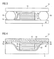
- the organic layers 1, 2, 3, 4a, 4b are mounted over a mounting side 90 of a substrate 9.
- the mounting side 90 is configured so that the various organic layers can be applied to the mounting side 90.
- the following layers are mounted on the substrate 9: first electrode 8a, first ambipolar injection layer 4a, first layer 1, charge carrier barrier layer 3, second layer 2, second ambipolar injection layer 4b, second electrode 8b, and a conversion agent layer 7. Operation and Construction the organic layers correspond to the embodiment according to FIG. 1 ,
- the electrodes 8a and 8b are applied over the whole area to the sides of the injection layers 4a, 4b facing away from the charge carrier barrier layer 3.
- the electrode 8b located on the side of the layer stack facing away from the substrate 9 is guided to the mounting side 90 of the substrate 9 such that no undesired electrical connections to layers other than the injection layer 4b occur.
- the electrode 8b is transparent to the radiation emitted during operation of the first and second layers 2.
- First 1 and second layer 2 emit in different spectral ranges.
- the conversion means 7 converts only a part of the radiation emitted, for example, by the second layer 2, so that overall a multi-colored emitting component 10 results which can emit approximately white light.
- the electrode 8a is designed to reflect the radiation emitted by the component 10.
- the electrodes 8a, 8b are guided on the mounting side 90 laterally away from the stack of layers 1, 2, 3, 4a, 4b in narrow paths, as in FIG FIG. 2b you can see.
- the component 10 also has a cover plate 91 in addition to the substrate 9.
- Substrate 9 and cover plate 91 which are formed, for example, from a soda-lime glass and configured in a planar manner, are mechanically connected to one another by means of a connecting means 95.
- the connecting means 95 is designed as a glass solder.
- the organic layers 1, 2, 3, 4a, 4b are also encapsulated.
- First 1 and second layer 2 emit light in the same spectral range.
- Substrate 9 and cover plate 91 are transparent to the radiation emitted by the first 1 and second layers 2 during operation, as is the connection means 95.
- the layer sequence of the organic layers 1, 2, 3, 4a, 4b corresponds to that in FIG FIG. 2 shown embodiment, wherein in the embodiment according to FIG. 3 the electrode 8a is also designed to be transparent to the emitted radiation, so that a component 10 which is transparent in at least parts of the visible spectral range results.
- the substrate 9 has a recess 92 in which the organic layers 1, 2, 3, 4a, 4b are mounted.
- the electrode 8a is applied flat on the mounting side 90 in the recess 92 and thereby forms a reflector for the radiation emitted by the component 10.
- the substrate 9 may be formed of a glass or a plastic film.
- the recess 92 can be created easily and cost-effectively via a stamping or stamping process. Characterized in that the active layers are in the recess 92, the cover plate 91 may be flat. As a result, the height or the extent of the connecting means 95 between cover plate 91 and substrate 9 can be significantly reduced, so that the lateral extent of the connecting means 95 is substantially greater than its vertical extent.
- Diffusion agent, conversion agent, filter medium or a substance to adjust the coefficient of thermal expansion be added.
- the electrode 8b is reflective and the electrode 8a is transparent to the radiation emitted by the component 10.
- the recess 92 can then be designed, for example, in the form of a lens in order to radiate the light emitted by the first 1 and second layer 2 approximately uniformly over a larger angular range.
- a layer is attached, for example, allows an adjustment of the refractive indices of organic layers 1, 2, 3, 4a, 4b and substrate 9 or even a planarization of those areas of the recess 92nd on which the various organic layers 1, 2, 3, 4a, 4b or the electrode 8a are applied.
- Such a planarization layer simplifies the manufacturing process of the component 10.
- an absorber material or a getter to be provided in the recess 92, for example the organic layers 1, 2, 3, 4a, 4b or also substrate 9 and cover plate 91 wrapped.
- substrate 9 and / or cover plate 91 may have structurings which, for example, improve the light extraction from the component 10.
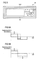
- an organic light-emitting component 10 is shown, which in addition to the stack of layers 1, 2, 3, 4, a control unit 5, which is applied between the substrate 9 and cover plate 91, and also located between cover plate 91 and substrate 9 sensor 50 comprises.
- Layer stack 1, 2, 3, 4, control unit 5 and sensor 50 are frame-like surrounded by a connecting means 95, the substrate 9 and cover plate 91 connects to each other.
- the electrodes 8 provide an electrical connection from outside the connecting means 95 to the interior and between the individual components.
- the organic layers 1, 2, 3, 4 are applied over a large area on the substrate 9 and occupy the majority of the surface of the substrate 9.
- the control unit 5 may also be based at least partially on organic materials and be mounted wholly or even partially within the frame of connecting means 95 on the substrate 9.
- a control unit 5 and a sensor 50 can be used for each layer stack 1, 2, 3, 4, a control unit 5 and a sensor 50. However, it is also possible to control a plurality of layer stacks 1, 2, 3, 4 via a single control unit 5.
- FIG. 6 a control scheme of the AC control unit 5 is illustrated. As in FIG. 6b shown, positive and negative phase have different durations.
- the voltage curve corresponds to a square-wave voltage, but can also be configured sinusoidal. By changing the effective voltages, the brightness of the light emitted by the component 10 can be adjusted.
- the control of hue and color saturation is in FIG. 6a explained. If the duty cycle, that is to say the ratio of the duration of the positive phase and the entire oscillation period, is changed via the control unit 5 and alternatively or additionally the effective voltage of the positive and / or negative phase is regulated, the color and saturation of the light emitted by the organic component 10 can be adjusted to be controlled. This applies in particular if first 1 and second layer 2 are designed in such a way that they emit light in different spectral ranges during operation.
- the control unit 5 can control both brightness and hue and color saturation independently of one another, for example with the aid of a sensor 50, as in the exemplary embodiment according to FIG FIG. 5 shown.
Landscapes
- Physics & Mathematics (AREA)
- Optics & Photonics (AREA)
- Engineering & Computer Science (AREA)
- Manufacturing & Machinery (AREA)
- Electroluminescent Light Sources (AREA)
Applications Claiming Priority (2)
| Application Number | Priority Date | Filing Date | Title |
|---|---|---|---|
| DE102008025755A DE102008025755A1 (de) | 2008-05-29 | 2008-05-29 | Organisches Licht emittierendes Bauteil und Leuchtmittel mit einem solchen Bauteil |
| PCT/DE2009/000644 WO2009143801A1 (de) | 2008-05-29 | 2009-05-07 | Organisches licht emittierendes bauteil und leuchtmittel mit einem solchen bauteil |
Publications (2)
| Publication Number | Publication Date |
|---|---|
| EP2281317A1 EP2281317A1 (de) | 2011-02-09 |
| EP2281317B1 true EP2281317B1 (de) | 2014-11-19 |
Family
ID=41136769
Family Applications (1)
| Application Number | Title | Priority Date | Filing Date |
|---|---|---|---|
| EP09753517.3A Not-in-force EP2281317B1 (de) | 2008-05-29 | 2009-05-07 | Organisches licht emittierendes bauteil und leuchtmittel mit einem solchen bauteil |
Country Status (7)
Families Citing this family (9)
| Publication number | Priority date | Publication date | Assignee | Title |
|---|---|---|---|---|
| DE102008045029B4 (de) * | 2007-09-28 | 2016-12-22 | Osram Oled Gmbh | Strahlungsemittierendes Bauelement sowie Betriebsverfahren und Betriebsanordnung |
| DE102011084276B4 (de) | 2011-10-11 | 2019-10-10 | Osram Oled Gmbh | Verkapselung für ein organisches elektronisches bauelement, ein organisches elektronisches bauelement mit der verkapselung und ein verfahren zur herstellung eines organischen elektronischen bauelements mit der verkapselung |
| FR2988638B1 (fr) | 2012-03-27 | 2015-02-06 | Sidel Participations | Tuyere pour le formage de recipients equipee d'un nez interchangeable dans lequel sont emprisonnes des elements adaptes au format du col du recipient |
| JP2015215940A (ja) * | 2012-08-17 | 2015-12-03 | 出光興産株式会社 | 発光装置、電子機器および発光装置の製造方法 |
| JP6294417B2 (ja) * | 2016-09-01 | 2018-03-14 | 日機装株式会社 | 光半導体装置および光半導体装置の製造方法 |
| CN106255277A (zh) * | 2016-09-30 | 2016-12-21 | 福州大学 | 基于驱动电路提高oled发光效率的方法 |
| CN109686851A (zh) * | 2018-12-26 | 2019-04-26 | 上海晶合光电科技有限公司 | 一种有机发光二极管及其制备方法 |
| EP4012794A1 (en) * | 2020-12-11 | 2022-06-15 | Julius-Maximilians-Universität Würzburg | Emission of electromagnetic radiation and control of properties of the emitted electromagnetic radiation |
| CN113013348B (zh) * | 2021-04-29 | 2024-10-29 | 武汉华美晨曦光电有限责任公司 | 一种oled器件及光源组件 |
Family Cites Families (24)
| Publication number | Priority date | Publication date | Assignee | Title |
|---|---|---|---|---|
| DE10132329B4 (de) * | 2001-06-29 | 2005-02-24 | Schrader, Karl-Heinz Sigurd, Dr. | Lichtemittierende Vorrichtung und Verfahren zu ihrer Herstellung |
| JP3983037B2 (ja) * | 2001-11-22 | 2007-09-26 | 株式会社半導体エネルギー研究所 | 発光装置およびその作製方法 |
| US6809481B2 (en) * | 2002-02-28 | 2004-10-26 | Semiconductor Energy Laboratory Co., Ltd. | Light emitting device and electric device using the same |
| US7049757B2 (en) | 2002-08-05 | 2006-05-23 | General Electric Company | Series connected OLED structure and fabrication method |
| TWI272874B (en) * | 2002-08-09 | 2007-02-01 | Semiconductor Energy Lab | Organic electroluminescent device |
| US7052351B2 (en) | 2002-12-31 | 2006-05-30 | Eastman Kodak Company | Using hole- or electron-blocking layers in color OLEDS |
| CN1781340A (zh) | 2003-02-27 | 2006-05-31 | 株式会社丰田自动织机 | 有机电致发光元件 |
| TWI265750B (en) | 2003-02-27 | 2006-11-01 | Toyota Jidoshokki Kk | Organic electro-luminescence devices |
| US8704253B2 (en) * | 2003-03-25 | 2014-04-22 | Rohm Co., Ltd. | Light-emitting device and organic electroluminescence light-emitting device |
| KR101164687B1 (ko) * | 2003-07-02 | 2012-07-11 | 이데미쓰 고산 가부시키가이샤 | 유기 전기발광 소자 및 이를 이용한 표시 장치 |
| JP2005100921A (ja) | 2003-08-22 | 2005-04-14 | Sony Corp | 有機el素子および表示装置 |
| CN100534246C (zh) | 2003-08-22 | 2009-08-26 | 索尼株式会社 | 有机电致发光器件及显示器 |
| JP4276109B2 (ja) * | 2004-03-01 | 2009-06-10 | ローム株式会社 | 有機エレクトロルミネッセント素子 |
| JP2005259492A (ja) | 2004-03-11 | 2005-09-22 | Fuji Photo Film Co Ltd | 有機電界発光素子 |
| US7952089B2 (en) * | 2004-10-22 | 2011-05-31 | Semiconductor Energy Laboratory Co., Ltd. | Composite material and light emitting element |
| US7646010B2 (en) * | 2004-11-26 | 2010-01-12 | Semiconductor Energy Laboratory Co., Ltd. | Light-emitting element, light-emitting device, and electronic device |
| JP2006164708A (ja) | 2004-12-06 | 2006-06-22 | Semiconductor Energy Lab Co Ltd | 電子機器および発光装置 |
| US20060145599A1 (en) | 2005-01-04 | 2006-07-06 | Reza Stegamat | OLEDs with phosphors |
| JP4939809B2 (ja) * | 2005-01-21 | 2012-05-30 | 株式会社半導体エネルギー研究所 | 発光装置 |
| US8148891B2 (en) | 2005-10-04 | 2012-04-03 | Universal Display Corporation | Electron impeding layer for high efficiency phosphorescent OLEDs |
| US7659544B2 (en) * | 2005-12-23 | 2010-02-09 | Hong Kong Applied Science And Technology Research Institute Co., Ltd. | Light emitting device with at least two alternately driven light emitting diodes |
| US8026512B2 (en) * | 2006-11-16 | 2011-09-27 | Panasonic Corporation | Mobility engineered electroluminescent devices |
| DE102007058005B4 (de) * | 2007-09-25 | 2018-05-17 | Osram Oled Gmbh | Strahlungsemittierende Vorrichtung und Verfahren zu deren Herstellung |
| EP2068380B1 (de) * | 2007-10-15 | 2011-08-17 | Novaled AG | Organisches elektrolumineszentes Bauelement |
-
2008
- 2008-05-29 DE DE102008025755A patent/DE102008025755A1/de not_active Withdrawn
-
2009
- 2009-05-07 US US12/995,182 patent/US8686440B2/en active Active
- 2009-05-07 CN CN200980109076.5A patent/CN101971385B/zh not_active Expired - Fee Related
- 2009-05-07 WO PCT/DE2009/000644 patent/WO2009143801A1/de active Application Filing
- 2009-05-07 KR KR1020107020191A patent/KR101593249B1/ko not_active Expired - Fee Related
- 2009-05-07 JP JP2011510820A patent/JP5389163B2/ja not_active Expired - Fee Related
- 2009-05-07 EP EP09753517.3A patent/EP2281317B1/de not_active Not-in-force
Also Published As
| Publication number | Publication date |
|---|---|
| JP5389163B2 (ja) | 2014-01-15 |
| KR101593249B1 (ko) | 2016-02-11 |
| CN101971385A (zh) | 2011-02-09 |
| WO2009143801A1 (de) | 2009-12-03 |
| JP2011521482A (ja) | 2011-07-21 |
| KR20110021716A (ko) | 2011-03-04 |
| CN101971385B (zh) | 2014-10-01 |
| EP2281317A1 (de) | 2011-02-09 |
| US8686440B2 (en) | 2014-04-01 |
| US20110266572A1 (en) | 2011-11-03 |
| DE102008025755A1 (de) | 2009-12-03 |
Similar Documents
| Publication | Publication Date | Title |
|---|---|---|
| EP2281317B1 (de) | Organisches licht emittierendes bauteil und leuchtmittel mit einem solchen bauteil | |
| EP2126998B1 (de) | Oled mit farbkonversion | |
| DE102011086168B4 (de) | Organisches Licht emittierendes Bauelement und Verfahren zur Herstellung eines organischen optoelektronischen Bauelements | |
| EP3022782B1 (de) | Verfahren zum betrieb eines organischen licht emittierenden bauelements | |
| EP2220693B1 (de) | Strahlungsemittierende vorrichtung | |
| DE102006000770A1 (de) | OLEDs mit Leuchtstoffen | |
| DE102006045702A1 (de) | Optoelektronisches Bauteil | |
| EP2715826B1 (de) | Organisches elektrolumineszierendes bauelement | |
| WO2009036718A1 (de) | Optoelektronisches bauteil | |
| WO2014067853A1 (de) | Organisches optoelektronisches bauelement und verfahren zum betrieb des organischen optoelektronischen bauelements | |
| DE102013107225A1 (de) | Optoelektronische Bauelementanordnung, Verfahren zum Herstellen einer optoelektronischen Bauelementanordnung, Verfahren zum Betreiben einer optoelektronischen Bauelementanordnung | |
| DE112014000564B4 (de) | Verfahren zum Betrieb eines organischen optoelektronischen Bauelements | |
| EP3516710A1 (de) | Diffusionslimitierende elektroaktive barriereschicht für ein optoelektronisches bauteil | |
| DE102012223162A1 (de) | Flächenlichtsystem | |
| DE102013110483A1 (de) | Optoelektronische Bauelementevorrichtung und Verfahren zum Betreiben eines optoelektronischen Bauelementes | |
| WO2017080790A1 (de) | Organische, lichtemittierende bauelementevorrichtung, verfahren zum herstellen einer organischen, lichtemittierenden bauelementevorrichtung und verfahren zum betreiben einer organischen, lichtemittierenden bauelementevorrichtung | |
| WO2014067852A1 (de) | Organisches optoelektronisches bauelement und verfahren zum betrieb des organischen optoelektronischen bauelements | |
| WO2015007782A1 (de) | Verfahren zum betrieb eines organischen licht emittierenden bauelements und leuchtvorrichtung zur durchführung des verfahrens | |
| DE102013106944A1 (de) | Optoelektronische Bauelementevorrichtung, Verfahren zum Herstellen einer optoelektronischen Bauelementevorrichtung und Verfahren zum Betreiben einer optoelektronischen Bauelementevorrichtung | |
| WO2014067851A1 (de) | Organisches optoelektronisches bauelement und verfahren zum betrieb des organischen optoelektronischen bauelements | |
| DE102007062040A1 (de) | Strahlungsemittierende Vorrichtung | |
| DE102014103754A1 (de) | Verfahren zur Steuerung eines organischen Licht emittierenden Bauelements und organisches Licht emittierendes Bauelement | |
| DE102014103751A1 (de) | Organisches strahlungsemittierendes Bauelement | |
| WO2015181048A1 (de) | Transparentes organisches licht emittierendes bauelement und licht emittierende vorrichtung mit einem transparenten organischen licht emittierenden bauelement | |
| WO2014067870A1 (de) | Verfahren zum betrieb eines organischen optoelektronischen bauelements |
Legal Events
| Date | Code | Title | Description |
|---|---|---|---|
| PUAI | Public reference made under article 153(3) epc to a published international application that has entered the european phase |
Free format text: ORIGINAL CODE: 0009012 |
|
| 17P | Request for examination filed |
Effective date: 20100809 |
|
| AK | Designated contracting states |
Kind code of ref document: A1 Designated state(s): AT BE BG CH CY CZ DE DK EE ES FI FR GB GR HR HU IE IS IT LI LT LU LV MC MK MT NL NO PL PT RO SE SI SK TR |
|
| AX | Request for extension of the european patent |
Extension state: AL BA RS |
|
| DAX | Request for extension of the european patent (deleted) | ||
| GRAP | Despatch of communication of intention to grant a patent |
Free format text: ORIGINAL CODE: EPIDOSNIGR1 |
|
| INTG | Intention to grant announced |
Effective date: 20140717 |
|
| GRAS | Grant fee paid |
Free format text: ORIGINAL CODE: EPIDOSNIGR3 |
|
| GRAA | (expected) grant |
Free format text: ORIGINAL CODE: 0009210 |
|
| AK | Designated contracting states |
Kind code of ref document: B1 Designated state(s): AT BE BG CH CY CZ DE DK EE ES FI FR GB GR HR HU IE IS IT LI LT LU LV MC MK MT NL NO PL PT RO SE SI SK TR |
|
| REG | Reference to a national code |
Ref country code: GB Ref legal event code: FG4D Free format text: NOT ENGLISH |
|
| REG | Reference to a national code |
Ref country code: CH Ref legal event code: EP |
|
| REG | Reference to a national code |
Ref country code: AT Ref legal event code: REF Ref document number: 697476 Country of ref document: AT Kind code of ref document: T Effective date: 20141215 |
|
| REG | Reference to a national code |
Ref country code: IE Ref legal event code: FG4D Free format text: LANGUAGE OF EP DOCUMENT: GERMAN |
|
| REG | Reference to a national code |
Ref country code: DE Ref legal event code: R096 Ref document number: 502009010249 Country of ref document: DE Effective date: 20141224 |
|
| REG | Reference to a national code |
Ref country code: NL Ref legal event code: VDEP Effective date: 20141119 |
|
| REG | Reference to a national code |
Ref country code: LT Ref legal event code: MG4D |
|
| PG25 | Lapsed in a contracting state [announced via postgrant information from national office to epo] |
Ref country code: NO Free format text: LAPSE BECAUSE OF FAILURE TO SUBMIT A TRANSLATION OF THE DESCRIPTION OR TO PAY THE FEE WITHIN THE PRESCRIBED TIME-LIMIT Effective date: 20150219 Ref country code: ES Free format text: LAPSE BECAUSE OF FAILURE TO SUBMIT A TRANSLATION OF THE DESCRIPTION OR TO PAY THE FEE WITHIN THE PRESCRIBED TIME-LIMIT Effective date: 20141119 Ref country code: LT Free format text: LAPSE BECAUSE OF FAILURE TO SUBMIT A TRANSLATION OF THE DESCRIPTION OR TO PAY THE FEE WITHIN THE PRESCRIBED TIME-LIMIT Effective date: 20141119 Ref country code: NL Free format text: LAPSE BECAUSE OF FAILURE TO SUBMIT A TRANSLATION OF THE DESCRIPTION OR TO PAY THE FEE WITHIN THE PRESCRIBED TIME-LIMIT Effective date: 20141119 Ref country code: IS Free format text: LAPSE BECAUSE OF FAILURE TO SUBMIT A TRANSLATION OF THE DESCRIPTION OR TO PAY THE FEE WITHIN THE PRESCRIBED TIME-LIMIT Effective date: 20150319 Ref country code: PT Free format text: LAPSE BECAUSE OF FAILURE TO SUBMIT A TRANSLATION OF THE DESCRIPTION OR TO PAY THE FEE WITHIN THE PRESCRIBED TIME-LIMIT Effective date: 20150319 Ref country code: FI Free format text: LAPSE BECAUSE OF FAILURE TO SUBMIT A TRANSLATION OF THE DESCRIPTION OR TO PAY THE FEE WITHIN THE PRESCRIBED TIME-LIMIT Effective date: 20141119 |
|
| PG25 | Lapsed in a contracting state [announced via postgrant information from national office to epo] |
Ref country code: PL Free format text: LAPSE BECAUSE OF FAILURE TO SUBMIT A TRANSLATION OF THE DESCRIPTION OR TO PAY THE FEE WITHIN THE PRESCRIBED TIME-LIMIT Effective date: 20141119 Ref country code: HR Free format text: LAPSE BECAUSE OF FAILURE TO SUBMIT A TRANSLATION OF THE DESCRIPTION OR TO PAY THE FEE WITHIN THE PRESCRIBED TIME-LIMIT Effective date: 20141119 Ref country code: GR Free format text: LAPSE BECAUSE OF FAILURE TO SUBMIT A TRANSLATION OF THE DESCRIPTION OR TO PAY THE FEE WITHIN THE PRESCRIBED TIME-LIMIT Effective date: 20150220 Ref country code: LV Free format text: LAPSE BECAUSE OF FAILURE TO SUBMIT A TRANSLATION OF THE DESCRIPTION OR TO PAY THE FEE WITHIN THE PRESCRIBED TIME-LIMIT Effective date: 20141119 Ref country code: CY Free format text: LAPSE BECAUSE OF FAILURE TO SUBMIT A TRANSLATION OF THE DESCRIPTION OR TO PAY THE FEE WITHIN THE PRESCRIBED TIME-LIMIT Effective date: 20141119 Ref country code: SE Free format text: LAPSE BECAUSE OF FAILURE TO SUBMIT A TRANSLATION OF THE DESCRIPTION OR TO PAY THE FEE WITHIN THE PRESCRIBED TIME-LIMIT Effective date: 20141119 |
|
| PG25 | Lapsed in a contracting state [announced via postgrant information from national office to epo] |
Ref country code: DK Free format text: LAPSE BECAUSE OF FAILURE TO SUBMIT A TRANSLATION OF THE DESCRIPTION OR TO PAY THE FEE WITHIN THE PRESCRIBED TIME-LIMIT Effective date: 20141119 Ref country code: CZ Free format text: LAPSE BECAUSE OF FAILURE TO SUBMIT A TRANSLATION OF THE DESCRIPTION OR TO PAY THE FEE WITHIN THE PRESCRIBED TIME-LIMIT Effective date: 20141119 Ref country code: RO Free format text: LAPSE BECAUSE OF FAILURE TO SUBMIT A TRANSLATION OF THE DESCRIPTION OR TO PAY THE FEE WITHIN THE PRESCRIBED TIME-LIMIT Effective date: 20141119 Ref country code: EE Free format text: LAPSE BECAUSE OF FAILURE TO SUBMIT A TRANSLATION OF THE DESCRIPTION OR TO PAY THE FEE WITHIN THE PRESCRIBED TIME-LIMIT Effective date: 20141119 Ref country code: SK Free format text: LAPSE BECAUSE OF FAILURE TO SUBMIT A TRANSLATION OF THE DESCRIPTION OR TO PAY THE FEE WITHIN THE PRESCRIBED TIME-LIMIT Effective date: 20141119 |
|
| REG | Reference to a national code |
Ref country code: DE Ref legal event code: R097 Ref document number: 502009010249 Country of ref document: DE |
|
| RAP2 | Party data changed (patent owner data changed or rights of a patent transferred) |
Owner name: OSRAM OLED GMBH |
|
| PLBE | No opposition filed within time limit |
Free format text: ORIGINAL CODE: 0009261 |
|
| STAA | Information on the status of an ep patent application or granted ep patent |
Free format text: STATUS: NO OPPOSITION FILED WITHIN TIME LIMIT |
|
| 26N | No opposition filed |
Effective date: 20150820 |
|
| PG25 | Lapsed in a contracting state [announced via postgrant information from national office to epo] |
Ref country code: IT Free format text: LAPSE BECAUSE OF FAILURE TO SUBMIT A TRANSLATION OF THE DESCRIPTION OR TO PAY THE FEE WITHIN THE PRESCRIBED TIME-LIMIT Effective date: 20141119 |
|
| REG | Reference to a national code |
Ref country code: CH Ref legal event code: PL |
|
| PG25 | Lapsed in a contracting state [announced via postgrant information from national office to epo] |
Ref country code: MC Free format text: LAPSE BECAUSE OF FAILURE TO SUBMIT A TRANSLATION OF THE DESCRIPTION OR TO PAY THE FEE WITHIN THE PRESCRIBED TIME-LIMIT Effective date: 20141119 Ref country code: LI Free format text: LAPSE BECAUSE OF NON-PAYMENT OF DUE FEES Effective date: 20150531 Ref country code: LU Free format text: LAPSE BECAUSE OF FAILURE TO SUBMIT A TRANSLATION OF THE DESCRIPTION OR TO PAY THE FEE WITHIN THE PRESCRIBED TIME-LIMIT Effective date: 20150507 Ref country code: CH Free format text: LAPSE BECAUSE OF NON-PAYMENT OF DUE FEES Effective date: 20150531 |
|
| REG | Reference to a national code |
Ref country code: IE Ref legal event code: MM4A |
|
| PG25 | Lapsed in a contracting state [announced via postgrant information from national office to epo] |
Ref country code: SI Free format text: LAPSE BECAUSE OF FAILURE TO SUBMIT A TRANSLATION OF THE DESCRIPTION OR TO PAY THE FEE WITHIN THE PRESCRIBED TIME-LIMIT Effective date: 20141119 |
|
| PG25 | Lapsed in a contracting state [announced via postgrant information from national office to epo] |
Ref country code: IE Free format text: LAPSE BECAUSE OF NON-PAYMENT OF DUE FEES Effective date: 20150507 |
|
| REG | Reference to a national code |
Ref country code: FR Ref legal event code: PLFP Year of fee payment: 8 |
|
| REG | Reference to a national code |
Ref country code: AT Ref legal event code: MM01 Ref document number: 697476 Country of ref document: AT Kind code of ref document: T Effective date: 20150507 |
|
| PG25 | Lapsed in a contracting state [announced via postgrant information from national office to epo] |
Ref country code: AT Free format text: LAPSE BECAUSE OF NON-PAYMENT OF DUE FEES Effective date: 20150507 |
|
| REG | Reference to a national code |
Ref country code: DE Ref legal event code: R081 Ref document number: 502009010249 Country of ref document: DE Owner name: OSRAM OLED GMBH, DE Free format text: FORMER OWNER: OSRAM OPTO SEMICONDUCTORS GESELLSCHAFT MIT BESCHRAENKTER HAFTUNG, 93055 REGENSBURG, DE Ref country code: DE Ref legal event code: R082 Ref document number: 502009010249 Country of ref document: DE Representative=s name: EPPING HERMANN FISCHER, PATENTANWALTSGESELLSCH, DE Ref country code: DE Ref legal event code: R081 Ref document number: 502009010249 Country of ref document: DE Owner name: OSRAM OLED GMBH, DE Free format text: FORMER OWNER: OSRAM OPTO SEMICONDUCTORS GMBH, 93055 REGENSBURG, DE Ref country code: DE Ref legal event code: R082 Ref document number: 502009010249 Country of ref document: DE Representative=s name: EPPING HERMANN FISCHER PATENTANWALTSGESELLSCHA, DE |
|
| PG25 | Lapsed in a contracting state [announced via postgrant information from national office to epo] |
Ref country code: MT Free format text: LAPSE BECAUSE OF FAILURE TO SUBMIT A TRANSLATION OF THE DESCRIPTION OR TO PAY THE FEE WITHIN THE PRESCRIBED TIME-LIMIT Effective date: 20141119 |
|
| REG | Reference to a national code |
Ref country code: FR Ref legal event code: PLFP Year of fee payment: 9 |
|
| PG25 | Lapsed in a contracting state [announced via postgrant information from national office to epo] |
Ref country code: HU Free format text: LAPSE BECAUSE OF FAILURE TO SUBMIT A TRANSLATION OF THE DESCRIPTION OR TO PAY THE FEE WITHIN THE PRESCRIBED TIME-LIMIT; INVALID AB INITIO Effective date: 20090507 Ref country code: BG Free format text: LAPSE BECAUSE OF FAILURE TO SUBMIT A TRANSLATION OF THE DESCRIPTION OR TO PAY THE FEE WITHIN THE PRESCRIBED TIME-LIMIT Effective date: 20141119 |
|
| PG25 | Lapsed in a contracting state [announced via postgrant information from national office to epo] |
Ref country code: BE Free format text: LAPSE BECAUSE OF NON-PAYMENT OF DUE FEES Effective date: 20150531 |
|
| PGFP | Annual fee paid to national office [announced via postgrant information from national office to epo] |
Ref country code: FR Payment date: 20170523 Year of fee payment: 9 Ref country code: GB Payment date: 20170519 Year of fee payment: 9 |
|
| REG | Reference to a national code |
Ref country code: GB Ref legal event code: 732E Free format text: REGISTERED BETWEEN 20170706 AND 20170715 |
|
| PG25 | Lapsed in a contracting state [announced via postgrant information from national office to epo] |
Ref country code: TR Free format text: LAPSE BECAUSE OF FAILURE TO SUBMIT A TRANSLATION OF THE DESCRIPTION OR TO PAY THE FEE WITHIN THE PRESCRIBED TIME-LIMIT Effective date: 20141119 |
|
| PG25 | Lapsed in a contracting state [announced via postgrant information from national office to epo] |
Ref country code: MK Free format text: LAPSE BECAUSE OF FAILURE TO SUBMIT A TRANSLATION OF THE DESCRIPTION OR TO PAY THE FEE WITHIN THE PRESCRIBED TIME-LIMIT Effective date: 20141119 |
|
| GBPC | Gb: european patent ceased through non-payment of renewal fee |
Effective date: 20180507 |
|
| PG25 | Lapsed in a contracting state [announced via postgrant information from national office to epo] |
Ref country code: FR Free format text: LAPSE BECAUSE OF NON-PAYMENT OF DUE FEES Effective date: 20180531 Ref country code: GB Free format text: LAPSE BECAUSE OF NON-PAYMENT OF DUE FEES Effective date: 20180507 |
|
| PGFP | Annual fee paid to national office [announced via postgrant information from national office to epo] |
Ref country code: DE Payment date: 20210526 Year of fee payment: 13 |
|
| REG | Reference to a national code |
Ref country code: DE Ref legal event code: R079 Ref document number: 502009010249 Country of ref document: DE Free format text: PREVIOUS MAIN CLASS: H01L0051500000 Ipc: H10K0050000000 |
|
| REG | Reference to a national code |
Ref country code: DE Ref legal event code: R119 Ref document number: 502009010249 Country of ref document: DE |
|
| PG25 | Lapsed in a contracting state [announced via postgrant information from national office to epo] |
Ref country code: DE Free format text: LAPSE BECAUSE OF NON-PAYMENT OF DUE FEES Effective date: 20221201 |