EP2281315B1 - Halbleiteranordnung - Google Patents
Halbleiteranordnung Download PDFInfo
- Publication number
- EP2281315B1 EP2281315B1 EP09753511.6A EP09753511A EP2281315B1 EP 2281315 B1 EP2281315 B1 EP 2281315B1 EP 09753511 A EP09753511 A EP 09753511A EP 2281315 B1 EP2281315 B1 EP 2281315B1
- Authority
- EP
- European Patent Office
- Prior art keywords
- chip
- semiconductor chip
- semiconductor
- radiation
- connection points
- Prior art date
- Legal status (The legal status is an assumption and is not a legal conclusion. Google has not performed a legal analysis and makes no representation as to the accuracy of the status listed.)
- Active
Links
Images
Classifications
-
- H—ELECTRICITY
- H10—SEMICONDUCTOR DEVICES; ELECTRIC SOLID-STATE DEVICES NOT OTHERWISE PROVIDED FOR
- H10H—INORGANIC LIGHT-EMITTING SEMICONDUCTOR DEVICES HAVING POTENTIAL BARRIERS
- H10H20/00—Individual inorganic light-emitting semiconductor devices having potential barriers, e.g. light-emitting diodes [LED]
- H10H20/80—Constructional details
- H10H20/85—Packages
- H10H20/852—Encapsulations
- H10H20/853—Encapsulations characterised by their shape
-
- H—ELECTRICITY
- H10—SEMICONDUCTOR DEVICES; ELECTRIC SOLID-STATE DEVICES NOT OTHERWISE PROVIDED FOR
- H10H—INORGANIC LIGHT-EMITTING SEMICONDUCTOR DEVICES HAVING POTENTIAL BARRIERS
- H10H20/00—Individual inorganic light-emitting semiconductor devices having potential barriers, e.g. light-emitting diodes [LED]
- H10H20/80—Constructional details
- H10H20/85—Packages
- H10H20/855—Optical field-shaping means, e.g. lenses
-
- H—ELECTRICITY
- H01—ELECTRIC ELEMENTS
- H01L—SEMICONDUCTOR DEVICES NOT COVERED BY CLASS H10
- H01L2224/00—Indexing scheme for arrangements for connecting or disconnecting semiconductor or solid-state bodies and methods related thereto as covered by H01L24/00
- H01L2224/01—Means for bonding being attached to, or being formed on, the surface to be connected, e.g. chip-to-package, die-attach, "first-level" interconnects; Manufacturing methods related thereto
- H01L2224/42—Wire connectors; Manufacturing methods related thereto
- H01L2224/47—Structure, shape, material or disposition of the wire connectors after the connecting process
- H01L2224/48—Structure, shape, material or disposition of the wire connectors after the connecting process of an individual wire connector
- H01L2224/4805—Shape
- H01L2224/4809—Loop shape
- H01L2224/48091—Arched
-
- H—ELECTRICITY
- H01—ELECTRIC ELEMENTS
- H01L—SEMICONDUCTOR DEVICES NOT COVERED BY CLASS H10
- H01L25/00—Assemblies consisting of a plurality of semiconductor or other solid state devices
- H01L25/03—Assemblies consisting of a plurality of semiconductor or other solid state devices all the devices being of a type provided for in a single subclass of subclasses H10B, H10D, H10F, H10H, H10K or H10N, e.g. assemblies of rectifier diodes
- H01L25/04—Assemblies consisting of a plurality of semiconductor or other solid state devices all the devices being of a type provided for in a single subclass of subclasses H10B, H10D, H10F, H10H, H10K or H10N, e.g. assemblies of rectifier diodes the devices not having separate containers
- H01L25/041—Assemblies consisting of a plurality of semiconductor or other solid state devices all the devices being of a type provided for in a single subclass of subclasses H10B, H10D, H10F, H10H, H10K or H10N, e.g. assemblies of rectifier diodes the devices not having separate containers the devices being of a type provided for in subclass H10F
- H01L25/042—Assemblies consisting of a plurality of semiconductor or other solid state devices all the devices being of a type provided for in a single subclass of subclasses H10B, H10D, H10F, H10H, H10K or H10N, e.g. assemblies of rectifier diodes the devices not having separate containers the devices being of a type provided for in subclass H10F the devices being arranged next to each other
-
- H—ELECTRICITY
- H01—ELECTRIC ELEMENTS
- H01L—SEMICONDUCTOR DEVICES NOT COVERED BY CLASS H10
- H01L25/00—Assemblies consisting of a plurality of semiconductor or other solid state devices
- H01L25/03—Assemblies consisting of a plurality of semiconductor or other solid state devices all the devices being of a type provided for in a single subclass of subclasses H10B, H10D, H10F, H10H, H10K or H10N, e.g. assemblies of rectifier diodes
- H01L25/04—Assemblies consisting of a plurality of semiconductor or other solid state devices all the devices being of a type provided for in a single subclass of subclasses H10B, H10D, H10F, H10H, H10K or H10N, e.g. assemblies of rectifier diodes the devices not having separate containers
- H01L25/075—Assemblies consisting of a plurality of semiconductor or other solid state devices all the devices being of a type provided for in a single subclass of subclasses H10B, H10D, H10F, H10H, H10K or H10N, e.g. assemblies of rectifier diodes the devices not having separate containers the devices being of a type provided for in group H10H20/00
- H01L25/0753—Assemblies consisting of a plurality of semiconductor or other solid state devices all the devices being of a type provided for in a single subclass of subclasses H10B, H10D, H10F, H10H, H10K or H10N, e.g. assemblies of rectifier diodes the devices not having separate containers the devices being of a type provided for in group H10H20/00 the devices being arranged next to each other
-
- H—ELECTRICITY
- H10—SEMICONDUCTOR DEVICES; ELECTRIC SOLID-STATE DEVICES NOT OTHERWISE PROVIDED FOR
- H10H—INORGANIC LIGHT-EMITTING SEMICONDUCTOR DEVICES HAVING POTENTIAL BARRIERS
- H10H20/00—Individual inorganic light-emitting semiconductor devices having potential barriers, e.g. light-emitting diodes [LED]
- H10H20/80—Constructional details
- H10H20/83—Electrodes
- H10H20/831—Electrodes characterised by their shape
-
- H—ELECTRICITY
- H10—SEMICONDUCTOR DEVICES; ELECTRIC SOLID-STATE DEVICES NOT OTHERWISE PROVIDED FOR
- H10H—INORGANIC LIGHT-EMITTING SEMICONDUCTOR DEVICES HAVING POTENTIAL BARRIERS
- H10H20/00—Individual inorganic light-emitting semiconductor devices having potential barriers, e.g. light-emitting diodes [LED]
- H10H20/80—Constructional details
- H10H20/85—Packages
- H10H20/855—Optical field-shaping means, e.g. lenses
- H10H20/856—Reflecting means
-
- H—ELECTRICITY
- H10—SEMICONDUCTOR DEVICES; ELECTRIC SOLID-STATE DEVICES NOT OTHERWISE PROVIDED FOR
- H10H—INORGANIC LIGHT-EMITTING SEMICONDUCTOR DEVICES HAVING POTENTIAL BARRIERS
- H10H20/00—Individual inorganic light-emitting semiconductor devices having potential barriers, e.g. light-emitting diodes [LED]
- H10H20/80—Constructional details
- H10H20/85—Packages
- H10H20/857—Interconnections, e.g. lead-frames, bond wires or solder balls
Definitions
- a semiconductor device with an optoelectronic semiconductor chip is specified.
- Optoelectronic semiconductor chips for example in the form of photodiodes or of light-emitting diodes, have found widespread use in recent years. Some aspects that promote the spread of optoelectronic semiconductor chips are their high efficiency, robustness against external environmental influences such as moisture or mechanical stress, long life, compact design and various design options, and this with relatively low production costs. Often crucial for these properties is the house of the semiconductor chip, which is therefore usually given great attention.
- optoelectronic semiconductor chips and in particular light emitting diodes and laser diodes, occupy a predominant position are, for example, the backlighting of displays or display devices.
- optoelectronic semiconductor chips are also used in illumination devices for projection purposes, in headlights or directional radiators, or in general lighting.
- the publication US 2005/0280016 A1 relates to a PCB-based, surface-mountable light-emitting diode.
- a surface mountable light emitting diode is in the document US 6,345,903 B described.
- a luminescent ceramic for light-emitting diodes can be found in the document US 2005/0269582 A1 ,
- a white light source is in the document US 2005/0093430 A1 disclosed.
- a light emitting diode with improved light extraction is in the document EP 1 191 608 A2 specified.
- An object to be solved is to provide a semiconductor device which has particularly good optical properties and has only a small footprint.
- the semiconductor device has a mounting side through which the semiconductor device is connected to an external carrier not belonging to the semiconductor device, such as a circuit board or a ceramic.
- the semiconductor device comprises at least one optoelectronic semiconductor chip.
- the semiconductor chip has a chip top and bottom sides that are substantially opposite each other.
- the semiconductor chip comprises a light emitting diode or laser diode which emits light approximately in the near UV, in the visible or in the near infrared spectral range.
- the semiconductor chip is configured, for example, as a sensor in the form of a photodiode, for example, for visible or near-infrared light.
- the semiconductor chip is designed as a flip-chip or as a thin-film chip.
- the contact points of the chip, via which it is electrically contacted, are limited to the chip underside.
- the semiconductor device comprises an at least partially radiation-transmissive body. That is, the body is transparent or transmissive to at least a portion of the radiation to be received or emitted by the semiconductor chip.
- the body has a body bottom on which the semiconductor chip is mounted.
- the chip top of the semiconductor chip faces at least parts of the body bottom.
- the underside of the body may be substantially flat or may have structures, such as recesses.
- the semiconductor chip can be in direct contact with the underside of the body or can also be attached to it via at least one intermediate layer.
- the semiconductor device comprises at least two electrical connection points, which serve to electrically contact the optoelectronic semiconductor chip.
- the Terminals can be an integral part of the semiconductor chip, as well as they can be attached as separate components to the chip, either in direct contact with this or by means of an intermediate carrier.
- the connection points do not project beyond the radiation-transmissive body laterally. In other words, the connection points in directions along the chip underside and / or the underside of the body do not extend beyond the radiation-transmissive body. That is, the largest lateral extent of the semiconductor device, approximately parallel to the chip bottom, is given by the radiation-transmissive body or by the semiconductor chip.
- the connection points limit the semiconductor device in the direction of its mounting side. That is, neither radiation-transmissive body nor semiconductor chip protrude beyond the connection points in the direction of the mounting side. In other words, the semiconductor device is limited in directions transverse to the chip bottom side and / or body bottom side by the connection points.
- the semiconductor device is surface mountable. This means that when connecting the semiconductor device, for example to an external carrier, no through-connection through the external carrier, for example in the form of solder pins, is necessary.
- connecting the semiconductor device is preferably placed on a surface, for example, the external support, without penetrating this surface, before a mechanical connection between the carrier and semiconductor device takes place, for example by means of soldering or gluing.
- the mounting of the semiconductor device is simplified.
- the steps may be reduced in the design of about an external carrier.
- the semiconductor device comprises a mounting side, at least one optoelectronic semiconductor chip having opposite chip top and bottom sides, and at least one at least partially radiation-transmissive body having a body bottom to which the semiconductor chip is attached so that the chip top faces the body bottom.
- the semiconductor arrangement comprises at least two electrical connection points for electrically contacting the optoelectronic semiconductor chip, wherein the connection points do not laterally project beyond the body and with their side facing away from the semiconductor chip bound the semiconductor arrangement at the mounting side thereof, and wherein the semiconductor arrangement is surface mountable.
- such a semiconductor device makes it possible to produce very compact and space-saving components, for example because the lateral extent of the semiconductor device can be limited by the lateral extent of the radiation-transmissive body. Due to the small number of components of the semiconductor device and their production can be designed efficiently and take place with reduced production costs. At the same time it is ensured that the specific configuration of the semiconductor device can be handled flexibly.
- the semiconductor chip is connected to the prefabricated radiation-transmissive body with an at least partially radiation-permeable adhesive bond.
- the adhesive connection a permanent connection between the semiconductor chip and the body. That is, under normal operating conditions, the adhesive bond dissolves during the lifetime of the Semiconductor device not.
- Adhesive connections are technically easy to implement. Their mechanical properties and geometric dimensions can be adjusted in a wide range of parameters. If the adhesive bond comprises at least some silicone, for example, which also has a certain mechanical flexibility when cured, thermal stresses which are caused by the operation of the optoelectronic semiconductor chip can be buffered with respect to the radiation-transmissive body.
- the thickness of the adhesive bond may be from a few micrometers to a few hundred micrometers, depending on the specific requirements of the intended application.
- Other possible materials for the adhesive bond are epoxy resins and hybrid materials of epoxy and silicone.
- the adhesive bond is preferably resistant to aging from radiation and temperature stresses resulting from the operation of the semiconductor device.
- the adhesive bond is limited to the chip top and side surfaces of the chip.
- the chip underside or upper side for example, vertically oriented boundary surfaces of the semiconductor chip are referred to connect the chip top and bottom chip side together.
- Such an adhesive connection ensures good mechanical and optical contact between the semiconductor chip and the radiation-transmissive body, and the semiconductor chip itself is well protected from external influences by adhesive bonding and / or body.
- the adhesive connection is limited to the chip top side. This has the consequence that the side surfaces of the semiconductor chip are free of the adhesive bond, so that laterally very little space-consuming semiconductor devices are made possible.
- connection points are made SMT-contactable.
- Surface mount technology or SMT for short, is a technology for electrically contacting or attaching electronic components of small dimensions, that is to say with lateral dimensions of the order of 1 mm, to a carrier, such as a printed circuit board.
- the connection points are designed with a metal that can be connected via soldering.
- the semiconductor device is designed so that it is resistant to the thermal loads occurring during a soldering process. A semiconductor device that can be processed with such pads SMT allows a wide range of applications and applications.
- the SMT-contacting is a particularly efficient and cost-effective way to attach the semiconductor device in combination with other electronic components, for example by means of soldering by heating in an oven, on a support or to electrically contact, especially since usually no through-holes through the Carrier are required throughout.
- connection points do not protrude laterally beyond the semiconductor chip, that is to say in the direction parallel to the chip underside.
- Such a configuration of the connection surfaces makes it possible to realize particularly compact semiconductor arrangements and high-density packages of semiconductor arrangements on one Carrier, for example, a metal core board are possible.
- connection locations are attached directly to the chip underside.
- the connection points can be configured in one piece with the semiconductor chip and be an integral part of the chip, so that the connection points are already manufactured in the manufacturing process of the semiconductor chip itself.
- Possible materials for the connection points are metals which make it possible to contact the connection points relatively easily via soldering processes and which at the same time can also serve as reflecting surfaces for the radiation emitted by the semiconductor chip or to be received by the latter.
- the connection points are made of a transparent material, such as a metal oxide such as indium tin oxide, ITO short, so that they are designed to be substantially transparent to the radiation to be received by the semiconductor chip or radiated from this.
- connection points are preferably aligned substantially parallel to the chip bottom side.
- connection points are preferably designed flat. If the connection points are designed flat, in particular they cover a part of the underside of the semiconductor chip. For example, the connection points then cover at least 40%, preferably at least 70%, especially preferably at least 90% of the chip underside. In this way, a good electrical and thermal contact between the semiconductor chip and an external carrier is ensured. In addition, large-area connection points facilitate the contacting of the semiconductor device, since the manufacturing tolerances for the contacting are then correspondingly greater.
- the underside of the body is provided with a recess in which the semiconductor chip is located at least partially, that is to say that the semiconductor chip can protrude out of the recess in the direction of the underside of the body or project partially laterally beyond the recess.
- the boundary surfaces of the body formed by the recess are considered to belong to the underside of the body.
- the body can surround the semiconductor chip with the exception of the underside on all sides.
- the lateral extent of the radiation-transmissive body deviates by less than 40% from the lateral extent of the semiconductor chip, preferably less than 20%, particularly preferably less than 10%.
- the deviation of the lateral expansions from each other here is defined by the ratio of the dimension of the body in a direction parallel to the chip bottom, based on the dimension of the semiconductor chip in the same direction, all directions being parallel to the chip bottom.
- the semiconductor chip is mechanically stabilized via the radiation-transmissive body, so that simple handling, in particular positioning, the semiconductor device is made possible with tweezers or other tools.
- the chip underside is freely accessible at least in places. That is, the chip bottom, for example, does not abut a housing of the semiconductor device. This allows a particularly easy handling in later manufacturing and assembly processes. It is also possible by such an arrangement to diagnose possible malfunction of the semiconductor device and, if necessary, to remedy.
- the adhesive bond is permeable to the radiation emitted or to be received by the semiconductor chip, that is to say the adhesive bond does not absorb significantly in the relevant spectral range. That is, at least 80% of the radiation is transmitted from the adhesive bond, preferably more than 95%.
- Such a configuration of the adhesive connection enables a particularly efficient component.
- the adhesive connection comprises a filter medium which absorbs part of the radiation emitted or to be received by the semiconductor chip.
- the free spectral range can be limited as required by a suitable filter means, so that the semiconductor chip receives, for example, only narrow-band near-infrared radiation.
- Filtering agents may be pigments or dyes added to the adhesive bond. It can also be combined with each other about several dyes. As a large selection of Pigments or dyes for technical use is available, this provides an easy-to-implement way to integrate a filter medium in the semiconductor device.
- adhesive compound or radiation-transmissive body contain scattering agents which have a scattering effect on the radiation emitted or to be received by the semiconductor chip.
- scattering agents may be formed, for example, with aluminum oxide or titanium dioxide.
- Adhesive compound or body are then designed approximately milky and act as a diffuser, so that the radiation is uniformly emitted, approximately similar to a Lambertian rays, from the surface of the semiconductor device. Also a punctual load of the semiconductor chip, if this is designed for example as a photodiode, is suppressed, so that a more uniform illumination of the semiconductor chip and thus, for example, a better signal-to-noise ratio results.
- the radiation-transmissive body or adhesive connection comprises a conversion means which converts at least part of the radiation emitted or to be received by the semiconductor chip into radiation of a different frequency.
- conversion agents may be, for example, luminescent phosphors. Such phosphors make it possible, for example, to convert the light of a blue-emitting semiconductor chip into essentially white light.
- the conversion means is designed approximately with a crystal that doubles or triples the radiation emitted by the semiconductor chip approximately frequency.
- the conversion agent can also be used with a photonic crystal or be designed a similar acting optically active medium.
- conversion means it is possible to use efficient low-cost components, such as GaN-based blue-emitting light-emitting diodes, in order, for example, to generate radiation for a lighting device tunable in almost the entire visible spectral range.
- efficient low-cost components such as GaN-based blue-emitting light-emitting diodes
- At least one of the admixtures is distributed inhomogeneously in the radiation-transmissive body or in the adhesive connection. That is, at different locations in the body or in the adhesive bond is a different conversion agent concentration.
- the radiation-transmissive body may have a higher conversion agent concentration in the laterally central regions above the semiconductor chip than in the edge regions.
- a higher conversion agent concentration over the center of the semiconductor chip if the semiconductor chip is designed approximately as an LED, a particularly uniform spectrally homogeneous radiation of the semiconductor device can be ensured over the entire surface of the radiation-transmissive body.
- various admixtures such as conversion, filtering or scattering agents.
- about the body may contain about a different admixture than the adhesive bond.
- the adhesive connection has an inhomogeneous thickness.
- the adhesive bond in the example with a constant Concentration a conversion agent is added, has about the laterally central region of the chip top side a greater thickness than at the edge regions.
- the optical refractive index of the adhesive bond is smaller than that of the body.
- the semiconductor chip is embodied as a light-emitting diode, which comprises, for example, materials such as gallium nitride or phosphorus nitride
- the refractive index of the semiconductor chip is typically relatively large and is generally between 2 and 3.
- the optical refractive index of silicones or epoxides is, depending by composition, in the range between 1.4 and 1.7.
- the refractive index of the adhesive bond can thus normally be set so that it is smaller than that of the semiconductor chip and that of the radiation-transmissive body. Since the refractive index of the adhesive joint is smaller than that of the body, light emitted from the semiconductor chip at the interface between the adhesive joint and the body has an effect similar to that of a positive lens.
- the radiation-transmissive body is designed like a lens.
- Lens-like means that the surface facing away from the semiconductor chip, or at least a part of this, has approximately the shape of a concave or convex lens. The shape does not have to be exactly that of a lens correspond.
- the lens need not be spherical or rotationally symmetrical, but may also be configured in the form of a cylindrical lens. It is also possible that "flat" geometries such as Fresnel lenses are used.
- At least partially at least one reflective layer is applied to the radiation-transmissive body.
- the reflective layer can also have a reflective effect only for a specific spectral range or can also be made semitransparent. Specifically, if the body is only partially coated and the body top is shaped appropriately, it is possible to provide a semiconductor device which emits radiation mainly in the direction perpendicular to the chip top.
- the semiconductor chip is attached to at least one intermediate carrier.
- the intermediate carrier may be designed, for example, with a ceramic or with a rewiring plane.
- the semiconductor chip can be completely encapsulated and thus protected very well against environmental influences. Also, it is particularly easy in this way possible to accommodate a plurality of semiconductor chips in the semiconductor device.
- this does not comprise any further components except for the semiconductor chip, the radiation-transmissive body and the connection points. Admixtures in adhesive connection or body are hereby not excluded. A limitation on these components makes it possible to produce semiconductor devices particularly efficiently.
- radiation-transmissive body and semiconductor chip are manufactured separately.
- the radiation-transmissive body may be made by casting, injection molding, die casting, liquid injection molding, liquid pressure molding or compression molding.
- the semiconductor chip may be grown epitaxially and is preferably separated from a growth substrate prior to assembly. Particularly preferably, the semiconductor chips are isolated.
- the material forming the adhesive bond preferably has a viscous consistency when the semiconductor chip is applied.
- a protective film or protective layer may be applied on the underside of the chip, which faces away from the body, so that the semiconductor chip may be applied during the process Application or indentation is not damaged and / or about the material is not wetted.
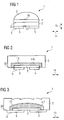
- FIG. 1 a modification of a semiconductor device 1 is shown.
- the semiconductor chip 2 is designed as a blue-emitting GaN-based light-emitting diode.
- the extent in the lateral direction 14, that is to say parallel to the chip underside 21, is preferably approximately 0.5 to 3 mm 2 and its thickness 50 to 300 ⁇ m.
- two electrical connection points 5 are attached on the chip bottom 21, two electrical connection points 5 are attached.
- the connection points 5 are in direct contact with the chip bottom side 21.
- the chip top side 22 is covered with an adhesive connection 4, which permanently connects the semiconductor chip 2 and the radiation-transmissive body 3 mechanically.
- the adhesive connection 4 is designed with a transparent, with respect to the emitted radiation from the semiconductor chip 2 aging resistant material, such as silicone or a silicone-epoxy hybrid material.
- the body 3 is designed to be spherical in shape, similar to a convex lens, and transparent to the radiation emitted by the semiconductor chip 2.
- the material of the body 3 is about thermoplastic. It is also possible to use materials from the group of silicones, epoxides, polycarbonates or hybrid materials. Likewise, the body 3 may be made of glasses. The material is preferred resistant to the environmental influences imposed by the specific application and resistant to aging with respect to the radiation to be received or emitted by the semiconductor chip 2.
- the extent in the lateral direction 14 of the semiconductor device 1 is equal to the extent in the lateral direction 14 of the semiconductor chip 2, that is electrical connection points 5 and adhesive connection 4 and body 3 are not in the lateral direction 14, so parallel to the chip bottom 21, on the semiconductor chip above. Also, the semiconductor device 1 is bounded by the semiconductor chip 2 facing away from the sides of the connection points 5 with respect to the mounting side 6. The mounting side 6 is aligned substantially parallel to the chip bottom 21.
- the semiconductor device 1 comprises a semiconductor chip 2, which is designed, for example, as a sensor for near-infrared radiation.
- a semiconductor chip 2 which is designed, for example, as a sensor for near-infrared radiation.
- On the chip bottom side 21 are two metallic connection points 5, which can be attached via surface mount technology, SMT short, to a non-subscribed, external support by means of about soldering or gluing. The connection points in turn limit the semiconductor device 1 in the direction of mounting side 6 downwards.
- a glued connection 4 configured with a transparent silicone is applied. This has a homogeneously distributed filter means 8 therein.
- the filter means 8 can be selected such that higher-frequency visible radiation components are filtered, so that the semiconductor chip 2 designed as a sensor is approximately only for near-infrared radiation is accessible.
- the semiconductor chip 2 may also be approximately a light-emitting diode which emits electromagnetic radiation during operation.
- a scattering or conversion agent 7 can be used.
- the semiconductor chip 2 has a square outline.
- the radiation-transmissive body 3 has a rectangular cross-section in plan view, is provided on the body bottom side 30 with a recess 13 and surrounds the semiconductor chip 2 laterally on only two opposite side surfaces, so that on the one hand the space requirement in the lateral direction 14 is minimized and on the other hand, the semiconductor chip 2 is well positioned in the recess 13 of the body.
- the recess 13 on the underside of the body 30 is dimensioned such that the semiconductor chip is in place and also sets the desired layer thickness of the adhesive joint 4.
- the recess 13 can be easily produced during the production of the body 3, for example as part of a casting process.
- the material for the radiation-transmissive body 3 As the material for the radiation-transmissive body 3, a transparent silicone is used.
- the upper side of the body 3 is shaped flat and designed scratch-resistant by the mechanical properties of the silicone used, which may optionally have a coating. This results in the semiconductor device 1 as a good Lambertian radiator.
- the electrical connection points 5 cover part of the chip underside 21 and, with the side facing the semiconductor chip 2, form a surface which is reflective for the radiation to be detected by the semiconductor chip 2 or emitted by the latter.
- the connection points 5 terminate flush with the semiconductor chip 2 in the lateral direction 14.
- the electrical connection points 5 can also be made of a transparent material, for example from the group of transparent conductive oxides, in short TCO, such as ITO. This is particularly advantageous if the external carrier to which the semiconductor device 1 is attached is also permeable to the relevant radiation.
- the semiconductor chip 2 is designed approximately as a laser or light emitting diode and emits light during operation.
- the connection points 5 protrude in the lateral direction 14 via the semiconductor chip 2, but not over the radiation-transmissive body 3.
- the semiconductor chip 2 facing side of the area-shaped connection points 5 closes in the vertical direction 15 flush with the body 3.
- the semiconductor chip 2 is surrounded by an adhesive connection 4.
- the adhesive connection 4 has an inhomogeneous thickness in such a way that the thickness is greater above the central region of the semiconductor chip 2 in the lateral direction 14 than at the edge regions.
- a conversion agent 7 is introduced in a constant over the entire adhesive bond 4 concentration.
- the inhomogeneous layer thickness of the adhesive joint 4 is automatically adjusted when gluing the semiconductor chip 2 in the body 3, since the a transparent aging-resistant material existing body 3 has a lens-like recess 13 on the body bottom 30, in which the semiconductor chip 2 is substantially.
- the top of the radiation-transmissive body 3 is formed as a Fresnel lens. The body 3 surrounds the semiconductor chip 2 on all side surfaces.
- the radiation-transmissive body 3 in this case is significantly larger in the lateral direction 14 than the semiconductor chip 2 located in a recess 13 on the underside of the body 30 in order to achieve a higher quality of the optical imaging.
- the electrical connection points 5 are again attached directly to the chip underside 21 and do not protrude beyond the semiconductor chip 2 in the lateral direction 14.
- the transparent adhesive connection 4 is configured with a silicone which has a refractive index of approximately 1.4.
- the convex lens-like shaped body 3 is formed with polycarbonate having a refractive index of about 1.6, so that the refractive index of the adhesive joint is smaller than that of the body.
- the beam path 16 of a photon emitted by the semiconductor chip 2 is shown schematically as a arrowed line.
- the photon is emitted at the edge of the chip top side 22 and runs at a small angle through the adhesive bond 4.
- a refraction of light takes place such that the photon is deflected away from the chip top side 22 in the vertical direction 15.
- photons can subsequently be better imaged by the radiation-transmissive body 3, since they impinge on the body-air interface closer to the optical axis of the body 3.
- the upper side of the radiation-transmissive body 3 is provided in places with a reflective layer 11.
- the reflective layer 11 is designed paraboloidally by means of the shaping of the body 3.
- the surface of the body 3 not covered by the reflective layer 11 has a lens-like shape.
- light emitted by the semiconductor chip 2, which is configured as an LED is either transmitted directly from the body, the radiation being emitted essentially in the direction of the arrow 18 via the lens-like structure of the body 3.
- Light which impinges on the reflective layer 11 is then also deflected by it substantially in the direction of arrow 18. In this way results in a semiconductor device 1, the light emitted effectively parallel to the chip top side 22.
- FIG. 5a shown construction are also other types as in FIG. 5b conceivable, for example, where the reflective layer 11 is mounted only in the laterally central region above the semiconductor chip 2, so that around the top of the radiation-transmissive body 3 remains free around. As a result, the radiation is radiated divergently rotationally symmetrically essentially laterally in the direction of arrow 18.
- the semiconductor chip can have, for example, corrugated outer surfaces which improve the light emission or light coupling from the semiconductor chip 2 or else for a mechanically more stable connection with adhesive connection 4 or radiation-transmissive body 3 to care. With such surface structuring and the body 3 may be provided.
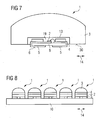
- a plurality of semiconductor chips 2 are housed in recesses 13 of the radiation-transmissive body 3.
- the semiconductor device 1 has two electrical connection points 5, which are SMT-contactable and the electrical contact to an external non-subscribed carrier, which may be designed approximately in the form of a metal core board has.
- electrical connections 12 are mounted, which are formed of a metal and how the connection points 5 are adhered to the contact surfaces of the semiconductor chip 2 with a conductive adhesive.
- the connections 12 have a smaller thickness than the two connection points 5.
- the body 3 is again formed lens-like. In this case, a large lens or for each semiconductor chip 2 a Sublinse be formed, depending on the requirements of the quality of the optical imaging.
- the adhesive bonds 4 may be mixed with various conversion means 7a, 7b, 7c.
- a semiconductor chip 2 is mounted on an intermediate carrier 9.
- the intermediate carrier 9 is essentially made of a thermally highly conductive ceramic.
- the electrical connection points 5 are guided from the side facing away from the semiconductor chip 2 to the semiconductor chip 2 side facing U-shaped and are SMT-contactable.
- the semiconductor chip 2 is electrically conductively bonded or soldered to the chip bottom 21 directly on one of the connection points 5 and connected to a further connection point 5 via a wire connection.
- the semiconductor chip 2 is seated in a recess 19 of the intermediate carrier 9, so that the connecting wire is not damaged when gluing or inserting the intermediate carrier 9 in the body 3.
- the electrical contacts on chip top 22 and chip bottom 21 are located, and semiconductor chips 2 can be used in flip-chip arrangement use. Also, a plurality of different types of semiconductor chips 2 emitting different colors may be mounted on the intermediate carrier 9 without great difficulty.
- the radiation-transmissive body 4 may be configured approximately in the form of a cylindrical lens.
- FIG. 8 are several modifications of semiconductor devices 1, constructed according to FIG. 1 , arranged on a thermally conductive support 10. Since the semiconductor chips 2 have no further bulk except for the body 3, and the space requirement in the lateral direction 13 is thus essentially limited to the lateral dimensions of the semiconductor chip 2, the semiconductor arrangements 1 can be packed in a highly dense manner. The waste heat produced during operation of the semiconductor chips 2 can be efficiently removed via the electrical connection points 5 and via the thermally conductive carrier 10. Since, as described, no further housing is used, the thermal contact of the semiconductor chips 2 to the carrier 10 is very well developed, in particular if the electrical connection points 5 are made flat and metallic. Via SMT, the individual semiconductor devices 1 can be mounted in a simple manner on the carrier 14 and there on accordingly manufactured, not drawn conductors are easily put on and soldered about.
- the semiconductor devices 1 For the high-density packing of the semiconductor devices 1, it is advantageous if they have approximately a square cross section in plan view. Just as convenient cross sections would be about circular, rectangular or hexagonal shapes.
- the body 3, which is embodied as lenses, can contain approximately different conversion means 7 or filter means 8, so that similar semiconductor chips 2 can be used and still different colors are radiated from the individual semiconductor arrangements 1, so that altogether a white light radiating illumination device or a different color radiating display device, for example, in conjunction with a liquid crystal mask can result.
- intermediate steps such as wire bonding become superfluous.
Landscapes
- Led Device Packages (AREA)
Applications Claiming Priority (2)
| Application Number | Priority Date | Filing Date | Title |
|---|---|---|---|
| DE102008025756.7A DE102008025756B4 (de) | 2008-05-29 | 2008-05-29 | Halbleiteranordnung |
| PCT/DE2009/000542 WO2009143795A1 (de) | 2008-05-29 | 2009-04-20 | Halbleiteranordnung |
Publications (2)
| Publication Number | Publication Date |
|---|---|
| EP2281315A1 EP2281315A1 (de) | 2011-02-09 |
| EP2281315B1 true EP2281315B1 (de) | 2018-10-17 |
Family
ID=41061228
Family Applications (1)
| Application Number | Title | Priority Date | Filing Date |
|---|---|---|---|
| EP09753511.6A Active EP2281315B1 (de) | 2008-05-29 | 2009-04-20 | Halbleiteranordnung |
Country Status (7)
Families Citing this family (22)
| Publication number | Priority date | Publication date | Assignee | Title |
|---|---|---|---|---|
| US9000461B2 (en) * | 2003-07-04 | 2015-04-07 | Epistar Corporation | Optoelectronic element and manufacturing method thereof |
| US10686106B2 (en) | 2003-07-04 | 2020-06-16 | Epistar Corporation | Optoelectronic element |
| US9142740B2 (en) | 2003-07-04 | 2015-09-22 | Epistar Corporation | Optoelectronic element and manufacturing method thereof |
| DE102009017946A1 (de) | 2009-04-17 | 2010-10-21 | Osram Opto Semiconductors Gmbh | Linse, optoelektronisches Bauelement aufweisend eine Linse und Verfahren zur Herstellung einer Linse |
| DE102009024425B4 (de) * | 2009-06-09 | 2011-11-17 | Diehl Aerospace Gmbh | Anschlusseinrichtung für eine lichtemittierende Diode und Beleuchtungseinheit |
| DE102010055265A1 (de) * | 2010-12-20 | 2012-06-21 | Osram Opto Semiconductors Gmbh | Optoelektronisches Halbleiterbauteil |
| CN102651446B (zh) * | 2011-02-25 | 2014-12-10 | 展晶科技(深圳)有限公司 | 发光二极管封装结构及光源装置 |
| DE102011102350A1 (de) | 2011-05-24 | 2012-11-29 | Osram Opto Semiconductors Gmbh | Optisches Element, optoelektronisches Bauelement und Verfahren zur Herstellung dieser |
| DE102011102590A1 (de) * | 2011-05-27 | 2012-11-29 | Osram Opto Semiconductors Gmbh | Verfahren zum Herstellen von Leuchtdioden-Bauelementen |
| KR102071088B1 (ko) | 2012-01-17 | 2020-01-29 | 루미리즈 홀딩 비.브이. | 큰 각도로 광을 방출하는 반도체 발광 디바이스 램프 |
| DE102012102122A1 (de) * | 2012-03-13 | 2013-09-19 | Osram Opto Semiconductors Gmbh | Flächenlichtquelle |
| DE102012102114B4 (de) * | 2012-03-13 | 2021-09-16 | OSRAM Opto Semiconductors Gesellschaft mit beschränkter Haftung | Strahlungsemittierendes Halbleiterbauteil, Beleuchtungsvorrichtung und Anzeigevorrichtung |
| US8889439B2 (en) * | 2012-08-24 | 2014-11-18 | Tsmc Solid State Lighting Ltd. | Method and apparatus for packaging phosphor-coated LEDs |
| WO2015011586A1 (en) * | 2013-07-26 | 2015-01-29 | Koninklijke Philips N.V. | Led dome with inner high index pillar |
| EP2854186A1 (en) * | 2013-09-26 | 2015-04-01 | Seoul Semiconductor Co., Ltd. | Light source module, fabrication method therefor, and backlight unit including the same |
| WO2015110927A1 (en) | 2014-01-23 | 2015-07-30 | Koninklijke Philips N.V. | Light emitting device with self-aligning preformed lens |
| JP2015165536A (ja) * | 2014-03-03 | 2015-09-17 | ウシオ電機株式会社 | 発光装置および発光モジュール |
| DE102014217986A1 (de) * | 2014-03-27 | 2015-10-01 | Tridonic Jennersdorf Gmbh | LED Modul mit integrierter Sekundäroptik |
| CN108604626B (zh) * | 2015-10-19 | 2022-02-18 | 亮锐控股有限公司 | 具有纹理化衬底的波长转换发光设备 |
| CN109148674B (zh) | 2017-06-28 | 2023-05-16 | 日亚化学工业株式会社 | 发光装置 |
| JP6899412B2 (ja) * | 2018-07-27 | 2021-07-07 | 住友化学株式会社 | Ledデバイスの製造方法 |
| WO2021144120A1 (de) * | 2020-01-13 | 2021-07-22 | Osram Opto Semiconductors Gmbh | Gehäuse, optoelektronisches halbleiterbauteil und herstellungsverfahren |
Family Cites Families (38)
| Publication number | Priority date | Publication date | Assignee | Title |
|---|---|---|---|---|
| US5216805A (en) * | 1990-12-12 | 1993-06-08 | Eastman Kodak Company | Method of manufacturing an optoelectronic device package |
| DE19625622A1 (de) | 1996-06-26 | 1998-01-02 | Siemens Ag | Lichtabstrahlendes Halbleiterbauelement mit Lumineszenzkonversionselement |
| EP2282354B1 (de) | 1996-06-26 | 2013-09-11 | OSRAM Opto Semiconductors GmbH | Licht abstrahlendes Halbleiterbauelement mit Lumineszenzkonversionselement |
| DE19638667C2 (de) | 1996-09-20 | 2001-05-17 | Osram Opto Semiconductors Gmbh | Mischfarbiges Licht abstrahlendes Halbleiterbauelement mit Lumineszenzkonversionselement |
| JP3696021B2 (ja) | 2000-01-20 | 2005-09-14 | 三洋電機株式会社 | 光照射装置 |
| DE10023353A1 (de) * | 2000-05-12 | 2001-11-29 | Osram Opto Semiconductors Gmbh | Optoelektronisches Bauelement und Verfahren zur Herstellung |
| US6345903B1 (en) | 2000-09-01 | 2002-02-12 | Citizen Electronics Co., Ltd. | Surface-mount type emitting diode and method of manufacturing same |
| US7053419B1 (en) * | 2000-09-12 | 2006-05-30 | Lumileds Lighting U.S., Llc | Light emitting diodes with improved light extraction efficiency |
| US7064355B2 (en) * | 2000-09-12 | 2006-06-20 | Lumileds Lighting U.S., Llc | Light emitting diodes with improved light extraction efficiency |
| TW474034B (en) | 2000-11-07 | 2002-01-21 | United Epitaxy Co Ltd | LED and the manufacturing method thereof |
| KR100638379B1 (ko) * | 2001-08-24 | 2006-10-26 | 쇼오트 아게 | 집적회로의 컨택 제조 및 하우징 공정 |
| US7160478B2 (en) | 2001-08-24 | 2007-01-09 | Schott Ag | Method for producing electronic componets |
| AU2003235453A1 (en) | 2002-05-28 | 2003-12-12 | Matsushita Electric Works, Ltd. | Light emitting element, light emitting device and surface emission illuminating device using it |
| JP2004128057A (ja) | 2002-09-30 | 2004-04-22 | Fuji Photo Film Co Ltd | 発光装置およびその製造方法 |
| CN1777999B (zh) | 2003-02-26 | 2010-05-26 | 美商克立股份有限公司 | 复合式白色光源及其制造方法 |
| JP4182784B2 (ja) * | 2003-03-14 | 2008-11-19 | 豊田合成株式会社 | 発光装置およびその製造方法 |
| US7061065B2 (en) | 2003-03-31 | 2006-06-13 | National Chung-Hsing University | Light emitting diode and method for producing the same |
| US7791274B2 (en) | 2004-01-07 | 2010-09-07 | Panasonic Corporation | LED lamp |
| US7361938B2 (en) | 2004-06-03 | 2008-04-22 | Philips Lumileds Lighting Company Llc | Luminescent ceramic for a light emitting device |
| US20050280016A1 (en) * | 2004-06-17 | 2005-12-22 | Mok Thye L | PCB-based surface mount LED device with silicone-based encapsulation structure |
| DE102004036157B4 (de) | 2004-07-26 | 2023-03-16 | OSRAM Opto Semiconductors Gesellschaft mit beschränkter Haftung | Elektromagnetische Strahlung emittierendes optoelektronisches Bauelement und Leuchtmodul |
| DE102004047640A1 (de) | 2004-09-30 | 2006-04-13 | Osram Opto Semiconductors Gmbh | Optoelektronisches Bauelement und Gehäuse für ein optoelektronisches Bauelement |
| US7419839B2 (en) | 2004-11-12 | 2008-09-02 | Philips Lumileds Lighting Company, Llc | Bonding an optical element to a light emitting device |
| KR20080006634A (ko) | 2005-04-28 | 2008-01-16 | 코닌클리즈케 필립스 일렉트로닉스 엔.브이. | 리세스 내에 배치된 led를 포함하는 광원 |
| DE102006037737A1 (de) | 2005-12-09 | 2007-06-14 | Osram Opto Semiconductors Gmbh | Optische Vorrichtung, optoelektronische Vorrichtung und Verfahren zur Herstellung einer optoelektronischen Vorrichtung |
| TW200735327A (en) | 2005-12-14 | 2007-09-16 | Koninkl Philips Electronics Nv | Collimation arrangement and illumination system and display device using the same |
| US7375379B2 (en) * | 2005-12-19 | 2008-05-20 | Philips Limileds Lighting Company, Llc | Light-emitting device |
| US7798678B2 (en) * | 2005-12-30 | 2010-09-21 | 3M Innovative Properties Company | LED with compound encapsulant lens |
| TWI303105B (en) * | 2006-01-11 | 2008-11-11 | Advanced Semiconductor Eng | Wafer level package for image sensor components and its fabricating method |
| JP2007242820A (ja) * | 2006-03-08 | 2007-09-20 | Asahi Kasei Corp | 発光デバイス及び発光デバイスモジュール |
| US7674641B2 (en) | 2006-04-12 | 2010-03-09 | Atomic Energy Council | Method for fabricating white-light-emitting flip-chip diode having silicon quantum dots |
| US7521862B2 (en) * | 2006-11-20 | 2009-04-21 | Philips Lumileds Lighting Co., Llc | Light emitting device including luminescent ceramic and light-scattering material |
| US7964888B2 (en) * | 2007-04-18 | 2011-06-21 | Cree, Inc. | Semiconductor light emitting device packages and methods |
| DE102007019776A1 (de) | 2007-04-26 | 2008-10-30 | Osram Opto Semiconductors Gmbh | Optoelektronisches Bauelement und Verfahren zur Herstellung einer Mehrzahl optoelektronischer Bauelemente |
| DE102007019775B4 (de) | 2007-04-26 | 2024-11-28 | OSRAM Opto Semiconductors Gesellschaft mit beschränkter Haftung | Optoelektronisches Bauelement |
| US7999283B2 (en) * | 2007-06-14 | 2011-08-16 | Cree, Inc. | Encapsulant with scatterer to tailor spatial emission pattern and color uniformity in light emitting diodes |
| KR101378418B1 (ko) * | 2007-11-01 | 2014-03-27 | 삼성전자주식회사 | 이미지센서 모듈 및 그 제조방법 |
| JP2010161321A (ja) * | 2009-01-09 | 2010-07-22 | Panasonic Corp | 光学デバイスおよびその製造方法 |
-
2008
- 2008-05-29 DE DE102008025756.7A patent/DE102008025756B4/de active Active
-
2009
- 2009-04-20 EP EP09753511.6A patent/EP2281315B1/de active Active
- 2009-04-20 KR KR1020107019817A patent/KR101634406B1/ko active Active
- 2009-04-20 US US12/995,181 patent/US8461616B2/en active Active
- 2009-04-20 JP JP2011510815A patent/JP2011521480A/ja active Pending
- 2009-04-20 CN CN200980109077XA patent/CN101971376B/zh active Active
- 2009-04-20 WO PCT/DE2009/000542 patent/WO2009143795A1/de active Application Filing
Non-Patent Citations (1)
| Title |
|---|
| None * |
Also Published As
| Publication number | Publication date |
|---|---|
| DE102008025756A1 (de) | 2009-12-03 |
| WO2009143795A1 (de) | 2009-12-03 |
| US20110266571A1 (en) | 2011-11-03 |
| CN101971376A (zh) | 2011-02-09 |
| KR101634406B1 (ko) | 2016-06-28 |
| JP2011521480A (ja) | 2011-07-21 |
| KR20110030417A (ko) | 2011-03-23 |
| US8461616B2 (en) | 2013-06-11 |
| EP2281315A1 (de) | 2011-02-09 |
| DE102008025756B4 (de) | 2023-02-23 |
| CN101971376B (zh) | 2013-01-02 |
Similar Documents
| Publication | Publication Date | Title |
|---|---|---|
| EP2281315B1 (de) | Halbleiteranordnung | |
| DE112019001502B4 (de) | Optoelektronisches bauelement und verfahren zur herstellung eines optoelektronischen bauelements | |
| EP2258000B1 (de) | Optoelektronisches halbleiterbauteil und verfahren zur herstellung eines optoelektronischen halbleiterbauteils | |
| EP2281316B1 (de) | Optoelektronisches halbleiterbauteil | |
| DE102008038748B4 (de) | Oberflächenmontierbares, optoelektronisches Halbleiterbauteil | |
| WO2020169524A1 (de) | Optoelektronisches halbleiterbauteil und herstellungsverfahren für optoelektronische halbleiterbauteile | |
| DE102010055265A1 (de) | Optoelektronisches Halbleiterbauteil | |
| EP2901479B1 (de) | Optoelektronisches bauelement | |
| DE102011080458A1 (de) | Optoelektronische anordnung und verfahren zur herstellung einer optoelektronischen anordnung | |
| DE102011087886A1 (de) | Halbleiterleuchte | |
| EP2583319A1 (de) | Optoelektronisches bauteil | |
| WO2013167399A1 (de) | Optoelektronisches bauelement und verfahren zum herstellen eines optoelektronischen bauelements | |
| WO2013010765A1 (de) | Optoelektronisches bauelement und verfahren zur herstellung eines optoelektronischen bauelements | |
| DE102013207308A1 (de) | Verfahren zum Herstellen einer optoelektronischen Baugruppe und optoelektronische Baugruppe | |
| WO2013139735A1 (de) | Optoelektronisches halbleiterbauteil und verfahren zur herstellung eines solchen | |
| WO2020173830A1 (de) | Optoelektronisches halbleiterbauteil und verfahren zur herstellung eines optoelektronischen halbleiterbauteils | |
| WO2013110540A1 (de) | Leuchte und verfahren zur herstellung einer leuchte | |
| DE112014003593B4 (de) | Anordnung mit mindestens einem optoelektronischen Halbleiterchip | |
| WO2009143794A1 (de) | Optoelektronisches modul und optoelektronische anordnung | |
| DE102015111910A1 (de) | Optoelektronisches Bauelement, Verbund von optoelektronischen Bauelementen und Verfahren zur Herstellung eines optoelektronischen Bauelements | |
| DE202022104777U1 (de) | Laser-Phosphor-integrierte Lichtquelle | |
| WO2009103285A1 (de) | Optoelektronisches bauteil | |
| DE102011087614A1 (de) | Optoelektronische Anordnung | |
| WO2012013435A1 (de) | Licht emittierendes halbleiterbauelement und verfahren zur herstellung eines licht emittierenden halbleiterbauelements | |
| WO2021239542A1 (de) | Optoelektronisches halbleiterbauteil und verfahren zur herstellung von optoelektronischen halbleiterbauteilen |
Legal Events
| Date | Code | Title | Description |
|---|---|---|---|
| PUAI | Public reference made under article 153(3) epc to a published international application that has entered the european phase |
Free format text: ORIGINAL CODE: 0009012 |
|
| 17P | Request for examination filed |
Effective date: 20100809 |
|
| AK | Designated contracting states |
Kind code of ref document: A1 Designated state(s): AT BE BG CH CY CZ DE DK EE ES FI FR GB GR HR HU IE IS IT LI LT LU LV MC MK MT NL NO PL PT RO SE SI SK TR |
|
| AX | Request for extension of the european patent |
Extension state: AL BA RS |
|
| DAX | Request for extension of the european patent (deleted) | ||
| STAA | Information on the status of an ep patent application or granted ep patent |
Free format text: STATUS: EXAMINATION IS IN PROGRESS |
|
| 17Q | First examination report despatched |
Effective date: 20180228 |
|
| REG | Reference to a national code |
Ref country code: DE Ref legal event code: R079 Ref document number: 502009015377 Country of ref document: DE Free format text: PREVIOUS MAIN CLASS: H01L0033000000 Ipc: H01L0033580000 |
|
| GRAP | Despatch of communication of intention to grant a patent |
Free format text: ORIGINAL CODE: EPIDOSNIGR1 |
|
| STAA | Information on the status of an ep patent application or granted ep patent |
Free format text: STATUS: GRANT OF PATENT IS INTENDED |
|
| RIC1 | Information provided on ipc code assigned before grant |
Ipc: H01L 33/58 20100101AFI20180626BHEP Ipc: H01L 25/075 20060101ALN20180626BHEP Ipc: H01L 33/60 20100101ALN20180626BHEP Ipc: H01L 33/54 20100101ALI20180626BHEP Ipc: H01L 33/38 20100101ALN20180626BHEP Ipc: H01L 25/04 20060101ALN20180626BHEP Ipc: H01L 33/62 20100101ALN20180626BHEP |
|
| INTG | Intention to grant announced |
Effective date: 20180719 |
|
| GRAS | Grant fee paid |
Free format text: ORIGINAL CODE: EPIDOSNIGR3 |
|
| GRAA | (expected) grant |
Free format text: ORIGINAL CODE: 0009210 |
|
| STAA | Information on the status of an ep patent application or granted ep patent |
Free format text: STATUS: THE PATENT HAS BEEN GRANTED |
|
| AK | Designated contracting states |
Kind code of ref document: B1 Designated state(s): AT BE BG CH CY CZ DE DK EE ES FI FR GB GR HR HU IE IS IT LI LT LU LV MC MK MT NL NO PL PT RO SE SI SK TR |
|
| REG | Reference to a national code |
Ref country code: GB Ref legal event code: FG4D Free format text: NOT ENGLISH |
|
| REG | Reference to a national code |
Ref country code: CH Ref legal event code: EP |
|
| REG | Reference to a national code |
Ref country code: IE Ref legal event code: FG4D Free format text: LANGUAGE OF EP DOCUMENT: GERMAN |
|
| REG | Reference to a national code |
Ref country code: DE Ref legal event code: R096 Ref document number: 502009015377 Country of ref document: DE Ref country code: AT Ref legal event code: REF Ref document number: 1055009 Country of ref document: AT Kind code of ref document: T Effective date: 20181115 |
|
| REG | Reference to a national code |
Ref country code: NL Ref legal event code: MP Effective date: 20181017 |
|
| REG | Reference to a national code |
Ref country code: LT Ref legal event code: MG4D |
|
| PG25 | Lapsed in a contracting state [announced via postgrant information from national office to epo] |
Ref country code: NL Free format text: LAPSE BECAUSE OF FAILURE TO SUBMIT A TRANSLATION OF THE DESCRIPTION OR TO PAY THE FEE WITHIN THE PRESCRIBED TIME-LIMIT Effective date: 20181017 |
|
| PG25 | Lapsed in a contracting state [announced via postgrant information from national office to epo] |
Ref country code: LV Free format text: LAPSE BECAUSE OF FAILURE TO SUBMIT A TRANSLATION OF THE DESCRIPTION OR TO PAY THE FEE WITHIN THE PRESCRIBED TIME-LIMIT Effective date: 20181017 Ref country code: ES Free format text: LAPSE BECAUSE OF FAILURE TO SUBMIT A TRANSLATION OF THE DESCRIPTION OR TO PAY THE FEE WITHIN THE PRESCRIBED TIME-LIMIT Effective date: 20181017 Ref country code: NO Free format text: LAPSE BECAUSE OF FAILURE TO SUBMIT A TRANSLATION OF THE DESCRIPTION OR TO PAY THE FEE WITHIN THE PRESCRIBED TIME-LIMIT Effective date: 20190117 Ref country code: IS Free format text: LAPSE BECAUSE OF FAILURE TO SUBMIT A TRANSLATION OF THE DESCRIPTION OR TO PAY THE FEE WITHIN THE PRESCRIBED TIME-LIMIT Effective date: 20190217 Ref country code: FI Free format text: LAPSE BECAUSE OF FAILURE TO SUBMIT A TRANSLATION OF THE DESCRIPTION OR TO PAY THE FEE WITHIN THE PRESCRIBED TIME-LIMIT Effective date: 20181017 Ref country code: LT Free format text: LAPSE BECAUSE OF FAILURE TO SUBMIT A TRANSLATION OF THE DESCRIPTION OR TO PAY THE FEE WITHIN THE PRESCRIBED TIME-LIMIT Effective date: 20181017 Ref country code: PL Free format text: LAPSE BECAUSE OF FAILURE TO SUBMIT A TRANSLATION OF THE DESCRIPTION OR TO PAY THE FEE WITHIN THE PRESCRIBED TIME-LIMIT Effective date: 20181017 Ref country code: BG Free format text: LAPSE BECAUSE OF FAILURE TO SUBMIT A TRANSLATION OF THE DESCRIPTION OR TO PAY THE FEE WITHIN THE PRESCRIBED TIME-LIMIT Effective date: 20190117 Ref country code: HR Free format text: LAPSE BECAUSE OF FAILURE TO SUBMIT A TRANSLATION OF THE DESCRIPTION OR TO PAY THE FEE WITHIN THE PRESCRIBED TIME-LIMIT Effective date: 20181017 |
|
| PG25 | Lapsed in a contracting state [announced via postgrant information from national office to epo] |
Ref country code: GR Free format text: LAPSE BECAUSE OF FAILURE TO SUBMIT A TRANSLATION OF THE DESCRIPTION OR TO PAY THE FEE WITHIN THE PRESCRIBED TIME-LIMIT Effective date: 20190118 Ref country code: SE Free format text: LAPSE BECAUSE OF FAILURE TO SUBMIT A TRANSLATION OF THE DESCRIPTION OR TO PAY THE FEE WITHIN THE PRESCRIBED TIME-LIMIT Effective date: 20181017 Ref country code: PT Free format text: LAPSE BECAUSE OF FAILURE TO SUBMIT A TRANSLATION OF THE DESCRIPTION OR TO PAY THE FEE WITHIN THE PRESCRIBED TIME-LIMIT Effective date: 20190217 |
|
| REG | Reference to a national code |
Ref country code: DE Ref legal event code: R097 Ref document number: 502009015377 Country of ref document: DE |
|
| PG25 | Lapsed in a contracting state [announced via postgrant information from national office to epo] |
Ref country code: DK Free format text: LAPSE BECAUSE OF FAILURE TO SUBMIT A TRANSLATION OF THE DESCRIPTION OR TO PAY THE FEE WITHIN THE PRESCRIBED TIME-LIMIT Effective date: 20181017 Ref country code: IT Free format text: LAPSE BECAUSE OF FAILURE TO SUBMIT A TRANSLATION OF THE DESCRIPTION OR TO PAY THE FEE WITHIN THE PRESCRIBED TIME-LIMIT Effective date: 20181017 Ref country code: CZ Free format text: LAPSE BECAUSE OF FAILURE TO SUBMIT A TRANSLATION OF THE DESCRIPTION OR TO PAY THE FEE WITHIN THE PRESCRIBED TIME-LIMIT Effective date: 20181017 |
|
| PLBE | No opposition filed within time limit |
Free format text: ORIGINAL CODE: 0009261 |
|
| STAA | Information on the status of an ep patent application or granted ep patent |
Free format text: STATUS: NO OPPOSITION FILED WITHIN TIME LIMIT |
|
| PG25 | Lapsed in a contracting state [announced via postgrant information from national office to epo] |
Ref country code: RO Free format text: LAPSE BECAUSE OF FAILURE TO SUBMIT A TRANSLATION OF THE DESCRIPTION OR TO PAY THE FEE WITHIN THE PRESCRIBED TIME-LIMIT Effective date: 20181017 Ref country code: EE Free format text: LAPSE BECAUSE OF FAILURE TO SUBMIT A TRANSLATION OF THE DESCRIPTION OR TO PAY THE FEE WITHIN THE PRESCRIBED TIME-LIMIT Effective date: 20181017 Ref country code: SK Free format text: LAPSE BECAUSE OF FAILURE TO SUBMIT A TRANSLATION OF THE DESCRIPTION OR TO PAY THE FEE WITHIN THE PRESCRIBED TIME-LIMIT Effective date: 20181017 |
|
| RAP2 | Party data changed (patent owner data changed or rights of a patent transferred) |
Owner name: OSRAM OPTO SEMICONDUCTORS GMBH |
|
| 26N | No opposition filed |
Effective date: 20190718 |
|
| PG25 | Lapsed in a contracting state [announced via postgrant information from national office to epo] |
Ref country code: SI Free format text: LAPSE BECAUSE OF FAILURE TO SUBMIT A TRANSLATION OF THE DESCRIPTION OR TO PAY THE FEE WITHIN THE PRESCRIBED TIME-LIMIT Effective date: 20181017 |
|
| REG | Reference to a national code |
Ref country code: CH Ref legal event code: PL |
|
| REG | Reference to a national code |
Ref country code: BE Ref legal event code: MM Effective date: 20190430 |
|
| GBPC | Gb: european patent ceased through non-payment of renewal fee |
Effective date: 20190420 |
|
| PG25 | Lapsed in a contracting state [announced via postgrant information from national office to epo] |
Ref country code: LU Free format text: LAPSE BECAUSE OF NON-PAYMENT OF DUE FEES Effective date: 20190420 Ref country code: MC Free format text: LAPSE BECAUSE OF FAILURE TO SUBMIT A TRANSLATION OF THE DESCRIPTION OR TO PAY THE FEE WITHIN THE PRESCRIBED TIME-LIMIT Effective date: 20181017 |
|
| PG25 | Lapsed in a contracting state [announced via postgrant information from national office to epo] |
Ref country code: GB Free format text: LAPSE BECAUSE OF NON-PAYMENT OF DUE FEES Effective date: 20190420 Ref country code: CH Free format text: LAPSE BECAUSE OF NON-PAYMENT OF DUE FEES Effective date: 20190430 Ref country code: LI Free format text: LAPSE BECAUSE OF NON-PAYMENT OF DUE FEES Effective date: 20190430 |
|
| PG25 | Lapsed in a contracting state [announced via postgrant information from national office to epo] |
Ref country code: FR Free format text: LAPSE BECAUSE OF NON-PAYMENT OF DUE FEES Effective date: 20190430 Ref country code: BE Free format text: LAPSE BECAUSE OF NON-PAYMENT OF DUE FEES Effective date: 20190430 |
|
| PG25 | Lapsed in a contracting state [announced via postgrant information from national office to epo] |
Ref country code: TR Free format text: LAPSE BECAUSE OF FAILURE TO SUBMIT A TRANSLATION OF THE DESCRIPTION OR TO PAY THE FEE WITHIN THE PRESCRIBED TIME-LIMIT Effective date: 20181017 |
|
| PG25 | Lapsed in a contracting state [announced via postgrant information from national office to epo] |
Ref country code: IE Free format text: LAPSE BECAUSE OF NON-PAYMENT OF DUE FEES Effective date: 20190420 |
|
| REG | Reference to a national code |
Ref country code: AT Ref legal event code: MM01 Ref document number: 1055009 Country of ref document: AT Kind code of ref document: T Effective date: 20190420 |
|
| PG25 | Lapsed in a contracting state [announced via postgrant information from national office to epo] |
Ref country code: AT Free format text: LAPSE BECAUSE OF NON-PAYMENT OF DUE FEES Effective date: 20190420 |
|
| PG25 | Lapsed in a contracting state [announced via postgrant information from national office to epo] |
Ref country code: CY Free format text: LAPSE BECAUSE OF FAILURE TO SUBMIT A TRANSLATION OF THE DESCRIPTION OR TO PAY THE FEE WITHIN THE PRESCRIBED TIME-LIMIT Effective date: 20181017 |
|
| PG25 | Lapsed in a contracting state [announced via postgrant information from national office to epo] |
Ref country code: HU Free format text: LAPSE BECAUSE OF FAILURE TO SUBMIT A TRANSLATION OF THE DESCRIPTION OR TO PAY THE FEE WITHIN THE PRESCRIBED TIME-LIMIT; INVALID AB INITIO Effective date: 20090420 Ref country code: MT Free format text: LAPSE BECAUSE OF FAILURE TO SUBMIT A TRANSLATION OF THE DESCRIPTION OR TO PAY THE FEE WITHIN THE PRESCRIBED TIME-LIMIT Effective date: 20181017 |
|
| PG25 | Lapsed in a contracting state [announced via postgrant information from national office to epo] |
Ref country code: MK Free format text: LAPSE BECAUSE OF FAILURE TO SUBMIT A TRANSLATION OF THE DESCRIPTION OR TO PAY THE FEE WITHIN THE PRESCRIBED TIME-LIMIT Effective date: 20181017 |
|
| P01 | Opt-out of the competence of the unified patent court (upc) registered |
Effective date: 20230825 |
|
| REG | Reference to a national code |
Ref country code: DE Ref legal event code: R079 Ref document number: 502009015377 Country of ref document: DE Free format text: PREVIOUS MAIN CLASS: H01L0033580000 Ipc: H10H0020855000 |
|
| PGFP | Annual fee paid to national office [announced via postgrant information from national office to epo] |
Ref country code: DE Payment date: 20250422 Year of fee payment: 17 |