EP2280255A1 - Quantumpunktbasierte Strahlungsquelle und radiometrischer Kalibrator damit - Google Patents
Quantumpunktbasierte Strahlungsquelle und radiometrischer Kalibrator damit Download PDFInfo
- Publication number
- EP2280255A1 EP2280255A1 EP10164071A EP10164071A EP2280255A1 EP 2280255 A1 EP2280255 A1 EP 2280255A1 EP 10164071 A EP10164071 A EP 10164071A EP 10164071 A EP10164071 A EP 10164071A EP 2280255 A1 EP2280255 A1 EP 2280255A1
- Authority
- EP
- European Patent Office
- Prior art keywords
- radiation
- quantum dots
- radiation source
- housing
- source
- Prior art date
- Legal status (The legal status is an assumption and is not a legal conclusion. Google has not performed a legal analysis and makes no representation as to the accuracy of the status listed.)
- Granted
Links
- 239000002096 quantum dot Substances 0.000 title claims abstract description 182
- 230000005855 radiation Effects 0.000 title claims abstract description 181
- 230000005284 excitation Effects 0.000 claims abstract description 19
- 230000003287 optical effect Effects 0.000 claims abstract description 6
- 238000004891 communication Methods 0.000 claims abstract description 5
- 238000000034 method Methods 0.000 claims description 19
- 238000001228 spectrum Methods 0.000 claims description 19
- 239000000203 mixture Substances 0.000 claims description 15
- 239000000463 material Substances 0.000 claims description 13
- 239000000126 substance Substances 0.000 claims description 9
- 239000000758 substrate Substances 0.000 claims description 9
- UHYPYGJEEGLRJD-UHFFFAOYSA-N cadmium(2+);selenium(2-) Chemical compound [Se-2].[Cd+2] UHYPYGJEEGLRJD-UHFFFAOYSA-N 0.000 claims description 8
- 230000004907 flux Effects 0.000 claims description 5
- 229910004613 CdTe Inorganic materials 0.000 claims description 3
- 229910004262 HgTe Inorganic materials 0.000 claims description 2
- 229910002665 PbTe Inorganic materials 0.000 claims description 2
- WPYVAWXEWQSOGY-UHFFFAOYSA-N indium antimonide Chemical compound [Sb]#[In] WPYVAWXEWQSOGY-UHFFFAOYSA-N 0.000 claims description 2
- OCGWQDWYSQAFTO-UHFFFAOYSA-N tellanylidenelead Chemical compound [Pb]=[Te] OCGWQDWYSQAFTO-UHFFFAOYSA-N 0.000 claims description 2
- 230000001419 dependent effect Effects 0.000 claims 1
- 238000000576 coating method Methods 0.000 description 8
- 239000011248 coating agent Substances 0.000 description 7
- 238000000295 emission spectrum Methods 0.000 description 6
- 239000011159 matrix material Substances 0.000 description 6
- 239000002131 composite material Substances 0.000 description 4
- 239000002159 nanocrystal Substances 0.000 description 4
- 229920000642 polymer Polymers 0.000 description 4
- 238000010438 heat treatment Methods 0.000 description 3
- 238000012986 modification Methods 0.000 description 3
- 230000004048 modification Effects 0.000 description 3
- 239000000178 monomer Substances 0.000 description 3
- 230000008569 process Effects 0.000 description 3
- 238000000862 absorption spectrum Methods 0.000 description 2
- 230000015572 biosynthetic process Effects 0.000 description 2
- 239000013590 bulk material Substances 0.000 description 2
- 238000009826 distribution Methods 0.000 description 2
- 230000000694 effects Effects 0.000 description 2
- 238000004020 luminiscence type Methods 0.000 description 2
- 239000002243 precursor Substances 0.000 description 2
- 238000002310 reflectometry Methods 0.000 description 2
- 230000003595 spectral effect Effects 0.000 description 2
- 238000003786 synthesis reaction Methods 0.000 description 2
- -1 HgSe Inorganic materials 0.000 description 1
- 101000878457 Macrocallista nimbosa FMRFamide Proteins 0.000 description 1
- 241000287181 Sturnus vulgaris Species 0.000 description 1
- 238000000137 annealing Methods 0.000 description 1
- 238000013459 approach Methods 0.000 description 1
- 230000008859 change Effects 0.000 description 1
- 238000010276 construction Methods 0.000 description 1
- 238000011109 contamination Methods 0.000 description 1
- 239000013078 crystal Substances 0.000 description 1
- 238000000151 deposition Methods 0.000 description 1
- 238000005516 engineering process Methods 0.000 description 1
- 238000011066 ex-situ storage Methods 0.000 description 1
- 238000001914 filtration Methods 0.000 description 1
- 230000017525 heat dissipation Effects 0.000 description 1
- 238000005286 illumination Methods 0.000 description 1
- LQBJWKCYZGMFEV-UHFFFAOYSA-N lead tin Chemical compound [Sn].[Pb] LQBJWKCYZGMFEV-UHFFFAOYSA-N 0.000 description 1
- 238000004519 manufacturing process Methods 0.000 description 1
- 238000005297 material degradation process Methods 0.000 description 1
- 238000002156 mixing Methods 0.000 description 1
- 230000006911 nucleation Effects 0.000 description 1
- 238000010899 nucleation Methods 0.000 description 1
- 239000013307 optical fiber Substances 0.000 description 1
- 239000012429 reaction media Substances 0.000 description 1
- 230000008707 rearrangement Effects 0.000 description 1
- SBIBMFFZSBJNJF-UHFFFAOYSA-N selenium;zinc Chemical compound [Se]=[Zn] SBIBMFFZSBJNJF-UHFFFAOYSA-N 0.000 description 1
- 239000004065 semiconductor Substances 0.000 description 1
- 230000035945 sensitivity Effects 0.000 description 1
- 239000002904 solvent Substances 0.000 description 1
- 239000004094 surface-active agent Substances 0.000 description 1
Images


Classifications
-
- G—PHYSICS
- G01—MEASURING; TESTING
- G01J—MEASUREMENT OF INTENSITY, VELOCITY, SPECTRAL CONTENT, POLARISATION, PHASE OR PULSE CHARACTERISTICS OF INFRARED, VISIBLE OR ULTRAVIOLET LIGHT; COLORIMETRY; RADIATION PYROMETRY
- G01J1/00—Photometry, e.g. photographic exposure meter
- G01J1/02—Details
- G01J1/08—Arrangements of light sources specially adapted for photometry standard sources, also using luminescent or radioactive material
-
- G—PHYSICS
- G01—MEASURING; TESTING
- G01J—MEASUREMENT OF INTENSITY, VELOCITY, SPECTRAL CONTENT, POLARISATION, PHASE OR PULSE CHARACTERISTICS OF INFRARED, VISIBLE OR ULTRAVIOLET LIGHT; COLORIMETRY; RADIATION PYROMETRY
- G01J1/00—Photometry, e.g. photographic exposure meter
- G01J1/58—Photometry, e.g. photographic exposure meter using luminescence generated by light
-
- G—PHYSICS
- G01—MEASURING; TESTING
- G01J—MEASUREMENT OF INTENSITY, VELOCITY, SPECTRAL CONTENT, POLARISATION, PHASE OR PULSE CHARACTERISTICS OF INFRARED, VISIBLE OR ULTRAVIOLET LIGHT; COLORIMETRY; RADIATION PYROMETRY
- G01J5/00—Radiation pyrometry, e.g. infrared or optical thermometry
- G01J5/52—Radiation pyrometry, e.g. infrared or optical thermometry using comparison with reference sources, e.g. disappearing-filament pyrometer
- G01J5/53—Reference sources, e.g. standard lamps; Black bodies
-
- G—PHYSICS
- G01—MEASURING; TESTING
- G01N—INVESTIGATING OR ANALYSING MATERIALS BY DETERMINING THEIR CHEMICAL OR PHYSICAL PROPERTIES
- G01N21/00—Investigating or analysing materials by the use of optical means, i.e. using sub-millimetre waves, infrared, visible or ultraviolet light
- G01N21/17—Systems in which incident light is modified in accordance with the properties of the material investigated
- G01N21/25—Colour; Spectral properties, i.e. comparison of effect of material on the light at two or more different wavelengths or wavelength bands
- G01N21/255—Details, e.g. use of specially adapted sources, lighting or optical systems
-
- G—PHYSICS
- G01—MEASURING; TESTING
- G01N—INVESTIGATING OR ANALYSING MATERIALS BY DETERMINING THEIR CHEMICAL OR PHYSICAL PROPERTIES
- G01N21/00—Investigating or analysing materials by the use of optical means, i.e. using sub-millimetre waves, infrared, visible or ultraviolet light
- G01N21/17—Systems in which incident light is modified in accordance with the properties of the material investigated
- G01N21/25—Colour; Spectral properties, i.e. comparison of effect of material on the light at two or more different wavelengths or wavelength bands
- G01N21/27—Colour; Spectral properties, i.e. comparison of effect of material on the light at two or more different wavelengths or wavelength bands using photo-electric detection ; circuits for computing concentration
- G01N21/274—Calibration, base line adjustment, drift correction
-
- G—PHYSICS
- G01—MEASURING; TESTING
- G01J—MEASUREMENT OF INTENSITY, VELOCITY, SPECTRAL CONTENT, POLARISATION, PHASE OR PULSE CHARACTERISTICS OF INFRARED, VISIBLE OR ULTRAVIOLET LIGHT; COLORIMETRY; RADIATION PYROMETRY
- G01J1/00—Photometry, e.g. photographic exposure meter
- G01J1/02—Details
- G01J1/04—Optical or mechanical part supplementary adjustable parts
- G01J2001/0481—Preset integrating sphere or cavity
Definitions
- This disclosure pertains to quantum dots, and particularly to a quantum dot based radiation source, a radiometric calibrator using the quantum dot radiation source, and a method of calibrating a detector using the quantum dot based radiation source.
- Radiometric calibration is utilized to associate or link intensities measured by a sensor or detector (such as intensities measured by each pixel of a charge coupled device (CCD)) to a physical parameter.
- radiometric calibration allows comparison of wavelength spectral intensities from different radiation sources.
- Radiometric calibration may be needed as the photon flux distribution in the unprocessed detected wavelength spectrum can be different from the photons flux distribution in the wavelength spectrum that is emitted by the observed object or source of radiation. This can be due to the fact that the photons detected by the sensor or detector (e.g., CCD) traversed several filters, such as the atmosphere, which can act as filter in certain regions of the wavelength spectrum, as well as filtering devices in the detector.
- radiometric calibration may be needed due to the fact that the detector or sensor quantum efficiency is not flat across the detected wavelength spectrum.
- radiometric calibration may be needed by electro-optical instruments, such as electro-optical instruments used for remote sensing (e.g., space-based remote sensing instruments) to establish a relationship or link between the signal output by the instrument and the photon flux emitted by the object under study.
- electro-optical instruments such as electro-optical instruments used for remote sensing (e.g., space-based remote sensing instruments) to establish a relationship or link between the signal output by the instrument and the photon flux emitted by the object under study.
- radiometric calibration may be used to know how a pixel's "dark number" correlates to a fixed unit of illumination (W/cm 2 or photons/cm 2 -s).
- radiometric calibration can also provide meaningful comparison of different observed phenomena.
- LEDs light emitting diodes
- LEDs are generally more stable than filament based lamps.
- LEDs emit in narrow wavelength ranges and, as a result, can only cover a limited portion of the radiation spectrum.
- Other light sources used for radiometric calibration include the use of solar diffusers which usually require checks by other sources (ground images). However, the solar diffusers degrade over life due to material degradation, contamination or mechanical problems.
- the use of solar diffusers for calibration include calibrating ex-situ by looking at features on the ground that have a known reflectivity. For example, the instrument stares at a patch of snow on the earth.
- these methods have limitations, since the reflectivity of the material (e.g., snow on the ground surface) can change over time and thus affect the reflected spectrum.
- An embodiment of this disclosure provides a quantum dot based radiation source comprising a housing having a wall defining a cavity therein, a plurality of quantum dots disposed on an inner surface of the wall of the housing; and a radiation excitation source in optical communication with the housing and configured to output radiation to excite the plurality of quantum dots to emit radiation in a desired wavelength range.
- the quantum dot based radiation source includes a housing having a wall defining a cavity therein, a plurality of quantum dots disposed on an inner surface of the wall of the housing, and a radiation excitation source in optical communication with the housing and configured to output radiation to excite the plurality of quantum dots to emit radiation in a desired wavelength range.
- Yet another embodiment of this disclosure provides a method of calibrating a radiation detector.
- the method comprises exciting a plurality of quantum dots with a first radiation so that the quantum dots emit a second radiation in a desired wavelength range, the quantum dots being disposed on an inner surface of a wall of a housing defining a cavity therein; outputting the second radiation through an output port in the housing; and guiding the second radiation towards the radiation detector to calibrate the detector.
- FIG. 1 is a schematic representation of a quantum dot based radiation source, according to an embodiment
- FIG. 2 shows an example of the radiation spectrum output by a UV LED
- FIG. 3 depicts a theoretical broad range absorption spectrum of the quantum dots along with the narrow resonant emission characteristic of quantum dots
- FIG. 4 shows a wavelength emission range of various quantum dot materials depending upon the size of the quantum dots
- FIG. 5 is a plot of luminescence peaks of CdSe quantum dots as a function of wavelength for various sizes of the CdSe quantum dots;
- FIG. 6 is a plot showing the relationship between the wavelength of emitted radiation peak and the size (e.g., diameter) of the quantum dots;
- FIG. 7 shows a composite spectrum obtained by using various types of quantum dots, according to one embodiment
- FIG. 8 shows emission spectra of various quantum dot types when excited with ultraviolet radiation, according to one embodiment
- FIG. 9 shows emission spectra of various quantum dot types when excited with ultraviolet radiation, according to another embodiment.
- FIG. 10 shows a calibration system or calibrator using the quantum dot based radiation source shown in FIG. 1 , for calibrating a detector, according to one embodiment.
- FIG. 1 is a schematic representation of a quantum dot based radiation source, according to an embodiment.
- Quantum dot based radiation source 10 includes integrating sphere 12.
- Integrating sphere 12 includes housing 11 having wall 13 forming hollow cavity 14.
- Inner surface 15 of wall 13 of integrating sphere 12 is coated with radiation diffusing reflective coating, such as SPECTRALONTM or SPECTRAFLECTTM coatings manufactured by Labsphere, Inc.
- the shape of cavity 14 is commonly spherical, hence the name of "integrating sphere".
- housing 11 defining cavity 14 can have other shapes such as dodecahedron, icosidodecahedron, icosahedron, or the like.
- an integrating sphere is used for its diffusing effect.
- an integrating sphere may be seen as a diffuser which preserves power but destroys spatial information.
- portion 15A of inner surface 15 of wall 13 (e.g., about one half of inner surface 15 or one hemisphere) is coated with the radiation reflective coating while another portion 15B of inner surface 15 of wall 13 (e.g., the other half of total inner surface 15 or opposite hemisphere) is not coated with the radiation reflective coating.
- a plurality of panels 16 coated with quantum dots 18 are provided on portion 15B of inner surface 15 of wall 13.
- Quantum dot based radiation source 10 further includes excitation radiation source 20.
- Excitation radiation source 20 is used to excite quantum dots 18 to emit a photon (one or more photons).
- excitation radiation source 20 comprises a plurality of light emitting diodes (LEDs) 22.
- LEDs 22 any other type of source can be used.
- Excitation radiation source 20 e.g., LEDs 22
- housing 11 In one embodiment, LEDs 22 can be disposed spaced apart around the "equator" of integrating sphere 22. However, as it can be appreciated LEDs 22 can be arranged in housing 11 of integrating sphere 22 in any desired location and/or configuration. For example, LEDs 22 can be provided at one spot of housing 11.
- LEDs 22 can be selected according to their radiation power output and/or their spectral output.
- LEDs 22 can be selected from LEDs that emit in the ultraviolet (UV) spectrum such as UV LEDs made by Phoseon Technology Corporation.
- the excitation radiation source 20 e.g., LEDs 22
- optical waveguides e.g. optical fibers
- FIG. 2 shows an example of the spectrum of radiation output by a UV LED.
- the UV LED can provide a stable intensity output over the operation lifetime of the UV LED which can be 15000 hours or more.
- LEDs 22 can be selected to emit in a same range of wavelengths or different ranges of wavelengths. For example, in one embodiment, some of LEDs 22 can be selected to emit in one ultraviolet wavelength range while other LEDs 22 can be selected to emit in another ultraviolet wavelength range or in the visible wavelength range.
- excitation radiation source 20 e.g., light emitted by LEDs 22
- the reflected excitation radiation is absorbed by quantum dots 18 disposed on substrate panels 16.
- the quantum dots in turn emit radiation at a wavelength equal or longer than the wavelength of excitation radiation source 20 (e.g., LEDs 22).
- excitation radiation source 20 has a wavelength shorter than or equal to the wavelength emitted by quantum dots 18.
- the radiation emitted by the quantum dots also undergoes multiple reflections by the radiation reflective coating within cavity 14.
- Exit or output port 17 is provided in wall 13 to allow radiation that is emitted by the quantum dots and reflected and diffused by the coating on inner surface 15 to exit through exit port 17.
- Tube 19 may be provided to guide the light output through output port 17.
- quantum dots 18 can reemit a photon (or under certain circumstances multiple photons) at the characteristic wavelength of the quantum dots.
- the characteristic wavelength of quantum dots 18 can be tuned by selecting a size of quantum dots 18.
- FIG. 3 depicts a theoretical broad range absorption spectrum of quantum dots 18 along with the narrow resonant emission characteristic of quantum dots 18. Therefore, quantum dots 18 act as a frequency downconverter for the radiation emitted by excitation radiation source 20 (e.g., LEDs 22) into specific frequency ranges. Because each quantum dot has a certain defined carrier lifetime, each quantum dot has a defined saturation rate which results in the quantum dot having a defined unit of emitted radiation intensity.
- FIG. 4 shows the emission range of various quantum dot materials (e.g., InSb, PbTe, HgTe, HgSe, CdTe, CdSe and CdS) depending upon the size of the quantum dots.
- the right end of each bar represents the emission peak of the corresponding bulk material.
- the left end of each bar represents the resonant emission peak for a 3 nm size quantum dot corresponding to the same bulk material.
- a specific emission wavelength range can be covered.
- a specific mixture of quantum dots as well as the size of the quantum dots can be selected so as to cover a desired emission wavelength range.
- other composite semiconductor materials such as lead tin telluride (PbSnTe) can also be used to make the quantum dots.
- each individual quantum dots has a defined emission intensity and wavelength band
- a mixture of quantum dots can be made with ratios of different sizes and/or types of materials to produce a characteristic emission profile over a broad portion of the spectrum.
- FIG. 5 shows a plot of luminescence peaks of CdSe quantum dots as a function of wavelength for various sizes of the CdSe quantum dots.
- the larger the size of the quantum dots the greater is the wavelength of the peak emitted light.
- FIG. 6 is a plot showing the relationship between the wavelength of emitted radiation peak and the size (e.g., diameter) of the quantum dots. As shown in FIG. 6 , the wavelength of the emitted radiation peak increases with the increasing size (e.g., increasing diameter) of the quantum dots (e.g., CdSe nanocrystals).
- a number of methods for producing quantum dots are known in the art. Any method of producing quantum dots which can emit in a desired range of wavelengths such as Visible (VIS) and IR including LWIR, MWIR and/or SWIR ranges, can be used herein.
- colloidal methods can be used to synthesize quantum dots.
- the synthesis of colloidal quantum dots is based on a three component system composed of: precursors, organic surfactants, and solvents. When heating a reaction medium to a sufficiently high temperature, the precursors chemically transform into monomers. Once the monomers reach a high enough supersaturation level, the nanocrystal growth starts with a nucleation process. The temperature during the growth process is one of the factors in determining optimal conditions for the nanocrystal growth.
- the temperature is high enough to allow for rearrangement and annealing of atoms during the synthesis process while being low enough to promote crystal growth.
- Another factor that needs to be controlled during nanocrystal growth is the monomer concentration to achieve a homogenous quantum dot size.
- quantum dots can be encapsulated in a shell to achieve certain radiation emission characteristics.
- quantum dots can be produced according to a method disclosed in U.S. Patent No. 6,322,901 to Bawendi et al. , the entire contents of which are incorporated herein by reference.
- U.S. Patent No. 6,322,901 discloses a method of overcoating quantum dots composed of CdS, CdSe or CdTe with ZnS, ZnSe.
- quantum dots can be fabricated according to a method disclosed in U.S. Patent No. 6,344,272 to Oldenburg et al. , the entire contents of which are also incorporated herein by reference.
- other methods can be employed to produce desired quantum dots according to the application sought.
- Panels 16 can be coated with different types of quantum dots 18.
- one or more panels 16 can be coated with a first type of quantum dots, while one or more other panels 16 can be coated with a second type of quantum dots.
- the first type and the second type of quantum dots can be quantum dots of different materials or chemical composition, or quantum dots having different dimensions, or both. By providing quantum dots of different materials and/or quantum dots of different dimensions, a specific emission wavelength range can be obtained.
- FIG. 7 shows a composite spectrum obtained by using various types of quantum dots, according to one embodiment.
- Each type of quantum dots emits a distinctive radiation peak k , l, m and n. It is worth noting that although each type of quantum dots emits in a relative narrower range of wavelengths, by combining various types of quantum dots emitting in substantially separate or distinct wavelength ranges, the overall obtained emission wavelength range (composite spectrum) covers the wavelength ranges of k, l, m and n radiation peaks. As a result the combined spectrum is broader to cover a desired wavelength range.
- type of quantum dots it is meant quantum dots made from a certain material (or having a certain chemical composition) or quantum dots having a specific dimension or size, or both.
- the radiation peak k is obtained using a first type of quantum dots having a chemical composition, a size, or both different from a chemical composition, a size, or both of a second type of quantum dots emitting radiation peak l .
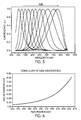
- FIG. 8 shows emission spectra of various quantum dot types when excited with ultraviolet radiation, according to one embodiment. These spectra are obtained by exciting the quantum dots with ultraviolet radiation while heating the quantum dot at about 60°C.
- the quantum dots are not imbedded in a matrix such as a polymer matrix. The quantum dots are spread on a substrate and excited with ultraviolet radiation. As shown in FIG.
- one type of quantum dots emits a peak of radiation (peak A) centered around about 600 nm
- another type of quantum dots emits a peak of radiation (peak B) centered around about 580 nm
- another type of quantum dots emits a peak of radiation (peak C) centered around about 630 nm
- another type of quantum dots emits a peak of radiation (peak D) centered around about 560 nm
- another type of quantum dots emits a peak of radiation (peak E) centered around about 620 nm.
- the above five types of quantum dots are spread as layers and stacked on a substrate. The stacked layers of quantum dots are then excited with ultraviolet radiation.
- the stacked layers of quantum dots emit a relatively broad spectrum of radiation (spectrum F) from about 540 nm to about 680 nm. This shows that a broad spectrum emitting radiation source can be created by using various types of quantum dots.
- FIG. 9 shows emission spectra of various quantum dot types when excited with ultraviolet radiation, according to another embodiment. These spectra are obtained by exciting the quantum dots with ultraviolet radiation without heating the quantum dots.
- the quantum dots are also not imbedded in a matrix such as a polymer matrix.
- the quantum dots are spread on a substrate and excited with ultraviolet radiation.
- one type of quantum dots emits peak (1) of radiation centered around about 620 nm
- another type of quantum dots emits peak (2) of radiation centered around about 600 nm
- another type of quantum dots emits peak (3) of radiation centered around about 560 nm.
- the above 3 types of quantum dots are spread as layers and stacked on a substrate. The stacked layers of quantum dots are then excited with ultraviolet radiation.
- the type of quantum dots emitting the peak of radiation (3) is deposited first on the substrate, followed by the type of quantum dots emitting the peak of radiation (2), then the type of quantum dots emitting the peak of radiation (1) to obtain a stack of quantum dots emitting a peak of radiation (4) centered around about 620 nm when excited with ultraviolet radiation.
- the type of quantum dots emitting the peak of radiation (1) is deposited first on the substrate, followed by the type of quantum dots emitting the peak of radiation (2), then the type of quantum dots emitting the peak of radiation (3) to obtain a stack of quantum dots emitting a peak of radiation (6) centered around about 620 nm when excited with ultraviolet radiation.
- the emission peak of the obtained stack of quantum dot layers is independent of the arrangement of the quantum dots layers in the stack.
- the quantum dots are not imbedded in a polymer matrix, however, as it can be appreciated the quantum dots can also be imbedded in a polymer matrix.
- the types of quantum dots emitting the various peak of radiation (1), (2) and (3) are mixed together to form a "cocktail" or mixture of quantum dots.
- the mixture of quantum dots is then excited with ultraviolet wavelength.
- the excited mixture of quantum dots emits a peak of radiation (5) centered around about 620 nm.
- the emission peak of radiation (5) obtained in the case of mixing the quantum dots and the emission peaks of radiation (4) and (6) obtained in the case of stacking the layers of the various types of quantum dots are substantially similar indicating that the resultant emission spectrum is independent from the relative position of the various types quantum dots.
- the selected quantum dots emit in the visible (VIS) wavelength range.
- different types of quantum dots can be selected by selecting a specific material (or chemical composition) of the quantum dots and/or selecting a size of the quantum dots so that the selected quantum dots emit in any range including VIS (between about 400 nm and about 800 nm), SWIR (between about 1 ⁇ m and about 3 ⁇ m), MWIR (between about 3 ⁇ m and about 8 ⁇ m) and LWIR (between about 8 ⁇ m and about 12 ⁇ m).
- VIS between about 400 nm and about 800 nm
- SWIR between about 1 ⁇ m and about 3 ⁇ m
- MWIR between about 3 ⁇ m and about 8 ⁇ m
- LWIR between about 8 ⁇ m and about 12 ⁇ m.
- a mixture of quantum dots can be selected so that the combined radiation emission spectrum of the quantum dots has a broad wavelength range to simulate the spectrum of sunlight.
- FIG. 10 shows a calibration system or calibrator using quantum dot based radiation source 10 shown in FIG. 1 for calibrating a detector, according to an embodiment.
- Calibration system 40 comprises quantum dot based radiation source 10 and integrating sphere 30.
- Inlet port 31 of integrating sphere 30 is connected to quantum dot based radiation source 10 via tube 19.
- Integrating sphere 30 operates generally in the same manner as described above with respect to integrating sphere 12 of quantum dot based radiation source 10.
- Radiation generated by the quantum dots of quantum dot based radiation source 10 is guided through tube 19 into integrating sphere 30 where the radiation is further reflected and diffused by a coating on an inner surface of wall 32 of integrating sphere 30.
- the radiation diffused in integrating sphere 30 is output through output port 34 of integrating sphere 30.
- Waveguide 36 may be provided to guide the radiation output from integrating sphere 30 towards detector 38, e.g., a focal plane array (FPA).
- Optics 37 e.g., a lens
- calibration system 40 can be calibrated so as to establish a relationship or link between the signal output by the detector and the photon flux emitted by an object under study.
- Calibration system 40 can be used, for example, in calibrating the signal output by space based radiometric instruments, such as instrument using an FPA detector for remote sensing applications.
- a detector e.g., FPA
- FPA a detector
- a detector can be, for example, configured to detect radiation with a sensitivity on the order of 100-200 photons in the SWIR wavelength, corresponding to a few picowatts to nanowatts in equivalent power.
- the radiation power P in Watts detected by a pixel in the FPA detector in space can be calculated by the following equation (1).
- P I ⁇ s ⁇ H f
- I is the intensity of the emitted or reflected light reaching the sensor from the object
- s is the area of a pixel on the FPA detector
- H is the altitude of the remote sensing instrument or the distance between the object and the FPA detector
- f is the focal length of the instrument's optics.
- the intensity I of light reaching the detector can be calculated by taking into account the location of the instrument at an altitude H. Indeed, the radiation intensity drops off at a rate corresponding to the inverse square law. Hence, if one assumes that the remote sensing instrument is at an altitude H of about 400 km above the earth's surface, the intensity I of the light reaching the remote sensing instrument (detector) will correspond to approximately 2.5 nW/m 2 . If the area of a pixel s is about 400 ⁇ m 2 (20 ⁇ m by 20 ⁇ m), and the focal length f is about 20 m, the obtained power P is about 2.10 -14 W.
- the total field of regard of the sensor is about 160,000 m 2 (0.16 km 2 ).
- the radiation power needed for calibrating the detector is the average power per pixel (determined using equation 1) multiplied by the field of regard.
- a power of a few nanowatts may be sufficient to calibrate the FPA detector with a million equally sized pixels.
- a power of a few microwatts net equivalent power can be output by the quantum dot based radiation source described in the above paragraphs, which is more than sufficient to serve as a calibration source.
Landscapes
- Physics & Mathematics (AREA)
- Spectroscopy & Molecular Physics (AREA)
- General Physics & Mathematics (AREA)
- Analytical Chemistry (AREA)
- Health & Medical Sciences (AREA)
- Life Sciences & Earth Sciences (AREA)
- Chemical & Material Sciences (AREA)
- Biochemistry (AREA)
- General Health & Medical Sciences (AREA)
- Immunology (AREA)
- Pathology (AREA)
- Theoretical Computer Science (AREA)
- Mathematical Physics (AREA)
- Engineering & Computer Science (AREA)
- Photometry And Measurement Of Optical Pulse Characteristics (AREA)
- Led Device Packages (AREA)
Applications Claiming Priority (1)
| Application Number | Priority Date | Filing Date | Title |
|---|---|---|---|
| US12/533,679 US8350223B2 (en) | 2009-07-31 | 2009-07-31 | Quantum dot based radiation source and radiometric calibrator using the same |
Publications (2)
| Publication Number | Publication Date |
|---|---|
| EP2280255A1 true EP2280255A1 (de) | 2011-02-02 |
| EP2280255B1 EP2280255B1 (de) | 2017-09-20 |
Family
ID=43087435
Family Applications (1)
| Application Number | Title | Priority Date | Filing Date |
|---|---|---|---|
| EP10164071.2A Active EP2280255B1 (de) | 2009-07-31 | 2010-05-27 | Quantumpunktbasierte Strahlungsquelle und radiometrischer Kalibrator damit |
Country Status (2)
| Country | Link |
|---|---|
| US (1) | US8350223B2 (de) |
| EP (1) | EP2280255B1 (de) |
Families Citing this family (10)
| Publication number | Priority date | Publication date | Assignee | Title |
|---|---|---|---|---|
| US8415759B2 (en) | 2010-11-23 | 2013-04-09 | Raytheon Company | Down-converting and detecting photons |
| US8507843B2 (en) * | 2011-05-20 | 2013-08-13 | Raytheon Company | Method and system for spectral calibration of a remote sensing sensor and a synthetic target having a tunable spectral composition |
| US9091748B2 (en) | 2012-04-18 | 2015-07-28 | Raytheon Company | Methods and apparatus for 3D UV imaging |
| US9488583B2 (en) * | 2012-12-31 | 2016-11-08 | Universiteit Gent | Molecular analysis device |
| US10711188B2 (en) | 2017-09-21 | 2020-07-14 | Raytheon Company | Process for producing quantum dots having broadened optical emission |
| KR102582064B1 (ko) * | 2018-07-11 | 2023-09-25 | 한국과학기술연구원 | 근적외선 흡수 염료 함유 나노입자, 이의 제조방법, 및 이의 용도 |
| JP7233239B2 (ja) * | 2019-02-18 | 2023-03-06 | 株式会社小糸製作所 | 塗料および被照射体の検知方法 |
| CN114402191A (zh) * | 2019-10-09 | 2022-04-26 | 松下知识产权经营株式会社 | 摄影装置 |
| US11297255B1 (en) | 2020-09-18 | 2022-04-05 | Raytheon Company | On-board light source calibration |
| CN114920460B (zh) * | 2022-05-02 | 2024-03-26 | 哈尔滨工程大学 | 一种双相量子点微晶玻璃及其制备方法和应用 |
Citations (9)
| Publication number | Priority date | Publication date | Assignee | Title |
|---|---|---|---|---|
| US6322901B1 (en) | 1997-11-13 | 2001-11-27 | Massachusetts Institute Of Technology | Highly luminescent color-selective nano-crystalline materials |
| US6344272B1 (en) | 1997-03-12 | 2002-02-05 | Wm. Marsh Rice University | Metal nanoshells |
| US20040145289A1 (en) * | 2003-01-27 | 2004-07-29 | 3M Innovative Properties Company | Phosphor based light sources having a non-planar short pass reflector and method of making |
| WO2004068597A2 (en) * | 2003-01-27 | 2004-08-12 | 3M Innovative Properties Company | Phosphor based light sources utilizing total internal reflection |
| DE102004047593A1 (de) * | 2004-09-30 | 2006-04-13 | Carl Zeiss Jena Gmbh | Referenzkörper für Fluoreszenzmessungen und Verfahren zur Herstellung desselben |
| EP1696224A2 (de) * | 2005-02-25 | 2006-08-30 | BAM Bundesanstalt für Materialforschung und -prüfung | Standard zur Referenzierung von Lumineszenzsignalen |
| US20060237636A1 (en) * | 2003-06-23 | 2006-10-26 | Advanced Optical Technologies, Llc | Integrating chamber LED lighting with pulse amplitude modulation to set color and/or intensity of output |
| EP1916719A2 (de) * | 2003-01-27 | 2008-04-30 | 3M Innovative Properties Company | Verfahren zur Herstellung von Lichtquellen auf Phosphorbasis mit Interferenzreflektor |
| WO2009002512A1 (en) * | 2007-06-25 | 2008-12-31 | Qd Vision, Inc. | Compositions, optical component, system including an optical component, devices, and other products |
Family Cites Families (13)
| Publication number | Priority date | Publication date | Assignee | Title |
|---|---|---|---|---|
| US6178865B1 (en) | 1983-03-23 | 2001-01-30 | The United States Of America As Represented By The Secretary Of The Army | Thermally massive radar decoy |
| US5505928A (en) | 1991-11-22 | 1996-04-09 | The Regents Of University Of California | Preparation of III-V semiconductor nanocrystals |
| US6501091B1 (en) | 1998-04-01 | 2002-12-31 | Massachusetts Institute Of Technology | Quantum dot white and colored light emitting diodes |
| US6338292B1 (en) | 1999-09-30 | 2002-01-15 | Robert Fisher Reynolds | Thermal and visual camouflage system |
| US20030044114A1 (en) * | 2001-09-06 | 2003-03-06 | Pelka David G. | Source wavelength shifting apparatus and method for delivery of one or more selected emission wavelengths |
| WO2004074739A1 (ja) * | 2003-02-21 | 2004-09-02 | Sanyo Electric Co., Ltd. | 発光素子及びディスプレイ |
| JP4789809B2 (ja) | 2004-01-15 | 2011-10-12 | サムスン エレクトロニクス カンパニー リミテッド | ナノ結晶をドーピングしたマトリックス |
| US7306963B2 (en) * | 2004-11-30 | 2007-12-11 | Spire Corporation | Precision synthesis of quantum dot nanostructures for fluorescent and optoelectronic devices |
| US7199344B2 (en) | 2005-03-11 | 2007-04-03 | The Boeing Company | Active camouflage using real-time spectral matching |
| US7482608B2 (en) * | 2005-04-20 | 2009-01-27 | Iso-Science Laboratories, Inc. | Nuclear powered quantum dot light source |
| US8050303B2 (en) | 2006-04-12 | 2011-11-01 | Raytheon Company | Laser based on quantum dot activated media with forster resonant energy transfer excitation |
| US7895880B2 (en) * | 2008-04-17 | 2011-03-01 | Honeywell International Inc. | Photoacoustic cell incorporating a quantum dot substrate |
| US8021008B2 (en) * | 2008-05-27 | 2011-09-20 | Abl Ip Holding Llc | Solid state lighting using quantum dots in a liquid |
-
2009
- 2009-07-31 US US12/533,679 patent/US8350223B2/en active Active
-
2010
- 2010-05-27 EP EP10164071.2A patent/EP2280255B1/de active Active
Patent Citations (9)
| Publication number | Priority date | Publication date | Assignee | Title |
|---|---|---|---|---|
| US6344272B1 (en) | 1997-03-12 | 2002-02-05 | Wm. Marsh Rice University | Metal nanoshells |
| US6322901B1 (en) | 1997-11-13 | 2001-11-27 | Massachusetts Institute Of Technology | Highly luminescent color-selective nano-crystalline materials |
| US20040145289A1 (en) * | 2003-01-27 | 2004-07-29 | 3M Innovative Properties Company | Phosphor based light sources having a non-planar short pass reflector and method of making |
| WO2004068597A2 (en) * | 2003-01-27 | 2004-08-12 | 3M Innovative Properties Company | Phosphor based light sources utilizing total internal reflection |
| EP1916719A2 (de) * | 2003-01-27 | 2008-04-30 | 3M Innovative Properties Company | Verfahren zur Herstellung von Lichtquellen auf Phosphorbasis mit Interferenzreflektor |
| US20060237636A1 (en) * | 2003-06-23 | 2006-10-26 | Advanced Optical Technologies, Llc | Integrating chamber LED lighting with pulse amplitude modulation to set color and/or intensity of output |
| DE102004047593A1 (de) * | 2004-09-30 | 2006-04-13 | Carl Zeiss Jena Gmbh | Referenzkörper für Fluoreszenzmessungen und Verfahren zur Herstellung desselben |
| EP1696224A2 (de) * | 2005-02-25 | 2006-08-30 | BAM Bundesanstalt für Materialforschung und -prüfung | Standard zur Referenzierung von Lumineszenzsignalen |
| WO2009002512A1 (en) * | 2007-06-25 | 2008-12-31 | Qd Vision, Inc. | Compositions, optical component, system including an optical component, devices, and other products |
Also Published As
| Publication number | Publication date |
|---|---|
| US20110024612A1 (en) | 2011-02-03 |
| EP2280255B1 (de) | 2017-09-20 |
| US8350223B2 (en) | 2013-01-08 |
Similar Documents
| Publication | Publication Date | Title |
|---|---|---|
| EP2280255B1 (de) | Quantumpunktbasierte Strahlungsquelle und radiometrischer Kalibrator damit | |
| KR102293477B1 (ko) | 광학 특성 측정 시스템의 교정 방법 | |
| Yoshizawa | Handbook of optical metrology: Principles and Applications | |
| US10054485B2 (en) | UV LED-phosphor based hyperspectral calibrator | |
| US10182702B2 (en) | Light-emitting apparatus including photoluminescent layer | |
| Gorrotxategi et al. | Optical efficiency characterization of LED phosphors using a double integrating sphere system | |
| JP5608919B2 (ja) | 光学測定装置 | |
| USRE49093E1 (en) | Light-emitting apparatus including photoluminescent layer | |
| RU2648980C2 (ru) | Испускающий свет узел, лампа и осветительный прибор | |
| US9212968B1 (en) | Onboard calibration source for spectral calibraton of a radiometer | |
| CN104302986A (zh) | 光收集器设备 | |
| US20140247442A1 (en) | Spectroradiometer device and applications of same | |
| JP5683834B2 (ja) | 測光装置 | |
| CN109639362A (zh) | 一种基于散射效应的多输入多输出光通信系统及通信方法 | |
| Aphalo | Neutral density filters: theory vs. reality | |
| Wang | Radiometry and Photometry | |
| Marshall et al. | DECal: A Spectrophotometric Calibration System For DECam | |
| Krisciunas | The Usefulness of Type Ia Supernovae for Cosmology-A Personal Review | |
| Dushkina | Light sources | |
| JP6681632B2 (ja) | 光学特性測定システムの校正方法 | |
| Eppeldauer | Uniform calibration of night vision goggles and test sets | |
| Jaanson et al. | A reference material with close to Lambertian reflectance and fluorescence emission profiles | |
| Al-Bahadly et al. | LED-Based Colour Sensing System | |
| JP4336775B2 (ja) | 光学測定方法、発光素子の測定方法および発光素子の測定装置 | |
| Russell et al. | The Challenges of 1% Uncertainty in Optical Ground Support Equipment Calibrations |
Legal Events
| Date | Code | Title | Description |
|---|---|---|---|
| PUAI | Public reference made under article 153(3) epc to a published international application that has entered the european phase |
Free format text: ORIGINAL CODE: 0009012 |
|
| AK | Designated contracting states |
Kind code of ref document: A1 Designated state(s): AL AT BE BG CH CY CZ DE DK EE ES FI FR GB GR HR HU IE IS IT LI LT LU LV MC MK MT NL NO PL PT RO SE SI SK SM TR |
|
| AX | Request for extension of the european patent |
Extension state: BA ME RS |
|
| 17P | Request for examination filed |
Effective date: 20110801 |
|
| 17Q | First examination report despatched |
Effective date: 20141029 |
|
| GRAP | Despatch of communication of intention to grant a patent |
Free format text: ORIGINAL CODE: EPIDOSNIGR1 |
|
| INTG | Intention to grant announced |
Effective date: 20170504 |
|
| GRAS | Grant fee paid |
Free format text: ORIGINAL CODE: EPIDOSNIGR3 |
|
| GRAA | (expected) grant |
Free format text: ORIGINAL CODE: 0009210 |
|
| AK | Designated contracting states |
Kind code of ref document: B1 Designated state(s): AL AT BE BG CH CY CZ DE DK EE ES FI FR GB GR HR HU IE IS IT LI LT LU LV MC MK MT NL NO PL PT RO SE SI SK SM TR |
|
| REG | Reference to a national code |
Ref country code: GB Ref legal event code: FG4D |
|
| REG | Reference to a national code |
Ref country code: CH Ref legal event code: EP |
|
| REG | Reference to a national code |
Ref country code: AT Ref legal event code: REF Ref document number: 930538 Country of ref document: AT Kind code of ref document: T Effective date: 20171015 |
|
| REG | Reference to a national code |
Ref country code: IE Ref legal event code: FG4D |
|
| REG | Reference to a national code |
Ref country code: DE Ref legal event code: R096 Ref document number: 602010045324 Country of ref document: DE |
|
| REG | Reference to a national code |
Ref country code: NL Ref legal event code: MP Effective date: 20170920 |
|
| PG25 | Lapsed in a contracting state [announced via postgrant information from national office to epo] |
Ref country code: FI Free format text: LAPSE BECAUSE OF FAILURE TO SUBMIT A TRANSLATION OF THE DESCRIPTION OR TO PAY THE FEE WITHIN THE PRESCRIBED TIME-LIMIT Effective date: 20170920 Ref country code: HR Free format text: LAPSE BECAUSE OF FAILURE TO SUBMIT A TRANSLATION OF THE DESCRIPTION OR TO PAY THE FEE WITHIN THE PRESCRIBED TIME-LIMIT Effective date: 20170920 Ref country code: LT Free format text: LAPSE BECAUSE OF FAILURE TO SUBMIT A TRANSLATION OF THE DESCRIPTION OR TO PAY THE FEE WITHIN THE PRESCRIBED TIME-LIMIT Effective date: 20170920 Ref country code: SE Free format text: LAPSE BECAUSE OF FAILURE TO SUBMIT A TRANSLATION OF THE DESCRIPTION OR TO PAY THE FEE WITHIN THE PRESCRIBED TIME-LIMIT Effective date: 20170920 Ref country code: NO Free format text: LAPSE BECAUSE OF FAILURE TO SUBMIT A TRANSLATION OF THE DESCRIPTION OR TO PAY THE FEE WITHIN THE PRESCRIBED TIME-LIMIT Effective date: 20171220 |
|
| REG | Reference to a national code |
Ref country code: LT Ref legal event code: MG4D |
|
| REG | Reference to a national code |
Ref country code: AT Ref legal event code: MK05 Ref document number: 930538 Country of ref document: AT Kind code of ref document: T Effective date: 20170920 |
|
| PG25 | Lapsed in a contracting state [announced via postgrant information from national office to epo] |
Ref country code: BG Free format text: LAPSE BECAUSE OF FAILURE TO SUBMIT A TRANSLATION OF THE DESCRIPTION OR TO PAY THE FEE WITHIN THE PRESCRIBED TIME-LIMIT Effective date: 20171220 Ref country code: GR Free format text: LAPSE BECAUSE OF FAILURE TO SUBMIT A TRANSLATION OF THE DESCRIPTION OR TO PAY THE FEE WITHIN THE PRESCRIBED TIME-LIMIT Effective date: 20171221 Ref country code: LV Free format text: LAPSE BECAUSE OF FAILURE TO SUBMIT A TRANSLATION OF THE DESCRIPTION OR TO PAY THE FEE WITHIN THE PRESCRIBED TIME-LIMIT Effective date: 20170920 |
|
| PG25 | Lapsed in a contracting state [announced via postgrant information from national office to epo] |
Ref country code: NL Free format text: LAPSE BECAUSE OF FAILURE TO SUBMIT A TRANSLATION OF THE DESCRIPTION OR TO PAY THE FEE WITHIN THE PRESCRIBED TIME-LIMIT Effective date: 20170920 |
|
| REG | Reference to a national code |
Ref country code: FR Ref legal event code: PLFP Year of fee payment: 9 |
|
| PG25 | Lapsed in a contracting state [announced via postgrant information from national office to epo] |
Ref country code: ES Free format text: LAPSE BECAUSE OF FAILURE TO SUBMIT A TRANSLATION OF THE DESCRIPTION OR TO PAY THE FEE WITHIN THE PRESCRIBED TIME-LIMIT Effective date: 20170920 Ref country code: CZ Free format text: LAPSE BECAUSE OF FAILURE TO SUBMIT A TRANSLATION OF THE DESCRIPTION OR TO PAY THE FEE WITHIN THE PRESCRIBED TIME-LIMIT Effective date: 20170920 Ref country code: PL Free format text: LAPSE BECAUSE OF FAILURE TO SUBMIT A TRANSLATION OF THE DESCRIPTION OR TO PAY THE FEE WITHIN THE PRESCRIBED TIME-LIMIT Effective date: 20170920 Ref country code: RO Free format text: LAPSE BECAUSE OF FAILURE TO SUBMIT A TRANSLATION OF THE DESCRIPTION OR TO PAY THE FEE WITHIN THE PRESCRIBED TIME-LIMIT Effective date: 20170920 |
|
| PG25 | Lapsed in a contracting state [announced via postgrant information from national office to epo] |
Ref country code: EE Free format text: LAPSE BECAUSE OF FAILURE TO SUBMIT A TRANSLATION OF THE DESCRIPTION OR TO PAY THE FEE WITHIN THE PRESCRIBED TIME-LIMIT Effective date: 20170920 Ref country code: SK Free format text: LAPSE BECAUSE OF FAILURE TO SUBMIT A TRANSLATION OF THE DESCRIPTION OR TO PAY THE FEE WITHIN THE PRESCRIBED TIME-LIMIT Effective date: 20170920 Ref country code: IT Free format text: LAPSE BECAUSE OF FAILURE TO SUBMIT A TRANSLATION OF THE DESCRIPTION OR TO PAY THE FEE WITHIN THE PRESCRIBED TIME-LIMIT Effective date: 20170920 Ref country code: IS Free format text: LAPSE BECAUSE OF FAILURE TO SUBMIT A TRANSLATION OF THE DESCRIPTION OR TO PAY THE FEE WITHIN THE PRESCRIBED TIME-LIMIT Effective date: 20180120 Ref country code: AT Free format text: LAPSE BECAUSE OF FAILURE TO SUBMIT A TRANSLATION OF THE DESCRIPTION OR TO PAY THE FEE WITHIN THE PRESCRIBED TIME-LIMIT Effective date: 20170920 Ref country code: SM Free format text: LAPSE BECAUSE OF FAILURE TO SUBMIT A TRANSLATION OF THE DESCRIPTION OR TO PAY THE FEE WITHIN THE PRESCRIBED TIME-LIMIT Effective date: 20170920 |
|
| REG | Reference to a national code |
Ref country code: DE Ref legal event code: R097 Ref document number: 602010045324 Country of ref document: DE |
|
| PLBE | No opposition filed within time limit |
Free format text: ORIGINAL CODE: 0009261 |
|
| STAA | Information on the status of an ep patent application or granted ep patent |
Free format text: STATUS: NO OPPOSITION FILED WITHIN TIME LIMIT |
|
| PG25 | Lapsed in a contracting state [announced via postgrant information from national office to epo] |
Ref country code: DK Free format text: LAPSE BECAUSE OF FAILURE TO SUBMIT A TRANSLATION OF THE DESCRIPTION OR TO PAY THE FEE WITHIN THE PRESCRIBED TIME-LIMIT Effective date: 20170920 |
|
| 26N | No opposition filed |
Effective date: 20180621 |
|
| PG25 | Lapsed in a contracting state [announced via postgrant information from national office to epo] |
Ref country code: SI Free format text: LAPSE BECAUSE OF FAILURE TO SUBMIT A TRANSLATION OF THE DESCRIPTION OR TO PAY THE FEE WITHIN THE PRESCRIBED TIME-LIMIT Effective date: 20170920 |
|
| REG | Reference to a national code |
Ref country code: CH Ref legal event code: PL |
|
| REG | Reference to a national code |
Ref country code: BE Ref legal event code: MM Effective date: 20180531 |
|
| PG25 | Lapsed in a contracting state [announced via postgrant information from national office to epo] |
Ref country code: MC Free format text: LAPSE BECAUSE OF FAILURE TO SUBMIT A TRANSLATION OF THE DESCRIPTION OR TO PAY THE FEE WITHIN THE PRESCRIBED TIME-LIMIT Effective date: 20170920 |
|
| REG | Reference to a national code |
Ref country code: IE Ref legal event code: MM4A |
|
| PG25 | Lapsed in a contracting state [announced via postgrant information from national office to epo] |
Ref country code: LI Free format text: LAPSE BECAUSE OF NON-PAYMENT OF DUE FEES Effective date: 20180531 Ref country code: CH Free format text: LAPSE BECAUSE OF NON-PAYMENT OF DUE FEES Effective date: 20180531 |
|
| PG25 | Lapsed in a contracting state [announced via postgrant information from national office to epo] |
Ref country code: LU Free format text: LAPSE BECAUSE OF NON-PAYMENT OF DUE FEES Effective date: 20180527 |
|
| PG25 | Lapsed in a contracting state [announced via postgrant information from national office to epo] |
Ref country code: IE Free format text: LAPSE BECAUSE OF NON-PAYMENT OF DUE FEES Effective date: 20180527 |
|
| PG25 | Lapsed in a contracting state [announced via postgrant information from national office to epo] |
Ref country code: BE Free format text: LAPSE BECAUSE OF NON-PAYMENT OF DUE FEES Effective date: 20180531 |
|
| PG25 | Lapsed in a contracting state [announced via postgrant information from national office to epo] |
Ref country code: MT Free format text: LAPSE BECAUSE OF NON-PAYMENT OF DUE FEES Effective date: 20180527 |
|
| PG25 | Lapsed in a contracting state [announced via postgrant information from national office to epo] |
Ref country code: TR Free format text: LAPSE BECAUSE OF FAILURE TO SUBMIT A TRANSLATION OF THE DESCRIPTION OR TO PAY THE FEE WITHIN THE PRESCRIBED TIME-LIMIT Effective date: 20170920 |
|
| PG25 | Lapsed in a contracting state [announced via postgrant information from national office to epo] |
Ref country code: HU Free format text: LAPSE BECAUSE OF FAILURE TO SUBMIT A TRANSLATION OF THE DESCRIPTION OR TO PAY THE FEE WITHIN THE PRESCRIBED TIME-LIMIT; INVALID AB INITIO Effective date: 20100527 Ref country code: PT Free format text: LAPSE BECAUSE OF FAILURE TO SUBMIT A TRANSLATION OF THE DESCRIPTION OR TO PAY THE FEE WITHIN THE PRESCRIBED TIME-LIMIT Effective date: 20170920 |
|
| PG25 | Lapsed in a contracting state [announced via postgrant information from national office to epo] |
Ref country code: CY Free format text: LAPSE BECAUSE OF FAILURE TO SUBMIT A TRANSLATION OF THE DESCRIPTION OR TO PAY THE FEE WITHIN THE PRESCRIBED TIME-LIMIT Effective date: 20170920 Ref country code: MK Free format text: LAPSE BECAUSE OF NON-PAYMENT OF DUE FEES Effective date: 20170920 |
|
| PG25 | Lapsed in a contracting state [announced via postgrant information from national office to epo] |
Ref country code: AL Free format text: LAPSE BECAUSE OF FAILURE TO SUBMIT A TRANSLATION OF THE DESCRIPTION OR TO PAY THE FEE WITHIN THE PRESCRIBED TIME-LIMIT Effective date: 20170920 |
|
| P01 | Opt-out of the competence of the unified patent court (upc) registered |
Effective date: 20230530 |
|
| PGFP | Annual fee paid to national office [announced via postgrant information from national office to epo] |
Ref country code: FR Payment date: 20230420 Year of fee payment: 14 Ref country code: DE Payment date: 20230419 Year of fee payment: 14 |
|
| PGFP | Annual fee paid to national office [announced via postgrant information from national office to epo] |
Ref country code: GB Payment date: 20230420 Year of fee payment: 14 |