EP2275861B1 - Active matrix substrate, display device, method for inspecting active matrix substrate, and method for inspecting display device - Google Patents
Active matrix substrate, display device, method for inspecting active matrix substrate, and method for inspecting display device Download PDFInfo
- Publication number
- EP2275861B1 EP2275861B1 EP09746497.8A EP09746497A EP2275861B1 EP 2275861 B1 EP2275861 B1 EP 2275861B1 EP 09746497 A EP09746497 A EP 09746497A EP 2275861 B1 EP2275861 B1 EP 2275861B1
- Authority
- EP
- European Patent Office
- Prior art keywords
- wirings
- inspection
- switching elements
- wiring
- inspection wiring
- Prior art date
- Legal status (The legal status is an assumption and is not a legal conclusion. Google has not performed a legal analysis and makes no representation as to the accuracy of the status listed.)
- Not-in-force
Links
Images


Classifications
-
- G—PHYSICS
- G02—OPTICS
- G02F—OPTICAL DEVICES OR ARRANGEMENTS FOR THE CONTROL OF LIGHT BY MODIFICATION OF THE OPTICAL PROPERTIES OF THE MEDIA OF THE ELEMENTS INVOLVED THEREIN; NON-LINEAR OPTICS; FREQUENCY-CHANGING OF LIGHT; OPTICAL LOGIC ELEMENTS; OPTICAL ANALOGUE/DIGITAL CONVERTERS
- G02F1/00—Devices or arrangements for the control of the intensity, colour, phase, polarisation or direction of light arriving from an independent light source, e.g. switching, gating or modulating; Non-linear optics
- G02F1/01—Devices or arrangements for the control of the intensity, colour, phase, polarisation or direction of light arriving from an independent light source, e.g. switching, gating or modulating; Non-linear optics for the control of the intensity, phase, polarisation or colour
- G02F1/13—Devices or arrangements for the control of the intensity, colour, phase, polarisation or direction of light arriving from an independent light source, e.g. switching, gating or modulating; Non-linear optics for the control of the intensity, phase, polarisation or colour based on liquid crystals, e.g. single liquid crystal display cells
- G02F1/133—Constructional arrangements; Operation of liquid crystal cells; Circuit arrangements
- G02F1/136—Liquid crystal cells structurally associated with a semi-conducting layer or substrate, e.g. cells forming part of an integrated circuit
- G02F1/1362—Active matrix addressed cells
- G02F1/136286—Wiring, e.g. gate line, drain line
-
- G—PHYSICS
- G02—OPTICS
- G02F—OPTICAL DEVICES OR ARRANGEMENTS FOR THE CONTROL OF LIGHT BY MODIFICATION OF THE OPTICAL PROPERTIES OF THE MEDIA OF THE ELEMENTS INVOLVED THEREIN; NON-LINEAR OPTICS; FREQUENCY-CHANGING OF LIGHT; OPTICAL LOGIC ELEMENTS; OPTICAL ANALOGUE/DIGITAL CONVERTERS
- G02F1/00—Devices or arrangements for the control of the intensity, colour, phase, polarisation or direction of light arriving from an independent light source, e.g. switching, gating or modulating; Non-linear optics
- G02F1/01—Devices or arrangements for the control of the intensity, colour, phase, polarisation or direction of light arriving from an independent light source, e.g. switching, gating or modulating; Non-linear optics for the control of the intensity, phase, polarisation or colour
- G02F1/13—Devices or arrangements for the control of the intensity, colour, phase, polarisation or direction of light arriving from an independent light source, e.g. switching, gating or modulating; Non-linear optics for the control of the intensity, phase, polarisation or colour based on liquid crystals, e.g. single liquid crystal display cells
- G02F1/133—Constructional arrangements; Operation of liquid crystal cells; Circuit arrangements
- G02F1/1333—Constructional arrangements; Manufacturing methods
- G02F1/1345—Conductors connecting electrodes to cell terminals
- G02F1/13456—Cell terminals located on one side of the display only
-
- G—PHYSICS
- G02—OPTICS
- G02F—OPTICAL DEVICES OR ARRANGEMENTS FOR THE CONTROL OF LIGHT BY MODIFICATION OF THE OPTICAL PROPERTIES OF THE MEDIA OF THE ELEMENTS INVOLVED THEREIN; NON-LINEAR OPTICS; FREQUENCY-CHANGING OF LIGHT; OPTICAL LOGIC ELEMENTS; OPTICAL ANALOGUE/DIGITAL CONVERTERS
- G02F1/00—Devices or arrangements for the control of the intensity, colour, phase, polarisation or direction of light arriving from an independent light source, e.g. switching, gating or modulating; Non-linear optics
- G02F1/01—Devices or arrangements for the control of the intensity, colour, phase, polarisation or direction of light arriving from an independent light source, e.g. switching, gating or modulating; Non-linear optics for the control of the intensity, phase, polarisation or colour
- G02F1/13—Devices or arrangements for the control of the intensity, colour, phase, polarisation or direction of light arriving from an independent light source, e.g. switching, gating or modulating; Non-linear optics for the control of the intensity, phase, polarisation or colour based on liquid crystals, e.g. single liquid crystal display cells
- G02F1/133—Constructional arrangements; Operation of liquid crystal cells; Circuit arrangements
- G02F1/136—Liquid crystal cells structurally associated with a semi-conducting layer or substrate, e.g. cells forming part of an integrated circuit
- G02F1/1362—Active matrix addressed cells
- G02F1/136254—Checking; Testing
-
- G—PHYSICS
- G02—OPTICS
- G02F—OPTICAL DEVICES OR ARRANGEMENTS FOR THE CONTROL OF LIGHT BY MODIFICATION OF THE OPTICAL PROPERTIES OF THE MEDIA OF THE ELEMENTS INVOLVED THEREIN; NON-LINEAR OPTICS; FREQUENCY-CHANGING OF LIGHT; OPTICAL LOGIC ELEMENTS; OPTICAL ANALOGUE/DIGITAL CONVERTERS
- G02F1/00—Devices or arrangements for the control of the intensity, colour, phase, polarisation or direction of light arriving from an independent light source, e.g. switching, gating or modulating; Non-linear optics
- G02F1/01—Devices or arrangements for the control of the intensity, colour, phase, polarisation or direction of light arriving from an independent light source, e.g. switching, gating or modulating; Non-linear optics for the control of the intensity, phase, polarisation or colour
- G02F1/13—Devices or arrangements for the control of the intensity, colour, phase, polarisation or direction of light arriving from an independent light source, e.g. switching, gating or modulating; Non-linear optics for the control of the intensity, phase, polarisation or colour based on liquid crystals, e.g. single liquid crystal display cells
- G02F1/133—Constructional arrangements; Operation of liquid crystal cells; Circuit arrangements
- G02F1/136—Liquid crystal cells structurally associated with a semi-conducting layer or substrate, e.g. cells forming part of an integrated circuit
- G02F1/1362—Active matrix addressed cells
- G02F1/136286—Wiring, e.g. gate line, drain line
- G02F1/13629—Multilayer wirings
-
- H—ELECTRICITY
- H10—SEMICONDUCTOR DEVICES; ELECTRIC SOLID-STATE DEVICES NOT OTHERWISE PROVIDED FOR
- H10K—ORGANIC ELECTRIC SOLID-STATE DEVICES
- H10K59/00—Integrated devices, or assemblies of multiple devices, comprising at least one organic light-emitting element covered by group H10K50/00
- H10K59/10—OLED displays
- H10K59/12—Active-matrix OLED [AMOLED] displays
- H10K59/131—Interconnections, e.g. wiring lines or terminals
Definitions
- a plurality of first extension wirings 53 respectively extending toward the first side S 1 from the plurality of scan terminals 51 connected to the right-side scan connecting wirings 61 1 to 61 7 are connected to the plurality of the scan terminals 51.
- a first inspection wiring (seventh inspection wiring) 63 for scan wirings is connected to the plurality of first extension wirings 53. That is, the first inspection wiring 63 for scan wirings is connected to each of the plurality of first extension wirings 53.
- a first inspection pad 64 for scan wirings is further connected to the first inspection wiring 63 for scan wirings.
- the first inspection pad 64 for scan wirings is a pad through which scan inspection signals can be input. Note that scan inspection signals are inspection signals that functions as scan signals.
- the left-side scan connecting wirings 65 1 to 65 6 include first left-side scan connecting wirings (third connecting wirings, sixth connecting wirings) 65 1 , 65 3 and 65 5 , and second left-side scan connecting wirings (fourth connecting wirings, eighth connecting wirings) 65 2 , 65 4 and 65 6 .
- the first left-side scan connecting wirings 65 1 , 65 3 and 65 5 are wirings that are formed on the first layer.
- the second left-side scan connecting wirings 65 2 , 65 4 and 65 6 are wirings of which at least a portion is formed on the second layer
- the second inspection wiring 77 for left-side scan connecting wirings is an inspection wiring capable of inputting scan inspection signals to the non-adjacent first left-side scan switching element 74 3 that is not connected to the first inspection wiring 75 for left-side scan connecting wirings among the first left-side scan switching elements 74 1 , 74 3 and 74 5 , and to the non-adjacent second left-side scan switching element 74 2 and 74 6 that are not connected to the first inspection wiring 75 for left-side scan connecting wirings among the second left-side scan switching elements 74 2 , 74 4 and 74 6 .
- the second inspection wiring 77 for left-side scan connecting wirings is formed in the peripheral wiring region 6 so as to intersect each of the left-side scan connecting wirings 65 1 to 65 6 .
- data connecting wirings (second connecting wirings) 81 1 , 81 2 , 81 3 , ...81 i respectively connecting the data terminals 52 and the input ends 45 1 , 45 2 , 45 3 , ...45 i for data signals provided at one end of the data wirings 42 1 , 42 2 , 42 3 , ...42 i are formed in the peripheral wiring region 6. That is, the data connecting wirings 81 are extracted from the input ends 44 for data signals toward the first side S 1 , and connected to the data terminals 52. Note that in FIG. 1 , the data connecting wirings 81 1 , 81 2 , 81 3 , ...81 i are represented simply as 81.
- the first inspection wiring 70 for right-side scan connecting wirings and the second inspection wiring 72 for right-side scan connecting wirings are adjacent to each other, and all of the right-side scan switching elements 69 1 to 69 7 are formed between the first inspection wiring 70 for right-side scan connecting wirings and the second inspection wiring 72 for right-side scan connecting wirings.
- the first inspection wiring 75 for left-side scan connecting wirings and the second inspection wiring 77 for left-side scan connecting wirings are adjacent to each other, and all of the left-side scan switching elements 74 1 to 74 6 are formed between the first inspection wiring 75 for left-side scan connecting wirings and the second inspection wiring 77 for left-side scan connecting wirings.
- the two base substrates are then adhered together after the sealant has been applied
- the two base substrates adhered together are then sectioned as mother substrates from which a prescribed number of liquid crystal panels 1 having an active matrix substrate 2 and an opposing substrate 3 are formed.
- Aliquid crystal material is injected into each of the liquid crystal panel 1 sectioned as mother substrates using a vacuum injection method, for example, through an inlet formed between the active matrix substrate 2 and the opposing substrate 3.
- the liquid crystal material may be injected using a drop injection method rather than a vacuum injection method. In this case, neither the inlet nor a process of sealing the inlet portion is required.
- the liquid crystal panel 1 shown in FIG. 1 is a single liquid crystal panel that has been sectioned as a mother substrate and injected with a liquid crystal material. Accordingly, although illustration thereof has been omitted, other liquid crystal panels exist above, below and to the left and right of the liquid crystal panel 1 shown in FIG. 1 .
- scan inspection signals are collectively input to the right-side scan connecting wirings 61 1 to 61 7 from the first inspection pad 64 for scan wirings. That is, the same scan inspection signal is input to each of the adjacent first right-side scan connecting wirings 61 1 , 61 3 , 61 5 and 61 7 formed on the first layer. In other words, the adjacent first right-side scan connecting wirings 61 1 , 61 3 , 61 5 and 61 7 have the same potential. Also, the same scan inspection signal is input to each of the adjacent second right-side scan connecting wirings 61 2 , 61 4 and 61 6 formed on the second layer.
- the present invention can, naturally, also be applied to an IPS (In-Plane Switching) mode liquid crystal panel in which common electrodes are formed on an active matrix substrate.
- IPS In-Plane Switching
- a transfer pad need not be formed on the active matrix substrate of an IPS mode liquid crystal paneL
- MVA Multi-Domain Vertical Aligned
- OCB Optically Compensated Bend
Description
- The present invention relates to an active matrix substrate having two or more layers, with a plurality of first connecting wirings respectively connecting a plurality of first wirings formed parallel to each other in a display region and a plurality of first terminals arranged in a terminal arrangement region being formed on the respective layers, a display device, a method for inspecting the active matrix substrate, and a method for inspecting the display device.
- In recent years, liquid crystal panels have been widely used in a variety of electronic devices such as mobile phones, PDAs, car navigation systems and personal computers. Liquid crystal panels are characterized by being thin, lightweight and power efficient. As for methods of mounting drivers on such liquid crystal panels, a so-called COG (Chip On Glass) method that involves directly mounting a driver on one (active matrix substrate) of a pair of substrates opposing each other across a liquid crystal material is known (e.g., see
JP 2003-172944A JP 2005-301308A JP 2003-241217A JP 2004-325956A JP 2005-241988A WO 2008/015808A ). Using this COG method enables liquid crystal panels to be made thinner, smaller and lighter, and with higher definition between wirings and terminal. - Also, the vertical and horizontal pixel count of the display screens of liquid crystal panels used in compact electronic devices such as mobile phones and PDAs has transitioned in recent years from 160 × 120 QQVGA (Quarter Quarter Video Graphics Array) and 176 × 144 QCIF (Quarter Common Intermediate Format) to 320 × 240 QVGA (Quarter Video Graphics Array) and even 640 × 480 VGA (Video Graphics Array). This has lead to an increase in the number of wirings and terminals that ought to be formed on an active matrix substrate constituting a liquid crystal panel. However, in order to address the demand for more compact and higher definition liquid crystal panels, the size of the active matrix substrate cannot be increased.
- In view of this, an active matrix substrate on which a plurality of connecting wirings respectively connecting a plurality of scan wirings formed in a display region and a plurality of scan terminals arranged in a terminal arrangement region are formed on two or more layers (multi-layers) is known (e.g., see
JP 2004-53702A JP 2005-91962A -
EP-A-2 264 689 is cited as prior art within the meaning of Art. 54(3) EPC and shows a very similar wiring scheme as the present application, however, there is no disclosure of wirings being arranged in different layers. - An active matrix substrate as defined in the preamble of
claim 1 is known fromWO2008/015808 . - Incidentally, because an insulating material is interposed between the connecting wirings formed on the first layer and the connecting wirings formed on the second layer, short circuits (leakage) are unlikely to occur between the connecting wirings formed on the first layer and the connecting wirings formed on the second layer. However, short circuits can occur between adjacent connecting wirings formed on the same layer, caused by dust in the photolithography process, etching residue or the like during manufacture of the active matrix substrate. In particular, in recent years, more compact and higher definition liquid crystal panels have been desired, as discussed above, increasing the likelihood of short circuits between adjacent connecting wirings formed on the same layer, since the spacing between wirings has been increasingly reduced in recent years. The importance of inspecting for short circuit between connecting wirings in the inspection process during manufacture or the like of active matrix substrates has thus increased. That is, in the mounting process, mounting a driver on a defective active matrix substrate in which a wiring short circuit has occurred results in a loss of material costs and operating costs.
- However, despite the increasing importance of inspecting for short circuits between connecting wirings, a mechanism for detecting short circuits between adjacent connecting wirings formed on the same layer in relation to each of a plurality of layers in an active matrix substrate having two or more layers has not been established. In the abovementioned patent documents (e.g., see
JP 2003-172944A JP 2005-301308A JP 2003-241217A JP 2004-325956A JP 2005-241988A WO 2008/015808A ,JP 2004-53702A JP 2005-91962A - The present invention has been made in consideration of the above problems, and has as its object to provide an active matrix substrate, a display device, a method for inspecting the active matrix substrate and a method for inspecting the display device that enable short circuits between adjacent connecting wirings formed on the same layer to be reliably detected with a simple configuration in relation to each of a plurality of layers.
- In order to attain the above object, an active matrix substrate according to the present invention is defined in
claim 1. - According to the active matrix substrate of the present invention, inspection signals can be input to the third connecting wirings via the first switching elements by inputting mutually independent inspection signals to the first inspection wiring and the second inspection wiring while maintaining the first switching elements in an ON state, in an inspection process during manufacture or the like of the active matrix substrate. That is, mutually independent inspection signals can be input to adjacent third connecting wirings. Short circuits between adjacent third connecting wirings can thereby be detected. Note that the third connecting wirings are formed on the same layer as the layer on which the first wirings are formed.
- Also, inspection signals can be input to the fourth connecting wirings via the second switching elements by inputting mutually independent inspection signals to the first inspection wiring and the second inspection wiring while maintaining the second switching elements in an ON state. That is, mutually independent inspection signals can be input to adjacent fourth connecting wirings. Short circuits between adjacent fourth connecting wirings can thereby be detected. Note that at least a portion of the fourth connecting wirings is formed on a different layer from the layer on which the first wirings are formed with an insulating material sandwiched therebetween.
- Also, inspection wirings for inspecting for short circuits between adjacent third connecting wirings and inspection wirings for inspecting for short circuits between adjacent fourth connecting wirings are jointly the first inspection wiring and the second inspection wiring. The number of inspection wirings to be formed on an active matrix substrate can thus be reduced, in comparison with a mode in which inspection wirings for inspecting for short circuits between adjacent third connecting wirings and inspection wirings for inspecting for short circuits between adjacent fourth connecting wirings are respectively configured as discrete inspection wirings. Further, since the number of inspection wirings can be reduced, the system for inputting inspection signals can be reduced, and inspection can be implemented with a simple inspection device.
- As a result, an active matrix substrate that enables short circuits between adjacent connecting wirings formed on the same layer to be reliably detected with a simple configuration in relation to each of a plurality of layers can be realized.
- In order to attain the above object, a display device in the present invention is provided with an active matrix substrate according to the present invention. Note that the display device preferably is a liquid crystal display device.
- In order to attain the above object, a method for inspecting an active matrix substrate or a display device in the present invention includes a process of inspecting the third connecting wirings by inputting mutually independent inspection signals to the first inspection wiring and the second inspection wiring while maintaining the first switching elements in an ON state, and a process of inspecting the fourth connecting wirings by inputting mutually independent inspection signals to the first inspection wiring and the second inspection wiring while maintaining the second switching elements in an ON state.
- According to the method for inspecting an active matrix substrate or a display device of the present invention, short circuits of the third connecting wirings formed on the same layer as the layer on which the first wirings are formed can be detected, by inputting mutually independent inspection signals to the first inspection wiring and the second inspection wiring, while maintaining the first switching elements in an ON state. Also, short circuits of the fourth connecting wirings, at least a portion of which is formed on a different layer to the layer on which the first wirings are formed, can be detected, by inputting mutually independent inspection signals to the first inspection wiring and the second inspection wiring, while maintaining the second switching elements in an ON state. Note that the process of inspecting the third connecting wirings may be upstream or downstream of the process of inspecting the fourth connecting wirings.
- As described above, an active matrix substrate, a display device and a method for inspecting the active matrix substrate of the present invention accomplish the effect of enabling short circuits between adjacent connecting wirings formed on the same layer to be reliably detected with a simple configuration in relation to each of a plurality of layers.
-
-
FIG. 1 is a plan view showing a schematic configuration of a liquid crystal panel according to an embodiment. -
FIG. 2 is a cross-sectional view sectioned along a section line a-a'shown inFIG. 1 . -
FIG. 3 is a cross-sectional view showing a schematic configuration of another liquid crystal panel according to the embodiment at the same location as that shown inFIG. 2 . -
FIG. 4 is a plan view showing a schematic configuration of another liquid crystal panel according to an illustrative example for explaining the embodiment. -
FIG. 5 is an illustrative diagram showing an enlarged view of an E portion shown inFIG. 1 . -
FIG. 6 is an illustrative diagram showing a portion of another active matrix substrate according to the embodiment at the same location as that shown inFIG. 5 . -
FIG. 7 is an illustrative diagram showing a portion of another active matrix substrate according to the embodiment at the same location as that shown inFIG. 5 . -
FIG. 8 is an illustrative diagram showing a portion of another active matrix substrate according to the embodiment at the same location as that shown inFIG. 5 . -
FIG. 9 is an illustrative diagram showing a portion of another active matrix substrate according to the embodiment at the same location as that shown inFIG. 5 . - Further embodiments of the present invention are defined in dependent claims 2-13, methods of inspecting the inventive active matrix substrate are defined in claims 14-17.
- Hereinafter, an embodiment of the present invention will be described with reference to the drawings.
- In the drawings referred to hereinafter, however, for ease of description only the principal members required in order to describe the present invention are shown in simplified form, among the constituent members of the embodiment of the present invention. Accordingly, an active matrix substrate according to the present invention can be provided with arbitrary constituent members that are not shown in the drawings referred to in the present specification. Also, the dimensions in the drawings are not intended to faithfully represent the actual dimensions of the constituent members or the dimensional proportions of the members.
-
FIG. 1 is a plan view showing a schematic configuration of aliquid crystal panel 1 according to the present embodiment. As shown inFIG. 1 , theliquid crystal panel 1 is provided with anactive matrix substrate 2 and an opposingsubstrate 3 that opposes theactive matrix substrate 2. Aliquidcrystal material (not shown) is sandwiched and held between theactive matrix substrate 2 and the opposingsubstrate 3. Note that a color filter layer that includes R (red), G (green) and B (blue) color filters and a black matrix that prevents light from leaking between these color filters is formed on the opposingsubstrate 3 according to the present embodiment. Common electrodes are formed on the color filter layer. - Here, the
liquid crystal panel 1 according to the present embodiment is employed in an electronic device for mobile terminals such as a mobile phone, a PDA (Personal Digital Assistant), a PHS (Personal Handy-phone System) or an HHT (Hand-Held Terminal), for example. Apart from an electronic device for mobile terminals, theliquid crystal panel 1 according to the present embodiment is also employed in an electronic device such as a game terminal, a car navigation system, a personal computer, a television, a video camera or a digital camera. Here, an electronic device provided with theliquid crystal panel 1 is an embodiment of a liquid crystal display device according to the present invention. Note that theactive matrix substrate 2 according to the present embodiment may be provided in a panel (display device) other than theliquid crystal panel 1, such as a field emission display, a plasma display or an organic EL display. - The
active matrix substrate 2 has adisplay region 4, aterminal arrangement region 5, and aperipheral wiring region 6 that is outside of thedisplay region 4 and surrounds thedisplay region 4. Note that, hereinafter, one side of theliquid crystal panel 1 will be denoted as a first side S1 (lower side inFIG. 1 ), the sides on the left and right sandwiching this first side S1 will be denoted respectively as a second side S2 and a third side S3, and the side opposing the first side S1 will be denoted as a fourth side S4. - Here, as shown in
FIG. 1 , a length H of the second side S2 (third side S3) of theactive matrix substrate 2 is longer than a length L of the second side S2 (third side S3) of the opposingsubstrate 3. In the case where theactive matrix substrate 2 and the opposingsubstrate 3 are adhered together via the liquid crystal material (not shown), theterminal arrangement region 5 of theactive matrix substrate 2 will be positioned closer to first side S1 than is the opposingsubstrate 3. - First scan wirings (first wirings, third wirings) 401 to 407, second scan wirings (first wirings, fourth wirings) 411 to 416, and data wirings (second wirings) 421, 422, 423, ...42i are formed in the
display region 4. Here, the first scan wirings 401 to 407 respectively have input ends 431 to 437 for scan signals at one end Also, the second scan wirings 411 to 416 respectively have input ends 441 to 446 for scan signals at an opposite end. Further, the data wirings 421, 422, 423, ...42i respectively have input ends 451, 452, 453, ...45i for data signals at one end. Note that inFIG. 1 , the data wirings 421, 422, 423, ...42i are denoted simply as 42, and the input ends 451, 452, 453, ... 45i are denoted simply as 45. - In
FIG. 1 , for ease of description, seven first scan wirings 401 to 407 and six second scan wirings 411 to 416 are shown, but the number of first scan wirings and second scan wirings to be formed in thedisplay region 4 is actually greater than this. The number of first scan wirings and second scan wirings is arbitrary and is not particularly limited here. - Note that, hereinafter, only in the case where individual wirings and switching elements need to be distinguished will description be given with the subscripts for distinguishing individual wirings and switching elements attached, such as data wiring 421, for example, and in the case where individual wirings and switching elements do not particularly need to be distinguished or in the case where the wirings and switching elements are referred to collectively, description will be given without attaching the subscripts, such as data wirings 42, for example. Also, hereinafter, in cases where the first scan wirings 401 to 407 and the second scan wirings 411 to 416 do not need to be distinguished or are referred to collectively, description will refer simply to scan wirings 40 and 41.
- Here, in the present embodiment, the first scan wirings 401 to 407 and the second scan wirings 411 to 416 are formed in the
display region 4 alternately per wiring and so as to be parallel to each other That is, the scan wirings 40 and 41 are formed in thedisplay region 4 so as to be arranged from the fourth side S4 toward the first side S1 as follows: first scan wiring 401, second scan wiring 411, first scan wiring 402, second scan wiring 412, first scan wiring 403, second scan wiring 413, and so on. Also, the data wirings 421, 422, 423, ...42i are formed in thedisplay region 4 parallel to each other and so as to intersect the scan wirings 40 and 41. In the present embodiment, the data wirings 42 are formed in thedisplay region 4 per RGB. In other words, data wirings 42 for R, data wirings 42 for G and data wirings 42 for B are formed in thedisplay region 4. In the case of a monochromeliquid crystal panel 1, however, the present invention is not limited thereto. Further, apart from the scan wirings 40 and 41 and the data wirings 42, storage capacitor wirings (not shown) are formed in thedisplay region 4. The storage capacitor wirings are formed in thedisplay region 4 so as to be parallel to the scan wirings 40 and 41. - Note that switching elements such as TFTs (Thin Film Transistors) or MIM (Metal Insulator Metal) (not shown) and picture element electrodes (R, G or B) (not shown) connected to these switching elements are formed at the intersecting portions of the scan wirings 40 and 41 and the data wirings 42.
- The
terminal arrangement region 5 is a region in which a plurality of scan terminals (first terminals) 51 and a plurality of data terminals (second terminals) 52 are arranged on theactive matrix substrate 2. A driver or a flexible wiring substrate provided with a driver is electrically connected to thescan terminals 51 and thedata terminals 52 in theterminal arrangement region 5. Thescan terminals 51 are thus terminals to which scan signals can be input from the driver. Also, thedata terminals 52 are terminals to which data signals can be input from the driver. Note that the driver can be connected in theterminal arrangement region 5 with a COG (Chip on Glass) method. Also, a flexible wiring substrate provided with a driver can be connected in theterminal arrangement region 5 with a TCP (Tape Carrier Package) method. Note that the connection method is not particularly limited here. - Note that
FIG. 1 shows an example in which a single driver can be disposed, but the present invention is not limited thereto. For example, by providing a plurality ofterminal arrangement regions 5 on theactive matrix substrate 2, a configuration may be adopted in which a plurality of drivers can be respectively disposed in the plurality ofterminal arrangement regions 5. - Right-side scan connecting wirings (first connecting wirings) 611 to 617 respectively connecting the
scan terminals 51 and the input ends 431 to 437 for scan signals provided at one end of the first scan wirings 401 to 407 are formed in theperipheral wiring region 6. That is, the right-sidescan connecting wirings 611 to 617 are extracted from the input ends 431 to 437 for scan signals toward the third side S3, formed in theperipheral wiring region 6 along the third side S3, and connected to thescan terminals 51. - Here, the right-side
scan connecting wirings 611 to 617 include first right-side scan connecting wirings (third connecting wirings, fifth connecting wirings) 611, 613, 615 and 617 and second right-side scan connecting wirings (fourth connecting wirings, seventh connecting wirings) 612, 614 and 616. The first right-sidescan connecting wirings scan connecting wirings - Here, the second right-side
scan connecting wirings scan connecting wirings scan terminals 51 and the connecting portions 622, 624 and 626 are formed on the second layer. That is, the wirings formed on the first layer are electrically connected at the connecting portions 622, 624 and 626 to the wirings formed on the second layer Note that as for the method for electrically connecting the wirings, the wirings formed on the first layer and the wirings formed on the second layer may be brought into direct contact via contact holes formed in the insulating material, or the wirings formed on the first layer and the wirings formed on the second layer may be electrically connected via electrodes further formed on a separate layer That is, as far as the method for electrically connecting the wirings is concerned, various arbitrary methods can be used, with the method not being particularly limited here. Also, the positions of the connecting portions 622, 624 and 626 are arbitrary and not intended to be limited to the positions shown inFIG. 1 . -
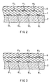
FIG. 2 is a cross-sectional view sectioned along a section line a-a' shown inFIG. 1 . As shown inFIG. 2 , the first right-sidescan connecting wirings active matrix substrate 2. An insulating film (insulating material) 7 is formed on theactive matrix substrate 2, so as to cover the first right-sidescan connecting wirings scan connecting wirings film 7. Further, aprotective film 8 is formed on the insulatingfilm 7, so as to cover the second right-sidescan connecting wirings film 7 is interposed between the first right-sidescan connecting wirings scan connecting wirings - Thus, in the present embodiment, the first right-side
scan connecting wirings scan connecting wirings scan connecting wirings 611 to 617 are formed on a single layer. - Note that in the above, an example was described in which the right-side
scan connecting wirings 611 to 617 are formed on the first layer and the second layer in the stated order from the third side S3 toward the second side S2 at the location of the section line a-a' shown inFIG. 1 , but the present invention is not limited thereto. For example, as shown inFIG. 3 , the right-side scan connecting wirings may be formed on the first layer and the second layer such that the first right-sidescan connecting wirings 611 and the second right-sidescan connecting wirings 612 overlap each other, the first right-sidescan connecting wirings 613 and the second right-sidescan connecting wirings 614 overlap each other, and the first right-sidescan connecting wirings 615 and the second right-sidescan connecting wirings 616 overlap each other. In this case, an even more compact and higher definitionactive matrix substrate 2 can be realized in comparison with the mode shown inFIG. 2 . - Returning to
FIG. 1 , a plurality of first extension wirings 53 respectively extending toward the first side S1 from the plurality ofscan terminals 51 connected to the right-sidescan connecting wirings 611 to 617 are connected to the plurality of thescan terminals 51. Also, a first inspection wiring (seventh inspection wiring) 63 for scan wirings is connected to the plurality offirst extension wirings 53. That is, thefirst inspection wiring 63 for scan wirings is connected to each of the plurality offirst extension wirings 53. Also, afirst inspection pad 64 for scan wirings is further connected to thefirst inspection wiring 63 for scan wirings. Thefirst inspection pad 64 for scan wirings is a pad through which scan inspection signals can be input. Note that scan inspection signals are inspection signals that functions as scan signals. - In the present embodiment, because the
first inspection wiring 63 for scan wirings is connected to each of the plurality offirst extension wirings 53, scan inspection signals can be collectively input to the first scan wirings 401 to 407 from thefirst inspection pad 64 for scan wirings. Also, because thefirst inspection wiring 63 for scan wirings is connected to each of the plurality offirst extension wirings 53, static electricity generated in theactive matrix substrate 2 can be eliminated or dispersed from thefirst inspection wiring 63 for scan wirings and thefirst inspection pad 64 for scan wirings. Because static electricity generated in theactive matrix substrate 2 can be eliminated or dispersed, short circuit or disconnection due to static electricity, as well as changes in TFT or MIM characteristics and the like can be suppressed. - Also, left-side scan connecting wirings (first connectinng wirings) 651 to 656 respectively connecting the
scan terminals 51 and the input ends 441 to 446 for scan signals provided at the opposite end of the second scan wirings 411 to 416 are formed in theperipheral wiring region 6. That is, the left-sidescan connecting wirings 651 to 656 are extracted from the input ends 441 to 446 for scan signals toward the second side S2, formed in theperipheral wiring region 6 along the second side S2, and connected to thescan terminals 51. - Here, the left-side
scan connecting wirings 651 to 656 include first left-side scan connecting wirings (third connecting wirings, sixth connecting wirings) 651, 653 and 655, and second left-side scan connecting wirings (fourth connecting wirings, eighth connecting wirings) 652, 654 and 656. The first left-sidescan connecting wirings scan connecting wirings - Here, the second left-side
scan connecting wirings portions scan connecting wirings scan connecting wirings portions portions scan terminals 51 are formed on the second layed That is, wirings formed on the first layer are electrically connected at the connectingportions portions scan connecting wirings - A plurality of second extension wirings 54 respectively extending from the plurality of the
scan terminals 51 connected to the left-sidescan connecting wirings 64 toward the first side S1 are connected to the plurality of thescan terminals 51. Also, a second inspection wiring (eighth inspection wiring) 67 for scan wirings is connected to the plurality ofsecond extension wirings 54. That is, the second inspection wiring 67 for scan wirings is connected to each of the plurality ofsecond extension wirings 54. Also, asecond inspection pad 68 for scan wirings is further connected to the second inspection wiring 67 for scan wirings. Thesecond inspection pad 68 for scan wirings is a pad through which scan inspection signals can be input. - In the present embodiment, because the second inspection wiring 67 for scan wirings is connected to each of the plurality of second extension wirings 54, scan inspection signals can be collectively input to the second scan wirings 411 to 416 from the
second inspection pad 68 for scan wirings. Also, because the second inspection wiring 67 for scan wirings is connected to each of the plurality of second extension wirings 54, static electricity generated in theactive matrix substrate 2 can be eliminated or dispersed from the second inspection wiring 67 for scan wirings and thesecond inspection pad 68 for scan wirings. - Also, right-side
scan switching elements 691 to 697 respectively connected to the right-sidescan connecting wirings 611 to 617 are formed in theperipheral wiring region 6. Specifically, the right-sidescan switching elements 691 to 697 are formed in theperipheral wiring region 6 in proximity to the input ends 431 to 437 for scan signals. Here, the right-sidescan switching elements 691 to 697 include first right-side scan switching elements (first switching elements, third switching elements) 691, 693, 695 and 697 respectively connected to the first right-sidescan connecting wirings scan connecting wirings - Here, a first inspection wiring (first inspection wiring, third inspection wiring) 70 for right-side scan connecting wirings is further connected to the first right-side
scan switching element 691, the second right-sidescan switching element 694 and the first right-sidescan switching element 695. That is, thefirst inspection wiring 70 for right-side scan connecting wirings is an inspection wiring capable of inputting scan inspection signals to the non-adjacent first right-sidescan switching elements scan switching elements scan switching element 694 among the second right-sidescan switching elements first inspection wiring 70 for right-side scan connecting wirings is formed in theperipheral wiring region 6 so as to intersect each of the right-sidescan connecting wirings 611 to 617. - Also, a
first inspection pad 71 for right-side scan connecting wirings is further connected to thefirst inspection wiring 70 for right-side scan connecting wirings. Thefirst inspection pad 71 for right-side scan connecting wirings is a pad through which scan inspection signals can be input. Scan inspection signals can thereby be input to the first right-sidescan connecting wirings 611, the second right-sidescan connecting wirings 614 and the first right-sidescan connecting wirings 615 from thefirst inspection pad 71 for right-side scan connecting wirings. - Also, a second inspection wiring (second inspection wiring, fifth inspection wiring) 72 for right-side scan connecting wirings is further connected to the second right-side
scan switching element 692, the first right-sidescan switching element 693, the second right-sidescan switching element 696 and the first right-sidescan switching element 697. That is, the second inspection wiring 72 for right-side scan connecting wirings is an inspection wiring capable of inputting scan inspection signals to the non-adjacent first right-sidescan switching elements first inspection wiring 70 for right-side scan connecting wirings among the first right-sidescan switching elements scan switching elements first inspection wiring 70 for right-side scan connecting wirings among the second right-sidescan switching elements peripheral wiring region 6 so as to intersect each of the right-sidescan connecting wirings 611 to 617. - Also, a
second inspection pad 73 for right-side scan connecting wirings is further connected to the second inspection wiring 72 for right-side scan connecting wirings. Thesecond inspection pad 73 for right-side scan connecting wirings is a pad through which scan inspection signals can be input. Scan inspection signal can thereby be input to the second right-sidescan connecting wiring 612, the first right-sidescan connecting wiring 613, the second right-sidescan connecting wiring 616 and the first right-sidescan connecting wiring 617 from thesecond inspection pad 73 for right-side scan connecting wirings. - That is, because the
first inspection wiring 70 for right-side scan connecting wirings, thefirst inspection pad 71 for right-side scan connecting wirings, the second inspection wiring 72 for right-side scan connecting wirings and thesecond inspection pad 73 for right-side scan connecting wirings are formed as described above in theperipheral wiring region 6, different scan inspection signals can be input to each of the adjacent first right-sidescan connecting wirings scan connecting wirings scan connecting wirings scan connecting wirings - Also, left-side
scan switching elements 741 to 746 respectively connected to the left-sidescan connecting wirings 651 to 656 are formed in theperipheral wiring region 6. Specifically, the left-sidescan switching elements 741 to 746 are formed in theperipheral wiring region 6 in proximity to the input ends 441 to 446 for scan signals. Here, the left-sidescan switching elements 741 to 746 include first left-side scan switching elements (first switching elements, fourth switching elements) 741, 743 and 745 respectively connected to the first left-sidescan connecting wirings scan connecting wirings - Here, a first inspection wiring (first inspection wiring, fourth inspection wiring) 75 for left-side scan connecting wirings is further connected to the first left-side
scan switching element 741, the second left-sidescan switching element 744 and the first left-sidescan switching element 745. That is, thefirst inspection wiring 75 for left-side scan connecting wirings is an inspection wiring capable of inputting scan inspection signals to the non-adjacent first left-sidescan switching element scan switching elements scan switching element 744 among the second left-sidescan switching elements first inspection wiring 75 for left-side scan connecting wirings is formed in theperipheral wiring region 6 so as to intersect each of the left-sidescan connecting wirings 651 to 656. - Also, a
first inspection pad 76 for left-side scan connecting wirings is further connected to thefirst inspection wiring 75 for left-side scan connecting wirings. Thefirst inspection pad 76 for left-side scan connecting wirings is a pad through which scan inspection signals can be input. Scan inspection signals can thereby be input to the first left-sidescan connecting wirings 651, the second left-sidescan connecting wirings 654 and the first left-sidescan connecting wirings 655 from thefirst inspection pad 76 for left-side scan connecting wirings. - Also, a second inspection wiring (second inspection wiring, sixth inspection wiring) 77 for left-side scan connecting wirings is further connected to the second left-side
scan switching element 742, the first left-sidescan switching element 743 and the second left-sidescan switching element 746. That is, the second inspection wiring 77 for left-side scan connecting wirings is an inspection wiring capable of inputting scan inspection signals to the non-adjacent first left-sidescan switching element 743 that is not connected to thefirst inspection wiring 75 for left-side scan connecting wirings among the first left-sidescan switching elements scan switching element first inspection wiring 75 for left-side scan connecting wirings among the second left-sidescan switching elements peripheral wiring region 6 so as to intersect each of the left-sidescan connecting wirings 651 to 656. - Also, a
second inspection pad 78 for left-side scan connecting wirings is further connected to the second inspection wiring 77 for left-side scan connecting wirings. Thesecond inspection pad 78 for left-side scan connecting wirings is a pad through which scan inspection signals can be input. Scan inspection signals can thereby be input to the second left-sidescan connecting wiring 652, the first left-sidescan connecting wiring 653 and the second left-sidescan connecting wiring 616 from thesecond inspection pad 78 for left-side scan connecting wirings. - That is, because the
first inspection wiring 75 for left-side scan connecting wirings, thefirst inspection pad 76 for left-side scan connecting wirings, the second inspection wiring 77 for left-side scan connecting wirings and thesecond inspection pad 78 for left-side scan connecting wirings are formed as described above in theperipheral wiring region 6, different scan inspection signals can be input to each of the adjacent first left-sidescan connecting wirings scan connecting wirings scan connecting wirings scan connecting wirings - Here, the
first inspection wiring 70 for right-side scan connecting wirings and the second inspection wiring 72 for right-side scan connecting wirings are formed, as described above, in theperipheral wiring region 6 so as to intersect each of the right-sidescan connecting wirings 611 to 617. Also, thefirst inspection wiring 75 for left-side scan connecting wirings and the second inspection wiring 77 for left-side scan connecting wirings are formed, as described above, in theperipheral wiring region 6 so as to intersect each of the left-sidescan connecting wirings 651 to 656. Because the right-sidescan connecting wirings 611 to 617 and the left-sidescan connecting wirings 651 to 656 both intersect the same number of inspection wirings, the load on the right-sidescan connecting wirings 611 to 617 and the load on the left-sidescan connecting wirings 651 to 656 are equal. The carrying potential of the first scan wirings 401 to 407 connected to the right-sidescan connecting wirings 611 to 617 and the carrying potential of the second scan wirings 411 to 416 connected to the left-sidescan connecting wirings 651 to 656 will thus be the same. Thus, in the case where theactive matrix substrate 2 according to the present embodiment is incorporated in a display device, an image with uniform brightness will be displayed on the display screen of the display device. - Also, a storage capacitor
main wiring 79 is formed in theperipheral wiring region 6 so as to be closer to thedisplay region 4 than are the inspection wirings 70, 72, 75 and 77. The storage capacitormain wiring 79 is formed in theperipheral wiring region 6 along the second side S2 and the third side S3, so as to sandwich thedisplay region 4 from the left and right. A storage capacitor wiring (not shown) formed in thedisplay region 4 is connected to the storage capacitormain wiring 79. Also, aninspection pad 80 for storage capacitor wirings is further connected to the storage capacitormain wiring 79 via theterminal arrangement region 5. Theinspection pad 80 for storage capacitor wirings is a pad through which storage capacitor inspection signals can be input. Storage capacitor inspection signals can thereby be input to the storage capacitor wirings frominspection pad 80 for storage capacitor wirings. Note that the storage capacitor inspection signals are inspection signals for detecting disconnection of the storage capacitor wirings and leakage to the scan wirings 40 and 41. - Incidentally, in the present embodiment, the right-side
scan switching elements 691 to 697 are formed in theperipheral wiring region 6 in proximity to the input ends 431 to 437 for scan signals and the left-sidescan switching elements 741 to 746 are formed in theperipheral wiring region 6 in proximity to the input ends 441 to 446 for scan signals, as discussed above. Here, let us hypothetically consider the case where, conversely, the right-sidescan switching elements 691 to 697 are formed in theperipheral wiring region 6 in proximity to the terminal ends for scan signals (i.e., opposite end of first scan wirings 401 to 407), and the left-sidescan switching elements 741 to 746 are formed in theperipheral wiring region 6 in proximity to the terminal ends for scan signals (i.e., one end of second scan wirings 411 to 416). -
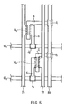
FIG. 4 is a plan view showing a schematic configuration of a liquid crystal panel 1a in the case where the right-sidescan switching elements 691 to 697 and the left-sidescan switching elements 741 to 746 are formed in theperipheral wiring region 6 close to the terminal ends for scan signals. Note that inFIG. 4 , reference numerals are only attached to principal members, in order to simplify the description. As shown inFIG. 4 , because the right-sidescan switching elements 691 to 697 are formed in theperipheral wiring region 6 close to the terminal ends for scan signals,first extraction wirings 40a extracted from the opposite side of the first scan wirings 401 to 407 toward the second side S2 are newly formed in theperipheral wiring region 6. That is, thefirst extraction wirings 40a connect the right-sidescan switching elements 691 to 697 and the opposite ends of the first scan wirings 401 to 407. Also, because the left-sidescan switching elements 741 to 746 are formed in theperipheral wiring region 6 close to the terminal ends for scan signals,second extraction wirings 41a extracted from the opposite side of the second scan wirings 411 to 416 toward the third side S3 are newly formed in theperipheral wiring region 6. In other words, thesecond extraction wirings 41a connect the left-sidescan switching elements 741 to 746 and the opposite ends of the second scan wirings 411 to 416. - That is, the storage capacitor
main wiring 79 and thefirst extraction wirings 40a intersect in a portion D1 shown inFIG. 4 . Because the storage capacitormain wiring 79 and thefirst extraction wirings 40a intersect, a significant load is placed on the first scan wirings 401 to 407. Also, the storage capacitormain wiring 79 and thesecond extraction wirings 41a intersect in a portion D2 shown inFIG. 4 . Because the storage capacitormain wiring 79 and thesecond extraction wirings 41a intersect, a significant load is placed on the second scan wirings 411 to 416. In other words, because a significant load is placed on the scan wirings 40 and 41, scan signals input to the scan wirings 40 and 41 are delayed Because the scan signals are delayed, it is difficult to charge data signals from the data wirings 42 in the storage capacitor. As a result, in the case where the liquid crystal panel 1a shown inFIG. 4 is incorporated in an electronic device, images that do not achieve the desired brightness, for example, are displayed on the display screen of the electronic device. In other words, the display quality of the liquid crystal panel 1a decreases. - In contrast, with the
liquid crystal panel 1 according to the present embodiment, because the right-sidescan switching elements 691 to 697 and the left-sidescan switching elements 741 to 746 are formed in theperipheral wiring region 6 in proximity to the input ends for scan signals, as shown inFIG. 1 , the abovefirst extraction wirings 40a andsecond extraction wirings 41a need not be formed in theperipheral wiring region 6. There is thus no intersection between the storage capacitormain wiring 79 andfirst extraction wirings 40a or between the storage capacitormain wiring 79 andsecond extraction wirings 41a. As a result, problems such as discussed above do not occur with theliquid crystal panel 1 according to the present embodiment. - Also, with the liquid crystal panel 1a shown in
FIG. 4 , because thefirst extraction wirings 40a are newly formed in theperipheral wiring region 6, short circuits more readily occur between thefirst extraction wirings 40a and the left-sidescan connecting wirings 651 to 656. Also, because thesecond extraction wirings 41a are newly formed in theperipheral wiring region 6, short circuits more readily occur between thesecond extraction wirings 41a and the right-sidescan connecting wirings 611 to 617. Further, because thefirst extraction wirings 40a and thesecond extraction wirings 41a are newly formed in theperipheral wiring region 6, space for forming other wirings and switching elements in theperipheral wiring region 6 is reduced. Thus, short-circuit failures of the wirings and switching elements increase. - In contrast, with the
liquid crystal panel 1 according to the present embodiment, because the right-sidescan switching elements 691 to 697 and the left-sidescan switching elements 741 to 746 are, as shown inFIG. 1 , formed in theperipheral wiring region 6 in proximity to the input ends for scan signals, the abovefirst extraction wirings 40a andsecond extraction wirings 41a need not be formed in theperipheral wiring region 6. As a result, problems such as discussed above do not occur with theliquid crystal panel 1 according to the present embodiment. - From the above, the mode in which the right-side
scan switching elements 691 to 697 and the left-sidescan switching elements 741 to 746 are formed in theperipheral wiring region 6 in proximity to the input ends for scan signals (seeFIG. 1 ) is preferable to the mode in which the right-sidescan switching elements 691 to 697 and the left-sidescan switching elements 741 to 746 are formed in theperipheral wiring region 6 close to the terminal ends for scan signals (seeFIG. 4 ). That is, theliquid crystal panel 1 shown inFIG. 1 increases yield as well as increasing display quality, in comparison with the liquid crystal panel 1a shown inFIG. 4 . - Returning to
FIG. 1 , data connecting wirings (second connecting wirings) 811, 812, 813, ...81i respectively connecting thedata terminals 52 and the input ends 451, 452, 453, ...45i for data signals provided at one end of the data wirings 421, 422, 423, ...42i are formed in theperipheral wiring region 6. That is, thedata connecting wirings 81 are extracted from the input ends 44 for data signals toward the first side S1, and connected to thedata terminals 52. Note that inFIG. 1 , thedata connecting wirings - Also, switching elements (seventh switching elements) 821, 822, 823, ...82i for data wirings connected to the opposite ends of the data wirings 421, 422, 423, ...42i are formed in the
peripheral wiring region 6. Note that inFIG. 1 , the switchingelements - Here, a first inspection wiring (ninth inspection wiring) 83 for data wirings is further connected to the
switching elements first inspection wiring 83 for data wirings is an inspection wiring capable of inputting data inspection signals to thenon-adjacent switching elements elements 82 for data wirings. Note that thefirst inspection wiring 83 for data wirings is formed in theperipheral wiring region 6 on the fourth side S4 and the second side S2. Also, afirst inspection pad 84 for data wirings is further connected to thefirst inspection wiring 83 for data wirings. Thefirst inspection pad 84 for data wirings is a pad through which data inspection signals can be input. Note that data inspection signals are inspection signals that functions as data signals. Data inspection signals can thereby be input to the data wirings 421, 424, 427, ...42i-2 from thefirst inspection pad 84 for data wirings. - Also, a second inspection wiring (tenth inspection wiring) 85 for data wirings is further connected to the
switching elements non-adjacent switching elements first inspection wiring 83 for data wirings among the switchingelements 82 for data wirings. Note that the second inspection wiring 85 for data wirings is formed in theperipheral wiring region 6 on the fourth side S4 and the second side S2, similarly to thefirst inspection wiring 83 for data wirings. Also, asecond inspection pad 86 for data wirings is further connected to the second inspection wiring 85 for data wirings. Thesecond inspection pad 86 for data wirings is a pad through which data inspection signals can be input. Data inspection signals can thereby be input to the data wirings 422, 425, 428, ...42i-1 from thesecond inspection pad 86 for data wirings. - Further, a third inspection wiring (tenth inspection wiring) 87 for data wirings is further connected to the
switching elements third inspection wiring 87 for data wirings is an inspection wiring capable of inputting data inspection signals to thenon-adjacent switching elements first inspection wiring 83 for data wirings or the second inspection wiring 85 for data wirings among the switchingelements 82 for data wirings. Note that thethird inspection wiring 87 for data wirings is formed in theperipheral wiring region 6 on the fourth side S4 and the second side S2, similarly to thefirst inspection wiring 83 for data wirings and the second inspection wiring 85 for data wirings. Athird inspection pad 88 for data wirings is further connected to thethird inspection wiring 87 for data wirings. Thethird inspection pad 88 for data wirings is a pad through which data inspection signals can be input. Data inspection signals can thereby be input to the data wirings 423, 426, 429, ...42i from thethird inspection pad 88 for data wirings. - That is, because the
first inspection wiring 83 for data wirings, thefirst inspection pad 84 for data wirings, the second inspection wiring 85 for data wirings, thesecond inspection pad 86 for data wirings, thethird inspection wiring 87 for data wirings and thethird inspection pad 88 for data wirings are formed as described above in theperipheral wiring region 6, different data inspection signals can be input to each of the adjacent data wirings 42 and the adjacentdata connecting wirings 81. Short circuits of the data wirings 42 and thedata connecting wirings 81 can thereby be detected. - Further, a switching element control wiring (first control wiring, second control wiring) 89 connected to the right-side
scan switching elements 691 to 697, the left-sidescan switching elements 741 to 746 and theswitching elements peripheral wiring region 6. The switchingelement control wiring 89 is formed closer to thedisplay region 4 than are thefirst inspection wiring 70 for right-side scan connecting wirings, the second inspection wiring 72 for right-side scan connecting wirings, thefirst inspection wiring 75 for left-side scan connecting wirings and the second inspection wiring 77 for left-side scan connecting wirings. Acontrol pad 90 is connected to the switchingelement control wiring 89. Thecontrol pad 90 is a pad through which control signals for turning switching elements on/off can be input. Control signals can thereby be input to the right-sidescan switching elements 691 to 697, the left-sidescan switching elements 741 to 746 and theswitching elements control pad 90. - Incidentally, in the present embodiment, as shown in
FIG. 1 , thefirst inspection wiring 70 for right-side scan connecting wirings and the second inspection wiring 72 for right-side scan connecting wirings are adjacent to each other, and all of the right-sidescan switching elements 691 to 697 are formed between thefirst inspection wiring 70 for right-side scan connecting wirings and the second inspection wiring 72 for right-side scan connecting wirings. Also, thefirst inspection wiring 75 for left-side scan connecting wirings and the second inspection wiring 77 for left-side scan connecting wirings are adjacent to each other, and all of the left-sidescan switching elements 741 to 746 are formed between thefirst inspection wiring 75 for left-side scan connecting wirings and the second inspection wiring 77 for left-side scan connecting wirings. This enables the number of connecting portions for electrically connecting wirings formed on the first layer and wirings formed on the second layer to be reduced, as will be discussed in detail below. In other words, when connecting portions are formed, wirings formed on the first layer and wirings formed on the second layer can lose electrical continuity due to faulty connecting portions or the like. Resistance is also increased by the connecting portions. Scanning wirings 40 and 41 cannot be correctly inspected in such cases. Further, the size of theactive matrix substrate 2 increases, together with an increased likelihood of short circuits with adjacent wirings, since space for forming the connecting portions is needed. Thus, as few connecting portions as possible is preferable. -
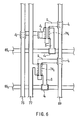
FIG. 5 is an illustrative diagram showing an enlarged view of an E portion shown inFIG. 1 . Note that inFIG. 5 , the insulatingfilm 7 and theprotective film 8 are omitted for ease of description. Here, a arrangement relationship of thefirst inspection wiring 75 for left-side scan connecting wirings, the second inspection wiring 77 for left-side scan connecting wirings, the switchingelement control wiring 89 and the left-sidescan switching elements 741 to 746 will now be described, focusing on the location shown inFIG. 5 . Note that because a arrangement relationship of thefirst inspection wiring 70 for right-side scan connecting wirings, the second inspection wiring 72 for right-side scan connecting wirings, the switchingelement control wiring 89 and the right-sidescan switching elements 691 to 697 is similar to the aforementioned arrangement relationship, detailed description thereof will be omitted here. - In the present embodiment, the
first inspection wiring 75 for left-side scan connecting wirings, the second inspection wiring 77 for left-side scan connecting wirings and the switchingelement control wiring 89 are formed on the second layer. The first left-sidescan connecting wirings scan connecting wirings portions scan switching elements 741 to 746 are formed on the first layer. Source electrodes S and drain electrodes D of the left-sidescan switching elements 741 to 746 are formed on the second layer. - In such cases, as shown in
FIG. 5 , a connecting portion J1 for electrically connecting the switchingelement control wiring 89 and the gate electrode G of the first left-sidescan switching element 741 will be required. A connecting portion J2 for electrically connecting the left-sidescan connecting wiring 651 and the source electrode S of the first left-sidescan switching element 741 will also be required. Similarly, a connecting portion J3 for electrically connecting the switchingelement control wiring 89 and the gate electrode G of the second left-sidescan switching element 742, and a connecting portion J4 for electrically connecting the left-sidescan connecting wiring 652 and the source electrode S of the second left-sidescan switching element 742 will be required. That is, in the case of forming the first left-sidescan switching element 741 and the second left-sidescan switching element 742 in theperipheral wiring region 6, the four connecting portions J1 to J4 will be required as connecting elements for electrically connecting wirings formed on the first layer with wirings formed on the second layer. - Here, let us hypothetically consider the case where all of the left-side
scan switching elements 741 to 746 are formed between the second inspection wiring 77 for left-side scan connecting wirings and the switchingelement control wiring 89. In this case, there will be six connecting portions J1 to J6, as shown inFIG. 6 . Again, let us hypothetically consider the case where all of the left-sidescan switching elements 741 to 746 are formed closer to thedisplay region 4 than are thefirst inspection wiring 75 for left-side scan connecting wirings, the second inspection wiring 77 for left-side scan connecting wirings and the switchingelement control wiring 89. In this case, there will be eight connecting portions J1 to J8, as shown inFIG. 7 . - From the above, the number of connecting portions can, as shown in the present embodiment, be reduced in comparison with the above modes (
FIGS. 6 and7 ), by forming all of the right-sidescan switching elements 691 to 697 between thefirst inspection wiring 70 for right-side scan connecting wirings and the second inspection wiring 72 for right-side scan connecting wirings, and forming all of the left-sidescan switching elements 741 to 746 between thefirst inspection wiring 75 for left-side scan connecting wirings and the second inspection wiring 77 for left-side scan connecting wirings. As a result, theactive matrix substrate 2 according to the present embodiment can be reduced in size as well as being able to contribute to improving the yield of theliquid crystal panel 1. - Note that the number of connecting portions can also be reduced, similarly to the case shown in
FIG. 5 , with a mode in which the left-side scan switching elements connected to thefirst inspection wiring 75 for left-side scan connecting wirings are formed between thefirst inspection wiring 75 for left-side scan connecting wirings and the switchingelement control wiring 89, and the left-side scan switching elements connected to the second inspection wiring 77 for left-side scan connecting wirings are formed between the second inspection wiring 77 for left-side scan connecting wirings and the switchingelement control wiring 89. That is, as shown inFIG. 8 , the first left-sidescan switching element 741 is formed on the left side of the switchingelement control wiring 89, and the second left-sidescan switching element 742 is formed on the right side of the switchingelement control wiring 89. In this case, the four connecting portions J1 to J4 will be required, similarly to the case shownFIG. 5 . - The number of connecting portions can also be reduced, similarly to the case shown in
FIG. 5 , with a mode in which the left-side scan switching elements connected to thefirst inspection wiring 75 for left-side scan connecting wirings are formed on the left side of thefirst inspection wiring 75 for left-side scan connecting wirings and the switchingelement control wiring 89, and the left-side scan switching elements connected to the second inspection wiring 77 for left-side scan connecting wirings are formed on the right side of the second inspection wiring 77 for left-side scan connecting wirings and the switchingelement control wiring 89. That is, as shown inFIG. 9 , the first left-sidescan switching element 741 is formed on the left side of thefirst inspection wiring 75 for left-side scan connecting wirings and the switchingelement control wiring 89, and the second left-sidescan switching element 742 is formed on the right side of the second inspection wiring 77 for left-side scan connecting wirings and the switchingelement control wiring 89. In this case, the four connecting portions J1 to J4 will be required, similarly to the case shownFIG. 5 . - Returning to
FIG. 1 , acommon inspection wiring 91 is formed in theperipheral wiring region 6 on the second side S2. Acommon electrode pad 92 is connected to thecommon inspection wiring 91. Atransfer pad 93 is further connected to thecommon inspection wiring 91. Thetransfer pad 93 is connected to a common electrode (not shown) formed on the opposingsubstrate 3. Acommon voltage can thereby be applied to the common electrode formed on the opposingsubstrate 3 from thecommon electrode pad 92. - Next, a method for manufacturing the
liquid crystal panel 1 according to the present embodiment will be described. Note that, hereinafter, an inspection process of inspecting the electrical connection state of theliquid crystal panel 1 will, in particular, be described in detail. - That is, thin films such as a conductive film, an insulating film, a protective film and an orientation film are laminated on a transparent glass substrate to manufacture a base substrate for active matrix substrates on which are formed a plurality of active matrix substrate regions to be cut out as
active matrix substrates 2. Also, thin films such as a black matrix, color filters, a conductive film and an orientation film are laminated on a transparent glass substrate to manufacture a base substrate for opposing substrates on which are formed a plurality of opposing substrate regions to be cut out as opposingsubstrates 3. A sealant is applied to one of the two base substrates. The two base substrates are then adhered together after the sealant has been applied The two base substrates adhered together are then sectioned as mother substrates from which a prescribed number ofliquid crystal panels 1 having anactive matrix substrate 2 and an opposingsubstrate 3 are formed. Aliquid crystal material is injected into each of theliquid crystal panel 1 sectioned as mother substrates using a vacuum injection method, for example, through an inlet formed between theactive matrix substrate 2 and the opposingsubstrate 3. Note that the liquid crystal material may be injected using a drop injection method rather than a vacuum injection method. In this case, neither the inlet nor a process of sealing the inlet portion is required. Theliquid crystal panel 1 shown inFIG. 1 is a single liquid crystal panel that has been sectioned as a mother substrate and injected with a liquid crystal material. Accordingly, although illustration thereof has been omitted, other liquid crystal panels exist above, below and to the left and right of theliquid crystal panel 1 shown inFIG. 1 . - An inspection process of inspecting the electrical connection state of the
liquid crystal panel 1 is then performed, prior to attaching the driver in theterminal arrangement region 5. That is, the inspection process is for inspecting for disconnection or short circuit of wiring and for picture element defects in theactive matrix substrate 2 of theliquid crystal panel 1. Also, the inspection process may be divided into a first inspection process and a second inspection process, as will be discussed in detail later. - As for the inspection method, in the first inspection process, an inspection probe is brought into contact with the
first inspection pad 64 for scan wirings, thesecond inspection pad 68 for scan wirings, theinspection pad 80 for storage capacitor wirings, thefirst inspection pad 84 for data wirings, thesecond inspection pad 86 for data wirings, thethird inspection pad 88 for data wirings, thecontrol pad 90 and thecommon electrode pad 92, and a voltage is applied to the pads, for example. In the second inspection process, an inspection probe is brought into contact with thefirst inspection pad 71 for right-side scan connecting wirings, thesecond inspection pad 73 for right-side scan connecting wirings, thefirst inspection pad 76 for left-side scan connecting wirings, thesecond inspection pad 78 for left-side scan connecting wirings, theinspection pad 80 for storage capacitor wirings, thefirst inspection pad 84 for data wirings, thesecond inspection pad 86 for data wirings, thethird inspection pad 88 for data wirings, thecontrol pad 90 and thecommon electrode pad 92, and a voltage is applied to the pads, for example. Note that the order in which the inspection probe is brought into contact with the pads is not particularly limited here. - Scan inspection signals that function as scan signals are thereby input to the scan wirings 40 and 41. Here, the scan inspection signals are, for example, signals that switch on the switching element of each picture element for at least a fixed period. Also, data inspection signals that function as data signals are input to the data wirings 42. Here, the data inspection signals are, for example, signals that orient the liquid crystal in each picture element region in a prescribed direction. When the molecular orientation direction of liquid crystal is controlled as a result of a data signal being applied to each picture element electrode with the switching element of each picture element in an ON state, and the
liquid crystal panel 1 is irradiated from the back surface thereof with irradiation means such as a backlight, for example, an image will be displayed on the display screen of theliquid crystal panel 1 corresponding to thedisplay region 4 of the active matrix substrate 2 (hereinafter, "display screen of theliquid crystal panel 1"). Accordingly, inspection can be made for disconnection and short circuit of wiring in theactive matrix substrate 2 of theliquid crystal panel 1 by an inspector visually inspecting the display screen of theliquid crystal panel 1. Note that an image recognition device may be used instead of or in addition to visual inspection by an inspector, or inspection may be performed using a detection device or the like that electrically detects disconnection or short circuit of wiring. - Here, the first inspection process will be discussed in detail.
- Hereinafter, first, the method for detecting disconnection of the scan wirings 40 and 41, the right-side
scan connecting wirings 611 to 617 and the left-sidescan connecting wirings 651 to 656 will be described. - That is, a data inspection signal is input to the data wirings 42, and scan inspection signals are input to the scan wirings 40 and 41, the right-side
scan connecting wirings 611 to 617 and the left-sidescan connecting wirings 651 to 656 from thefirst inspection pad 64 for scan wirings and thesecond inspection pad 68 for scan wirings. In the case where the scan wirings 40 and 41 are disconnected, picture elements in lines corresponding to scan wirings 40 and 41 at and after the location of the disconnection will thus not be displayed on the display screen of theliquid crystal panel 1. Thus, the inspector is able to detect that the scan wirings 40 and 41 are disconnected. - Also, in the case where the right-side
scan connecting wirings 611 to 617 are disconnected, all of the lines corresponding to the first scan wirings 401 to 407 connected to the disconnected right-sidescan connecting wirings 611 to 617 will not be displayed on the display screen of theliquid crystal panel 1. Thus, the inspector is able to detect that the right-sidescan connecting wirings 611 to 617 are disconnected. Further, in the case where the left-sidescan connecting wirings 651 to 656 are disconnected, all of the lines corresponding to the second scan wirings 411 to 416 connected to the disconnected left-sidescan connecting wirings 651 to 656 will not be displayed on the display screen of theliquid crystal panel 1. Thus, the inspector is able to detect that the left-sidescan connecting wirings 651 to 656 are disconnected. - Next, the method for detecting a short circuit between the scan wirings 40 and 41 will be described.
- That is, a scan inspection signal is input to the first scan wirings 401 to 407 from the
first inspection pad 64 for scan wirings, without inputting a scan inspection signal to the second scan wirings 411 to 416. In the case where the first scan wirings 401 to 407 and the second scan wirings 411 to 416 are short circuited at this time, not only the lines corresponding to the first scan wirings 401 to 407 but also lines corresponding to the second scan wirings 411 to 416 will be displayed on the display screen of theliquid crystal panel 1. Thus, the inspector is able to detect that there is a short circuit between the first scan wirings 401 to 407 and the second scan wirings 411 to 416. Note that a scan inspection signal may be input to the second scan wirings 411 to 416 from thesecond inspection pad 68 for scan wirings, without inputting a scan inspection signal to the first scan wirings 401 to 407. - Incidentally, in the above, scan inspection signals are collectively input to the right-side
scan connecting wirings 611 to 617 from thefirst inspection pad 64 for scan wirings. That is, the same scan inspection signal is input to each of the adjacent first right-sidescan connecting wirings scan connecting wirings scan connecting wirings scan connecting wirings scan connecting wirings scan connecting wirings - Similarly, in the above first inspection process, short circuits between adjacent first left-side
scan connecting wirings scan connecting wirings - Next, the method for detecting disconnection of the data wirings 42 will be described.
- That is, scan inspection signals are input to the scan wirings 40 and 41, and data inspection signals are input to the data wirings 42 from the
first inspection pad 84 for data wirings, thesecond inspection pad 86 for data wirings and thethird inspection pad 88 for data wirings. In the case where data wirings 42 are disconnected, picture elements in lines corresponding to data wirings 42 at and after the location of the disconnection are displayed differently to picture elements in normal lines. Thus, the inspector is able to detect that data wirings 42 are disconnected. - Next, the method for detecting a short circuit between the data wirings 42 and the
data connecting wirings 81 will be described - That is, a control signal for turning on the
switching elements 82 for data wirings is input to theswitching elements 82 for data wirings from thecontrol pad 90. The switchingelements 82 for data wirings are thereby turned on. Here, a data inspection signal is, for example, input to only the data wirings 421, 424, 427, ...42i-2 among the plurality of data wirings 42, and a data inspection signal is not input to the data wirings 422, 423, 425, ...42i-1, 42i other than the data wirings 421, 424, 427, ... 42i-2. The inspection probe is, for example, brought into contact with only thefirst inspection pad 84 for data wirings, and is not brought into contact with thesecond inspection pad 86 for data wirings or thethird inspection pad 88 for data wirings. - In the case where the data wrings 421, 424, 427, ...42i-2 are short circuited, this results in not only the lines corresponding to the data wirings 421, 424, 427, ...42i-2 but also lines corresponding to short-circuited data wirings also being displayed. Thus, the inspector is able to detect that the data wirings 421, 424, 427, ...42i-2 are short circuited. Also, in the case where the
data connecting wirings data connecting wirings data connecting wirings - Similarly, when the inspection probe is brought into contact with only the
second inspection pad 86 for data wirings, and is not brought into contact with thefirst inspection pad 84 for data wirings or thethird inspection pad 88 for data wirings, the inspector is able to detect a short circuit of the data wirings 422, 425, 428, ...42i-1 and thedata connecting wirings third inspection pad 88 for data wirings, and is not brought into contact with thefirst inspection pad 84 for data wirings or thesecond inspection pad 86 for data wirings, the inspector is able to detect a short circuit of the data wirings 423, 426, 429, ...42i and thedata connecting wirings - As described above, in the first inspection process, short circuits of the right-side
scan connecting wirings 611 to 617 and the left-sidescan connecting wirings 651 to 656 thus cannot be detected. In order to inspect for the presence of short circuits of the right-sidescan connecting wirings 611 to 617 and the left-sidescan connecting wirings 651 to 656, the second inspection process is subsequently performed. - Here, a cutting off process of cutting off the
first extension wirings 53 and the second extension wirings 54 is performed before the second inspection process. Specifically, thefirst extension wirings 53 and the second extension wirings 54 are cut off along a cut line C shown inFIG. 1 , for example. As for the cutting off method, cutting off is performed using a laser. Thescan terminals 51 connected to the right-sidescan connecting wirings 611 to 617 are thereby electrically cut off from each other. Thescan terminals 51 connected to the left-sidescan connecting wirings 651 to 656 are also electrically cut off from each other. Note that cutting off may be performed along another cutline instead of the cutline C, provided the plurality ofscan terminals 51 are electrically cut off from each other. - Next, the second inspection process will be discussed in detail.
- Hereinafter, the method for detecting short circuits of the right-side
scan connecting wirings 611 to 617 and the left-sidescan connecting wirings 651 to 656 will be described. Note that since the method for detecting short circuits of the scan wirings 40 and 41, the method for detecting disconnection of the data wirings 42 and the method for detecting short circuits of thedata connecting wirings 81 are similar to the methods described in relation to the first inspection process, detailed description thereof will be omitted here. Also, the method for detecting disconnection of the scan wirings 40 and 41 can be implemented similarly to the first inspection process by using thefirst inspection pad 71 for right-side scan connecting wirings, thesecond inspection pad 73 for right-side scan connecting wirings, thefirst inspection pad 76 for left-side scan connecting wirings and thesecond inspection pad 78 for left-side scan connecting wirings, instead of thefirst inspection pad 64 for scan wirings and thesecond inspection pad 68 for scan wirings used in the first inspection process. - That is, a control signal for turning on the right-side
scan switching elements 691 to 697 is input to the right-sidescan switching elements 691 to 697 from thecontrol pad 90. The right-sidescan switching elements 691 to 697 are thereby turned on. Here, for example, a scan inspection signal is input to only the first right-sidescan connecting wirings scan connecting wirings scan connecting wirings scan connecting wirings scan connecting wiring 614 among the second right-sidescan connecting wirings scan connecting wirings scan connecting wirings 614- The inspection probe is, for example, brought into contact with only thefirst inspection pad 71 for right-side scan connecting wirings, and is not brought into contact with thesecond inspection pad 73 for right-side scan connecting wirings. - In the case where the first right-side
scan connecting wirings scan connecting wirings scan connecting wirings scan connecting wiring 614 formed on the second layer is short circuited, not only the line corresponding to the first scan wiring 404 connected to the second right-sidescan connecting wiring 614 but also lines corresponding to first scan wirings connected to short-circuited second right-side scan connecting wirings will be displayed. Thus, the inspector is able to detect that the second right-sidescan connecting wiring 614 formed on the second layer is short circuited. - Similarly, for example, when the inspection probe is brought into contact with only the
second inspection pad 73 for right-side scan connecting wirings, and is not brought into with thefirst inspection pad 71 for right-side scan connecting wirings, the inspector is able to detect a short circuit of the first right-sidescan connecting wirings scan connecting wirings 612 an 616 formed on the second layer. - Also, a control signal for turning on the left-side
scan switching elements 741 to 746 is input to the left-sidescan switching elements 741 to 746 from thecontrol pad 90. The left-sidescan switching elements 741 to 746 are thereby turned on. Here, for example, a scan inspection signal is input to only the first left-sidescan switching elements scan switching elements scan switching element 743 other than the first left-sidescan switching elements scan switching element 744 among the second left-sidescan switching elements scan switching elements scan switching elements 744. The inspection probe is, for example, brought into contact with only thefirst inspection pad 76 for left-side scan connecting wirings, and is not brought into contact with thesecond inspection pad 78 for left-side scan connecting wirings. - In the case where the first left-side
scan connecting wirings scan connecting wirings scan connecting wirings scan connecting wirings 654 formed on the second layer is short circuited, not only the line corresponding to the second scan wiring 414 connected to the second left-sidescan connecting wirings 654 but also lines corresponding to second scan wirings connected to short-circuited second left-side scan connecting wirings will be displayed. Thus, the inspector is able to detect that the second left-sidescan connecting wiring 654 formed on the second layer is short circuited. - Similarly, for example, when the inspection probe is brought into contact with only the
second inspection pad 78 for left-side scan connecting wirings, and is not brought into contact with thefirst inspection pad 76 for left-side scan connecting wirings, the inspector is able to detect a short circuit of the first left-sidescan connecting wiring 653 formed on the first layer and a short circuit of the second left-sidescan connecting wirings - Incidentally, when the
first extension wirings 53 and the second extension wirings 54 are cut off in the cutting off process, part of the extension wirings 53 and 54 may remain without being removed. Thescan terminals 51 and extension wirings 53 and 54 may also be short circuited by cut-off scraps being sprayed into theterminal arrangement region 5. It is thus preferable to inspect whether thescan terminals 51 connected to the right-sidescan connecting wirings 611 to 617 and the left-sidescan connecting wirings 651 to 656 are electrically cut off from each other. That is, scan inspection signals are input to the right-sidescan connecting wirings 611 to 617 and the left-sidescan connecting wirings 651 to 656 from thefirst inspection pad 64 for scan wirings and thesecond inspection pad 68 for scan wirings. Accordingly, when part of thefirst extension wirings 53 and the second extension wirings 54 remains without being removed or when thescan terminals 51 and the extension wirings 53 and 54 are short circuited, an image will be displayed on display screen of theliquid crystal panel 1. Hence, defects that occur in the cutting off process can be detected. - When disconnection or short circuit of wiring is detected in the first inspection process or the second inspection process, the
liquid crystal panel 1 in which the disconnection or short circuit of wiring was detected is removed as defective. Since it is no longer necessary to mount drivers to defectiveliquid crystal panels 1, yield in the driver mounting process can thereby improved, and cost reduction can be achieved. Note that instead of removingliquid crystal panels 1 in which disconnection or short circuit of wiring is detected, the disconnection or short circuit may be repaired by irradiating a laser or the like on the place where the disconnection or short circuit has occurred. - Next, a mounting process is performed after the above inspection process (first inspection process, second inspection process). The mounting process is a process of mounting a driver for driving and controlling the scan wirings 40 and 41 and the data wirings 42 in the
terminal arrangement region 5 of theactive matrix substrate 2, for example. The individualliquid crystal panels 1 are then cut out from the mother board. An optical film such as a polarizer is adhered to the cut outliquid crystal panels 1.Liquid crystal panels 1 are thereby manufactured. Note that the method for manufacturing theliquid crystal panels 1 is not intended to be limited to the above method. For example, with a monochrome liquid crystal panel, color filters need not be laminated on the opposing substrate. Also, the inspection process and the mounting process may be performed after the individual liquid crystal panels have been cut out. - As discussed above, according to the
active matrix substrate 2 in the present embodiment, an active matrix substrate that enables short circuits between adjacent connecting wirings formed on the same layer (first right-side scan connecting wirings, second right-side scan connecting wirings, first left-side scan connecting wirings, second left-side scan connecting wirings) to be reliably detected with a simple configuration can be realized. - Note that in the present embodiment, an active matrix substrate on which first scan wirings and second scan wirings are formed in a display region alternately per wiring and so as to be parallel to each other was described, but the present invention is not limited thereto. For example, the present invention can, naturally, be applied to an active matrix substrate on which are formed a first group of scan wirings adjacent to each other and each having an input end for scan signals at one end and a second group of scan wirings adjacent to each other and each having an input end for scan signals at the opposite end are formed in a display region (e.g., active matrix substrate disclosed in
WO 2008/015808A described in the Background Art). In such an active matrix substrate, the right-side scan connecting wirings respectively connect the scan terminals and the input ends of the first group of scan wirings, and the left-side scan connecting wirings respectively connect the scan terminals and the input ends of the second scan wirings. Also, for example, the present invention can, naturally, also be applied in an active matrix substrate on which only scan wirings each having an input end for scan signals at one end are formed as the scan wirings, or to an active matrix substrate on which only scan wirings each having an input end for scan signals at the opposite end are formed as the scan wirings. - Also, in the present embodiment, an example was described in which common electrodes are formed on the opposing substrate and a common voltage is applied to the common electrodes on the opposing substrate, but the present invention is not limited thereto. For example, the present invention can, naturally, also be applied to an IPS (In-Plane Switching) mode liquid crystal panel in which common electrodes are formed on an active matrix substrate. Here, a transfer pad need not be formed on the active matrix substrate of an IPS mode liquid crystal paneL The present invention can, naturally, also be applied to an MVA (Multi-Domain Vertical Aligned) mode liquid crystal panel, an OCB (Optically Compensated Bend) mode liquid crystal panel, or the like.
- Also, in the present embodiment, an example of a Cs-on-Common type liquid crystal panel in which independent storage capacitor wirings are formed in the display region and a storage capacitor is formed using these storage capacitor wirings was described, but the present invention is not limited thereto. That is, the present invention can, naturally, also be applied to a Cs-on-Gate type liquid crystal panel in which a storage capacitor is formed using adjacent scan wirings. Here, with a Cs-on-Gate type liquid crystal panel, independent storage capacitor wirings do not need to be formed in the display region. A Cs-on-Gate type liquid crystal panel is thus able to realize a high aperture ratio.
- Also, in the present embodiment, an example was described in which R data wirings, G data wirings and B data wirings are formed in the display region, but the present invention is not limited thereto. That is, R scan wirings, G scan wirings and B scan wirings may be formed in the display region. In this case, data wirings do not need to be provided per RGB.
- Also, in the present embodiment, an example was described in which a common switching element control wiring for each of the right-side scan switching elements, the left-side scan switching elements and the switching elements for data wirings is formed in the peripheral wiring region, but the present invention is not limited thereto. For example, individual switching element control wirings for each of the right-side scan switching elements, the left-side scan switching elements and the switching elements for data wirings may be formed in the peripheral wiring region.
- Also, in the present embodiment, an example was described in which inspection pads formed on an active matrix substrate are not connected to inspection pads formed on another active matrix substrate, but the present invention is not limited thereto. That is, inspection pads formed on an active matrix substrate may be connected to inspection pads formed on another active matrix substrate. In particular, if the first inspection pad for scan wirings and the second inspection pad for scan wirings are connected to inspection pads formed on another active matrix substrate, the effect of eliminating or dispersing static electricity generated on an active matrix substrate is enhanced.
- Further, in the present embodiment, an example was described in which the inspection pads are formed on the active matrix substrate, but the present invention is not limited thereto. For example, a configuration may be adopted in which the inspection pads are formed on a different substrate from the active matrix substrate, and only inspection wirings to which inspection signals supplied from the inspection pads can be input are formed on the active matrix substrate.
- That is, the present invention is not intended to be limited to the abovementioned embodiment and various modifications are possible within the scope defined by the claims. That is, embodiments combining technical means appropriately modified within the scope defined by the claims are encompassed in the technical scope of the present invention.
- As described above, the present invention is industrially applicable as an active matrix substrate, a display device, a method for inspecting an active matrix substrate, and a method for inspecting a display device that enable short circuits between adjacent connecting wirings formed on the same layer to be reliably detected with a simple configuration in relation to each of a plurality of layers.
Claims (17)
- An active matrix substrate (2) suitable for wiring inspection comprising:a plurality of first wirings (401 to 407, 411 to 416) formed parallel to each other in a display region (4);a plurality of second wirings (421 to 42i) formed parallel to each other and so as to intersect the plurality of first wirings (401 to 407) in the display region (4);a plurality of first terminals (51) and a plurality of second terminals (52) arranged in a terminal arrangement region (5);a plurality of first connecting wirings (611 to 617, 651 to 656) arranged outside the display region (4) and respectively connecting the plurality of first wirings (401 to 407, 411 to 416) and the plurality of first terminals (51); anda plurality of second connecting wirings (811 to 81i) arranged outside the display region (4) and respectively connecting the plurality of second wirings (421 to 42i) and the plurality of second terminals (52).wherein the plurality of first connecting wirings (61, to 617, 651 to 656) include a plurality of third connecting wirings (611, 613, 615, 617, 651, 653, 655) and a plurality of fourth connecting wirings (612,614, 616, 652, 654, 656),characterized in that
the third connecting wirings (611, 613, 615, 617, 651, 653, 655) are formed on a same layer as a layer on which the first wirings (401 to 407, 411 to 416) are formed, and at least a portion of the fourth wirings (612, 614, 616, 652, 654, 656) are formed on a different layer from the layer on which the first wirings (40, to 407, 411 to 416) are formed with an insulating material (7) sandwiched therebetween, and
the active matrix substrate (2) comprises:a plurality of first switching elements (691, 693, 695, 697, 741, 743, 745) arranged outside the display region (4) respectively connected to the plurality of third connecting wirings (611, 613, 615, 617, 651, 653, 655);a plurality of second switching elements (692, 694, 696, 742, 744, 746) arranged outside the display region (4) respectively connected to the plurality of fourth connecting wirings (612, 614, 616, 652, 654, 656);a first inspection wiring (70, 75) connected to selected ones of the first switching elements (691, 695, 741, 745) that are not adjacent to each other among the plurality of first switching elements, and to second switching elements (694, 744) that are not adjacent to each other among the plurality of second switching elements; anda second inspection wiring (72, 77) connected to selected ones of the first switching elements (693, 697, 743, 747) that are not adjacent to each other and not connected to the first inspection wiring (70, 75) among the plurality of first switching elements, and to second switching elements (692, 696, 742, 746) that are not adjacent to each other and not connected to the first inspection wiring (70, 75) among the plurality of second switching elements. - The active matrix substrate (2) according to claim 1,
wherein the plurality of first wirings (401 to 407, 41, to 416) include a plurality of third wirings (401 to 407) each having a signal input end (431 to 437) at one end and a plurality of fourth wirings (411 to 416) each having a signal input end (44, to 446) at an opposite end, the third wirings (401 to 407) and the fourth wirings (41, to 416) being formed alternately in the display region (4),
the plurality of third connecting wirings (611, 613, 615, 617, 651, 653, 655) include a plurality of fifth connecting wirings (611, 613, 615, 617) respectively connecting the plurality of first terminals (51) and the input ends (431, 433, 435) of third wirings (401, 403, 405) that are not adjacent to each other among the plurality of third wirings and a plurality of sixth connecting wirings (651, 653, 655) respectively connecting the plurality of first terminals (51) and the input ends (441, 443, 445) of fourth wirings (411, 413, 415) that are not adjacent to each other among the plurality of fourth wirings.
the plurality of fourth connecting wirings (612, 614, 616, 652, 654, 656) include a plurality of seventh connecting wirings (612, 614, 616) respectively connecting the plurality of first terminals (51) and the input ends (43) of third wirings that are not adjacent to each other and not connected to the fifth connecting wirings among the plurality of third wirings and a plurality of eighth connecting wirings (652, 654, 656) respectively connecting the plurality of first terminals (51) and the input ends (43) of fourth wirings that are not adjacent to each other and not connected to the sixth connecting wirings among the plurality of fourth wirings,
the first switching elements (691, 693, 695, 697, 741, 743, 745) include a plurality of third switching elements (691, 693, 695, 697) respectively connected to the plurality of fifth connecting wirings (611, 613, 615) and a plurality of fourth switching elements (741, 743, 745) respectively connected to the plurality of sixth connecting wirings (651, 653, 655),
the second switching elements (692, 694, 969, 742, 744, 746) include a plurality of fifth switching elements (692, 694, 696) respectively connected to the plurality of seventh connecting wirings (612, 614, 616) and a plurality of sixth switching elements (742, 744, 746) respectively connected to the plurality of eighth connecting wirings (652, 654, 656),
the first inspection wiring (70, 75) includes:a third inspection wiring (70) connected to third switching elements (691, 695) that are not adjacent to each other among the plurality of third switching elements and to fifth switching elements (694) that are not adjacent to each other among the plurality of fifth switching elements, anda fourth inspection wiring (75) connected to fourth switching elements (741, 745) that are not adjacent to each other among the plurality of fourth switching elements and to sixth switching elements (744) that are not adjacent to each other among the plurality of sixth switching elements, andthe second inspection wiring (72) includes:
a fifth inspection wiring (72) connected to third switching elements (692, 696) that are not adjacent to each other and not connected to the third inspection wiring among the plurality of third switching elements and to fifth switching elements (693, 697) that are not adjacent to each other and not connected to the third inspection wiring among the plurality of fifth switching elements, and
a sixth inspection wiring (77) connected to fourth switching elements (742, 746) that are not adjacent to each other and not connected to the fourth inspection wiring among the plurality of fourth switching elements and to sixth switching elements (743) that are not adjacent to each other and not connected to the fourth inspection wiring among the plurality of sixth switching elements. - The active matrix substrate (2) according to claim 2.
wherein the plurality of third switching elements (691, 693, 695, 697) and the plurality of fifth switching elements (692, 694, 696) are formed in a peripheral wiring region (6) in proximity to the input ends (43, to 437) of the third wirings (401, to 407), and
the plurality of fourth switching elements (741, 743, 745) and the plurality of sixth switching elements (742, 744, 746) are formed in the peripheral wiring region (6) in proximity to the input ends of the fourth wirings (441 to 446). - The active matrix substrate (2) according to claims 2 or 3.
wherein the third inspection wiring (70) is formed in the peripheral wiring region (6) so as to intersect each of the plurality of fifth connecting wirings (611, 613, 615, 617) and each of the plurality of seventh connecting wirings (612, 614, 616).
the fifth inspection wiring (72) is formed in the peripheral wiring region (6) so as to intersect each of the plurality of fifth connecting wirings (611, 613, 615, 617) and each of the plurality of seventh connecting wirings (612, 614, 616),
the fourth inspection wiring (75) is formed in the peripheral wiring region (6) so as to intersect each of the plurality of sixth connecting wirings (651, 653, 655) and each of the plurality of eighth connecting wirings (652, 654, 656), and
the sixth inspection wiring (77) is formed in the peripheral wiring region (6) so as to intersect each of the plurality of sixth connecting wirings (651, 653, 655) and each of the plurality of eighth connecting wirings (652, 654, 656). - The active matrix substrate (2) according to any one of claims 2 to 4,
wherein the third inspection wiring (70) and the fifth inspection wiring (72) are adjacent to each other,
the fourth inspection wiring (75) and the sixth inspection wiring (77) are adjacent to each other,
at least one of the plurality of third switching elements (691, 693, 695, 697) is formed between the third inspection wiring (70) and the fifth inspection wiring (72),
at least one of the plurality of fifth switching elements (692, 694, 696) is formed between the third inspection wiring (70) and the fifth inspection wiring (72),
at least one of the plurality of fourth switching elements (741, 743, 745) is formed between the fourth inspection wiring (75) and the sixth inspection wiring (77), and
at least one of the plurality of sixth switching elements (742, 744, 746) is formed between the fourth inspection wiring (75) and the sixth inspection wiring (77). - The active matrix substrate (2) according to claim 5,
wherein all of the plurality of third switching elements (691, 693, 695, 697) are formed between the third inspection wiring (70) and the fifth inspection wiring (72),
all of the plurality of fifth switching elements (692, 694, 696) are formed between the third inspection wiring (70) and the fifth inspection wiring (72),
all of the plurality of fourth switching elements (741, 743, 745) are formed between the fourth inspection wiring (75) and the sixth inspection wiring (77), and
all of the plurality of sixth switching elements (742, 744, 746) are formed between the fourth inspection wiring (75) and the sixth inspection wiring (77). - The active matrix substrate (2) according to any one of claims 2 to 4,
wherein a first control wiring (89) connected to a gate electrode of each third switching element (691, 693, 695, 697) and each fifth switching element (692, 694, 696) is formed between the third inspection wiring (70) and the fifth inspection wiring (72),
the third switching elements (691, 693, 695, 697) are formed on either side, sandwiching the first control wiring (89),
the fifth switching elements (692, 694, 696) are formed on either side, sandwiching the first control wiring (89),
a second control wiring (89) connected to a gate electrode of each fourth switching element (741, 743, 745) and each sixth switching element (742, 744, 746) is formed between the fourth inspection wiring (75) and the sixth inspection wiring (77),
the fourth switching elements (741, 743, 745) are formed on either side, sandwiching the second control wiring (89), and
the sixth switching elements (742, 744, 746) are formed on either side, sandwiching the second control wiring (89). - The active matrix substrate (2) according to any one of claims 2 to 7, further comprising:a plurality of first extension wirings (53) individually extending from the plurality of first terminals (51) respectively connected to the plurality of fifth connecting wirings (611, 613, 615, 617) and the plurality of first terminals (51) respectively connected to the plurality of seventh connecting wirings (612, 614, 616);a seventh inspection wiring (63) connected to each of the plurality of first extension wirings (53);a plurality of second extension wirings (54) individually extending from the plurality of first terminals (51) respectively connected to the plurality of sixth connecting wirings (651, 653, 655) and the plurality of first terminals (51) respectively connected to the plurality of eight connecting wirings (652, 654, 656); andan eighth inspection wiring (67) connected to each of the plurality of second extension wirings (54).
- The active matrix substrate (2) according to claim 8.
wherein the plurality of second wirings (421 to 42i) each have a signal input end (451 to 45i) at one end, and
the active matrix substrate (2) further comprises:a plurality of seventh switching elements (821 to 82i) connected to an opposite end of the second wirings (421 to 42i),a ninth inspection wiring (83) connected to seventh switching elements (821, to 821) that are not adjacent to each other among the plurality of seventh switching elements (821 to 821), anda tenth inspection wiring (85) connected to seventh switching elements (82, to 821) that are not adjacent to each other and not connected to the ninth inspection wiring (83) among the plurality of seventh switching elements (821 to 82i). - The active matrix substrate (2) according to claim 1,
wherein the plurality of first wirings (401 to 407, 411 to 416) include a first group of first wirings (40, to 407) adjacent to each other and each having a signal input end (43, to 437) at one end, and a second group of first wirings (411 to 416) adjacent to each other and each having a signal input end (441 to 446) at an opposite end, and
the plurality of first connecting wirings (61, to 617, 651 to 656) respectively connect the plurality of first terminals (51) and the input ends (43, to 437) of the first group of first wirings (401 to 407) and respectively connect the plurality of first terminals (51) and the input ends of the second group of first wirings (40, to 407). - The active matrix substrate (2) according to any one of claims 1 to 10, wherein the first wirings (40, to 407, 411 to 416) are scan wirings and the second wirings (42, to 421) are data wirings.
- A display device (1) comprising an active matrix substrate (2) according to any one of claims 1 to 11.
- The display device (1) according to claim 12, wherein the display device (1) is a liquid crystal display device.
- A method for inspecting the active matrix substrate (2) according to claim 1 or a display device (1) including the active matrix substrate (2) according to claim 1, comprising the steps of:inspecting the third connecting wirings (611, 613, 615, 617, 651, 653, 655) by inputting mutually independent inspection signals to the first inspection wiring (70, 75) and the second inspection wiring (72, 77) while maintaining the first switching elements (693, 697, 743, 747) in an ON state; andinspecting the fourth connecting wirings (612, 614, 616, 652, 654, 656) by inputting mutually independent inspection signals to the first inspection wiring (70, 75) and the second inspection wiring (72, 77) while maintaining the second switching elements (692, 694, 696, 742, 744, 746) in an ON state.
- A method for inspecting the active matrix substrate (2) according to any one of claims 2 to 7 or a display device (1) including the active matrix substrate (2) according to any one of claims 2 to 7, comprising the steps of:inspecting the fifth connecting wirings (611, 613, 615, 617) by inputting mutually independent inspection signals to the third inspection wiring (70) and the fifth inspection wiring (72) while maintaining the third switching elements (691, 693, 695, 697) in an ON state;inspecting the seventh connecting wirings (612, 614, 616) by inputting mutually independent inspection signals to the third inspection wiring (70) and the fifth inspection wiring (72) while maintaining the fifth switching elements (692, 694, 696) in an ON state;inspecting the sixth connecting wirings (651, 653, 655) by inputting mutually independent inspection signals to the fourth inspection wiring (75) and the sixth inspection wiring (77) while maintaining the fourth switching elements (741, 743, 745) in an ON state; andinspecting the eighth connecting wirings by inputting mutually independent inspection signals to the fourth inspection wiring (75) and the sixth inspection wiring (77) while maintaining the sixth switching elements (743) in an ON state.
- A method for inspecting the active matrix substrate (2) according to claim 8 or a display device (1) including the active matrix substrate (2) according to claim 8. comprising the steps of:inspecting the third wirings (401 to 407) by inputting an inspection signal from the seventh inspection wiring;inspecting the fourth wirings (411 to 416) by inputting an inspection signal from the eighth inspection wiring;cutting off the plurality of first extension wirings (53) and the plurality of second extension wirings (54);inspecting the fifth connecting wirings (611, 613, 615, 617) by inputting mutually independent inspection signals to the third inspection wiring (70) and the fifth inspection wiring (72) while maintaining the third switching elements (691, 693, 695, 697) in an ON state;inspecting the seventh connecting wirings (612, 614, 616) by inputting mutually independent inspection signals to the third inspection wiring (70) and the fifth inspection wiring (72) while maintaining the fifth switching elements (692, 694, 696) in an ON state;inspecting the sixth connecting wirings (651, 653, 655) by inputting mutually independent inspection signals to the fourth inspection wiring (75) and the sixth inspection wiring (77) while maintaining the fourth switching elements (741, 743, 745) in an ON state; andinspecting the eighth connecting wirings by inputting mutually independent inspection signals to the fourth inspection wiring (75) and the sixth inspection wiring (77) while maintaining the sixth switching elements (743) in an ON state.
- A method for inspecting the active matrix substrate (2) according to claim 9 or a display device (1) including the active matrix substrate (2) according to claim 9, comprising the steps of:inspecting the third wirings (401 to 407) by inputting an inspection signal from the seventh inspection wiring;inspecting the fourth wirings (41, to 416) by inputting an inspection signal from the eighth inspection wiring;inspecting the second wirings (421 to 42i) by inputting mutually independent inspection signals to the ninth inspection wiring (83) and the tenth inspection wiring (85) while maintaining the seventh switching elements in an ON state;cutting off the plurality of first extension wirings and the plurality of second extension wirings;inspecting the fifth connecting wirings (611, 613, 615, 617) by inputting mutually independent inspection signals to the third inspection wiring (70) and the fifth inspection wiring (72) while maintaining the third switching elements (691, 693, 695, 697) in an ON state;inspecting the seventh connecting wirings (612, 614, 616) by inputting mutually independent inspection signals to the third inspection wiring (70) and the fifth inspection wiring (72) while maintaining the fifth switching elements (692, 694, 696) in an ON state;inspecting the sixth connecting wirings (651, 653, 655) by inputting mutually independent inspection signals to the fourth inspection wiring (75) and the sixth inspection wiring (77) while maintaining the fourth switching elements (741, 743, 745) in an ON state; andinspecting the eighth connecting wirings by inputting mutually independent inspection signals to the fourth inspection wiring (75) and the sixth inspection wiring (77) while maintaining the sixth switching elements (743) in an ON state.
Applications Claiming Priority (2)
| Application Number | Priority Date | Filing Date | Title |
|---|---|---|---|
| JP2008129866 | 2008-05-16 | ||
| PCT/JP2009/058317 WO2009139290A1 (en) | 2008-05-16 | 2009-04-28 | Active matrix substrate, display device, method for inspecting active matrix substrate, and method for inspecting display device |
Publications (3)
| Publication Number | Publication Date |
|---|---|
| EP2275861A1 EP2275861A1 (en) | 2011-01-19 |
| EP2275861A4 EP2275861A4 (en) | 2011-08-24 |
| EP2275861B1 true EP2275861B1 (en) | 2013-10-02 |
Family
ID=41318661
Family Applications (1)
| Application Number | Title | Priority Date | Filing Date |
|---|---|---|---|
| EP09746497.8A Not-in-force EP2275861B1 (en) | 2008-05-16 | 2009-04-28 | Active matrix substrate, display device, method for inspecting active matrix substrate, and method for inspecting display device |
Country Status (7)
| Country | Link |
|---|---|
| US (1) | US8582068B2 (en) |
| EP (1) | EP2275861B1 (en) |
| JP (2) | JP5036865B2 (en) |
| CN (1) | CN101999095B (en) |
| BR (1) | BRPI0912347A2 (en) |
| RU (1) | RU2453881C1 (en) |
| WO (1) | WO2009139290A1 (en) |
Families Citing this family (25)
| Publication number | Priority date | Publication date | Assignee | Title |
|---|---|---|---|---|
| BRPI0917025A2 (en) | 2008-07-23 | 2016-02-16 | Sharp Kk | active matrix substrate, display device, method for inspecting active matrix substrate, and method for inspecting display device |
| JP2011186216A (en) * | 2010-03-09 | 2011-09-22 | Hitachi Displays Ltd | Liquid crystal display device and method of manufacturing the same |
| EP2587473A4 (en) * | 2010-06-28 | 2015-03-04 | Sharp Kk | Active matrix substrate, display device, and method for testing the active matrix substrate or the display device |
| WO2012147962A1 (en) * | 2011-04-28 | 2012-11-01 | シャープ株式会社 | Liquid crystal display device |
| KR101947163B1 (en) | 2012-02-10 | 2019-02-13 | 삼성디스플레이 주식회사 | Organic light emitting diode display |
| WO2013161661A1 (en) * | 2012-04-25 | 2013-10-31 | シャープ株式会社 | Matrix substrate and display device |
| KR101981531B1 (en) * | 2012-10-19 | 2019-05-23 | 엘지디스플레이 주식회사 | Touch screen panel |
| KR101992273B1 (en) * | 2012-10-22 | 2019-10-01 | 삼성디스플레이 주식회사 | Organic Light Emitting Display Device and Testing Method Thereof |
| JP6051011B2 (en) * | 2012-10-22 | 2016-12-21 | 株式会社ジャパンディスプレイ | Liquid crystal display device and manufacturing method thereof |
| KR102043624B1 (en) * | 2012-12-17 | 2019-11-12 | 엘지디스플레이 주식회사 | Liquid crystal display device and driving method thereof |
| CN103713410A (en) * | 2013-12-31 | 2014-04-09 | 京东方科技集团股份有限公司 | Array substrate and display device |
| TWI571989B (en) * | 2014-01-28 | 2017-02-21 | 友達光電股份有限公司 | Display substrate |
| CN107003580B (en) * | 2014-11-21 | 2020-11-10 | 夏普株式会社 | Display device |
| CN107004386B (en) * | 2014-11-21 | 2019-10-15 | 夏普株式会社 | Display device |
| KR102349282B1 (en) * | 2015-03-27 | 2022-01-11 | 삼성디스플레이 주식회사 | Display apparatus and method for manufacturing the same |
| KR102387786B1 (en) * | 2015-07-28 | 2022-04-15 | 엘지디스플레이 주식회사 | Backplane Substrate and Flexible Display Using the Same |
| KR20170028464A (en) * | 2015-09-03 | 2017-03-14 | 삼성디스플레이 주식회사 | Display apparatus |
| KR102403234B1 (en) | 2016-06-20 | 2022-05-27 | 삼성디스플레이 주식회사 | Display device |
| JP6152464B1 (en) | 2016-11-05 | 2017-06-21 | 株式会社セレブレクス | Narrow frame display module and data output device |
| JP2018128487A (en) * | 2017-02-06 | 2018-08-16 | セイコーエプソン株式会社 | Electrooptical panel, electrooptical device, and electronic apparatus |
| WO2019031395A1 (en) * | 2017-08-10 | 2019-02-14 | シャープ株式会社 | Tft module, scanning antenna provided with tft module, method for driving device provided with tft module, and method for producing device provided with tft module |
| US10852591B2 (en) * | 2018-06-29 | 2020-12-01 | Sharp Kabushiki Kaisha | Image display device |
| US11908873B2 (en) * | 2018-08-23 | 2024-02-20 | Sharp Kabushiki Kaisha | Active matrix substrate, display device, and motherboard |
| KR20200053720A (en) * | 2018-11-08 | 2020-05-19 | 삼성디스플레이 주식회사 | Display device |
| CN110649045B (en) * | 2019-10-31 | 2022-08-26 | 京东方科技集团股份有限公司 | Organic light emitting display panel and display device |
Family Cites Families (23)
| Publication number | Priority date | Publication date | Assignee | Title |
|---|---|---|---|---|
| JP3247799B2 (en) * | 1994-06-09 | 2002-01-21 | シャープ株式会社 | Liquid crystal display panel and inspection method thereof |
| JP3276557B2 (en) | 1996-05-23 | 2002-04-22 | 三菱電機株式会社 | Liquid crystal display |
| JPH11119683A (en) * | 1997-10-13 | 1999-04-30 | Fujitsu Ltd | Method of inspecting liquid crystal display panel |
| KR100276442B1 (en) * | 1998-02-20 | 2000-12-15 | 구본준 | Liquid crystal display device and its fabrication method |
| JP3634138B2 (en) * | 1998-02-23 | 2005-03-30 | 株式会社 日立ディスプレイズ | Liquid crystal display |
| GB2342213B (en) * | 1998-09-30 | 2003-01-22 | Lg Philips Lcd Co Ltd | Thin film transistor substrate with testing circuit |
| RU2173909C1 (en) * | 2000-06-15 | 2001-09-20 | Научно-исследовательский институт "Волга" | Cathodic luminescent matrix screen |
| JP2002098992A (en) * | 2000-09-22 | 2002-04-05 | Toshiba Corp | Liquid crystal display device |
| JP3909572B2 (en) | 2001-09-28 | 2007-04-25 | 株式会社日立製作所 | Display device |
| JP4006012B2 (en) | 2001-09-28 | 2007-11-14 | 株式会社日立製作所 | Display device and liquid crystal display device |
| JP2003241217A (en) | 2002-02-15 | 2003-08-27 | Matsushita Electric Ind Co Ltd | Liquid crystal display panel and liquid crystal display device using the same |
| JP4006284B2 (en) | 2002-07-17 | 2007-11-14 | 株式会社 日立ディスプレイズ | Liquid crystal display |
| KR100923056B1 (en) * | 2002-09-16 | 2009-10-22 | 삼성전자주식회사 | Display device and method of manufacturing the same |
| JP2004226931A (en) * | 2003-01-27 | 2004-08-12 | Kyocera Corp | Liquid crystal display device |
| JP2004325956A (en) | 2003-04-25 | 2004-11-18 | Sharp Corp | Display device and manufacturing method therefor |
| JP4178090B2 (en) | 2003-09-19 | 2008-11-12 | シャープ株式会社 | Electrode wiring board and display device |
| JP2005241988A (en) | 2004-02-26 | 2005-09-08 | Alps Electric Co Ltd | Display device |
| JP2005266529A (en) | 2004-03-19 | 2005-09-29 | Sharp Corp | Manufacturing method of display device, and the display device |
| JP2006317763A (en) * | 2005-05-13 | 2006-11-24 | Toshiba Matsushita Display Technology Co Ltd | Liquid crystal display device |
| KR101129618B1 (en) * | 2005-07-19 | 2012-03-27 | 삼성전자주식회사 | Liquid crystal display panel, method for testing the same, and method for fabricating the same |
| CN101443700B (en) * | 2006-07-31 | 2011-05-04 | 夏普株式会社 | Active matrix substrate, display, and active matrix substrate inspecting method |
| JP2008064961A (en) * | 2006-09-06 | 2008-03-21 | Mitsubishi Electric Corp | Wiring structure, and display device |
| WO2009113669A1 (en) * | 2008-03-14 | 2009-09-17 | シャープ株式会社 | Active matrix substrate, display device, method for inspecting active matrix substrate and method for inspecting display device |
-
2009
- 2009-04-28 US US12/934,896 patent/US8582068B2/en active Active
- 2009-04-28 CN CN2009801129252A patent/CN101999095B/en active Active
- 2009-04-28 WO PCT/JP2009/058317 patent/WO2009139290A1/en active Application Filing
- 2009-04-28 JP JP2010511945A patent/JP5036865B2/en not_active Expired - Fee Related
- 2009-04-28 EP EP09746497.8A patent/EP2275861B1/en not_active Not-in-force
- 2009-04-28 RU RU2010146451/28A patent/RU2453881C1/en not_active IP Right Cessation
- 2009-04-28 BR BRPI0912347A patent/BRPI0912347A2/en not_active IP Right Cessation
-
2012
- 2012-07-03 JP JP2012149592A patent/JP5379271B2/en not_active Expired - Fee Related
Also Published As
| Publication number | Publication date |
|---|---|
| JP2012212168A (en) | 2012-11-01 |
| US20110018142A1 (en) | 2011-01-27 |
| CN101999095B (en) | 2012-05-09 |
| EP2275861A1 (en) | 2011-01-19 |
| CN101999095A (en) | 2011-03-30 |
| BRPI0912347A2 (en) | 2015-10-13 |
| US8582068B2 (en) | 2013-11-12 |
| WO2009139290A1 (en) | 2009-11-19 |
| JP5379271B2 (en) | 2013-12-25 |
| RU2453881C1 (en) | 2012-06-20 |
| EP2275861A4 (en) | 2011-08-24 |
| JP5036865B2 (en) | 2012-09-26 |
| JPWO2009139290A1 (en) | 2011-09-15 |
Similar Documents
| Publication | Publication Date | Title |
|---|---|---|
| EP2275861B1 (en) | Active matrix substrate, display device, method for inspecting active matrix substrate, and method for inspecting display device | |
| EP2317492B1 (en) | Active matrix substrate, display device, method for inspecting the active matrix substrate, and method for inspecting the display device | |
| US10802358B2 (en) | Display device with signal lines routed to decrease size of non-display area | |
| JP5285119B2 (en) | Active matrix substrate, display device, active matrix substrate inspection method, and display device inspection method | |
| US7847577B2 (en) | Active matrix substrate, display device, and active matrix substrate inspecting method | |
| US9405162B2 (en) | Active matrix display device with auxiliary repair line | |
| US20130016077A1 (en) | System for display images and fabrication method thereof | |
| US20240087492A1 (en) | Display substrate, test method for the same and display device | |
| JP2007183446A (en) | Electrooptical device, substrate for electrooptical device, manufacturing method of electrooptical device, manufacturing method of substrate for electrooptical device |
Legal Events
| Date | Code | Title | Description |
|---|---|---|---|
| PUAI | Public reference made under article 153(3) epc to a published international application that has entered the european phase |
Free format text: ORIGINAL CODE: 0009012 |
|
| 17P | Request for examination filed |
Effective date: 20101109 |
|
| AK | Designated contracting states |
Kind code of ref document: A1 Designated state(s): AT BE BG CH CY CZ DE DK EE ES FI FR GB GR HR HU IE IS IT LI LT LU LV MC MK MT NL NO PL PT RO SE SI SK TR |
|
| AX | Request for extension of the european patent |
Extension state: AL BA RS |
|
| A4 | Supplementary search report drawn up and despatched |
Effective date: 20110725 |
|
| DAX | Request for extension of the european patent (deleted) | ||
| RIC1 | Information provided on ipc code assigned before grant |
Ipc: G09F 9/00 20060101ALI20110719BHEP Ipc: G02F 1/1345 20060101ALI20110719BHEP Ipc: G09F 9/30 20060101ALI20110719BHEP Ipc: G02F 1/1368 20060101AFI20110719BHEP |
|
| REG | Reference to a national code |
Ref country code: DE Ref legal event code: R079 Ref document number: 602009019191 Country of ref document: DE Free format text: PREVIOUS MAIN CLASS: G02F0001136800 Ipc: G02F0001136200 |
|
| GRAP | Despatch of communication of intention to grant a patent |
Free format text: ORIGINAL CODE: EPIDOSNIGR1 |
|
| RIC1 | Information provided on ipc code assigned before grant |
Ipc: G02F 1/1345 20060101ALI20130308BHEP Ipc: G02F 1/1362 20060101AFI20130308BHEP |
|
| INTG | Intention to grant announced |
Effective date: 20130417 |
|
| GRAS | Grant fee paid |
Free format text: ORIGINAL CODE: EPIDOSNIGR3 |
|
| GRAA | (expected) grant |
Free format text: ORIGINAL CODE: 0009210 |
|
| AK | Designated contracting states |
Kind code of ref document: B1 Designated state(s): AT BE BG CH CY CZ DE DK EE ES FI FR GB GR HR HU IE IS IT LI LT LU LV MC MK MT NL NO PL PT RO SE SI SK TR |
|
| REG | Reference to a national code |
Ref country code: GB Ref legal event code: FG4D |
|
| REG | Reference to a national code |
Ref country code: AT Ref legal event code: REF Ref document number: 634888 Country of ref document: AT Kind code of ref document: T Effective date: 20131015 Ref country code: CH Ref legal event code: EP |
|
| REG | Reference to a national code |
Ref country code: IE Ref legal event code: FG4D |
|
| REG | Reference to a national code |
Ref country code: DE Ref legal event code: R096 Ref document number: 602009019191 Country of ref document: DE Effective date: 20131128 |
|
| REG | Reference to a national code |
Ref country code: NL Ref legal event code: T3 |
|
| REG | Reference to a national code |
Ref country code: AT Ref legal event code: MK05 Ref document number: 634888 Country of ref document: AT Kind code of ref document: T Effective date: 20131002 |
|
| PG25 | Lapsed in a contracting state [announced via postgrant information from national office to epo] |
Ref country code: SI Free format text: LAPSE BECAUSE OF FAILURE TO SUBMIT A TRANSLATION OF THE DESCRIPTION OR TO PAY THE FEE WITHIN THE PRESCRIBED TIME-LIMIT Effective date: 20131002 |
|
| REG | Reference to a national code |
Ref country code: LT Ref legal event code: MG4D |
|
| PG25 | Lapsed in a contracting state [announced via postgrant information from national office to epo] |
Ref country code: LT Free format text: LAPSE BECAUSE OF FAILURE TO SUBMIT A TRANSLATION OF THE DESCRIPTION OR TO PAY THE FEE WITHIN THE PRESCRIBED TIME-LIMIT Effective date: 20131002 Ref country code: NO Free format text: LAPSE BECAUSE OF FAILURE TO SUBMIT A TRANSLATION OF THE DESCRIPTION OR TO PAY THE FEE WITHIN THE PRESCRIBED TIME-LIMIT Effective date: 20140102 Ref country code: CZ Free format text: LAPSE BECAUSE OF FAILURE TO SUBMIT A TRANSLATION OF THE DESCRIPTION OR TO PAY THE FEE WITHIN THE PRESCRIBED TIME-LIMIT Effective date: 20131002 Ref country code: SE Free format text: LAPSE BECAUSE OF FAILURE TO SUBMIT A TRANSLATION OF THE DESCRIPTION OR TO PAY THE FEE WITHIN THE PRESCRIBED TIME-LIMIT Effective date: 20131002 Ref country code: BE Free format text: LAPSE BECAUSE OF FAILURE TO SUBMIT A TRANSLATION OF THE DESCRIPTION OR TO PAY THE FEE WITHIN THE PRESCRIBED TIME-LIMIT Effective date: 20131002 Ref country code: IS Free format text: LAPSE BECAUSE OF FAILURE TO SUBMIT A TRANSLATION OF THE DESCRIPTION OR TO PAY THE FEE WITHIN THE PRESCRIBED TIME-LIMIT Effective date: 20140202 Ref country code: FI Free format text: LAPSE BECAUSE OF FAILURE TO SUBMIT A TRANSLATION OF THE DESCRIPTION OR TO PAY THE FEE WITHIN THE PRESCRIBED TIME-LIMIT Effective date: 20131002 Ref country code: HR Free format text: LAPSE BECAUSE OF FAILURE TO SUBMIT A TRANSLATION OF THE DESCRIPTION OR TO PAY THE FEE WITHIN THE PRESCRIBED TIME-LIMIT Effective date: 20131002 |
|
| PG25 | Lapsed in a contracting state [announced via postgrant information from national office to epo] |
Ref country code: PL Free format text: LAPSE BECAUSE OF FAILURE TO SUBMIT A TRANSLATION OF THE DESCRIPTION OR TO PAY THE FEE WITHIN THE PRESCRIBED TIME-LIMIT Effective date: 20131002 Ref country code: AT Free format text: LAPSE BECAUSE OF FAILURE TO SUBMIT A TRANSLATION OF THE DESCRIPTION OR TO PAY THE FEE WITHIN THE PRESCRIBED TIME-LIMIT Effective date: 20131002 Ref country code: CY Free format text: LAPSE BECAUSE OF FAILURE TO SUBMIT A TRANSLATION OF THE DESCRIPTION OR TO PAY THE FEE WITHIN THE PRESCRIBED TIME-LIMIT Effective date: 20131002 Ref country code: ES Free format text: LAPSE BECAUSE OF FAILURE TO SUBMIT A TRANSLATION OF THE DESCRIPTION OR TO PAY THE FEE WITHIN THE PRESCRIBED TIME-LIMIT Effective date: 20131002 Ref country code: LV Free format text: LAPSE BECAUSE OF FAILURE TO SUBMIT A TRANSLATION OF THE DESCRIPTION OR TO PAY THE FEE WITHIN THE PRESCRIBED TIME-LIMIT Effective date: 20131002 |
|
| PG25 | Lapsed in a contracting state [announced via postgrant information from national office to epo] |
Ref country code: PT Free format text: LAPSE BECAUSE OF FAILURE TO SUBMIT A TRANSLATION OF THE DESCRIPTION OR TO PAY THE FEE WITHIN THE PRESCRIBED TIME-LIMIT Effective date: 20140203 |
|
| REG | Reference to a national code |
Ref country code: DE Ref legal event code: R097 Ref document number: 602009019191 Country of ref document: DE |
|
| PG25 | Lapsed in a contracting state [announced via postgrant information from national office to epo] |
Ref country code: EE Free format text: LAPSE BECAUSE OF FAILURE TO SUBMIT A TRANSLATION OF THE DESCRIPTION OR TO PAY THE FEE WITHIN THE PRESCRIBED TIME-LIMIT Effective date: 20131002 |
|
| PLBE | No opposition filed within time limit |
Free format text: ORIGINAL CODE: 0009261 |
|
| STAA | Information on the status of an ep patent application or granted ep patent |
Free format text: STATUS: NO OPPOSITION FILED WITHIN TIME LIMIT |
|
| PG25 | Lapsed in a contracting state [announced via postgrant information from national office to epo] |
Ref country code: IT Free format text: LAPSE BECAUSE OF FAILURE TO SUBMIT A TRANSLATION OF THE DESCRIPTION OR TO PAY THE FEE WITHIN THE PRESCRIBED TIME-LIMIT Effective date: 20131002 Ref country code: RO Free format text: LAPSE BECAUSE OF FAILURE TO SUBMIT A TRANSLATION OF THE DESCRIPTION OR TO PAY THE FEE WITHIN THE PRESCRIBED TIME-LIMIT Effective date: 20131002 Ref country code: SK Free format text: LAPSE BECAUSE OF FAILURE TO SUBMIT A TRANSLATION OF THE DESCRIPTION OR TO PAY THE FEE WITHIN THE PRESCRIBED TIME-LIMIT Effective date: 20131002 |
|
| PGFP | Annual fee paid to national office [announced via postgrant information from national office to epo] |
Ref country code: DE Payment date: 20140430 Year of fee payment: 6 Ref country code: NL Payment date: 20140308 Year of fee payment: 6 |
|
| 26N | No opposition filed |
Effective date: 20140703 |
|
| PG25 | Lapsed in a contracting state [announced via postgrant information from national office to epo] |
Ref country code: DK Free format text: LAPSE BECAUSE OF FAILURE TO SUBMIT A TRANSLATION OF THE DESCRIPTION OR TO PAY THE FEE WITHIN THE PRESCRIBED TIME-LIMIT Effective date: 20131002 |
|
| REG | Reference to a national code |
Ref country code: DE Ref legal event code: R097 Ref document number: 602009019191 Country of ref document: DE Effective date: 20140703 |
|
| PG25 | Lapsed in a contracting state [announced via postgrant information from national office to epo] |
Ref country code: MC Free format text: LAPSE BECAUSE OF FAILURE TO SUBMIT A TRANSLATION OF THE DESCRIPTION OR TO PAY THE FEE WITHIN THE PRESCRIBED TIME-LIMIT Effective date: 20131002 Ref country code: LU Free format text: LAPSE BECAUSE OF FAILURE TO SUBMIT A TRANSLATION OF THE DESCRIPTION OR TO PAY THE FEE WITHIN THE PRESCRIBED TIME-LIMIT Effective date: 20140428 |
|
| REG | Reference to a national code |
Ref country code: CH Ref legal event code: PL |
|
| GBPC | Gb: european patent ceased through non-payment of renewal fee |
Effective date: 20140428 |
|
| REG | Reference to a national code |
Ref country code: FR Ref legal event code: ST Effective date: 20141231 |
|
| REG | Reference to a national code |
Ref country code: IE Ref legal event code: MM4A |
|
| PG25 | Lapsed in a contracting state [announced via postgrant information from national office to epo] |
Ref country code: CH Free format text: LAPSE BECAUSE OF NON-PAYMENT OF DUE FEES Effective date: 20140430 Ref country code: GB Free format text: LAPSE BECAUSE OF NON-PAYMENT OF DUE FEES Effective date: 20140428 Ref country code: LI Free format text: LAPSE BECAUSE OF NON-PAYMENT OF DUE FEES Effective date: 20140430 |
|
| PG25 | Lapsed in a contracting state [announced via postgrant information from national office to epo] |
Ref country code: FR Free format text: LAPSE BECAUSE OF NON-PAYMENT OF DUE FEES Effective date: 20140430 |
|
| PG25 | Lapsed in a contracting state [announced via postgrant information from national office to epo] |
Ref country code: IE Free format text: LAPSE BECAUSE OF NON-PAYMENT OF DUE FEES Effective date: 20140428 |
|
| REG | Reference to a national code |
Ref country code: DE Ref legal event code: R119 Ref document number: 602009019191 Country of ref document: DE |
|
| REG | Reference to a national code |
Ref country code: NL Ref legal event code: MM Effective date: 20150501 |
|
| PG25 | Lapsed in a contracting state [announced via postgrant information from national office to epo] |
Ref country code: DE Free format text: LAPSE BECAUSE OF NON-PAYMENT OF DUE FEES Effective date: 20151103 |
|
| PG25 | Lapsed in a contracting state [announced via postgrant information from national office to epo] |
Ref country code: MT Free format text: LAPSE BECAUSE OF FAILURE TO SUBMIT A TRANSLATION OF THE DESCRIPTION OR TO PAY THE FEE WITHIN THE PRESCRIBED TIME-LIMIT Effective date: 20131002 Ref country code: NL Free format text: LAPSE BECAUSE OF NON-PAYMENT OF DUE FEES Effective date: 20150501 |
|
| PG25 | Lapsed in a contracting state [announced via postgrant information from national office to epo] |
Ref country code: NO Free format text: LAPSE BECAUSE OF FAILURE TO SUBMIT A TRANSLATION OF THE DESCRIPTION OR TO PAY THE FEE WITHIN THE PRESCRIBED TIME-LIMIT Effective date: 20140101 |
|
| PG25 | Lapsed in a contracting state [announced via postgrant information from national office to epo] |
Ref country code: GR Free format text: LAPSE BECAUSE OF FAILURE TO SUBMIT A TRANSLATION OF THE DESCRIPTION OR TO PAY THE FEE WITHIN THE PRESCRIBED TIME-LIMIT Effective date: 20140103 Ref country code: BG Free format text: LAPSE BECAUSE OF FAILURE TO SUBMIT A TRANSLATION OF THE DESCRIPTION OR TO PAY THE FEE WITHIN THE PRESCRIBED TIME-LIMIT Effective date: 20131002 |
|
| PG25 | Lapsed in a contracting state [announced via postgrant information from national office to epo] |
Ref country code: HU Free format text: LAPSE BECAUSE OF FAILURE TO SUBMIT A TRANSLATION OF THE DESCRIPTION OR TO PAY THE FEE WITHIN THE PRESCRIBED TIME-LIMIT; INVALID AB INITIO Effective date: 20090428 Ref country code: TR Free format text: LAPSE BECAUSE OF FAILURE TO SUBMIT A TRANSLATION OF THE DESCRIPTION OR TO PAY THE FEE WITHIN THE PRESCRIBED TIME-LIMIT Effective date: 20131002 |
|
| PG25 | Lapsed in a contracting state [announced via postgrant information from national office to epo] |
Ref country code: MK Free format text: LAPSE BECAUSE OF FAILURE TO SUBMIT A TRANSLATION OF THE DESCRIPTION OR TO PAY THE FEE WITHIN THE PRESCRIBED TIME-LIMIT Effective date: 20131002 |