WO2012147962A1 - Liquid crystal display device - Google Patents
Liquid crystal display device Download PDFInfo
- Publication number
- WO2012147962A1 WO2012147962A1 PCT/JP2012/061472 JP2012061472W WO2012147962A1 WO 2012147962 A1 WO2012147962 A1 WO 2012147962A1 JP 2012061472 W JP2012061472 W JP 2012061472W WO 2012147962 A1 WO2012147962 A1 WO 2012147962A1
- Authority
- WO
- WIPO (PCT)
- Prior art keywords
- signal line
- wiring
- scanning signal
- scanning
- liquid crystal
- Prior art date
Links
Images


Classifications
-
- G—PHYSICS
- G09—EDUCATION; CRYPTOGRAPHY; DISPLAY; ADVERTISING; SEALS
- G09G—ARRANGEMENTS OR CIRCUITS FOR CONTROL OF INDICATING DEVICES USING STATIC MEANS TO PRESENT VARIABLE INFORMATION
- G09G3/00—Control arrangements or circuits, of interest only in connection with visual indicators other than cathode-ray tubes
- G09G3/20—Control arrangements or circuits, of interest only in connection with visual indicators other than cathode-ray tubes for presentation of an assembly of a number of characters, e.g. a page, by composing the assembly by combination of individual elements arranged in a matrix no fixed position being assigned to or needed to be assigned to the individual characters or partial characters
- G09G3/34—Control arrangements or circuits, of interest only in connection with visual indicators other than cathode-ray tubes for presentation of an assembly of a number of characters, e.g. a page, by composing the assembly by combination of individual elements arranged in a matrix no fixed position being assigned to or needed to be assigned to the individual characters or partial characters by control of light from an independent source
- G09G3/36—Control arrangements or circuits, of interest only in connection with visual indicators other than cathode-ray tubes for presentation of an assembly of a number of characters, e.g. a page, by composing the assembly by combination of individual elements arranged in a matrix no fixed position being assigned to or needed to be assigned to the individual characters or partial characters by control of light from an independent source using liquid crystals
- G09G3/3611—Control of matrices with row and column drivers
- G09G3/3674—Details of drivers for scan electrodes
- G09G3/3677—Details of drivers for scan electrodes suitable for active matrices only
-
- G—PHYSICS
- G02—OPTICS
- G02F—OPTICAL DEVICES OR ARRANGEMENTS FOR THE CONTROL OF LIGHT BY MODIFICATION OF THE OPTICAL PROPERTIES OF THE MEDIA OF THE ELEMENTS INVOLVED THEREIN; NON-LINEAR OPTICS; FREQUENCY-CHANGING OF LIGHT; OPTICAL LOGIC ELEMENTS; OPTICAL ANALOGUE/DIGITAL CONVERTERS
- G02F1/00—Devices or arrangements for the control of the intensity, colour, phase, polarisation or direction of light arriving from an independent light source, e.g. switching, gating or modulating; Non-linear optics
- G02F1/01—Devices or arrangements for the control of the intensity, colour, phase, polarisation or direction of light arriving from an independent light source, e.g. switching, gating or modulating; Non-linear optics for the control of the intensity, phase, polarisation or colour
- G02F1/13—Devices or arrangements for the control of the intensity, colour, phase, polarisation or direction of light arriving from an independent light source, e.g. switching, gating or modulating; Non-linear optics for the control of the intensity, phase, polarisation or colour based on liquid crystals, e.g. single liquid crystal display cells
- G02F1/133—Constructional arrangements; Operation of liquid crystal cells; Circuit arrangements
- G02F1/136—Liquid crystal cells structurally associated with a semi-conducting layer or substrate, e.g. cells forming part of an integrated circuit
- G02F1/13606—Liquid crystal cells structurally associated with a semi-conducting layer or substrate, e.g. cells forming part of an integrated circuit having means for reducing parasitic capacitance
-
- G—PHYSICS
- G02—OPTICS
- G02F—OPTICAL DEVICES OR ARRANGEMENTS FOR THE CONTROL OF LIGHT BY MODIFICATION OF THE OPTICAL PROPERTIES OF THE MEDIA OF THE ELEMENTS INVOLVED THEREIN; NON-LINEAR OPTICS; FREQUENCY-CHANGING OF LIGHT; OPTICAL LOGIC ELEMENTS; OPTICAL ANALOGUE/DIGITAL CONVERTERS
- G02F1/00—Devices or arrangements for the control of the intensity, colour, phase, polarisation or direction of light arriving from an independent light source, e.g. switching, gating or modulating; Non-linear optics
- G02F1/01—Devices or arrangements for the control of the intensity, colour, phase, polarisation or direction of light arriving from an independent light source, e.g. switching, gating or modulating; Non-linear optics for the control of the intensity, phase, polarisation or colour
- G02F1/13—Devices or arrangements for the control of the intensity, colour, phase, polarisation or direction of light arriving from an independent light source, e.g. switching, gating or modulating; Non-linear optics for the control of the intensity, phase, polarisation or colour based on liquid crystals, e.g. single liquid crystal display cells
- G02F1/133—Constructional arrangements; Operation of liquid crystal cells; Circuit arrangements
- G02F1/136—Liquid crystal cells structurally associated with a semi-conducting layer or substrate, e.g. cells forming part of an integrated circuit
- G02F1/1362—Active matrix addressed cells
- G02F1/136213—Storage capacitors associated with the pixel electrode
-
- G—PHYSICS
- G02—OPTICS
- G02F—OPTICAL DEVICES OR ARRANGEMENTS FOR THE CONTROL OF LIGHT BY MODIFICATION OF THE OPTICAL PROPERTIES OF THE MEDIA OF THE ELEMENTS INVOLVED THEREIN; NON-LINEAR OPTICS; FREQUENCY-CHANGING OF LIGHT; OPTICAL LOGIC ELEMENTS; OPTICAL ANALOGUE/DIGITAL CONVERTERS
- G02F1/00—Devices or arrangements for the control of the intensity, colour, phase, polarisation or direction of light arriving from an independent light source, e.g. switching, gating or modulating; Non-linear optics
- G02F1/01—Devices or arrangements for the control of the intensity, colour, phase, polarisation or direction of light arriving from an independent light source, e.g. switching, gating or modulating; Non-linear optics for the control of the intensity, phase, polarisation or colour
- G02F1/13—Devices or arrangements for the control of the intensity, colour, phase, polarisation or direction of light arriving from an independent light source, e.g. switching, gating or modulating; Non-linear optics for the control of the intensity, phase, polarisation or colour based on liquid crystals, e.g. single liquid crystal display cells
- G02F1/133—Constructional arrangements; Operation of liquid crystal cells; Circuit arrangements
- G02F1/136—Liquid crystal cells structurally associated with a semi-conducting layer or substrate, e.g. cells forming part of an integrated circuit
- G02F1/1362—Active matrix addressed cells
- G02F1/136286—Wiring, e.g. gate line, drain line
Definitions
- the present invention relates to a liquid crystal display device.
- the inventor determines the time constant of the first wiring arranged on one of the two layers (product of parasitic capacitance and parasitic resistance) and the time constant of the second wiring arranged on the other (parasitic capacitance and parasitic resistance).
- the waveform of the scanning pulse supplied to the scanning signal line connected to the first wiring and the scanning pulse supplied to the scanning signal line connected to the second wiring are different, and the display portion has a horizontal stripe shape. We found a problem that unevenness is likely to appear.
- An object of the present invention is to improve the display quality of a liquid crystal display device that performs three-dimensional wiring in a non-display portion.
- the liquid crystal display device includes first and second scanning signal lines formed in a display portion, first and second wirings formed in a non-display portion, and a scanning signal line driving circuit. Two wirings are formed in different layers, and the scanning signal line driving circuit is connected to the first scanning signal line through the first wiring and is connected to the second scanning signal line through the second wiring, The time constant of the first wiring is smaller than the time constant of the second wiring, and the first scanning pulse output from the scanning signal line driving circuit to the first wiring is first at the end from the active level to the inactive level. An inclined portion is included.
- the first scanning pulse and the second scanning pulse when each of them is supplied to the first and second scanning signal lines via the first and second wirings, the pull-in voltage associated with the deactivation of the first scanning pulse and the deactivation of the second scanning pulse.
- the difference from the pull-in voltage associated with can be reduced.
- horizontal stripe-shaped display unevenness can be suppressed and display quality can be improved.
- the present invention it is possible to improve the display quality of a liquid crystal display device that performs three-dimensional wiring in a non-display portion.
- FIG. 1 is a schematic diagram illustrating a configuration of a liquid crystal display device of Example 1.
- FIG. 2 is a cross-sectional view of the liquid crystal panel of Example 1.
- FIG. 3 is a schematic diagram illustrating a pixel configuration of the liquid crystal display device of Example 1.
- FIG. 3 is a plan view of a liquid crystal panel of Example 1.
- FIG. 6 is a cross-sectional view taken along the line Y-Y ′ of FIG. 5.
- 3 is an equivalent circuit diagram illustrating a pixel configuration of the liquid crystal panel of Example 1.
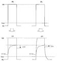
- FIG. It is a schematic diagram which shows the conventional scanning pulse.
- FIG. 3 is a schematic diagram illustrating scanning pulses of the liquid crystal display device according to the first embodiment.
- 3 is a schematic diagram illustrating a configuration of a gate driver according to Embodiment 1.
- FIG. 10 is a timing chart showing the operation of the gate driver of FIG. 9.
- FIG. 3 is a schematic diagram illustrating another configuration of the gate driver according to the first embodiment. It is a table
- resistor. 12 is a timing chart illustrating an operation of the gate driver of FIG. 11. 12 is a timing chart showing another operation of the gate driver of FIG. 11. 15 is a table showing an example of register input in FIG. 14. 12 is a timing chart showing still another operation of the gate driver of FIG. 17 is a table showing an example of register input in FIG. 16. 12 is a timing chart showing still another operation of the gate driver of FIG. FIG. 19 is a table showing an example of register input in FIG. 18. FIG.
- FIG. 6 is a schematic diagram illustrating a scan pulse setting method (previous two lines) in the first embodiment.
- FIG. 3 is a schematic diagram illustrating a scan pulse setting method (rear two lines) in the first embodiment.
- FIG. 6 is a schematic diagram illustrating an example of setting each scanning pulse in the first embodiment.
- 6 is a schematic diagram illustrating an example of pixel writing polarity (H line inversion) in Embodiment 1.
- FIG. FIG. 6 is a schematic diagram illustrating an example of pixel writing polarity in Example 1 (vertical 1 dot horizontal 1 dot inversion).
- FIG. 6 is a schematic diagram illustrating an example of pixel writing polarity in Example 1 (vertical 2 dots, horizontal 1 dot inversion). 6 is a schematic diagram illustrating an example of pixel writing polarity (V-line inversion) in Embodiment 1.
- FIG. FIG. 6 is a schematic diagram illustrating a configuration of a gate driver according to a second embodiment.
- FIG. 29 is a timing chart showing an operation of the gate driver of FIG. 28.
- FIG. FIG. 10 is a schematic diagram illustrating another configuration of the gate driver according to the second embodiment.
- FIG. 31 is a timing chart showing an operation of the gate driver of FIG. 30.
- FIG. FIG. 31 is a timing chart showing still another operation of the gate driver of FIG. 30.
- FIG. 31 is a timing chart showing still another operation of the gate driver of FIG. 30.
- FIG. 6 is a schematic diagram illustrating a configuration of a liquid crystal display device of Example 3.
- FIG. 6 is a schematic diagram illustrating a pixel configuration and a scan pulse input configuration of a liquid crystal display device of Example 3.
- FIG. 9 is a schematic diagram illustrating a scan pulse setting method (previous two lines) in Example 3.
- FIG. 10 is a schematic diagram illustrating a scan pulse setting method (rear two lines) in the third embodiment.
- FIG. 10 is a schematic diagram illustrating an example of pixel writing polarity (H line inversion) in Example 3.
- FIG. 6 is a schematic diagram illustrating an example of pixel writing polarity in Example 3 (vertical 1 dot horizontal 1 dot inversion).
- FIG. 10 is a schematic diagram illustrating an example of pixel writing polarity in Example 3 (vertical 2 dots, horizontal 1 dot inversion).
- FIG. 10 is a schematic diagram illustrating an example of pixel writing polarity in Example 3 (V-line inversion). It is a schematic diagram which shows one structural example of this liquid crystal display device.
- the term “column direction (the direction perpendicular to the column direction is the row direction)” is used for convenience of description.
- the “column direction” may be the vertical direction or the horizontal direction.
- FIG. 1 is a schematic diagram illustrating the configuration of the liquid crystal display device according to the first embodiment.
- the liquid crystal display device 1 includes a liquid crystal panel 2, a driver 5 in which a scanning signal line driving circuit and a data signal line driving circuit are integrated on one chip, and a display control circuit 4.
- the liquid crystal panel 2 is driven by a driver 5, and the driver 5 is controlled by a display control circuit 4.
- the liquid crystal panel 2 includes an active matrix substrate, a counter substrate (for example, a color filter substrate), and a liquid crystal layer disposed between the two substrates, and a plurality of subpixels are provided in a matrix on the display unit.
- the non-display portion is provided with four wirings Ha (first wiring), Hb (third wiring), Hc (second wiring), and Hd (fourth wiring).
- Each sub-pixel includes a pixel electrode formed on the active matrix substrate, a counter electrode formed on the counter substrate, and a liquid crystal layer between the pixel electrode and the corresponding electrode, and has a plurality of primary colors (for example, red, green, and blue). Display one.
- the pixel electrode of each subpixel is connected to a data signal line through a transistor, and this transistor is connected to a scanning signal line. Note that the data signal lines extend in the column direction, and the scanning signal lines extend in the row direction.
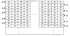
- One pixel is composed of three sub-pixels arranged in the column direction (scanning direction) that display different primary colors (triple scan method).
- the pixel P in FIG. 1 includes R (red) sub-pixels, G (green) sub-pixels, and B (blue) sub-pixels arranged in the column direction.
- the G sub-pixel is driven by the data signal line D and the scanning signal line Gb (third scanning signal line)
- the B sub-pixel is Driven by the data signal line D and the scanning signal line Gc (second scanning signal line).
- the sub pixel (R) adjacent to the downstream side of the B sub pixel in the scanning direction is driven by the data signal line D and the scanning signal line Gd (fourth scanning signal line).
- the scanning signal lines Ga to Gd are arranged in this order along the scanning direction.
- a plurality of sub-pixels arranged in the row direction are driven by the same scanning signal line and display the same primary color.
- a plurality of subpixels included in the same row as the R subpixel of the pixel P are driven by the scanning signal line Ga to display R.
- a plurality of sub-pixels included in the same row as the G sub-pixel of the pixel P are driven by the scanning signal line Gb to display R.
- a plurality of sub-pixels included in the same row as the B sub-pixel of the pixel P are driven by the scanning signal line Gc to display B.
- the scanning signal line Ga is connected to the driver 5 via the wiring Ha
- the scanning signal line Gb is connected to the driver 5 via the wiring Hb
- the scanning signal line Gc is connected to the driver 5 via the wiring Hc.
- the scanning signal line Gd is connected to the driver 5 via the wiring Hd
- the scanning pulse output from the driver 5 is supplied to the scanning signal lines Ga to Gd via the wirings Ha to Hd.
- the display unit of the liquid crystal panel 2 has a rectangular shape surrounded by the first and second short sides E1 and E2 and the four sides of the first and second long sides, and the wirings Ha and Hc have the first short side E1.
- the wirings Hb and Hd pass through the outside of the second short side E2.
- FIG. 2 is a cross-sectional view showing the structure of the active matrix substrate in region X (region surrounded by oblique lines) in FIG.
- a wiring Ha is formed on a transparent substrate (glass substrate) 30 (on the gate layer GL)
- a gate insulating film 21 is formed so as to cover the wiring Ha
- a source insulating film 21 is formed on the gate insulating film 21 (source A wiring Hc is formed on the layer SL
- an inorganic interlayer insulating film 25 is formed so as to cover the wiring Hc
- a thicker organic interlayer insulating film 26 is formed on the inorganic interlayer insulating film 25.
- the wiring Hb is formed in the same layer (gate layer GL) as the wiring Ha
- the wiring Hd is formed in the same layer (source layer SL) as the wiring Hc.
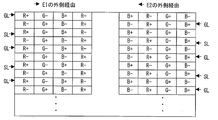
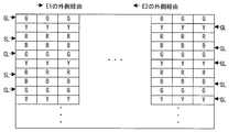
- FIG. 3 shows a corresponding primary color, a formation layer (GL or SL) of a connected wiring, and a via area (outside of the first short side E1 or outside of the second short side E2) for each subpixel row. Let me show you.
- the non-display portion can be reduced (narrow frame).
- FIG. 4 is a plan view of a portion corresponding to the pixel P (see FIG. 1) of the active matrix substrate.
- the pixel electrode 17a of the R sub-pixel, the pixel electrode 17b of the G sub-pixel, and the pixel electrode 17c of the B sub-pixel are arranged in the scanning direction along the data signal line D.
- a scanning signal line Ga is disposed between the electrode 17a and the pixel electrode 17b, and a scanning signal line Gb is disposed between the pixel electrode 17b and the pixel electrode 17c.
- a part of the scanning signal line Ga is a gate electrode of the transistor 12, the source electrode 7 of the transistor 12 is connected to the data signal line D, the drain electrode 8 of the transistor 12 is connected to the drain extraction electrode 27, and the drain extraction The electrode 27 is connected to the pixel electrode 17 a through the contact hole 11. Further, the capacitor electrode 127 formed in the same layer as the data signal line D is connected to the pixel electrode 17a through the contact hole 111, and the capacitor electrode 127 and the storage capacitor wiring 18 overlap with each other through the gate insulating film.
- . 5 is a cross-sectional view taken along the line Y-Y 'of FIG. As shown in FIG.
- the scanning signal line Ga and the storage capacitor line 18 are formed on the transparent substrate (glass substrate) 30, and the gate insulating film 21 is formed so as to cover the scanning signal line Ga and the storage capacitor line 18.
- a data signal line D and a drain lead electrode 27 are formed on the gate insulating film 21, an inorganic interlayer insulating film 25 is formed so as to cover the data signal line D and the drain lead electrode 27, and on the inorganic interlayer insulating film 25,
- a thicker organic interlayer insulating film 26 is formed, and a pixel electrode 17 a is formed on the organic interlayer insulating film 26.
- the inorganic interlayer insulating film 25 and the organic interlayer insulating film 26 are removed, so that the pixel electrode 17a and the drain lead electrode 27 are in contact with each other.
- FIG. 6A is an equivalent circuit diagram of the R subpixel and the B subpixel of the pixel P (see FIG. 1).
- a liquid crystal capacitor CLC is formed between the pixel electrode 17a and the counter electrode COM
- a storage (storage) capacitor CCS is formed between the pixel electrode 17a and the storage capacitor wiring 18, and the pixel electrode 17a
- a parasitic capacitance Cgd is formed between the scanning signal line Ga connected to the wiring Ha.
- the parasitic capacitance Cgd is generated, for example, in an overlapping portion between the scanning signal line Ga and the drain electrode 8 and the drain extraction electrode 27 in FIGS.
- FIG. 6B is an equivalent circuit diagram of the B subpixel of the pixel P (see FIG. 1).
- a liquid crystal capacitor CLC ′ is formed between the pixel electrode 17c and the counter electrode COM, and a storage (storage) capacitor CCS ′ is formed between the pixel electrode 17c and the storage capacitor wiring 18, and the pixel electrode A parasitic capacitance Cgd ′ is formed between 17c and the scanning signal line Gc connected to the wiring Hc.
- the potential V (17a) of the pixel electrode 17a is drawn due to the parasitic capacitance Cgd when the transistor 12 is OFF (at the fall of the scanning pulse GPa supplied to the scanning signal line Ga).
- the potential V (17c) of 17c is drawn due to the parasitic capacitance Cgd 'when the transistor 12' is OFF (at the fall of the scanning pulse GPc supplied to the scanning signal line Gc).
- the pull-in voltage ⁇ va generated in the pixel electrode 17a is generated in the pixel electrode 17c. Is considerably larger than the actual voltage ⁇ vc, it has been found to be a horizontal-striped display unevenness. This is because the time constant of the wiring Ha (connected to the scanning signal line Ga) formed in the gate layer is the time constant of the wiring Hc (connected to the scanning signal line Gc) formed in the metal layer (parasitic capacitance and parasitic resistance). 7 (b), the scanning pulse gpa supplied to the scanning signal line Ga rises more steeply than the scanning pulse gpc supplied to the scanning signal line Gc. Because it goes down.
- the end of the scanning pulse GPa output from the driver 5 to the wiring Ha portion from the active level to the inactive level
- An inclined portion K is provided at each end (portion from the active level to the inactive level) of the scanning pulse GPc to be performed.
- the difference between the pull-in voltage ⁇ va generated in the pixel electrode 17a and the pull-in voltage ⁇ vc generated in the pixel electrode 17c can be reduced (see FIG. 8), and the above-described horizontal stripe-shaped display unevenness can be suppressed. it can.
- the end of the scanning pulse GPb output from the driver 5 to the wiring Hb and the end of the scanning pulse GPd output from the driver 5 to the wiring Hd are each provided with an inclined portion having the same shape as the end of the scanning pulses GPa and GPc. .
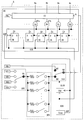
- FIG. 9 shows a configuration example of the driver 5 that generates the scanning pulses GPa to GPd including the inclined portion at the end in this way.
- 9 includes a timing controller Tcon, an inverter INV, a P-channel transistor Tp, an N-channel transistor Tn, a gate circuit GC including a shift register (not shown), a level shifter LS, and a potential of VGH.
- the plurality of output ends of the gate circuit GC are connected to the corresponding wirings Ha to Hd, the output end of the level shifter LS is connected to the input end of the inverter INV, and the output end of the inverter INV is the gate terminal of the transistor Tp and the transistor Tn Connected to the gate terminal, the node Nx is connected to the node Ny via the transistor Tp, and the node Nx is connected to one end of the resistor Rx provided outside the driver 5 and provided outside the driver 5. The other end of the resistor Rx is grounded via the transistor Tn, and the node Ny is connected to the output end of a DC-DC converter (not shown) and provided outside the driver 5. It is grounded via the capacitor Cy.
- the potential Vi of the node Nx is supplied to the gate circuit GC, the potential VGH is supplied to the node Ny, the potential VGL is supplied to the gate circuit GC, and the gate clock GCK and the gate start pulse GSP are supplied from the timing controller Tcon to the gate circuit GC. And the slope clock SLCK is supplied from the timing controller Tcon to the level shifter LS.
- FIG. 10 is a timing chart showing the operation of the driver 5 of FIG.
- Each of the gate clock GCK and the slope clock SLCK is composed of the first to fourth periods (the first to third periods are “H” and the fourth period is “L”), and the third period ( H)) and the fourth period (L) of the slope clock SLCK.
- the slope clock SLCK is in the first to third periods (H)
- the transistor Tp in FIG. 9 is turned on
- the transistor Tn is turned off
- the potential Vi VGH supplied to the gate circuit GC
- the capacitor Cx is also charged to VGH. Is done.
- the slope clock SLCK is in the fourth period (L)
- Each stage of the gate circuit GC corresponds to one scanning signal line (wiring), and takes in the gate clock GCK in accordance with the inactivation (falling) of the output (or gate start pulse GSP) of the previous stage, With the activation (rise) of the output of the subsequent stage, the capture of the gate clock GCK is terminated, and Vi is output to the corresponding wiring only during the period when the captured gate clock GCK is “H”, and the other (captured GCK VGL is output to the corresponding wiring during a period when “L” is “L” and when GCK is not captured. As a result, scan pulses GPa to GPd as shown in FIG. 10 are output to the wirings Ha to Hd.
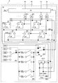
- Another configuration example of the driver 5 is shown in FIG.
- the driver 5 in FIG. 11 includes a timing controller Tcon, a slope destination potential setting circuit SVC, a slope amount setting circuit SRC, a slope clock generation circuit SGC, a slope switch circuit SSC, a gate circuit GC including a shift register, A VGL power source, a potential VSS power source, a potential AVDD power source, a potential VDD power source, a potential VCl power source, and a potential VGH power source (VGL ⁇ VSS ⁇ VDD ⁇ VCl ⁇ AVDD ⁇ VGH).
- VGH is a gate ON voltage
- AVDD is a source analog voltage
- VCI is a driver input voltage (for example, 3.3 V)
- VDD is a logic voltage inside the chip
- VSS is GND
- VGL is a gate OFF voltage.
- a plurality of output ends of the gate circuit GC are connected to the corresponding wirings Ha to Hd, a gate clock GCK and a gate start pulse GSP are supplied from the timing controller Tcon to the gate circuit GC, and a gate is supplied from the timing controller Tcon to the slope clock generation circuit SGC.
- the clock GCK is supplied, and the potential VGL is supplied to the gate circuit GC.
- the slope clock generation circuit SGC sets the slope width according to the input data D0 to D5 to the register RE1 (see FIG. 12A), and further generates the slope clock SLCK using the gate clock GCK.
- the slope clock SLCK is supplied to the slope switch circuit SSC.
- the slope destination potential setting circuit SVC has a node N1, and the node N1 is used as a power source of potential VSS, potential AVDD, potential VDD, or potential VCl according to input data D0 to D1 to the register RE2. Connect (see FIG. 12B).
- the slope switch circuit SSC has nodes N2 to N4, and this node N2 is connected to one of the nodes N3 and N4 according to the slope clock SLCK.
- the node N3 is connected to the power supply of the potential VGH, and the node N4 is connected to the node N1 via the slope amount setting circuit SRC.
- the slope amount setting circuit SRC is a variable resistor, and is set to a resistance value corresponding to the input data D0 to D3 to the register RE3.
- the number of transistors corresponding to the input data is turned on, and resistors equal to the number of turned on transistors are connected in parallel. That is, as the number of ON transistors increases, the resistance decreases and the slope becomes steeper (see FIG. 12C). Then, the potential Vi of the node N2 is supplied to the gate circuit GC.
- FIG. 13 is a timing chart showing the operation of the driver 5 of FIG.
- Each of the gate clock GCK and the slope clock SLCK is composed of the first to fourth periods (the first to third periods are “H” and the fourth period is “L”), and the third period ( H)) and the fourth period (L) of the slope clock SLCK.
- the slope clock SLCK is in the first to third periods (H)
- the slope clock SLCK When the slope clock SLCK is in the fourth period (L), the node N2 and the node N4 of the slope switch circuit SSC are connected, and the potential Vi supplied to the gate circuit GC is changed from VGH to the slope destination potential setting circuit SVC.
- the voltage gradually decreases to the set potential (any one of VSS, AVDD, VDD, VCl, and potential VGH).
- the inclination (potential decrease amount per unit time) is set by the slope amount setting circuit SRC, and becomes steep (inclination increases) as the resistance value of the slope amount setting circuit SRC decreases.
- Each stage of the gate circuit GC corresponds to one scanning signal line (wiring), and takes in the gate clock GCK in accordance with the inactivation (falling) of the output (or gate start pulse GSP) of the previous stage, With the activation (rise) of the output of the subsequent stage, the capture of the gate clock GCK is terminated, and Vi is output to the corresponding wiring only during the period when the captured gate clock GCK is “H”, and the other (captured GCK VGL is output to the corresponding wiring during a period when “L” is “L” and when GCK is not captured. As a result, scan pulses GPa to GPd as shown in FIG. 13 are output to the wirings Ha to Hd.
- the scanning pulses GPa to GPd output to the wirings Ha to Hd have the same waveform, but the present invention is not limited to this.
- the input data D0 to D5 to the register RE1 of the slope clock generation circuit SGC (see FIG. 11) is periodically exchanged to output to the wirings Ha and Hb (small time constant).
- the slopes of the scanning pulses GPa and GPb are made the same as the slopes of the slopes of the scanning pulses GPa and GPb and the slopes of the slopes of the scanning pulses GPc and GPd output to the wirings Hc and Hd (large time constant). Can be made larger than the width of the inclined portion of the scan pulses GPc and GPd.
- the input data D0 to D3 to the register RE3 of the slope amount setting circuit SRC are periodically switched to output to the wirings Ha and Hb (small time constant).
- the slopes of the scan pulses GPa and GPb are made the same with the widths of the slopes of the scan pulses GPa and GPb and the widths of the slopes of the scan pulses GPc and GPd output to the wires Hc and Hd (large time constant) Can be made larger than the inclination of the inclined portion of the scanning pulses GPc and GPd.
- the input data D0 to D5 to the register RE1 of the slope clock generation circuit SGC are periodically switched to output to the wirings Ha and Hb (small time constant).
- the scan pulse GPa / GPb is provided with an inclined portion, and the scan pulse GPc / GPd output to the wirings Hc / Hd (large time constant) is not provided with an inclined portion (the end is substantially the time axis with respect to the time axis). Vertical).
- the scanning pulse GPa is supplied to the scanning signal line Ga corresponding to the R (red) sub-pixel row via the GL wiring (Ha) on the left of the display unit, and the scanning pulse GPb Is supplied to the scanning signal line Gb corresponding to the G (green) sub-pixel row via the GL wiring (Hb) on the right side of the display unit, and the scanning pulse GPc is transmitted to the B (
- the scanning signal line Gc corresponding to the sub-pixel row of blue) is supplied to the scanning signal line Gc, and the scanning pulse GPd is supplied to the scanning signal line Gd corresponding to the sub-pixel row of R (red) via the SL wiring (Hd) on the right of the display unit.
- the shape of the end of the scanning pulses GPa to GPd can be set as follows, for example.
- the input data to the register RE3 of the slope amount setting circuit SRC (see FIG. 11) is D1, and the subpixel row (k is a natural number 4k ⁇ 3) connected to the left GL wiring.
- the predetermined gradation (for example, halftone) is displayed on the second sub-pixel row), and the luminance is measured with the other sub-pixel row being displayed in black, and the result is set as a specified value.
- the input data to the register RE3 is set to D1, and the predetermined gradation is displayed on the sub-pixel row (4k-2nd sub-pixel row) connected to the GL wiring on the right side of the display section, and another sub-pixel row is displayed.
- the luminance is measured with black display, and if it is different from the specified value, the input data to the register RE3 is changed to D2, and the measured value is adjusted to the specified value. Further, as shown in FIG. 22, the input data to the register RE3 is set to D1, and the predetermined gradation is displayed on the sub-pixel row (4k-1th sub-pixel row) connected to the SL wiring on the left side of the display unit. At the same time, the luminance is measured with the other sub-pixel row displayed in black, and if it is different from the specified value, the input data to the register RE3 is changed to D3, and the measured value is adjusted to the specified value.
- the input data to the register RE3 is set to D1, and the predetermined gradation is displayed on the sub-pixel row (4kth sub-pixel row) connected to the SL wiring on the right side of the display portion, and the other sub-pixel rows are black.
- the brightness is measured as a display, and if it is different from the specified value, the input data to the register RE3 is changed to D4, and the measured value is adjusted to the specified value.
- measurement and register settings are performed for the (4k-3) th, (4k-2) th, (4k-1), and 4kth subpixel rows, but the present invention is not limited to this.
- measurement and register setting are performed only for the (4k-3) th and (4k-1) th subpixel rows, and (4k-2)
- the register setting of the first subpixel row is the same as the (4k-3) th subpixel row
- the register setting of the (4k-1) th subpixel row is the same as the (4k-1) th subpixel row. You can also.
- FIG. 24 to 27 are schematic diagrams illustrating examples of the polarity of the signal potential written to each sub-pixel.
- FIG. 24 shows a three-gate line inversion method, in which the signal potential supplied to each data signal line is inverted every 3H (horizontal scanning period) and applied to one of the two data signal lines adjacent to the same horizontal scanning period. The polarity of the signal potential supplied is the same as the polarity of the signal potential supplied to the other.
- FIG. 25 shows a vertical one-dot horizontal one-dot inversion method, in which the signal potential supplied to each data signal line is inverted every 1H (horizontal scanning period), and two data signal lines adjacent to the same horizontal scanning period.
- FIG. 26 shows a vertical 2 dot horizontal 1 dot inversion method, in which the signal potential supplied to each data signal line is inverted every 2H (horizontal scanning period), and two data signal lines adjacent to the same horizontal scanning period. The polarity of the signal potential supplied to one of the two is opposite to the polarity of the signal potential supplied to the other.
- FIG. 27 shows a source line inversion method in which the signal potential supplied to each data signal line is inverted every 1V (vertical scanning period) and supplied to one of two data signal lines adjacent to the same horizontal scanning period. The polarity of the signal potential applied is opposite to the polarity of the signal potential supplied to the other.
- Example 2 In the configuration in which three sub-pixels constituting one pixel are arranged in the column direction (scanning direction), the number of scanning signal lines to be scanned increases (three times that in the configuration in which three sub-pixels are arranged in the row direction). Insufficient charge of the pixel electrode is likely to occur (especially when it is assumed to be used at a low temperature such as an in-vehicle liquid crystal display device). In order to solve this problem, precharge is effective.
- the driver 5 can be configured as shown in FIG. 28 and operated as shown in FIG.
- the gate circuit GC of FIG. 11 is provided with a shift register using a D flip-flop and an AND circuit corresponding to each stage of the shift register.
- the gate clock GCK from the timing controller Tcon is input to the CK terminal of each D flip-flop, and the D terminal of each D flip-flop is connected to the Q (output) terminal in the previous stage, and the Q (output terminal) is in the subsequent stage. Connected to the D terminal.
- the AND of the output of each D flip-flop and the gate clock GCK is input to the output circuit OC, and the potential Vi and the potential VGL of the node N2 are supplied to the output circuit OC.
- the Q terminal of the D flip-flop Fa corresponding to the wiring Ha is connected to the D terminal of the D flip-flop Fb corresponding to the wiring Hb
- the Q terminal of the D flip-flop Fb corresponds to the D flip-flop Fc corresponding to the wiring Hc.
- the output of the D flip-flop Fa and the gate clock GCK are input to the AND circuit Aa
- the output of the D flip-flop Fb and the gate clock GCK are input to the AND circuit Ab.
- the output APa of the circuit Aa and the output APb of the AND circuit Ab are input to the output circuit OC.
- the gate start pulse GSP is input to the D terminal of the first stage D flip-flop.
- each of the gate clock GCK and the slope clock SLCK is composed of the first to fourth periods (the first to third periods are “H” and the fourth period is “L”).
- the third period (H)) and the fourth period (L) of the slope clock SLCK overlap.
- the gate start pulse GSP becomes active twice, the first time is synchronized with a certain cycle of the gate clock GCK (becomes active in the first to fourth periods), and the second is the next of this GCK cycle. Synchronized with the next cycle.
- the slope clock SLCK When the slope clock SLCK is in the fourth period (L), the node N2 and the node N4 of the slope switch circuit SSC are connected, and the potential Vi supplied to the output circuit OC is set from VGH by the slope destination potential setting circuit SVC. Gradually decrease to the applied potential (VSS, AVDD, VDD, and VCl).
- the inclination (potential decrease amount per unit time) is set by the slope amount setting circuit SRC, and becomes steep (inclination increases) as the resistance value of the slope amount setting circuit SRC decreases.
- Each D flip-flop transfers the input of the D terminal to the Q terminal when the gate clock signal GCK rises from “L” to “H”. That is, the output Q of the own stage is activated (rises) at the same time as the output Q of the previous stage is deactivated (falls), and is inactive at the same time as the output Q of the next stage is activated (rises). (Fall down). Then, the output of the AND circuit to which the output Q and GCK of its own stage are input is input to the output circuit OC, and the output circuit OC applies Vi to the corresponding wiring only during the period when the output of the AND circuit is “H”. VGL is output to the corresponding wiring in other cases (period in which the output of the AND circuit of the own stage is “L”).
- scanning pulses GPa to GPd that are activated twice at intervals are output to the wirings Ha to Hd, and the scanning signal lines Ga to Gd are signals corresponding to two lines before. It is precharged by the potential (the same polarity as the signal potential of the main charge). Thereby, the problem of insufficient charging of the pixel electrode can be solved.
- the driver 5 can be configured as shown in FIG. 30 and operated as shown in FIG.
- the gate circuit GC of FIG. 11 is provided with a two-stage shift register using D flip-flops, and an AND circuit corresponding to each stage of the shift register, and the gate circuit GC is supplied from the timing controller Tcon.
- the gate clocks GCK1 and GCK2 and the gate start pulses GSP1 and GSP2 are supplied to the slope clock generation circuit SGC.
- the tag gate clock GCK1 is input to the CK terminal of the odd-numbered D flip-flop
- the tag gate clock GCK2 is input to the CK terminal of the even-numbered D flip-flop
- the D terminal is connected to the Q (output) terminal of the previous odd-numbered stage
- the Q (output terminal) is connected to the D terminal of the next odd-numbered stage
- the even-numbered D flip-flop is The D terminal is connected to the Q (output) terminal of the previous even numbered stage
- the Q (output terminal) is connected to the D terminal of the next even numbered stage.
- the AND of the odd-stage D flip-flop and the gate clock GCK1 is input to the output circuit OC, and the AND of the even-stage D flip-flop and the gate clock GCK2 is input to the output circuit OC.
- the potential Vi and the potential VGL of the node N2 are supplied to the OC.
- the Q terminal of the D flip-flop Fa corresponding to the wiring Ha is connected to the D terminal of the D flip-flop Fc corresponding to the wiring Hc
- the Q terminal of the D flip-flop Fb is connected to the D flip-flop Fd corresponding to the wiring Hd.
- the output of the D flip-flop Fa and the gate clock GCK1 are input to the AND circuit Aa, and the output of the D flip-flop Fb and the gate clock GCK2 are input to the AND circuit Ab.
- the output APa of the circuit Aa and the output APb of the AND circuit Ab are input to the output circuit OC.
- the gate start pulse GSP1 is input to the D terminal of the first stage D flip-flop F0, and the gate start pulse GSP2 is input to the D terminal of the second stage D flip-flop F0 '.
- each of the gate clocks GCK1 and GCK2 consists of the first to sixth periods (the first to fifth periods are “H” and the sixth period is “L”), and the sixth period ( L) and the third period (H) of GCK2 overlap.
- the slope clock SLCK consists of the first to third periods (the first and second periods are “H” and the third period is “L”).
- the sixth period (L) of GCK1 and the slope clock SLCK The first period (H) overlaps.
- the gate start pulse GSP is activated once in synchronization with a certain cycle of GCK1.
- the slope clock SLCK When the slope clock SLCK is in the third period (L), the node N2 and the node N4 of the slope switch circuit SSC are connected, and the potential Vi supplied to the output circuit OC is set from VGH by the slope destination potential setting circuit SVC.
- the voltage is gradually decreased to the set potential (any one of VSS, AVDD, VDD, VCl, and potential VGH).
- the inclination (potential decrease amount per unit time) is set by the slope amount setting circuit SRC, and becomes steep (inclination increases) as the resistance value of the slope amount setting circuit SRC decreases.
- the odd-numbered D flip-flop shifts the input of the D terminal to the Q terminal, and the even-numbered D flip-flop has the gate clock signal GCK2 of “L”.
- the input of the D terminal is transferred to the Q terminal. That is, the output Q of the own stage is activated (rises) before the output Q of the previous stage is deactivated (falls), and deactivates after the output Q of the next stage is activated (rises). (Fall down). Then, the output of the AND circuit to which the output Q of its own stage and GCK1 or GCK2 are input is input to the output circuit OC.
- the output circuit OC corresponds to Vi only during the period when the output of the AND circuit is “H”.
- VGL is output to the corresponding wiring in other cases (period in which the output of the AND circuit of the own stage is “L”).
- the scan pulses GPa to GPd in which the scan pulse of the own stage overlaps the scan pulse of the previous stage, are output to the wirings Ha to Hd, respectively, and the scan signal lines Ga to Gd correspond to the previous line. Is precharged by the signal potential (the same polarity as the signal potential of the main charge). Thereby, the problem of insufficient charging of the pixel electrode can be solved.
- the scanning pulses GPa to GPd output to the wirings Ha to Hd have the same waveform, but the present invention is not limited to this.
- the input data D0 to D5 to the register RE1 of the slope clock generation circuit SGC are periodically switched to output to the wirings Ha and Hb (small time constant).
- the slopes of the scanning pulses GPa and GPb are made the same as the slopes of the slopes of the scanning pulses GPa and GPb and the slopes of the slopes of the scanning pulses GPc and GPd output to the wirings Hc and Hd (large time constant). Can be made larger than the width of the inclined portion of the scan pulses GPc and GPd.
- the input data D0 to D3 to the register RE3 of the slope amount setting circuit SRC are periodically switched, and output to the wirings Ha and Hb (small time constant).
- the slopes of the scan pulses GPa and GPb are made the same with the widths of the slopes of the scan pulses GPa and GPb and the widths of the slopes of the scan pulses GPc and GPd output to the wires Hc and Hd (large time constant). Can be made larger than the inclination of the inclined portion of the scanning pulses GPc and GPd.
- Example 3 In the above embodiment, the three sub-pixels constituting one pixel are arranged in the column direction (scanning direction), but the present invention is not limited to this. As shown in FIG. 34, these three sub-pixels are arranged in the column direction (perpendicular to the scanning direction). As shown in FIG. 35, the scan pulse GPa is supplied to the scan signal line Ga corresponding to the first sub-pixel row via the SL wiring (Ha) on the left side of the display unit, and the scan pulse GPb is displayed on the display unit.
- the scanning signal GPc is supplied to the scanning signal line Gb corresponding to the second sub-pixel row via the right SL wiring (Hb), and the scanning pulse GPc corresponds to the third sub-pixel row via the GL wiring (Hc) on the left of the display unit.
- the scanning signal GPc may be supplied to the scanning signal line Gc, and the scanning pulse GPd may be supplied to the scanning signal line Gd corresponding to the fourth sub-pixel row via the GL wiring (Hd) on the right side of the display unit.
- the end shape of the scanning pulses GPa to GPd can be set as follows, for example.
- the input data to the register RE3 of the slope amount setting circuit SRC (see FIG. 11) is D1
- the sub-pixel row (k is a natural number 4k ⁇ 3) connected to the left GL wiring.
- the predetermined gradation (for example, halftone) is displayed on the second sub-pixel row), and the luminance is measured with the other sub-pixel row being displayed in black, and the result is set as a specified value.
- the input data to the register RE3 is set to D1, and the predetermined gradation is displayed on the sub-pixel row (4k-2nd sub-pixel row) connected to the GL wiring on the right side of the display section, and another sub-pixel row is displayed.
- the luminance is measured with black display, and if it is different from the specified value, the input data to the register RE3 is changed to D2, and the measured value is adjusted to the specified value.
- the input data to the register RE3 is set to D1, and the predetermined gradation is displayed on the sub-pixel row (4k-1th sub-pixel row) connected to the SL wiring on the left side of the display unit.
- the luminance is measured with the other sub-pixel row displayed in black, and if it is different from the specified value, the input data to the register RE3 is changed to D3, and the measured value is adjusted to the specified value.
- the input data to the register RE3 is set to D1, and the predetermined gradation is displayed on the sub-pixel row (4kth sub-pixel row) connected to the SL wiring on the right side of the display portion, and the other sub-pixel rows are black.
- the brightness is measured as a display, and if it is different from the specified value, the input data to the register RE3 is changed to D4, and the measured value is adjusted to the specified value.
- FIGS. 38 to 41 are schematic diagrams showing examples of the polarity of the signal potential written to each sub-pixel in the configuration of FIGS.
- FIG. 38 shows a one-gate line inversion method in which the signal potential supplied to each data signal line is inverted every 3H (horizontal scanning period) and is applied to one of two data signal lines adjacent to the same horizontal scanning period. The polarity of the signal potential supplied is the same as the polarity of the signal potential supplied to the other.
- FIG. 39 shows a vertical 1-dot horizontal 1-dot inversion method, in which the signal potential supplied to each data signal line is inverted every 1H (horizontal scanning period), and two data signal lines adjacent to the same horizontal scanning period.
- FIG. 40 shows a vertical 2 dot horizontal 1 dot inversion method, in which the signal potential supplied to each data signal line is inverted every 2H (horizontal scanning period), and two data signal lines adjacent to the same horizontal scanning period are displayed. The polarity of the signal potential supplied to one of the two is opposite to the polarity of the signal potential supplied to the other.
- FIG. 41 shows a source line inversion method in which the signal potential supplied to each data signal line is inverted every 1V (vertical scanning period) and supplied to one of two data signal lines adjacent to the same horizontal scanning period. The polarity of the signal potential applied is opposite to the polarity of the signal potential supplied to the other.
- the primary colors of the sub-pixels are four colors of red (R), green (G), blue (B), and Y (yellow). Is connected to the wiring passing through the outside of the first short side E1, and the scanning signal line corresponding to the yellow subpixel is formed in the gate layer GL.
- the scanning signal line corresponding to the red sub-pixel is connected to the wiring passing through the outside of the short side E2, and connected to the wiring passing through the outside of the first short side E1 to the blue sub-pixel.
- the corresponding scanning signal line may be formed in the source layer SL and connected to the wiring passing through the outside of the second short side E2. In this way, in the entire display unit, sub-pixels of the same color (particularly G or Y) are connected to wiring on the same layer and the same side (with respect to the display unit) via the scanning signal lines. It is easy to set the waveform of the scan pulse output to the wiring.
- the liquid crystal display device includes first and second scanning signal lines formed in a display portion, first and second wirings formed in a non-display portion, and a scanning signal line driving circuit. Two wirings are formed in different layers, and the scanning signal line driving circuit is connected to the first scanning signal line through the first wiring and is connected to the second scanning signal line through the second wiring, The time constant of the first wiring is smaller than the time constant of the second wiring, and the first scanning pulse output from the scanning signal line driving circuit to the first wiring is first at the end from the active level to the inactive level. An inclined portion is included.
- the first scanning pulse and the second scanning pulse when each of them is supplied to the first and second scanning signal lines via the first and second wirings, the pull-in voltage associated with the deactivation of the first scanning pulse and the deactivation of the second scanning pulse.
- the difference from the pull-in voltage associated with can be reduced.
- horizontal stripe-shaped display unevenness can be suppressed and display quality can be improved.
- the second scanning pulse output from the scanning signal line driving circuit to the second wiring may include a second inclined portion at the end from the active level to the inactive level.
- the first inclined portion and the second inclined portion may have the same shape.
- the inclination of the first inclined portion and the inclination of the second inclined portion may be the same, and the width of the first inclined portion may be larger than the width of the second inclined portion.
- the width of the first inclined portion and the width of the second inclined portion may be the same, and the inclination of the first inclined portion may be steeper than the inclination of the second inclined portion.
- the second scanning pulse output from the scanning signal line driving circuit to the second wiring has a configuration in which the end from the active level to the inactive level is substantially perpendicular to the time axis. It can also be.
- the liquid crystal display device includes a first pixel electrode, a first data signal line, and a first transistor, and the first scanning signal line, the first data signal line, and the first pixel electrode are connected to the first transistor. It can also be set as the structure which is.
- one pixel is composed of a plurality of sub-pixels arranged in the column direction with the extending direction of the first scanning signal line as the row direction, and one of the plurality of sub-pixels includes the first pixel electrode. May be included.
- each sub-pixel controlled by the first scanning signal line may be configured to have the same color.
- one of the first and second wirings may be formed in the same layer as the first data signal line, and the other may be formed in the same layer as the first and second scanning signal lines. it can.
- the present liquid crystal display device may be configured such that n is a natural number and the first scanning signal line is supplied with a precharge pulse before n horizontal scanning periods during which the first scanning pulse is supplied.
- the polarity of the signal potential output from the first data signal line may be inverted every n horizontal scanning periods.
- the liquid crystal display device includes third and fourth scanning signal lines formed in the display unit and third and fourth wirings formed in the non-display unit, and the display unit includes the first and second short lines.
- the third wiring is formed in the same layer as the first wiring
- the fourth wiring is formed in the same layer as the second wiring
- the scanning signal line is surrounded by four sides of the side and the first and second long sides.
- the drive circuit is connected to the third scanning signal line through the third wiring, and is connected to the fourth scanning signal line through the fourth wiring.
- the first and second wirings are outside the first short side.
- the third and fourth wirings can also be configured to pass through the outside of the second short side.
- the first scanning signal line, the third scanning signal line, the second scanning signal line, and the fourth scanning signal line may be arranged in the column direction in this order.
- the second to fourth scanning pulses are output from the scanning signal line driving circuit to the second to fourth wirings, respectively, and the time constant of the third wiring is smaller than the time constant of the fourth wiring.
- the third scan pulse may include a third inclined portion at the end from the active level to the inactive level.
- the present invention is not limited to the above-described embodiments, and those obtained by appropriately modifying the above-described embodiments based on common general technical knowledge and those obtained by combining them are also included in the embodiments of the present invention.
- the present invention is suitable for a liquid crystal display device that performs three-dimensional wiring in a non-display portion.
Abstract
This liquid crystal display device is provided with first and second scan signal lines formed in a display part, first and second wires formed in a non-display part, and a scan signal line driving circuit. The first and second wires are formed in different layers, the scan signal line driving circuit is connected to the first scan signal line via the first wire and connected to the second scan signal line via the second wire, the time constant of the first wire is smaller than the time constant of the second wire, and a first scan pulse outputted from the scan signal line driving circuit to the first wire includes a first inclined section at the termination thereof ranging from an active level to a non-active level. The display quality of the liquid crystal display device is improved by the abovementioned configuration.
Description
本発明は、液晶表示装置に関する。
The present invention relates to a liquid crystal display device.
表示部の複数の走査信号線と走査信号線駆動回路(ゲートドライバ)とを非表示部に形成された複数の配線を介して接続するような液晶表示装置において、非表示部の縮小化(狭額縁化)を目的として、これら複数の配線を2層に分けて配置する(立体的に配置する)構成が提案されている。
In a liquid crystal display device in which a plurality of scanning signal lines of a display portion and a scanning signal line driving circuit (gate driver) are connected via a plurality of wirings formed in the non-display portion, the non-display portion is reduced (narrowed). For the purpose of (framed), a configuration has been proposed in which these wirings are arranged in two layers (three-dimensionally arranged).
発明者は、上記構成において、2層の一方に配された第1配線の時定数(寄生容量および寄生抵抗の積)と他方に配された第2配線の時定数(寄生容量および寄生抵抗の積)との相異によって、第1配線に接続する走査信号線に供給される走査パルスと第2配線に接続する走査信号線に供給される走査パルスの波形が異なり、表示部に横縞状のムラが現れ易くなるという問題を見出した。
In the above configuration, the inventor determines the time constant of the first wiring arranged on one of the two layers (product of parasitic capacitance and parasitic resistance) and the time constant of the second wiring arranged on the other (parasitic capacitance and parasitic resistance). The waveform of the scanning pulse supplied to the scanning signal line connected to the first wiring and the scanning pulse supplied to the scanning signal line connected to the second wiring are different, and the display portion has a horizontal stripe shape. We found a problem that unevenness is likely to appear.
本発明の目的は、非表示部で立体的な配線を行う液晶表示装置の表示品位を高めることにある。
An object of the present invention is to improve the display quality of a liquid crystal display device that performs three-dimensional wiring in a non-display portion.
本液晶表示装置は、表示部に形成された第1および第2走査信号線と、非表示部に形成された第1および第2配線と、走査信号線駆動回路とを備え、第1および第2配線が異なる層に形成され、上記走査信号線駆動回路は、第1配線を介して第1走査信号線に接続されるとともに、第2配線を介して第2走査信号線に接続され、上記第1配線の時定数は、第2配線の時定数よりも小さく、上記走査信号線駆動回路から第1配線に出力される第1走査パルスは、アクティブレベルから非アクティブレベルに至る終端に第1傾斜部を含んでいることを特徴とする。
The liquid crystal display device includes first and second scanning signal lines formed in a display portion, first and second wirings formed in a non-display portion, and a scanning signal line driving circuit. Two wirings are formed in different layers, and the scanning signal line driving circuit is connected to the first scanning signal line through the first wiring and is connected to the second scanning signal line through the second wiring, The time constant of the first wiring is smaller than the time constant of the second wiring, and the first scanning pulse output from the scanning signal line driving circuit to the first wiring is first at the end from the active level to the inactive level. An inclined portion is included.
このように、時定数の小さな第1配線に出力する第1走査パルスに第1傾斜部を設けることで、第1走査パルスおよび第2走査パルス(時定数の大きな第2配線に出力される走査パルス)それぞれが第1および第2配線を介して第1および第2走査信号線に供給されたときに、第1走査パルスの非アクティブ化に伴う引き込み電圧と、第2走査パルスの非アクティブ化に伴う引き込み電圧との差を小さくすることができる。これにより、横縞状の表示ムラを抑制し、表示品位を高めることができる。
In this way, by providing the first inclined portion in the first scanning pulse output to the first wiring having a small time constant, the first scanning pulse and the second scanning pulse (scanning output to the second wiring having a large time constant). Pulse) when each of them is supplied to the first and second scanning signal lines via the first and second wirings, the pull-in voltage associated with the deactivation of the first scanning pulse and the deactivation of the second scanning pulse. Thus, the difference from the pull-in voltage associated with can be reduced. Thereby, horizontal stripe-shaped display unevenness can be suppressed and display quality can be improved.
本発明によれば、非表示部で立体的な配線を行う液晶表示装置の表示品位を高めることができる。
According to the present invention, it is possible to improve the display quality of a liquid crystal display device that performs three-dimensional wiring in a non-display portion.
本発明の実施の形態を、図1~42を用いて説明すれば、以下のとおりである。なお、液晶表示装置の説明で「列方向(この列方向に直交する方向が行方向)」との文言を用いるが、これは説明の便宜のためであって、液晶表示装置の使用状態において上記「列方向」が縦方向になっても横方向になってもよいものとする。
The embodiment of the present invention will be described with reference to FIGS. 1 to 42 as follows. In the description of the liquid crystal display device, the term “column direction (the direction perpendicular to the column direction is the row direction)” is used for convenience of description. The “column direction” may be the vertical direction or the horizontal direction.
〔実施例1〕
図1は、実施例1の液晶表示装置の構成を示す模式図である。図1に示すように、液晶表示装置1は、液晶パネル2、走査信号線駆動回路とデータ信号線駆動回路とが1チップ化されたドライバ5、および表示制御回路4を備える。液晶パネル2は、ドライバ5によって駆動され、ドライバ5は、表示制御回路4によって制御される。液晶パネル2は、アクティブマトリクス基板と、対向基板(例えば、カラーフィルタ基板)と、これら両基板間に配された液晶層とを備え、その表示部には、マトリクス状に複数のサブ画素が設けられ、その非表示部には、4本の配線Ha(第1配線)、Hb(第3配線)、Hc(第2配線)およびHd(第4配線)が設けられる。 [Example 1]
FIG. 1 is a schematic diagram illustrating the configuration of the liquid crystal display device according to the first embodiment. As shown in FIG. 1, the liquidcrystal display device 1 includes a liquid crystal panel 2, a driver 5 in which a scanning signal line driving circuit and a data signal line driving circuit are integrated on one chip, and a display control circuit 4. The liquid crystal panel 2 is driven by a driver 5, and the driver 5 is controlled by a display control circuit 4. The liquid crystal panel 2 includes an active matrix substrate, a counter substrate (for example, a color filter substrate), and a liquid crystal layer disposed between the two substrates, and a plurality of subpixels are provided in a matrix on the display unit. The non-display portion is provided with four wirings Ha (first wiring), Hb (third wiring), Hc (second wiring), and Hd (fourth wiring).
図1は、実施例1の液晶表示装置の構成を示す模式図である。図1に示すように、液晶表示装置1は、液晶パネル2、走査信号線駆動回路とデータ信号線駆動回路とが1チップ化されたドライバ5、および表示制御回路4を備える。液晶パネル2は、ドライバ5によって駆動され、ドライバ5は、表示制御回路4によって制御される。液晶パネル2は、アクティブマトリクス基板と、対向基板(例えば、カラーフィルタ基板)と、これら両基板間に配された液晶層とを備え、その表示部には、マトリクス状に複数のサブ画素が設けられ、その非表示部には、4本の配線Ha(第1配線)、Hb(第3配線)、Hc(第2配線)およびHd(第4配線)が設けられる。 [Example 1]
FIG. 1 is a schematic diagram illustrating the configuration of the liquid crystal display device according to the first embodiment. As shown in FIG. 1, the liquid
各サブ画素は、アクティブマトリクス基板に形成される画素電極、対向基板に形成される対向電極、および画素電極および対応電極間の液晶層を含み、複数の原色(例えば、赤・緑・青)の1つを表示する。各サブ画素の画素電極はトランジスタを介してデータ信号線に接続され、このトランジスタは走査信号線に接続される。なお、データ信号線は列方向に延伸し、走査信号線は行方向に延伸する。
Each sub-pixel includes a pixel electrode formed on the active matrix substrate, a counter electrode formed on the counter substrate, and a liquid crystal layer between the pixel electrode and the corresponding electrode, and has a plurality of primary colors (for example, red, green, and blue). Display one. The pixel electrode of each subpixel is connected to a data signal line through a transistor, and this transistor is connected to a scanning signal line. Note that the data signal lines extend in the column direction, and the scanning signal lines extend in the row direction.
1つの画素は、異なる原色を表示する、列方向(走査方向)に並ぶ3つのサブ画素によって構成される(トリプルスキャン方式)。例えば、図1の画素Pは、列方向に沿って並ぶ、R(赤)のサブ画素およびG(緑)のサブ画素並びにB(青)のサブ画素によって構成され、Rのサブ画素は、データ信号線Dおよび走査信号線Ga(第1走査信号線)によって駆動され、Gのサブ画素は、データ信号線Dおよび走査信号線Gb(第3走査信号線)によって駆動され、Bのサブ画素は、データ信号線Dおよび走査信号線Gc(第2走査信号線)によって駆動される。また、Bのサブ画素の走査方向下流側に隣接するサブ画素(R)は、データ信号線Dおよび走査信号線Gd(第4走査信号線)によって駆動される。なお、走査信号線Ga~Gdは、走査方向に沿ってこの順に並べられている。
One pixel is composed of three sub-pixels arranged in the column direction (scanning direction) that display different primary colors (triple scan method). For example, the pixel P in FIG. 1 includes R (red) sub-pixels, G (green) sub-pixels, and B (blue) sub-pixels arranged in the column direction. Driven by the signal line D and the scanning signal line Ga (first scanning signal line), the G sub-pixel is driven by the data signal line D and the scanning signal line Gb (third scanning signal line), and the B sub-pixel is Driven by the data signal line D and the scanning signal line Gc (second scanning signal line). Further, the sub pixel (R) adjacent to the downstream side of the B sub pixel in the scanning direction is driven by the data signal line D and the scanning signal line Gd (fourth scanning signal line). The scanning signal lines Ga to Gd are arranged in this order along the scanning direction.
行方向に並ぶ複数のサブ画素(同一行に含まれる複数のサブ画素)は同一の走査信号線によって駆動され、同一の原色を表示する。例えば、画素PのRのサブ画素と同一行に含まれる複数のサブ画素は走査信号線Gaによって駆動され、Rを表示する。また、画素PのGのサブ画素と同一行に含まれる複数のサブ画素は走査信号線Gbによって駆動され、Rを表示する。また、画素PのBのサブ画素と同一行に含まれる複数のサブ画素は走査信号線Gcによって駆動され、Bを表示する。
A plurality of sub-pixels arranged in the row direction (a plurality of sub-pixels included in the same row) are driven by the same scanning signal line and display the same primary color. For example, a plurality of subpixels included in the same row as the R subpixel of the pixel P are driven by the scanning signal line Ga to display R. A plurality of sub-pixels included in the same row as the G sub-pixel of the pixel P are driven by the scanning signal line Gb to display R. A plurality of sub-pixels included in the same row as the B sub-pixel of the pixel P are driven by the scanning signal line Gc to display B.
そして、走査信号線Gaは、配線Haを介してドライバ5に接続され、走査信号線Gbは、配線Hbを介してドライバ5に接続され、走査信号線Gcは、配線Hcを介してドライバ5に接続され、走査信号線Gdは、配線Hdを介してドライバ5に接続され、ドライバ5から出力された走査パルスは、配線Ha~Hdを介して走査信号線Ga~Gdに供給される。なお、液晶パネル2の表示部は、第1および第2短辺E1・E2並びに第1および第2長辺の4辺で囲まれた長方形形状であり、配線Ha・Hcは第1短辺E1の外側を経由し、配線Hb・Hdは第2短辺E2の外側を経由している。
The scanning signal line Ga is connected to the driver 5 via the wiring Ha, the scanning signal line Gb is connected to the driver 5 via the wiring Hb, and the scanning signal line Gc is connected to the driver 5 via the wiring Hc. The scanning signal line Gd is connected to the driver 5 via the wiring Hd, and the scanning pulse output from the driver 5 is supplied to the scanning signal lines Ga to Gd via the wirings Ha to Hd. The display unit of the liquid crystal panel 2 has a rectangular shape surrounded by the first and second short sides E1 and E2 and the four sides of the first and second long sides, and the wirings Ha and Hc have the first short side E1. The wirings Hb and Hd pass through the outside of the second short side E2.
図2は、図1の領域X(斜線で囲んだ領域)のアクティブマトリクス基板の構造を示す断面図である。図2に示すように、透明基板(ガラス基板)30上に(ゲート層GLに)配線Haが形成され、配線Haを覆うようにゲート絶縁膜21が形成され、ゲート絶縁膜21上に(ソース層SLに)配線Hcが形成され、配線Hcを覆うように無機層間絶縁膜25が形成され、無機層間絶縁膜25上に、これよりも厚い有機層間絶縁膜26が形成されている。なお、図示しないが、配線Hbは配線Haと同層(ゲート層GL)に形成され、配線Hdは配線Hcと同層(ソース層SL)に形成されている。図3に、各サブ画素行についての、対応する原色、接続される配線の形成層(GLまたはSL)およびこの配線の経由領域(第1短辺E1の外側または第2短辺E2の外側)を示しておく。このように、配線Ha~Hdを2層(GL・SL)に分けて形成することで、非表示部を縮小(狭額縁化)することができる。
FIG. 2 is a cross-sectional view showing the structure of the active matrix substrate in region X (region surrounded by oblique lines) in FIG. As shown in FIG. 2, a wiring Ha is formed on a transparent substrate (glass substrate) 30 (on the gate layer GL), a gate insulating film 21 is formed so as to cover the wiring Ha, and a source insulating film 21 is formed on the gate insulating film 21 (source A wiring Hc is formed on the layer SL, an inorganic interlayer insulating film 25 is formed so as to cover the wiring Hc, and a thicker organic interlayer insulating film 26 is formed on the inorganic interlayer insulating film 25. Although not shown, the wiring Hb is formed in the same layer (gate layer GL) as the wiring Ha, and the wiring Hd is formed in the same layer (source layer SL) as the wiring Hc. FIG. 3 shows a corresponding primary color, a formation layer (GL or SL) of a connected wiring, and a via area (outside of the first short side E1 or outside of the second short side E2) for each subpixel row. Let me show you. Thus, by forming the wirings Ha to Hd in two layers (GL and SL), the non-display portion can be reduced (narrow frame).
図4は、アクティブマトリクス基板の画素P(図1参照)に対応する部分の平面図である。図4に示すように、Rのサブ画素の画素電極17a、Gのサブ画素の画素電極17b、およびBのサブ画素の画素電極17cが、データ信号線Dに沿って走査方向に並べられ、画素電極17aと画素電極17bとの間に走査信号線Gaが配され、画素電極17bと画素電極17cとの間に走査信号線Gbが配されている。走査信号線Gaの一部はトランジスタ12のゲート電極となっており、トランジスタ12のソース電極7はデータ信号線Dに接続され、トランジスタ12のドレイン電極8はドレイン引き出し電極27に接続され、ドレイン引き出し電極27はコンタクトホール11を介して画素電極17aに接続されている。さらに、データ信号線Dと同層に形成された容量電極127が、コンタクトホール111を介して画素電極17aに接続され、容量電極127と保持容量配線18とがゲート絶縁膜を介して重なっている。図5は図4のY-Y’断面図である。図5に示すように、透明基板(ガラス基板)30上に走査信号線Gaおよび保持容量配線18が形成され、走査信号線Gaおよび保持容量配線18を覆うようにゲート絶縁膜21が形成され、ゲート絶縁膜21上に、データ信号線Dおよびドレイン引き出し電極27が形成され、データ信号線Dおよびドレイン引き出し電極27を覆うように無機層間絶縁膜25が形成され、無機層間絶縁膜25上に、これよりも厚い有機層間絶縁膜26が形成され、有機層間絶縁膜26上に画素電極17aが形成されている。なお、コンタクトホール11部分では、無機層間絶縁膜25および有機層間絶縁膜26が除去されており、これによって画素電極17aとドレイン引き出し電極27とが接触している。
FIG. 4 is a plan view of a portion corresponding to the pixel P (see FIG. 1) of the active matrix substrate. As shown in FIG. 4, the pixel electrode 17a of the R sub-pixel, the pixel electrode 17b of the G sub-pixel, and the pixel electrode 17c of the B sub-pixel are arranged in the scanning direction along the data signal line D. A scanning signal line Ga is disposed between the electrode 17a and the pixel electrode 17b, and a scanning signal line Gb is disposed between the pixel electrode 17b and the pixel electrode 17c. A part of the scanning signal line Ga is a gate electrode of the transistor 12, the source electrode 7 of the transistor 12 is connected to the data signal line D, the drain electrode 8 of the transistor 12 is connected to the drain extraction electrode 27, and the drain extraction The electrode 27 is connected to the pixel electrode 17 a through the contact hole 11. Further, the capacitor electrode 127 formed in the same layer as the data signal line D is connected to the pixel electrode 17a through the contact hole 111, and the capacitor electrode 127 and the storage capacitor wiring 18 overlap with each other through the gate insulating film. . 5 is a cross-sectional view taken along the line Y-Y 'of FIG. As shown in FIG. 5, the scanning signal line Ga and the storage capacitor line 18 are formed on the transparent substrate (glass substrate) 30, and the gate insulating film 21 is formed so as to cover the scanning signal line Ga and the storage capacitor line 18. A data signal line D and a drain lead electrode 27 are formed on the gate insulating film 21, an inorganic interlayer insulating film 25 is formed so as to cover the data signal line D and the drain lead electrode 27, and on the inorganic interlayer insulating film 25, A thicker organic interlayer insulating film 26 is formed, and a pixel electrode 17 a is formed on the organic interlayer insulating film 26. In the contact hole 11 portion, the inorganic interlayer insulating film 25 and the organic interlayer insulating film 26 are removed, so that the pixel electrode 17a and the drain lead electrode 27 are in contact with each other.
図6(a)は、画素P(図1参照)のRのサブ画素およびBのサブ画素の等価回路図である。Rのサブ画素では、画素電極17aと対向電極COMとの間に液晶容量CLCが形成され、画素電極17aと保持容量配線18との間に保持(蓄積)容量CCSが形成され、画素電極17aと配線Haに接続する走査信号線Gaとの間に寄生容量Cgdが形成される。この寄生容量Cgdは、例えば、図4・5の走査信号線Gaとドレイン電極8およびドレイン引き出し電極27との重なり部分に生じる。また、図6(b)は、画素P(図1参照)のBのサブ画素の等価回路図である。Bのサブ画素では、画素電極17cと対向電極COMとの間に液晶容量CLC’が形成され、画素電極17cと保持容量配線18との間に保持(蓄積)容量CCS’が形成され、画素電極17cと配線Hcに接続する走査信号線Gcとの間に寄生容量Cgd’が形成される。
FIG. 6A is an equivalent circuit diagram of the R subpixel and the B subpixel of the pixel P (see FIG. 1). In the R subpixel, a liquid crystal capacitor CLC is formed between the pixel electrode 17a and the counter electrode COM, a storage (storage) capacitor CCS is formed between the pixel electrode 17a and the storage capacitor wiring 18, and the pixel electrode 17a A parasitic capacitance Cgd is formed between the scanning signal line Ga connected to the wiring Ha. The parasitic capacitance Cgd is generated, for example, in an overlapping portion between the scanning signal line Ga and the drain electrode 8 and the drain extraction electrode 27 in FIGS. FIG. 6B is an equivalent circuit diagram of the B subpixel of the pixel P (see FIG. 1). In the sub-pixel B, a liquid crystal capacitor CLC ′ is formed between the pixel electrode 17c and the counter electrode COM, and a storage (storage) capacitor CCS ′ is formed between the pixel electrode 17c and the storage capacitor wiring 18, and the pixel electrode A parasitic capacitance Cgd ′ is formed between 17c and the scanning signal line Gc connected to the wiring Hc.
ここで、画素電極17aの電位V(17a)は、トランジスタ12のOFF時(走査信号線Gaに供給される走査パルスGPaの立ち下り時)に、寄生容量Cgdに起因して引き込まれ、画素電極17cの電位V(17c)は、トランジスタ12’のOFF時(走査信号線Gcに供給される走査パルスGPcの立ち下り時)に、寄生容量Cgd’に起因して引き込まれるが、ドライバ5から配線Haに出力する走査パルスGPaおよびドライバ5から配線Hcに出力する走査パルスGPcを図7(a)のように同一の矩形(非アクティブ電位VGL<対向電極の電位VCOM<アクティブ電位VGH)とすると、寄生容量Cgd=寄生容量Cgd’であっても、画素電極17aに生じる引き込み電圧Δvaが、画素電極17cに生じる引き込み電圧Δvcよりもかなり大きくなって、横縞状の表示ムラとなることが見出された。これは、ゲート層に形成される配線Ha(走査信号線Gaに接続)の時定数が、メタル層に形成される配線Hc(走査信号線Gcに接続)の時定数(寄生容量および寄生抵抗の積)よりも小さいことに起因して、図7(b)に示すように、走査信号線Gaに供給される走査パルスgpaが、走査信号線Gcに供給される走査パルスgpcよりも急峻に立ち下がるからである。
Here, the potential V (17a) of the pixel electrode 17a is drawn due to the parasitic capacitance Cgd when the transistor 12 is OFF (at the fall of the scanning pulse GPa supplied to the scanning signal line Ga). The potential V (17c) of 17c is drawn due to the parasitic capacitance Cgd 'when the transistor 12' is OFF (at the fall of the scanning pulse GPc supplied to the scanning signal line Gc). When the scanning pulse GPa output to Ha and the scanning pulse GPc output from the driver 5 to the wiring Hc have the same rectangular shape (inactive potential VGL <potential of the counter electrode VCOM <active potential VGH) as shown in FIG. Even if the parasitic capacitance Cgd = parasitic capacitance Cgd ′, the pull-in voltage Δva generated in the pixel electrode 17a is generated in the pixel electrode 17c. Is considerably larger than the actual voltage Δvc, it has been found to be a horizontal-striped display unevenness. This is because the time constant of the wiring Ha (connected to the scanning signal line Ga) formed in the gate layer is the time constant of the wiring Hc (connected to the scanning signal line Gc) formed in the metal layer (parasitic capacitance and parasitic resistance). 7 (b), the scanning pulse gpa supplied to the scanning signal line Ga rises more steeply than the scanning pulse gpc supplied to the scanning signal line Gc. Because it goes down.
そこで、実施例1の液晶表示装置では、図8に示すように、ドライバ5から配線Haに出力する走査パルスGPaの終端(アクティブレベルから非アクティブレベルに至る部分)およびドライバ5から配線Hcに出力する走査パルスGPcの終端(アクティブレベルから非アクティブレベルに至る部分)それぞれに傾斜部Kを設けている。
Therefore, in the liquid crystal display device according to the first embodiment, as shown in FIG. 8, the end of the scanning pulse GPa output from the driver 5 to the wiring Ha (portion from the active level to the inactive level) and the output from the driver 5 to the wiring Hc. An inclined portion K is provided at each end (portion from the active level to the inactive level) of the scanning pulse GPc to be performed.
これにより、画素電極17aに生じる引き込み電圧Δvaと、画素電極17cに生じる引き込み電圧Δvcとを差を小さくすることができ(図8参照)、上記のような横縞状の表示ムラを抑制することができる。なお、ドライバ5から配線Hbに出力する走査パルスGPbの終端およびドライバ5から配線Hdに出力する走査パルスGPdの終端それぞれについても、走査パルスGPa・GPcの終端と同一形状の傾斜部を設けている。
As a result, the difference between the pull-in voltage Δva generated in the pixel electrode 17a and the pull-in voltage Δvc generated in the pixel electrode 17c can be reduced (see FIG. 8), and the above-described horizontal stripe-shaped display unevenness can be suppressed. it can. Note that the end of the scanning pulse GPb output from the driver 5 to the wiring Hb and the end of the scanning pulse GPd output from the driver 5 to the wiring Hd are each provided with an inclined portion having the same shape as the end of the scanning pulses GPa and GPc. .
このように終端に傾斜部を含む走査パルスGPa~GPdを生成するドライバ5の構成例を図9に示す。図9のドライバ5は、タイミングコントローラTconと、インバータINVと、PチャネルトランジスタTpと、NチャネルトランジスタTnと、シフトレジスタ(図示せず)を含むゲート回路GCと、レベルシフタLSと、電位がVGHの電源と、電位がVGLの電源とを備える。ゲート回路GCの複数の出力端が対応する配線Ha~Hdに接続され、レベルシフタLSの出力端はインバータINVの入力端に接続され、インバータINVの出力端は、トランジスタTpのゲート端子およびトランジスタTnのゲート端子に接続され、ノードNxがトランジスタTpを介してノードNyに接続され、ノードNxは、ドライバ5の外部に設けられた抵抗Rxの一端に接続されるとともに、ドライバ5の外部に設けられた容量Cxを介して接地され、抵抗Rxの他端は、トランジスタTnを介して接地され、ノードNyは、図示しないDC-DCコンバータの出力端に接続されるともに、ドライバ5の外部に設けられた容量Cyを介して接地されている。そして、ノードNxの電位Viがゲート回路GCに供給され、ノードNyに電位VGHが供給され、ゲート回路GCに電位VGLが供給され、タイミングコントローラTconからゲート回路GCにゲートクロックGCKおよびゲートスタートパルスGSPが供給され、タイミングコントローラTconからレベルシフタLSにスロープクロックSLCKが供給される。
FIG. 9 shows a configuration example of the driver 5 that generates the scanning pulses GPa to GPd including the inclined portion at the end in this way. 9 includes a timing controller Tcon, an inverter INV, a P-channel transistor Tp, an N-channel transistor Tn, a gate circuit GC including a shift register (not shown), a level shifter LS, and a potential of VGH. A power source and a power source having a potential of VGL. The plurality of output ends of the gate circuit GC are connected to the corresponding wirings Ha to Hd, the output end of the level shifter LS is connected to the input end of the inverter INV, and the output end of the inverter INV is the gate terminal of the transistor Tp and the transistor Tn Connected to the gate terminal, the node Nx is connected to the node Ny via the transistor Tp, and the node Nx is connected to one end of the resistor Rx provided outside the driver 5 and provided outside the driver 5. The other end of the resistor Rx is grounded via the transistor Tn, and the node Ny is connected to the output end of a DC-DC converter (not shown) and provided outside the driver 5. It is grounded via the capacitor Cy. The potential Vi of the node Nx is supplied to the gate circuit GC, the potential VGH is supplied to the node Ny, the potential VGL is supplied to the gate circuit GC, and the gate clock GCK and the gate start pulse GSP are supplied from the timing controller Tcon to the gate circuit GC. And the slope clock SLCK is supplied from the timing controller Tcon to the level shifter LS.
図10は、図9のドライバ5の動作を示すタイミングチャートである。ゲートクロックGCKおよびスロープクロックSLCKはそれぞれ、1サイクルが第1~第4期(第1~第3期が「H」、第4期が「L」)からなり、ゲートクロックGCKの第3期(H))とスロープクロックSLCKの第4期(L)と重なっている。スロープクロックSLCKが第1~第3期(H)のときは、図9のトランジスタTpがON、トランジスタTnがOFFし、ゲート回路GCに供給される電位Vi=VGHとなり、容量CxもVGHに充電される。スロープクロックSLCKが第4期(L)のときは、図9のトランジスタTpがOFF、トランジスタTnがONし、容量Cxが抵抗RxおよびトランジスタTnを介して放電され、ゲート回路GCに供給される電位Viは、第4期をかけて、VGHからVGLよりも大きい所定電位まで漸減する(第4期中に徐々に低下する)。
FIG. 10 is a timing chart showing the operation of the driver 5 of FIG. Each of the gate clock GCK and the slope clock SLCK is composed of the first to fourth periods (the first to third periods are “H” and the fourth period is “L”), and the third period ( H)) and the fourth period (L) of the slope clock SLCK. When the slope clock SLCK is in the first to third periods (H), the transistor Tp in FIG. 9 is turned on, the transistor Tn is turned off, the potential Vi = VGH supplied to the gate circuit GC, and the capacitor Cx is also charged to VGH. Is done. When the slope clock SLCK is in the fourth period (L), the transistor Tp in FIG. 9 is turned off, the transistor Tn is turned on, the capacitor Cx is discharged through the resistor Rx and the transistor Tn, and the potential supplied to the gate circuit GC Vi gradually decreases from VGH to a predetermined potential higher than VGL over the fourth period (slowly decreases during the fourth period).
ゲート回路GCの各段は、1本の走査信号線(配線)に対応しており、前段の出力(あるいはゲートスタートパルスGSP)の非アクティブ化(立ち下がり)に伴ってゲートクロックGCKを取り込み、後段の出力のアクティブ化(立ち上がり)に伴ってゲートクロックGCKの取り込みを終了し、取り込んだゲートクロックGCKが「H」である期間のみViを、対応する配線に出力し、それ以外(取り込んだGCKが「L」である期間およびGCKを取り込まない期間)はVGLを、対応する配線に出力する。これにより、配線Ha~Hdには、図10に示すような走査パルスGPa~GPdが出力される。
ドライバ5の別の構成例を図11に示す。図11のドライバ5は、タイミングコントローラTconと、スロープ先電位設定回路SVCと、スロープ量設定回路SRCと、スロープクロック生成回路SGCと、スロープスイッチ回路SSCと、シフトレジスタを含むゲート回路GCと、電位VGLの電源、電位VSSの電源、電位AVDDの電源、電位VDDの電源、電位VClの電源、および電位がVGH電源とを備える(VGL<VSS<VDD<VCl<AVDD<VGH)。なお、VGHはゲートON電圧、AVDDはソースアナログ電圧、VCIはドライバ入力電圧(例えば、3.3V)、VDDはチップ内部のロジック電圧、VSSはGND、VGLはゲートOFF電圧である。 Each stage of the gate circuit GC corresponds to one scanning signal line (wiring), and takes in the gate clock GCK in accordance with the inactivation (falling) of the output (or gate start pulse GSP) of the previous stage, With the activation (rise) of the output of the subsequent stage, the capture of the gate clock GCK is terminated, and Vi is output to the corresponding wiring only during the period when the captured gate clock GCK is “H”, and the other (captured GCK VGL is output to the corresponding wiring during a period when “L” is “L” and when GCK is not captured. As a result, scan pulses GPa to GPd as shown in FIG. 10 are output to the wirings Ha to Hd.
Another configuration example of thedriver 5 is shown in FIG. The driver 5 in FIG. 11 includes a timing controller Tcon, a slope destination potential setting circuit SVC, a slope amount setting circuit SRC, a slope clock generation circuit SGC, a slope switch circuit SSC, a gate circuit GC including a shift register, A VGL power source, a potential VSS power source, a potential AVDD power source, a potential VDD power source, a potential VCl power source, and a potential VGH power source (VGL <VSS <VDD <VCl <AVDD <VGH). Note that VGH is a gate ON voltage, AVDD is a source analog voltage, VCI is a driver input voltage (for example, 3.3 V), VDD is a logic voltage inside the chip, VSS is GND, and VGL is a gate OFF voltage.
ドライバ5の別の構成例を図11に示す。図11のドライバ5は、タイミングコントローラTconと、スロープ先電位設定回路SVCと、スロープ量設定回路SRCと、スロープクロック生成回路SGCと、スロープスイッチ回路SSCと、シフトレジスタを含むゲート回路GCと、電位VGLの電源、電位VSSの電源、電位AVDDの電源、電位VDDの電源、電位VClの電源、および電位がVGH電源とを備える(VGL<VSS<VDD<VCl<AVDD<VGH)。なお、VGHはゲートON電圧、AVDDはソースアナログ電圧、VCIはドライバ入力電圧(例えば、3.3V)、VDDはチップ内部のロジック電圧、VSSはGND、VGLはゲートOFF電圧である。 Each stage of the gate circuit GC corresponds to one scanning signal line (wiring), and takes in the gate clock GCK in accordance with the inactivation (falling) of the output (or gate start pulse GSP) of the previous stage, With the activation (rise) of the output of the subsequent stage, the capture of the gate clock GCK is terminated, and Vi is output to the corresponding wiring only during the period when the captured gate clock GCK is “H”, and the other (captured GCK VGL is output to the corresponding wiring during a period when “L” is “L” and when GCK is not captured. As a result, scan pulses GPa to GPd as shown in FIG. 10 are output to the wirings Ha to Hd.
Another configuration example of the
ゲート回路GCの複数の出力端が対応する配線Ha~Hdに接続され、タイミングコントローラTconからゲート回路GCにゲートクロックGCKおよびゲートスタートパルスGSPが供給され、タイミングコントローラTconからスロープクロック生成回路SGCにゲートクロックGCKが供給され、ゲート回路GCに電位VGLが供給される。
A plurality of output ends of the gate circuit GC are connected to the corresponding wirings Ha to Hd, a gate clock GCK and a gate start pulse GSP are supplied from the timing controller Tcon to the gate circuit GC, and a gate is supplied from the timing controller Tcon to the slope clock generation circuit SGC. The clock GCK is supplied, and the potential VGL is supplied to the gate circuit GC.
スロープクロック生成回路SGCは、レジスタRE1への入力データD0~D5に応じてスロープ幅を設定し(図12(a)参照)、さらにゲートクロックGCKを用いてスロープクロックSLCKを生成する。このスロープクロックSLCKはスロープスイッチ回路SSCに供給される。
The slope clock generation circuit SGC sets the slope width according to the input data D0 to D5 to the register RE1 (see FIG. 12A), and further generates the slope clock SLCK using the gate clock GCK. The slope clock SLCK is supplied to the slope switch circuit SSC.
スロープ先電位設定回路SVCは、ノードN1を有し、このノードN1を、レジスタRE2への入力データD0~D1に応じて、電位VSS、電位AVDD、電位VDD、および電位VClのいずれかの電源に接続する(図12(b)参照)。
スロープスイッチ回路SSCは、ノードN2~N4を有し、このノードN2を、スロープクロックSLCKに応じて、ノードN3およびN4のいずれかに接続する。ノードN3には電位VGHの電源に接続され、ノードN4は、スロープ量設定回路SRCを介してノードN1に接続される。スロープ量設定回路SRCは可変抵抗であり、レジスタRE3への入力データD0~D3に応じた抵抗値に設定される。より具体的には、入力データに応じた数のトランジスタがONし、ONしたトランジスタの数に等しい抵抗が並列に接続される。すなわち、ONしたトランジスタの数が多いほど抵抗は小さくなり、傾きは急峻となる(図12(c)参照)。そして、ノードN2の電位Viがゲート回路GCに供給される。 The slope destination potential setting circuit SVC has a node N1, and the node N1 is used as a power source of potential VSS, potential AVDD, potential VDD, or potential VCl according to input data D0 to D1 to the register RE2. Connect (see FIG. 12B).
The slope switch circuit SSC has nodes N2 to N4, and this node N2 is connected to one of the nodes N3 and N4 according to the slope clock SLCK. The node N3 is connected to the power supply of the potential VGH, and the node N4 is connected to the node N1 via the slope amount setting circuit SRC. The slope amount setting circuit SRC is a variable resistor, and is set to a resistance value corresponding to the input data D0 to D3 to the register RE3. More specifically, the number of transistors corresponding to the input data is turned on, and resistors equal to the number of turned on transistors are connected in parallel. That is, as the number of ON transistors increases, the resistance decreases and the slope becomes steeper (see FIG. 12C). Then, the potential Vi of the node N2 is supplied to the gate circuit GC.
図13は、図11のドライバ5の動作を示すタイミングチャートである。ゲートクロックGCKおよびスロープクロックSLCKはそれぞれ、1サイクルが第1~第4期(第1~第3期が「H」、第4期が「L」)からなり、ゲートクロックGCKの第3期(H))とスロープクロックSLCKの第4期(L)と重なっている。スロープクロックSLCKが第1~第3期(H)のときは、スロープスイッチ回路SSCのノードN2およびノードN3が接続され、ゲート回路GCに供給される電位Vi=VGHとなる。スロープクロックSLCKが第4期(L)のときは、スロープスイッチ回路SSCのノードN2およびノードN4が接続され、、ゲート回路GCに供給される電位Viは、VGHから、スロープ先電位設定回路SVCで設定された電位(VSS、AVDD、VDD、VCl、および電位VGHのいずれか)まで漸減する。その傾き(単位時間あたりの電位低下量)は、スロープ量設定回路SRCで設定され、スロープ量設定回路SRCの抵抗値が小さくなるに伴って急峻と(傾きが大きく)なる。
FIG. 13 is a timing chart showing the operation of the driver 5 of FIG. Each of the gate clock GCK and the slope clock SLCK is composed of the first to fourth periods (the first to third periods are “H” and the fourth period is “L”), and the third period ( H)) and the fourth period (L) of the slope clock SLCK. When the slope clock SLCK is in the first to third periods (H), the node N2 and the node N3 of the slope switch circuit SSC are connected, and the potential Vi = VGH supplied to the gate circuit GC. When the slope clock SLCK is in the fourth period (L), the node N2 and the node N4 of the slope switch circuit SSC are connected, and the potential Vi supplied to the gate circuit GC is changed from VGH to the slope destination potential setting circuit SVC. The voltage gradually decreases to the set potential (any one of VSS, AVDD, VDD, VCl, and potential VGH). The inclination (potential decrease amount per unit time) is set by the slope amount setting circuit SRC, and becomes steep (inclination increases) as the resistance value of the slope amount setting circuit SRC decreases.
ゲート回路GCの各段は、1本の走査信号線(配線)に対応しており、前段の出力(あるいはゲートスタートパルスGSP)の非アクティブ化(立ち下がり)に伴ってゲートクロックGCKを取り込み、後段の出力のアクティブ化(立ち上がり)に伴ってゲートクロックGCKの取り込みを終了し、取り込んだゲートクロックGCKが「H」である期間のみViを、対応する配線に出力し、それ以外(取り込んだGCKが「L」である期間およびGCKを取り込まない期間)はVGLを、対応する配線に出力する。これにより、配線Ha~Hdには、図13に示すような走査パルスGPa~GPdが出力される。
Each stage of the gate circuit GC corresponds to one scanning signal line (wiring), and takes in the gate clock GCK in accordance with the inactivation (falling) of the output (or gate start pulse GSP) of the previous stage, With the activation (rise) of the output of the subsequent stage, the capture of the gate clock GCK is terminated, and Vi is output to the corresponding wiring only during the period when the captured gate clock GCK is “H”, and the other (captured GCK VGL is output to the corresponding wiring during a period when “L” is “L” and when GCK is not captured. As a result, scan pulses GPa to GPd as shown in FIG. 13 are output to the wirings Ha to Hd.
図13では、配線Ha~Hdに出力される走査パルスGPa~GPdを同一波形としているがこれに限定されない。例えば、図14・15に示すように、スロープクロック生成回路SGC(図11参照)のレジスタRE1への入力データD0~D5を周期的に入れ替えることで、配線Ha・Hb(時定数小)に出力される走査パルスGPa・GPbの傾斜部の傾きと配線Hc・Hd(時定数大)に出力される走査パルスGPc・GPdの傾斜部の傾きとを同一としながら、走査パルスGPa・GPbの傾斜部の幅を走査パルスGPc・GPdの傾斜部の幅よりも大きくすることもできる。
In FIG. 13, the scanning pulses GPa to GPd output to the wirings Ha to Hd have the same waveform, but the present invention is not limited to this. For example, as shown in FIGS. 14 and 15, the input data D0 to D5 to the register RE1 of the slope clock generation circuit SGC (see FIG. 11) is periodically exchanged to output to the wirings Ha and Hb (small time constant). The slopes of the scanning pulses GPa and GPb are made the same as the slopes of the slopes of the scanning pulses GPa and GPb and the slopes of the slopes of the scanning pulses GPc and GPd output to the wirings Hc and Hd (large time constant). Can be made larger than the width of the inclined portion of the scan pulses GPc and GPd.
また、図16・17に示すように、スロープ量設定回路SRC(図11参照)のレジスタRE3への入力データD0~D3を周期的に入れ替えることで、配線Ha・Hb(時定数小)に出力される走査パルスGPa・GPbの傾斜部の幅と配線Hc・Hd(時定数大)に出力される走査パルスGPc・GPdの傾斜部の幅とを同一としながら、走査パルスGPa・GPbの傾斜部の傾きを走査パルスGPc・GPdの傾斜部の傾きよりも大きくすることもできる。
Further, as shown in FIGS. 16 and 17, the input data D0 to D3 to the register RE3 of the slope amount setting circuit SRC (see FIG. 11) are periodically switched to output to the wirings Ha and Hb (small time constant). The slopes of the scan pulses GPa and GPb are made the same with the widths of the slopes of the scan pulses GPa and GPb and the widths of the slopes of the scan pulses GPc and GPd output to the wires Hc and Hd (large time constant) Can be made larger than the inclination of the inclined portion of the scanning pulses GPc and GPd.
さらに、図18・19に示すように、スロープクロック生成回路SGC(図11参照)のレジスタRE1への入力データD0~D5を周期的に入れ替えることで、配線Ha・Hb(時定数小)に出力される走査パルスGPa・GPbにのみ傾斜部を設け、配線Hc・Hd(時定数大)に出力される走査パルスGPc・GPdには傾斜部を設けない(終端を時間軸に対して実質的に垂直とする)こともできる。
Further, as shown in FIGS. 18 and 19, the input data D0 to D5 to the register RE1 of the slope clock generation circuit SGC (see FIG. 11) are periodically switched to output to the wirings Ha and Hb (small time constant). The scan pulse GPa / GPb is provided with an inclined portion, and the scan pulse GPc / GPd output to the wirings Hc / Hd (large time constant) is not provided with an inclined portion (the end is substantially the time axis with respect to the time axis). Vertical).
上記の形態では、図20に示すように、走査パルスGPaが表示部左のGL配線(Ha)を介してR(赤)のサブ画素行に対応する走査信号線Gaに供給され、走査パルスGPbが表示部右のGL配線(Hb)を介してG(緑)のサブ画素行に対応する走査信号線Gbに供給され、走査パルスGPcが表示部左のSL配線(Hc)を介してB(青)のサブ画素行に対応する走査信号線Gcに供給され、走査パルスGPdが表示部右のSL配線(Hd)を介してR(赤)のサブ画素行に対応する走査信号線Gdに供給され、走査パルスGPa~GPdの終端の形状設定は、例えば以下のように行うことができる。
In the above embodiment, as shown in FIG. 20, the scanning pulse GPa is supplied to the scanning signal line Ga corresponding to the R (red) sub-pixel row via the GL wiring (Ha) on the left of the display unit, and the scanning pulse GPb Is supplied to the scanning signal line Gb corresponding to the G (green) sub-pixel row via the GL wiring (Hb) on the right side of the display unit, and the scanning pulse GPc is transmitted to the B ( The scanning signal line Gc corresponding to the sub-pixel row of blue) is supplied to the scanning signal line Gc, and the scanning pulse GPd is supplied to the scanning signal line Gd corresponding to the sub-pixel row of R (red) via the SL wiring (Hd) on the right of the display unit. The shape of the end of the scanning pulses GPa to GPd can be set as follows, for example.
まず、図21に示すように、スロープ量設定回路SRC(図11参照)のレジスタRE3への入力データをD1とし、表示部左のGL配線に接続するサブ画素行(kを自然数として4k-3番目のサブ画素行)に所定の階調(例えば、中間調)を表示させるとともに他のサブ画素行を黒表示として輝度を測定し、その結果を規定値とする。次に、レジスタRE3への入力データをD1とし、表示部右のGL配線に接続するサブ画素行(4k-2番目のサブ画素行)に上記所定の階調を表示させるとともに他のサブ画素行を黒表示として輝度を測定し、規定値と異なれば、レジスタRE3への入力データをD2に変え、測定値を規定値に合わせる。さらに、図22に示すように、レジスタRE3への入力データをD1とし、表示部左のSL配線に接続するサブ画素行(4k-1番目のサブ画素行)に上記所定の階調を表示させるとともに他のサブ画素行を黒表示として輝度を測定し、規定値と異なれば、レジスタRE3への入力データをD3に変え、測定値を規定値に合わせる。最後に、レジスタRE3への入力データをD1とし、表示部右のSL配線に接続するサブ画素行(4k番目のサブ画素行)に上記所定の階調を表示させるとともに他のサブ画素行を黒表示として輝度を測定し、規定値と異なれば、レジスタRE3への入力データをD4に変え、測定値を規定値に合わせる。
First, as shown in FIG. 21, the input data to the register RE3 of the slope amount setting circuit SRC (see FIG. 11) is D1, and the subpixel row (k is a natural number 4k−3) connected to the left GL wiring. The predetermined gradation (for example, halftone) is displayed on the second sub-pixel row), and the luminance is measured with the other sub-pixel row being displayed in black, and the result is set as a specified value. Next, the input data to the register RE3 is set to D1, and the predetermined gradation is displayed on the sub-pixel row (4k-2nd sub-pixel row) connected to the GL wiring on the right side of the display section, and another sub-pixel row is displayed. The luminance is measured with black display, and if it is different from the specified value, the input data to the register RE3 is changed to D2, and the measured value is adjusted to the specified value. Further, as shown in FIG. 22, the input data to the register RE3 is set to D1, and the predetermined gradation is displayed on the sub-pixel row (4k-1th sub-pixel row) connected to the SL wiring on the left side of the display unit. At the same time, the luminance is measured with the other sub-pixel row displayed in black, and if it is different from the specified value, the input data to the register RE3 is changed to D3, and the measured value is adjusted to the specified value. Finally, the input data to the register RE3 is set to D1, and the predetermined gradation is displayed on the sub-pixel row (4kth sub-pixel row) connected to the SL wiring on the right side of the display portion, and the other sub-pixel rows are black. The brightness is measured as a display, and if it is different from the specified value, the input data to the register RE3 is changed to D4, and the measured value is adjusted to the specified value.
これにより、表示部左のGL配線の時定数<表示部右のGL配線の時定数<表示部左のSL配線の時定数<表示部右のSL配線の時定数である場合には、走査パルスGPa~GPdの終端形状を、例えば図23のように設定することができる。
Thus, when the time constant of the GL wiring on the left side of the display portion <the time constant of the GL wiring on the right side of the display portion <the time constant of the SL wiring on the left side of the display portion <the time constant of the SL wiring on the right side of the display portion The terminal shapes of GPa to GPd can be set as shown in FIG. 23, for example.
なお、図21・22では、(4k-3)番目、(4k-2)番目、(4k-1)および4k番目のサブ画素行について測定およびレジスタの設定を行っているがこれに限定されない。左右の配線幅が等しいときや工程短縮の必要があるときには、例えば、(4k-3)番目および(4k-1)番目のサブ画素行についてのみ測定およびレジスタの設定を行い、(4k-2)番目のサブ画素行のレジスタ設定を(4k-3)番目のサブ画素行と同一とし、(4k)番目のサブ画素行のレジスタ設定を(4k-1)番目のサブ画素行と同一とすることもできる。
In FIGS. 21 and 22, measurement and register settings are performed for the (4k-3) th, (4k-2) th, (4k-1), and 4kth subpixel rows, but the present invention is not limited to this. When the left and right wiring widths are equal or when it is necessary to shorten the process, for example, measurement and register setting are performed only for the (4k-3) th and (4k-1) th subpixel rows, and (4k-2) The register setting of the first subpixel row is the same as the (4k-3) th subpixel row, and the register setting of the (4k-1) th subpixel row is the same as the (4k-1) th subpixel row. You can also.
図24~27は、各サブ画素へ書き込まれる信号電位の極性の例を示す模式図である。図24は、3ゲートライン反転方式であり、各データ信号線に供給される信号電位は3H(水平走査期間)ごとに反転し、同一水平走査期間に隣接する2本のデータ信号線の一方に供給される信号電位の極性と他方に供給される信号電位の極性とが同じとなっている。図25は、縦1ドット横1ドット反転方式であり、各データ信号線に供給される信号電位は1H(水平走査期間)ごとに反転し、同一水平走査期間に隣接する2本のデータ信号線の一方に供給される信号電位の極性と他方に供給される信号電位の極性とが逆となっている。図26は、縦2ドット横1ドット反転方式であり、各データ信号線に供給される信号電位は2H(水平走査期間)ごとに反転し、同一水平走査期間に隣接する2本のデータ信号線の一方に供給される信号電位の極性と他方に供給される信号電位の極性とが逆となっている。図27は、ソースライン反転方式であり、各データ信号線に供給される信号電位は1V(垂直走査期間)ごとに反転し、同一水平走査期間に隣接する2本のデータ信号線の一方に供給される信号電位の極性と他方に供給される信号電位の極性とが逆となっている。
〔実施例2〕
1つの画素を構成する3つのサブ画素を列方向(走査方向)に並べる構成では、走査すべき走査信号線の数が増える(3つのサブ画素を行方向に並べる構成の3倍となる)ため、画素電極の充電不足が起こり易い(特に、車載用液晶表示装置など低温での使用が想定される場合)。この問題を解消するためにはプリチャージが有効である。 24 to 27 are schematic diagrams illustrating examples of the polarity of the signal potential written to each sub-pixel. FIG. 24 shows a three-gate line inversion method, in which the signal potential supplied to each data signal line is inverted every 3H (horizontal scanning period) and applied to one of the two data signal lines adjacent to the same horizontal scanning period. The polarity of the signal potential supplied is the same as the polarity of the signal potential supplied to the other. FIG. 25 shows a vertical one-dot horizontal one-dot inversion method, in which the signal potential supplied to each data signal line is inverted every 1H (horizontal scanning period), and two data signal lines adjacent to the same horizontal scanning period. The polarity of the signal potential supplied to one of the two is opposite to the polarity of the signal potential supplied to the other. FIG. 26 shows a vertical 2 dot horizontal 1 dot inversion method, in which the signal potential supplied to each data signal line is inverted every 2H (horizontal scanning period), and two data signal lines adjacent to the same horizontal scanning period. The polarity of the signal potential supplied to one of the two is opposite to the polarity of the signal potential supplied to the other. FIG. 27 shows a source line inversion method in which the signal potential supplied to each data signal line is inverted every 1V (vertical scanning period) and supplied to one of two data signal lines adjacent to the same horizontal scanning period. The polarity of the signal potential applied is opposite to the polarity of the signal potential supplied to the other.
[Example 2]
In the configuration in which three sub-pixels constituting one pixel are arranged in the column direction (scanning direction), the number of scanning signal lines to be scanned increases (three times that in the configuration in which three sub-pixels are arranged in the row direction). Insufficient charge of the pixel electrode is likely to occur (especially when it is assumed to be used at a low temperature such as an in-vehicle liquid crystal display device). In order to solve this problem, precharge is effective.
そこで、各サブ画素へ書き込まれる信号電位の極性を、例えば図25とするときには、ドライバ5を図28のように構成し、図29のように動作させることもできる。図28の構成は、図11のゲート回路GCに、Dフリップフロップを用いたシフトレジスタと、シフトレジスタの各段に対応するアンド回路とを設けたものである。各DフリップフロップのCK端子にはタイミングコントローラTconからのゲートクロックGCKが入力され、各Dフリップフロップは、そのD端子が前段のQ(出力)端子に接続され、そのQ(出力端子)が後段のD端子に接続されている。また、各Dフリップフロップの出力とゲートクロックGCKとのANDが出力回路OCに入力され、出力回路OCには、ノードN2の電位Viと電位VGLが供給される。例えば、配線Haに対応するDフリップフロップFaのQ端子が、配線Hbに対応するDフリップフロップFbのD端子に接続され、DフリップフロップFbのQ端子が、配線Hcに対応するDフリップフロップFcのD端子に接続され、AND回路Aaには、DフリップフロップFaの出力とゲートクロックGCKとが入力され、AND回路Abには、DフリップフロップFbの出力とゲートクロックGCKとが入力され、AND回路Aaの出力APaおよびAND回路Abの出力APbが出力回路OCに入力されている。なお、初段のDフリップフロップのD端子にはゲートスタートパルスGSPが入力される。
Therefore, when the polarity of the signal potential written to each sub-pixel is, for example, FIG. 25, the driver 5 can be configured as shown in FIG. 28 and operated as shown in FIG. In the configuration of FIG. 28, the gate circuit GC of FIG. 11 is provided with a shift register using a D flip-flop and an AND circuit corresponding to each stage of the shift register. The gate clock GCK from the timing controller Tcon is input to the CK terminal of each D flip-flop, and the D terminal of each D flip-flop is connected to the Q (output) terminal in the previous stage, and the Q (output terminal) is in the subsequent stage. Connected to the D terminal. The AND of the output of each D flip-flop and the gate clock GCK is input to the output circuit OC, and the potential Vi and the potential VGL of the node N2 are supplied to the output circuit OC. For example, the Q terminal of the D flip-flop Fa corresponding to the wiring Ha is connected to the D terminal of the D flip-flop Fb corresponding to the wiring Hb, and the Q terminal of the D flip-flop Fb corresponds to the D flip-flop Fc corresponding to the wiring Hc. The output of the D flip-flop Fa and the gate clock GCK are input to the AND circuit Aa, and the output of the D flip-flop Fb and the gate clock GCK are input to the AND circuit Ab. The output APa of the circuit Aa and the output APb of the AND circuit Ab are input to the output circuit OC. The gate start pulse GSP is input to the D terminal of the first stage D flip-flop.
図29では、ゲートクロックGCKおよびスロープクロックSLCKはそれぞれ、1サイクルが第1~第4期(第1~第3期が「H」、第4期が「L」)からなり、ゲートクロックGCKの第3期(H))とスロープクロックSLCKの第4期(L)と重なっている。また、ゲートスタートパルスGSPは2回アクティブとなり、1回目は、ゲートクロックGCKのあるサイクルと同期し(第1~第4期にアクティブとなる)、2つ目は、このGCKのサイクルの、次の次のサイクルと同期している。
In FIG. 29, each of the gate clock GCK and the slope clock SLCK is composed of the first to fourth periods (the first to third periods are “H” and the fourth period is “L”). The third period (H)) and the fourth period (L) of the slope clock SLCK overlap. In addition, the gate start pulse GSP becomes active twice, the first time is synchronized with a certain cycle of the gate clock GCK (becomes active in the first to fourth periods), and the second is the next of this GCK cycle. Synchronized with the next cycle.
なお、スロープクロックSLCKが第1~第3期(H)のときは、スロープスイッチ回路SSCのノードN2およびノードN3が接続され、出力回路OCに供給される電位Vi=VGHとなる。スロープクロックSLCKが第4期(L)のときは、スロープスイッチ回路SSCのノードN2およびノードN4が接続され、出力回路OCに供給される電位Viは、VGHから、スロープ先電位設定回路SVCで設定された電位(VSS、AVDD、VDD、およびVCl)まで漸減する。その傾き(単位時間あたりの電位低下量)は、スロープ量設定回路SRCで設定され、スロープ量設定回路SRCの抵抗値が小さくなるに伴って急峻と(傾きが大きく)なる。
When the slope clock SLCK is in the first to third periods (H), the node N2 and the node N3 of the slope switch circuit SSC are connected, and the potential Vi = VGH supplied to the output circuit OC. When the slope clock SLCK is in the fourth period (L), the node N2 and the node N4 of the slope switch circuit SSC are connected, and the potential Vi supplied to the output circuit OC is set from VGH by the slope destination potential setting circuit SVC. Gradually decrease to the applied potential (VSS, AVDD, VDD, and VCl). The inclination (potential decrease amount per unit time) is set by the slope amount setting circuit SRC, and becomes steep (inclination increases) as the resistance value of the slope amount setting circuit SRC decreases.
各Dフリップフロップは、ゲートクロック信号GCKが「L」→「H」に立ち上がると、D端子の入力をQ端子に転移させる。すなわち、自段の出力Qは、前段の出力Qが非アクティブ化する(立ち下がる)のと同時にアクティブ化する(立ち上がる)とともに、次段の出力Qがアクティブ化する(立ち上がる)のと同時に非アクティブ化する(立ち下がる)。そして、自段の出力QとGCKとが入力されるAND回路の出力が出力回路OCに入力され、出力回路OCは、このAND回路の出力が「H」である期間のみViを、対応する配線に出力し、それ以外(自段のAND回路の出力が「L」である期間)はVGLを、対応する配線に出力する。これにより、配線Ha~Hdには、図29に示すような、間隔おいて2度アクティブとなる走査パルスGPa~GPdが出力され、走査信号線Ga~Gdそれぞれが、2ライン前に対応する信号電位(本チャージの信号電位と同極性)によってプリチャージされる。これにより、画素電極の充電不足の問題を解消することができる。
Each D flip-flop transfers the input of the D terminal to the Q terminal when the gate clock signal GCK rises from “L” to “H”. That is, the output Q of the own stage is activated (rises) at the same time as the output Q of the previous stage is deactivated (falls), and is inactive at the same time as the output Q of the next stage is activated (rises). (Fall down). Then, the output of the AND circuit to which the output Q and GCK of its own stage are input is input to the output circuit OC, and the output circuit OC applies Vi to the corresponding wiring only during the period when the output of the AND circuit is “H”. VGL is output to the corresponding wiring in other cases (period in which the output of the AND circuit of the own stage is “L”). Accordingly, as shown in FIG. 29, scanning pulses GPa to GPd that are activated twice at intervals are output to the wirings Ha to Hd, and the scanning signal lines Ga to Gd are signals corresponding to two lines before. It is precharged by the potential (the same polarity as the signal potential of the main charge). Thereby, the problem of insufficient charging of the pixel electrode can be solved.
また、各サブ画素へ書き込まれる信号電位の極性を、例えば図27とするときには、ドライバ5を図30のように構成し、図31のように動作させることもできる。図30の構成は、図11のゲート回路GCに、Dフリップフロップを用いた2段式のシフトレジスタと、シフトレジスタの各段に対応するアンド回路とを設け、タイミングコントローラTconから、ゲート回路GCおよびスロープクロック生成回路SGCそれぞれに、ゲートクロックGCK1・GCK2およびゲートスタートパルスGSP1・GSP2を供給するものである。ゲート回路GCでは、奇数段のDフリップフロップのCK端子にはタゲートクロックGCK1が入力され、偶数段のDフリップフロップのCK端子にはタゲートクロックGCK2が入力され、奇数段のDフリップフロップは、そのD端子が1つ前の奇数段のQ(出力)端子に接続され、そのQ(出力端子)が1つ後の奇数段のD端子に接続され、偶数段のDフリップフロップは、そのD端子が1つ前の偶数段のQ(出力)端子に接続され、そのQ(出力端子)が1つ後の偶数段のD端子に接続されている。また、奇数段のDフリップフロップの出力とゲートクロックGCK1とのANDが出力回路OCに入力され、偶数段のDフリップフロップの出力とゲートクロックGCK2とのANDが出力回路OCに入力され、出力回路OCには、ノードN2の電位Viと電位VGLが供給される。例えば、配線Haに対応するDフリップフロップFaのQ端子が、配線Hcに対応するDフリップフロップFcのD端子に接続され、DフリップフロップFbのQ端子が、配線Hdに対応するDフリップフロップFdのD端子に接続され、AND回路Aaには、DフリップフロップFaの出力とゲートクロックGCK1とが入力され、AND回路Abには、DフリップフロップFbの出力とゲートクロックGCK2とが入力され、AND回路Aaの出力APaおよびAND回路Abの出力APbが出力回路OCに入力されている。なお、第1段のDフリップフロップF0のD端子にはゲートスタートパルスGSP1が入力され、第2段のDフリップフロップF0’のD端子にはゲートスタートパルスGSP2が入力される。
If the polarity of the signal potential written to each sub-pixel is, for example, FIG. 27, the driver 5 can be configured as shown in FIG. 30 and operated as shown in FIG. In the configuration of FIG. 30, the gate circuit GC of FIG. 11 is provided with a two-stage shift register using D flip-flops, and an AND circuit corresponding to each stage of the shift register, and the gate circuit GC is supplied from the timing controller Tcon. The gate clocks GCK1 and GCK2 and the gate start pulses GSP1 and GSP2 are supplied to the slope clock generation circuit SGC. In the gate circuit GC, the tag gate clock GCK1 is input to the CK terminal of the odd-numbered D flip-flop, the tag gate clock GCK2 is input to the CK terminal of the even-numbered D flip-flop, The D terminal is connected to the Q (output) terminal of the previous odd-numbered stage, the Q (output terminal) is connected to the D terminal of the next odd-numbered stage, and the even-numbered D flip-flop is The D terminal is connected to the Q (output) terminal of the previous even numbered stage, and the Q (output terminal) is connected to the D terminal of the next even numbered stage. The AND of the odd-stage D flip-flop and the gate clock GCK1 is input to the output circuit OC, and the AND of the even-stage D flip-flop and the gate clock GCK2 is input to the output circuit OC. The potential Vi and the potential VGL of the node N2 are supplied to the OC. For example, the Q terminal of the D flip-flop Fa corresponding to the wiring Ha is connected to the D terminal of the D flip-flop Fc corresponding to the wiring Hc, and the Q terminal of the D flip-flop Fb is connected to the D flip-flop Fd corresponding to the wiring Hd. The output of the D flip-flop Fa and the gate clock GCK1 are input to the AND circuit Aa, and the output of the D flip-flop Fb and the gate clock GCK2 are input to the AND circuit Ab. The output APa of the circuit Aa and the output APb of the AND circuit Ab are input to the output circuit OC. The gate start pulse GSP1 is input to the D terminal of the first stage D flip-flop F0, and the gate start pulse GSP2 is input to the D terminal of the second stage D flip-flop F0 '.
図31では、ゲートクロックGCK1・2はそれぞれ、1サイクルが第1~第6期(第1~第5期が「H」、第6期が「L」)からなり、GCK1の第6期(L)とGCK2の第3期(H)とが重なっている。スロープクロックSLCKは、1サイクルが第1~第3期(第1~第2期が「H」、第3期が「L」)からなり、GCK1の第6期(L)とスロープクロックSLCKの第1期(H)とが重なっている。また、ゲートスタートパルスGSPは、GCK1のあるサイクルと同期して1回アクティブとなる。
In FIG. 31, each of the gate clocks GCK1 and GCK2 consists of the first to sixth periods (the first to fifth periods are “H” and the sixth period is “L”), and the sixth period ( L) and the third period (H) of GCK2 overlap. The slope clock SLCK consists of the first to third periods (the first and second periods are “H” and the third period is “L”). The sixth period (L) of GCK1 and the slope clock SLCK The first period (H) overlaps. The gate start pulse GSP is activated once in synchronization with a certain cycle of GCK1.
なお、スロープクロックSLCKが第1~第2期(H)のときは、スロープスイッチ回路SSCのノードN2およびノードN3が接続され、出力回路OCに供給される電位Vi=VGHとなる。スロープクロックSLCKが第3期(L)のときは、スロープスイッチ回路SSCのノードN2およびノードN4が接続され、出力回路OCに供給される電位Viは、VGHから、スロープ先電位設定回路SVCで設定された電位(VSS、AVDD、VDD、VCl、および電位VGHのいずれか)まで漸減する。その傾き(単位時間あたりの電位低下量)は、スロープ量設定回路SRCで設定され、スロープ量設定回路SRCの抵抗値が小さくなるに伴って急峻と(傾きが大きく)なる。
When the slope clock SLCK is in the first to second periods (H), the node N2 and the node N3 of the slope switch circuit SSC are connected, and the potential Vi = VGH supplied to the output circuit OC. When the slope clock SLCK is in the third period (L), the node N2 and the node N4 of the slope switch circuit SSC are connected, and the potential Vi supplied to the output circuit OC is set from VGH by the slope destination potential setting circuit SVC. The voltage is gradually decreased to the set potential (any one of VSS, AVDD, VDD, VCl, and potential VGH). The inclination (potential decrease amount per unit time) is set by the slope amount setting circuit SRC, and becomes steep (inclination increases) as the resistance value of the slope amount setting circuit SRC decreases.
奇数段のDフリップフロップは、ゲートクロック信号GCK1が「L」→「H」に立ち上がると、D端子の入力をQ端子に転移させ、偶数段のDフリップフロップは、ゲートクロック信号GCK2が「L」→「H」に立ち上がると、D端子の入力をQ端子に転移させ
る。すなわち、自段の出力Qは、前段の出力Qが非アクティブ化する(立ち下がる)前にアクティブ化する(立ち上がる)とともに、次段の出力Qがアクティブ化した(立ち上がった)後に非アクティブ化する(立ち下がる)。そして、自段の出力QとGCK1またはGCK2とが入力されるAND回路の出力が出力回路OCに入力され、出力回路OCは、このAND回路の出力が「H」である期間のみViを、対応する配線に出力し、それ以外(自段のAND回路の出力が「L」である期間)はVGLを、対応する配線に出力する。これにより、配線Ha~Hdには、図31に示す、自段の走査パルスが前段の走査パルスに重なる走査パルスGPa~GPdが出力され、走査信号線Ga~Gdそれぞれが、1ライン前に対応する信号電位(本チャージの信号電位と同極性)によってプリチャージされる。これにより、画素電極の充電不足の問題を解消することができる。 When the gate clock signal GCK1 rises from “L” to “H”, the odd-numbered D flip-flop shifts the input of the D terminal to the Q terminal, and the even-numbered D flip-flop has the gate clock signal GCK2 of “L”. When rising from "" to "H", the input of the D terminal is transferred to the Q terminal. That is, the output Q of the own stage is activated (rises) before the output Q of the previous stage is deactivated (falls), and deactivates after the output Q of the next stage is activated (rises). (Fall down). Then, the output of the AND circuit to which the output Q of its own stage and GCK1 or GCK2 are input is input to the output circuit OC. The output circuit OC corresponds to Vi only during the period when the output of the AND circuit is “H”. VGL is output to the corresponding wiring in other cases (period in which the output of the AND circuit of the own stage is “L”). As a result, the scan pulses GPa to GPd, in which the scan pulse of the own stage overlaps the scan pulse of the previous stage, are output to the wirings Ha to Hd, respectively, and the scan signal lines Ga to Gd correspond to the previous line. Is precharged by the signal potential (the same polarity as the signal potential of the main charge). Thereby, the problem of insufficient charging of the pixel electrode can be solved.
る。すなわち、自段の出力Qは、前段の出力Qが非アクティブ化する(立ち下がる)前にアクティブ化する(立ち上がる)とともに、次段の出力Qがアクティブ化した(立ち上がった)後に非アクティブ化する(立ち下がる)。そして、自段の出力QとGCK1またはGCK2とが入力されるAND回路の出力が出力回路OCに入力され、出力回路OCは、このAND回路の出力が「H」である期間のみViを、対応する配線に出力し、それ以外(自段のAND回路の出力が「L」である期間)はVGLを、対応する配線に出力する。これにより、配線Ha~Hdには、図31に示す、自段の走査パルスが前段の走査パルスに重なる走査パルスGPa~GPdが出力され、走査信号線Ga~Gdそれぞれが、1ライン前に対応する信号電位(本チャージの信号電位と同極性)によってプリチャージされる。これにより、画素電極の充電不足の問題を解消することができる。 When the gate clock signal GCK1 rises from “L” to “H”, the odd-numbered D flip-flop shifts the input of the D terminal to the Q terminal, and the even-numbered D flip-flop has the gate clock signal GCK2 of “L”. When rising from "" to "H", the input of the D terminal is transferred to the Q terminal. That is, the output Q of the own stage is activated (rises) before the output Q of the previous stage is deactivated (falls), and deactivates after the output Q of the next stage is activated (rises). (Fall down). Then, the output of the AND circuit to which the output Q of its own stage and GCK1 or GCK2 are input is input to the output circuit OC. The output circuit OC corresponds to Vi only during the period when the output of the AND circuit is “H”. VGL is output to the corresponding wiring in other cases (period in which the output of the AND circuit of the own stage is “L”). As a result, the scan pulses GPa to GPd, in which the scan pulse of the own stage overlaps the scan pulse of the previous stage, are output to the wirings Ha to Hd, respectively, and the scan signal lines Ga to Gd correspond to the previous line. Is precharged by the signal potential (the same polarity as the signal potential of the main charge). Thereby, the problem of insufficient charging of the pixel electrode can be solved.
図31では、配線Ha~Hdに出力される走査パルスGPa~GPdを同一波形としているがこれに限定されない。例えば、図32・15に示すように、スロープクロック生成回路SGC(図11参照)のレジスタRE1への入力データD0~D5を周期的に入れ替えることで、配線Ha・Hb(時定数小)に出力される走査パルスGPa・GPbの傾斜部の傾きと配線Hc・Hd(時定数大)に出力される走査パルスGPc・GPdの傾斜部の傾きとを同一としながら、走査パルスGPa・GPbの傾斜部の幅を走査パルスGPc・GPdの傾斜部の幅よりも大きくすることもできる。
In FIG. 31, the scanning pulses GPa to GPd output to the wirings Ha to Hd have the same waveform, but the present invention is not limited to this. For example, as shown in FIGS. 32 and 15, the input data D0 to D5 to the register RE1 of the slope clock generation circuit SGC (see FIG. 11) are periodically switched to output to the wirings Ha and Hb (small time constant). The slopes of the scanning pulses GPa and GPb are made the same as the slopes of the slopes of the scanning pulses GPa and GPb and the slopes of the slopes of the scanning pulses GPc and GPd output to the wirings Hc and Hd (large time constant). Can be made larger than the width of the inclined portion of the scan pulses GPc and GPd.
また、図33・17に示すように、スロープ量設定回路SRC(図11参照)のレジスタRE3への入力データD0~D3を周期的に入れ替えることで、配線Ha・Hb(時定数小)に出力される走査パルスGPa・GPbの傾斜部の幅と配線Hc・Hd(時定数大)に出力される走査パルスGPc・GPdの傾斜部の幅とを同一としながら、走査パルスGPa・GPbの傾斜部の傾きを走査パルスGPc・GPdの傾斜部の傾きよりも大きくすることもできる。
Further, as shown in FIGS. 33 and 17, the input data D0 to D3 to the register RE3 of the slope amount setting circuit SRC (see FIG. 11) are periodically switched, and output to the wirings Ha and Hb (small time constant). The slopes of the scan pulses GPa and GPb are made the same with the widths of the slopes of the scan pulses GPa and GPb and the widths of the slopes of the scan pulses GPc and GPd output to the wires Hc and Hd (large time constant). Can be made larger than the inclination of the inclined portion of the scanning pulses GPc and GPd.
〔実施例3〕
上記実施例では、1画素を構成する3つのサブ画素を列方向(走査方向)に並べているがこれに限定されない、図34に示すように、これら3つのサブ画素を列方向(走査方向と直交する方向)に並べ、図35のように、走査パルスGPaが表示部左のSL配線(Ha)を介して第1サブ画素行に対応する走査信号線Gaに供給され、走査パルスGPbが表示部右のSL配線(Hb)を介して第2サブ画素行に対応する走査信号線Gbに供給され、走査パルスGPcが表示部左のGL配線(Hc)を介して第3サブ画素行に対応する走査信号線Gcに供給され、走査パルスGPdが表示部右のGL配線(Hd)を介して第4サブ画素行に対応する走査信号線Gdに供給される構成でもよい。 Example 3
In the above embodiment, the three sub-pixels constituting one pixel are arranged in the column direction (scanning direction), but the present invention is not limited to this. As shown in FIG. 34, these three sub-pixels are arranged in the column direction (perpendicular to the scanning direction). As shown in FIG. 35, the scan pulse GPa is supplied to the scan signal line Ga corresponding to the first sub-pixel row via the SL wiring (Ha) on the left side of the display unit, and the scan pulse GPb is displayed on the display unit. The scanning signal GPc is supplied to the scanning signal line Gb corresponding to the second sub-pixel row via the right SL wiring (Hb), and the scanning pulse GPc corresponds to the third sub-pixel row via the GL wiring (Hc) on the left of the display unit. The scanning signal GPc may be supplied to the scanning signal line Gc, and the scanning pulse GPd may be supplied to the scanning signal line Gd corresponding to the fourth sub-pixel row via the GL wiring (Hd) on the right side of the display unit.
この場合、走査パルスGPa~GPdの終端の形状設定は、例えば以下のように行うことができる。まず、図36に示すように、スロープ量設定回路SRC(図11参照)のレジスタRE3への入力データをD1とし、表示部左のGL配線に接続するサブ画素行(kを自然数として4k-3番目のサブ画素行)に所定の階調(例えば、中間調)を表示させるとともに他のサブ画素行を黒表示として輝度を測定し、その結果を規定値とする。次に、レジスタRE3への入力データをD1とし、表示部右のGL配線に接続するサブ画素行(4k-2番目のサブ画素行)に上記所定の階調を表示させるとともに他のサブ画素行を黒表示として輝度を測定し、規定値と異なれば、レジスタRE3への入力データをD2に変え、測定値を規定値に合わせる。さらに、図37に示すように、レジスタRE3への入力データをD1とし、表示部左のSL配線に接続するサブ画素行(4k-1番目のサブ画素行)に上記所定の階調を表示させるとともに他のサブ画素行を黒表示として輝度を測定し、規定値と異なれば、レジスタRE3への入力データをD3に変え、測定値を規定値に合わせる。最後に、レジスタRE3への入力データをD1とし、表示部右のSL配線に接続するサブ画素行(4k番目のサブ画素行)に上記所定の階調を表示させるとともに他のサブ画素行を黒表示として輝度を測定し、規定値と異なれば、レジスタRE3への入力データをD4に変え、測定値を規定値に合わせる。こうすれば、各サブ画素行それぞれに最適な走査パルスを生成することができ、横縞状の表示ムラをさらに抑制することができる。なお、図36・37では、(4k-3)番目、(4k-2)番目、(4k-1)および4k番目のサブ画素行について測定およびレジスタの設定を行っているがこれに限定されない。左右の配線幅が等しいときや工程短縮の必要があるときには、例えば、(4k-3)番目および(4k-1)番目のサブ画素行についてのみ測定およびレジスタの設定を行い、(4k-2)番目のサブ画素行のレジスタ設定を(4k-3)番目のサブ画素行と同一とし、(4k)番目のサブ画素行のレジスタ設定を(4k-1)番目のサブ画素行と同一とすることもできる。
In this case, the end shape of the scanning pulses GPa to GPd can be set as follows, for example. First, as shown in FIG. 36, the input data to the register RE3 of the slope amount setting circuit SRC (see FIG. 11) is D1, and the sub-pixel row (k is a natural number 4k−3) connected to the left GL wiring. The predetermined gradation (for example, halftone) is displayed on the second sub-pixel row), and the luminance is measured with the other sub-pixel row being displayed in black, and the result is set as a specified value. Next, the input data to the register RE3 is set to D1, and the predetermined gradation is displayed on the sub-pixel row (4k-2nd sub-pixel row) connected to the GL wiring on the right side of the display section, and another sub-pixel row is displayed. The luminance is measured with black display, and if it is different from the specified value, the input data to the register RE3 is changed to D2, and the measured value is adjusted to the specified value. Further, as shown in FIG. 37, the input data to the register RE3 is set to D1, and the predetermined gradation is displayed on the sub-pixel row (4k-1th sub-pixel row) connected to the SL wiring on the left side of the display unit. At the same time, the luminance is measured with the other sub-pixel row displayed in black, and if it is different from the specified value, the input data to the register RE3 is changed to D3, and the measured value is adjusted to the specified value. Finally, the input data to the register RE3 is set to D1, and the predetermined gradation is displayed on the sub-pixel row (4kth sub-pixel row) connected to the SL wiring on the right side of the display portion, and the other sub-pixel rows are black. The brightness is measured as a display, and if it is different from the specified value, the input data to the register RE3 is changed to D4, and the measured value is adjusted to the specified value. By so doing, it is possible to generate an optimum scanning pulse for each sub-pixel row, and it is possible to further suppress horizontal stripe-like display unevenness. In FIGS. 36 and 37, measurement and register setting are performed for the (4k-3) th, (4k-2) th, (4k-1), and 4kth subpixel rows, but the present invention is not limited to this. When the left and right wiring widths are equal or when it is necessary to shorten the process, for example, measurement and register setting are performed only for the (4k-3) th and (4k-1) th subpixel rows, and (4k-2) The register setting of the first subpixel row is the same as the (4k-3) th subpixel row, and the register setting of the (4k-1) th subpixel row is the same as the (4k-1) th subpixel row. You can also.
図38~41は、図34・35の構成における、各サブ画素へ書き込まれる信号電位の極性の例を示す模式図である。図38は、1ゲートライン反転方式であり、各データ信号線に供給される信号電位は3H(水平走査期間)ごとに反転し、同一水平走査期間に隣接する2本のデータ信号線の一方に供給される信号電位の極性と他方に供給される信号電位の極性とが同じとなっている。図39は、縦1ドット横1ドット反転方式であり、各データ信号線に供給される信号電位は1H(水平走査期間)ごとに反転し、同一水平走査期間に隣接する2本のデータ信号線の一方に供給される信号電位の極性と他方に供給される信号電位の極性とが逆となっている。図40は、縦2ドット横1ドット反転方式であり、各データ信号線に供給される信号電位は2H(水平走査期間)ごとに反転し、同一水平走査期間に隣接する2本のデータ信号線の一方に供給される信号電位の極性と他方に供給される信号電位の極性とが逆となっている。図41は、ソースライン反転方式であり、各データ信号線に供給される信号電位は1V(垂直走査期間)ごとに反転し、同一水平走査期間に隣接する2本のデータ信号線の一方に供給される信号電位の極性と他方に供給される信号電位の極性とが逆となっている。
38 to 41 are schematic diagrams showing examples of the polarity of the signal potential written to each sub-pixel in the configuration of FIGS. FIG. 38 shows a one-gate line inversion method in which the signal potential supplied to each data signal line is inverted every 3H (horizontal scanning period) and is applied to one of two data signal lines adjacent to the same horizontal scanning period. The polarity of the signal potential supplied is the same as the polarity of the signal potential supplied to the other. FIG. 39 shows a vertical 1-dot horizontal 1-dot inversion method, in which the signal potential supplied to each data signal line is inverted every 1H (horizontal scanning period), and two data signal lines adjacent to the same horizontal scanning period. The polarity of the signal potential supplied to one of the two is opposite to the polarity of the signal potential supplied to the other. FIG. 40 shows a vertical 2 dot horizontal 1 dot inversion method, in which the signal potential supplied to each data signal line is inverted every 2H (horizontal scanning period), and two data signal lines adjacent to the same horizontal scanning period are displayed. The polarity of the signal potential supplied to one of the two is opposite to the polarity of the signal potential supplied to the other. FIG. 41 shows a source line inversion method in which the signal potential supplied to each data signal line is inverted every 1V (vertical scanning period) and supplied to one of two data signal lines adjacent to the same horizontal scanning period. The polarity of the signal potential applied is opposite to the polarity of the signal potential supplied to the other.
なお、図38・39の構成でプリチャージを行う場合は、図28のドライバを図29のように動作させることが望ましい。また、図41の構成でプリチャージを行う場合は、図30のドライバを図31~33のように動作させることが望ましい。
本液晶パネルでは、図42に示すように、サブ画素の原色を、赤(R)・緑(G)・青(B)・Y(黄)の4色とし、表示部全体において、緑サブ画素に対応する走査信号線を、ゲート層GLに形成され、第1短辺E1の外側を経由する配線に接続し、黄サブ画素に対応する走査信号線を、ゲート層GLに形成され、第2短辺E2の外側を経由する配線に接続し、赤サブ画素に対応する走査信号線を、ソース層SLに形成され、第1短辺E1の外側を経由する配線に接続し、青サブ画素に対応する走査信号線を、ソース層SLに形成され、第2短辺E2の外側を経由する配線に接続する構成とすることもできる。こうすれば、表示部全体で、同色(特にGやY)のサブ画素が、走査信号線を介して同層かつ(表示部に対して)同じ側の配線に接続されることになり、各配線に出力する走査パルスの波形設定が容易になる。 When precharging is performed with the configuration of FIGS. 38 and 39, it is desirable to operate the driver of FIG. 28 as shown in FIG. When precharging is performed with the configuration of FIG. 41, it is desirable to operate the driver of FIG. 30 as shown in FIGS.
In the present liquid crystal panel, as shown in FIG. 42, the primary colors of the sub-pixels are four colors of red (R), green (G), blue (B), and Y (yellow). Is connected to the wiring passing through the outside of the first short side E1, and the scanning signal line corresponding to the yellow subpixel is formed in the gate layer GL. The scanning signal line corresponding to the red sub-pixel is connected to the wiring passing through the outside of the short side E2, and connected to the wiring passing through the outside of the first short side E1 to the blue sub-pixel. The corresponding scanning signal line may be formed in the source layer SL and connected to the wiring passing through the outside of the second short side E2. In this way, in the entire display unit, sub-pixels of the same color (particularly G or Y) are connected to wiring on the same layer and the same side (with respect to the display unit) via the scanning signal lines. It is easy to set the waveform of the scan pulse output to the wiring.
本液晶表示装置は、表示部に形成された第1および第2走査信号線と、非表示部に形成された第1および第2配線と、走査信号線駆動回路とを備え、第1および第2配線が異なる層に形成され、上記走査信号線駆動回路は、第1配線を介して第1走査信号線に接続されるとともに、第2配線を介して第2走査信号線に接続され、上記第1配線の時定数は、第2配線の時定数よりも小さく、上記走査信号線駆動回路から第1配線に出力される第1走査パルスは、アクティブレベルから非アクティブレベルに至る終端に第1傾斜部を含んでいることを特徴とする。
The liquid crystal display device includes first and second scanning signal lines formed in a display portion, first and second wirings formed in a non-display portion, and a scanning signal line driving circuit. Two wirings are formed in different layers, and the scanning signal line driving circuit is connected to the first scanning signal line through the first wiring and is connected to the second scanning signal line through the second wiring, The time constant of the first wiring is smaller than the time constant of the second wiring, and the first scanning pulse output from the scanning signal line driving circuit to the first wiring is first at the end from the active level to the inactive level. An inclined portion is included.
このように、時定数の小さな第1配線に出力する第1走査パルスに第1傾斜部を設けることで、第1走査パルスおよび第2走査パルス(時定数の大きな第2配線に出力される走査パルス)それぞれが第1および第2配線を介して第1および第2走査信号線に供給されたときに、第1走査パルスの非アクティブ化に伴う引き込み電圧と、第2走査パルスの非アクティブ化に伴う引き込み電圧との差を小さくすることができる。これにより、横縞状の表示ムラを抑制し、表示品位を高めることができる。
In this way, by providing the first inclined portion in the first scanning pulse output to the first wiring having a small time constant, the first scanning pulse and the second scanning pulse (scanning output to the second wiring having a large time constant). Pulse) when each of them is supplied to the first and second scanning signal lines via the first and second wirings, the pull-in voltage associated with the deactivation of the first scanning pulse and the deactivation of the second scanning pulse. Thus, the difference from the pull-in voltage associated with can be reduced. Thereby, horizontal stripe-shaped display unevenness can be suppressed and display quality can be improved.
本液晶表示装置では、上記走査信号線駆動回路から第2配線に出力される第2走査パルスは、アクティブレベルから非アクティブレベルに至る終端に第2傾斜部を含んでいる構成とすることもできる。
In the present liquid crystal display device, the second scanning pulse output from the scanning signal line driving circuit to the second wiring may include a second inclined portion at the end from the active level to the inactive level. .
本液晶表示装置では、第1傾斜部と第2傾斜部とが同一形状である構成とすることもできる。
In the present liquid crystal display device, the first inclined portion and the second inclined portion may have the same shape.
本液晶表示装置では、第1傾斜部の傾きと第2傾斜部の傾きとが同一で、第1傾斜部の幅は、第2傾斜部の幅よりも大きい構成とすることもできる。
In the present liquid crystal display device, the inclination of the first inclined portion and the inclination of the second inclined portion may be the same, and the width of the first inclined portion may be larger than the width of the second inclined portion.
本液晶表示装置では、第1傾斜部の幅と第2傾斜部の幅とが同一で、第1傾斜部の傾きは、第2傾斜部の傾きよりも急峻である構成とすることもできる。
In the present liquid crystal display device, the width of the first inclined portion and the width of the second inclined portion may be the same, and the inclination of the first inclined portion may be steeper than the inclination of the second inclined portion.
本液晶表示装置では、上記走査信号線駆動回路から第2配線に出力される第2走査パルスは、アクティブレベルから非アクティブレベルに至る終端が時間軸に対して実質的に垂直となっている構成とすることもできる。
In the present liquid crystal display device, the second scanning pulse output from the scanning signal line driving circuit to the second wiring has a configuration in which the end from the active level to the inactive level is substantially perpendicular to the time axis. It can also be.
本液晶表示装置では、第1画素電極、第1データ信号線、および第1トランジスタを備え、上記第1走査信号線および第1データ信号線並びに第1画素電極が、第1トランジスタに接続されている構成とすることもできる。
The liquid crystal display device includes a first pixel electrode, a first data signal line, and a first transistor, and the first scanning signal line, the first data signal line, and the first pixel electrode are connected to the first transistor. It can also be set as the structure which is.
本液晶表示装置では、第1走査信号線の延伸方向を行方向として、1つの画素が列方向に並ぶ複数のサブ画素で構成され、この複数のサブ画素の1つに、上記第1画素電極が含まれている構成とすることもできる。
In the present liquid crystal display device, one pixel is composed of a plurality of sub-pixels arranged in the column direction with the extending direction of the first scanning signal line as the row direction, and one of the plurality of sub-pixels includes the first pixel electrode. May be included.
本液晶表示装置では、第1走査信号線によって制御される各サブ画素が同一色である構成とすることもできる。
In the present liquid crystal display device, each sub-pixel controlled by the first scanning signal line may be configured to have the same color.
本液晶表示装置では、第1および第2配線の一方が第1データ信号線と同層に形成され、他方が第1および第2走査信号線と同層に形成されている構成とすることもできる。
In the present liquid crystal display device, one of the first and second wirings may be formed in the same layer as the first data signal line, and the other may be formed in the same layer as the first and second scanning signal lines. it can.
本液晶表示装置では、nを自然数として、上記第1走査信号線には、第1走査パルスが供給されるn水平走査期間前にプリチャージパルスが供給される構成とすることもできる。
The present liquid crystal display device may be configured such that n is a natural number and the first scanning signal line is supplied with a precharge pulse before n horizontal scanning periods during which the first scanning pulse is supplied.
本液晶表示装置では、上記第1データ信号線から出力される信号電位の極性はn水平走査期間ごとに反転する構成とすることもできる。
In the present liquid crystal display device, the polarity of the signal potential output from the first data signal line may be inverted every n horizontal scanning periods.
本液晶表示装置では、表示部に形成された第3および第4走査信号線と、非表示部に形成された第3および第4配線とを備え、上記表示部は、第1および第2短辺並びに第1および第2長辺の4辺で囲まれており、第3配線が第1配線と同層に形成され、第4配線が第2配線と同層に形成され、上記走査信号線駆動回路は、第3配線を介して第3走査信号線に接続されるとともに、第4配線を介して第4走査信号線に接続され、上記第1および第2配線は第1短辺の外側を経由し、上記第3および第4配線は第2短辺の外側を経由している構成とすることもできる。
The liquid crystal display device includes third and fourth scanning signal lines formed in the display unit and third and fourth wirings formed in the non-display unit, and the display unit includes the first and second short lines. The third wiring is formed in the same layer as the first wiring, the fourth wiring is formed in the same layer as the second wiring, and the scanning signal line is surrounded by four sides of the side and the first and second long sides. The drive circuit is connected to the third scanning signal line through the third wiring, and is connected to the fourth scanning signal line through the fourth wiring. The first and second wirings are outside the first short side. The third and fourth wirings can also be configured to pass through the outside of the second short side.
本液晶表示装置では、上記第1走査信号線、第3走査信号線、第2走査信号線および第4走査信号線が、この順に列方向に並べられている構成とすることもできる。
In the present liquid crystal display device, the first scanning signal line, the third scanning signal line, the second scanning signal line, and the fourth scanning signal line may be arranged in the column direction in this order.
本液晶表示装置では、上記走査信号線駆動回路から第2~第4配線それぞれに第2~第4走査パルスが出力され、上記第3配線の時定数は、第4配線の時定数よりも小さく、第3走査パルスは、アクティブレベルから非アクティブレベルに至る終端に第3傾斜部を含んでいる構成とすることもできる。
In the present liquid crystal display device, the second to fourth scanning pulses are output from the scanning signal line driving circuit to the second to fourth wirings, respectively, and the time constant of the third wiring is smaller than the time constant of the fourth wiring. The third scan pulse may include a third inclined portion at the end from the active level to the inactive level.
本発明は上記の実施の形態に限定されるものではなく、上記実施の形態を技術常識に基づいて適宜変更したものやそれらを組み合わせて得られるものも本発明の実施の形態に含まれる。
The present invention is not limited to the above-described embodiments, and those obtained by appropriately modifying the above-described embodiments based on common general technical knowledge and those obtained by combining them are also included in the embodiments of the present invention.
本発明は、非表示部で立体的な配線を行う液晶表示装置に好適である。
The present invention is suitable for a liquid crystal display device that performs three-dimensional wiring in a non-display portion.
1 液晶表示装置
5 ドライバ
Ga~Gd 走査信号線
Ha~Hd 配線
D データ信号線
P 画素
GPa~GPd 走査パルス
傾斜部 Ks DESCRIPTION OFSYMBOLS 1 Liquid crystal display device 5 Driver Ga-Gd Scan signal line Ha-Hd Wiring D Data signal line P Pixel GPa-GPd Scan pulse Inclination part Ks
5 ドライバ
Ga~Gd 走査信号線
Ha~Hd 配線
D データ信号線
P 画素
GPa~GPd 走査パルス
傾斜部 Ks DESCRIPTION OF
Claims (15)
- 表示部に形成された第1および第2走査信号線と、非表示部に形成された第1および第2配線と、走査信号線駆動回路とを備え、
第1および第2配線が異なる層に形成され、
上記走査信号線駆動回路は、第1配線を介して第1走査信号線に接続されるとともに、第2配線を介して第2走査信号線に接続され、
上記第1配線の時定数は、第2配線の時定数よりも小さく、
上記走査信号線駆動回路から第1配線に出力される第1走査パルスは、アクティブレベルから非アクティブレベルに至る終端に第1傾斜部を含んでいる液晶表示装置。 First and second scanning signal lines formed in the display portion, first and second wirings formed in the non-display portion, and a scanning signal line drive circuit,
The first and second wirings are formed in different layers;
The scanning signal line driving circuit is connected to the first scanning signal line via the first wiring, and is connected to the second scanning signal line via the second wiring,
The time constant of the first wiring is smaller than the time constant of the second wiring,
The liquid crystal display device, wherein the first scanning pulse output from the scanning signal line driving circuit to the first wiring includes a first inclined portion at the end from the active level to the inactive level. - 上記走査信号線駆動回路から第2配線に出力される第2走査パルスは、アクティブレベルから非アクティブレベルに至る終端に第2傾斜部を含んでいる請求項1記載の液晶表示装置。 2. The liquid crystal display device according to claim 1, wherein the second scanning pulse output from the scanning signal line driving circuit to the second wiring includes a second inclined portion at a terminal end from the active level to the inactive level.
- 第1傾斜部と第2傾斜部とが同一形状である請求項2記載の液晶表示装置。 3. The liquid crystal display device according to claim 2, wherein the first inclined portion and the second inclined portion have the same shape.
- 第1傾斜部の傾きと第2傾斜部の傾きとが同一で、第1傾斜部の幅は、第2傾斜部の幅よりも大きい請求項2記載の液晶表示装置。 3. The liquid crystal display device according to claim 2, wherein the inclination of the first inclined portion is the same as that of the second inclined portion, and the width of the first inclined portion is larger than the width of the second inclined portion.
- 第1傾斜部の幅と第2傾斜部の幅とが同一で、第1傾斜部の傾きは、第2傾斜部の傾きよりも急峻である請求項2記載の液晶表示装置。 3. The liquid crystal display device according to claim 2, wherein the width of the first inclined portion is the same as the width of the second inclined portion, and the inclination of the first inclined portion is steeper than the inclination of the second inclined portion.
- 上記走査信号線駆動回路から第2配線に出力される第2走査パルスは、アクティブレベルから非アクティブレベルに至る終端が時間軸に対して実質的に垂直となっている請求項1記載の液晶表示装置。 2. The liquid crystal display according to claim 1, wherein the second scanning pulse output from the scanning signal line driving circuit to the second wiring has a terminal end from the active level to the inactive level substantially perpendicular to the time axis. apparatus.
- 第1画素電極、第1データ信号線、および第1トランジスタを備え、
上記第1走査信号線および第1データ信号線並びに第1画素電極が、第1トランジスタに接続されている請求項1記載の液晶表示装置。 A first pixel electrode, a first data signal line, and a first transistor;
2. The liquid crystal display device according to claim 1, wherein the first scanning signal line, the first data signal line, and the first pixel electrode are connected to a first transistor. - 第1走査信号線の延伸方向を行方向として、1つの画素が列方向に並ぶ複数のサブ画素で構成され、
この複数のサブ画素の1つに、上記第1画素電極が含まれている請求項7記載の液晶表示装置。 The extending direction of the first scanning signal line is a row direction, and one pixel is composed of a plurality of sub-pixels arranged in the column direction,
The liquid crystal display device according to claim 7, wherein the first pixel electrode is included in one of the plurality of sub-pixels. - 第1走査信号線によって制御される各サブ画素が同一色である請求項8記載の液晶表示装置。 The liquid crystal display device according to claim 8, wherein the sub-pixels controlled by the first scanning signal line have the same color.
- 第1および第2配線の一方が第1データ信号線と同層に形成され、他方が第1および第2走査信号線と同層に形成されている請求項7記載の液晶表示装置。 8. The liquid crystal display device according to claim 7, wherein one of the first and second wirings is formed in the same layer as the first data signal line, and the other is formed in the same layer as the first and second scanning signal lines.
- nを自然数として、
上記第1走査信号線には、第1走査パルスが供給されるn水平走査期間前にプリチャージパルスが供給される請求項7記載の液晶表示装置。 Let n be a natural number
8. The liquid crystal display device according to claim 7, wherein a precharge pulse is supplied to the first scanning signal line before n horizontal scanning periods during which the first scanning pulse is supplied. - 上記第1データ信号線から出力される信号電位の極性はn水平走査期間ごとに反転する請求項11記載の液晶表示装置。 12. The liquid crystal display device according to claim 11, wherein the polarity of the signal potential output from the first data signal line is inverted every n horizontal scanning periods.
- 表示部に形成された第3および第4走査信号線と、非表示部に形成された第3および第4配線とを備え、
上記表示部は、第1および第2短辺並びに第1および第2長辺の4辺で囲まれており、
第3配線が第1配線と同層に形成され、第4配線が第2配線と同層に形成され、
上記走査信号線駆動回路は、第3配線を介して第3走査信号線に接続されるとともに、第4配線を介して第4走査信号線に接続され、
上記第1および第2配線は第1短辺の外側を経由し、上記第3および第4配線は第2短辺の外側を経由している請求項1記載の液晶表示装置。 Third and fourth scanning signal lines formed in the display unit, and third and fourth wirings formed in the non-display unit,
The display unit is surrounded by four sides of the first and second short sides and the first and second long sides,
The third wiring is formed in the same layer as the first wiring, the fourth wiring is formed in the same layer as the second wiring,
The scanning signal line driving circuit is connected to the third scanning signal line through the third wiring, and is connected to the fourth scanning signal line through the fourth wiring.
2. The liquid crystal display device according to claim 1, wherein the first and second wirings pass through the outside of the first short side, and the third and fourth wirings pass through the outside of the second short side. - 上記第1走査信号線、第3走査信号線、第2走査信号線および第4走査信号線が、この順に列方向に並べられている請求項13記載の液晶表示装置。 14. The liquid crystal display device according to claim 13, wherein the first scanning signal line, the third scanning signal line, the second scanning signal line, and the fourth scanning signal line are arranged in the column direction in this order.
- 上記走査信号線駆動回路から第2~第4配線それぞれに第2~第4走査パルスが出力され、
上記第3配線の時定数は、第4配線の時定数よりも小さく、
第3走査パルスは、アクティブレベルから非アクティブレベルに至る終端に第3傾斜部を含んでいる請求項13記載の液晶表示装置。 Second to fourth scanning pulses are output from the scanning signal line driving circuit to the second to fourth wirings,
The time constant of the third wiring is smaller than the time constant of the fourth wiring,
14. The liquid crystal display device according to claim 13, wherein the third scanning pulse includes a third inclined portion at a terminal end from the active level to the inactive level.
Applications Claiming Priority (2)
| Application Number | Priority Date | Filing Date | Title |
|---|---|---|---|
| JP2011-102373 | 2011-04-28 | ||
| JP2011102373 | 2011-04-28 |
Publications (2)
| Publication Number | Publication Date |
|---|---|
| WO2012147962A1 true WO2012147962A1 (en) | 2012-11-01 |
| WO2012147962A8 WO2012147962A8 (en) | 2013-01-10 |
Family
ID=47072473
Family Applications (1)
| Application Number | Title | Priority Date | Filing Date |
|---|---|---|---|
| PCT/JP2012/061472 WO2012147962A1 (en) | 2011-04-28 | 2012-04-27 | Liquid crystal display device |
Country Status (1)
| Country | Link |
|---|---|
| WO (1) | WO2012147962A1 (en) |
Cited By (2)
| Publication number | Priority date | Publication date | Assignee | Title |
|---|---|---|---|---|
| US9791966B2 (en) | 2014-12-22 | 2017-10-17 | Lg Display Co., Ltd. | Liquid crystal display device with gate clock signals having specific slew rate |
| CN109863550A (en) * | 2016-09-06 | 2019-06-07 | 堺显示器制品株式会社 | Display device |
Citations (9)
| Publication number | Priority date | Publication date | Assignee | Title |
|---|---|---|---|---|
| JP2003022057A (en) * | 2001-07-09 | 2003-01-24 | Alps Electric Co Ltd | Image signal driving circuit and display device equipped with image signal driving circuit |
| JP2007328120A (en) * | 2006-06-07 | 2007-12-20 | Sharp Corp | Method for driving liquid crystal display, and device for driving the same |
| JP2008010744A (en) * | 2006-06-30 | 2008-01-17 | Canon Inc | Display element and display system |
| JP2008026769A (en) * | 2006-07-25 | 2008-02-07 | Epson Imaging Devices Corp | Electro-optical device and electronic apparatus |
| JP2008145677A (en) * | 2006-12-08 | 2008-06-26 | Sharp Corp | Display device |
| JP2008191687A (en) * | 2008-04-21 | 2008-08-21 | Sharp Corp | Display device |
| WO2009139290A1 (en) * | 2008-05-16 | 2009-11-19 | シャープ株式会社 | Active matrix substrate, display device, method for inspecting active matrix substrate, and method for inspecting display device |
| JP2010033038A (en) * | 2008-06-30 | 2010-02-12 | Nec Electronics Corp | Display panel driving method, and display |
| JP2010107980A (en) * | 2008-10-30 | 2010-05-13 | Samsung Electronics Co Ltd | Display apparatus |
-
2012
- 2012-04-27 WO PCT/JP2012/061472 patent/WO2012147962A1/en active Application Filing
Patent Citations (9)
| Publication number | Priority date | Publication date | Assignee | Title |
|---|---|---|---|---|
| JP2003022057A (en) * | 2001-07-09 | 2003-01-24 | Alps Electric Co Ltd | Image signal driving circuit and display device equipped with image signal driving circuit |
| JP2007328120A (en) * | 2006-06-07 | 2007-12-20 | Sharp Corp | Method for driving liquid crystal display, and device for driving the same |
| JP2008010744A (en) * | 2006-06-30 | 2008-01-17 | Canon Inc | Display element and display system |
| JP2008026769A (en) * | 2006-07-25 | 2008-02-07 | Epson Imaging Devices Corp | Electro-optical device and electronic apparatus |
| JP2008145677A (en) * | 2006-12-08 | 2008-06-26 | Sharp Corp | Display device |
| JP2008191687A (en) * | 2008-04-21 | 2008-08-21 | Sharp Corp | Display device |
| WO2009139290A1 (en) * | 2008-05-16 | 2009-11-19 | シャープ株式会社 | Active matrix substrate, display device, method for inspecting active matrix substrate, and method for inspecting display device |
| JP2010033038A (en) * | 2008-06-30 | 2010-02-12 | Nec Electronics Corp | Display panel driving method, and display |
| JP2010107980A (en) * | 2008-10-30 | 2010-05-13 | Samsung Electronics Co Ltd | Display apparatus |
Cited By (3)
| Publication number | Priority date | Publication date | Assignee | Title |
|---|---|---|---|---|
| US9791966B2 (en) | 2014-12-22 | 2017-10-17 | Lg Display Co., Ltd. | Liquid crystal display device with gate clock signals having specific slew rate |
| CN109863550A (en) * | 2016-09-06 | 2019-06-07 | 堺显示器制品株式会社 | Display device |
| CN109863550B (en) * | 2016-09-06 | 2022-09-27 | 堺显示器制品株式会社 | Display device |
Also Published As
| Publication number | Publication date |
|---|---|
| WO2012147962A8 (en) | 2013-01-10 |
Similar Documents
| Publication | Publication Date | Title |
|---|---|---|
| US9251755B2 (en) | Gate driver and liquid crystal display including the same | |
| US9548031B2 (en) | Display device capable of driving at low speed | |
| KR101189277B1 (en) | Liquid crystal display | |
| KR102233626B1 (en) | Display device | |
| KR101542511B1 (en) | Display apparatus | |
| JP5483517B2 (en) | Liquid crystal display | |
| JP4790798B2 (en) | Active matrix liquid crystal display device and driving method thereof | |
| KR102000048B1 (en) | Liquid crystal display device and driving method thereof | |
| JP5426167B2 (en) | Display device | |
| JP2014157345A (en) | Display device | |
| JP5004415B2 (en) | Liquid crystal display device and driving method thereof | |
| JP4597950B2 (en) | Liquid crystal display device and driving method thereof | |
| JP2005292831A (en) | Liquid crystal display | |
| CN102834871A (en) | Shift register | |
| CN103680434A (en) | Liquid crystal display device including inspection circuit and inspection method thereof | |
| JP4597939B2 (en) | Liquid crystal display device and driving method thereof | |
| KR20120075166A (en) | Lcd display device and driving method thereof | |
| KR20110070178A (en) | Driving circuit for liquid crystal display device and method for driving the same | |
| US20200081309A1 (en) | Display device | |
| KR20120119411A (en) | Liquid crystal display | |
| WO2012147962A1 (en) | Liquid crystal display device | |
| US9093034B2 (en) | Liquid crystal display and method of driving the same | |
| KR101272338B1 (en) | Liquid crystal display | |
| KR100898789B1 (en) | A method for driving liquid crystal display device | |
| JP2008070880A (en) | Display device and storage driving circuit of the same |
Legal Events
| Date | Code | Title | Description |
|---|---|---|---|
| 121 | Ep: the epo has been informed by wipo that ep was designated in this application |
Ref document number: 12775948 Country of ref document: EP Kind code of ref document: A1 |
|
| NENP | Non-entry into the national phase |
Ref country code: DE |
|
| 122 | Ep: pct application non-entry in european phase |
Ref document number: 12775948 Country of ref document: EP Kind code of ref document: A1 |
|
| NENP | Non-entry into the national phase |
Ref country code: JP |