EP2270851A1 - Method of balancing multilayer substrate stress and multilayer substrate - Google Patents
Method of balancing multilayer substrate stress and multilayer substrate Download PDFInfo
- Publication number
- EP2270851A1 EP2270851A1 EP08733855A EP08733855A EP2270851A1 EP 2270851 A1 EP2270851 A1 EP 2270851A1 EP 08733855 A EP08733855 A EP 08733855A EP 08733855 A EP08733855 A EP 08733855A EP 2270851 A1 EP2270851 A1 EP 2270851A1
- Authority
- EP
- European Patent Office
- Prior art keywords
- layer
- metal layer
- area
- metal
- redundant
- Prior art date
- Legal status (The legal status is an assumption and is not a legal conclusion. Google has not performed a legal analysis and makes no representation as to the accuracy of the status listed.)
- Granted
Links
Images



Classifications
-
- H—ELECTRICITY
- H05—ELECTRIC TECHNIQUES NOT OTHERWISE PROVIDED FOR
- H05K—PRINTED CIRCUITS; CASINGS OR CONSTRUCTIONAL DETAILS OF ELECTRIC APPARATUS; MANUFACTURE OF ASSEMBLAGES OF ELECTRICAL COMPONENTS
- H05K1/00—Printed circuits
- H05K1/02—Details
- H05K1/0271—Arrangements for reducing stress or warp in rigid printed circuit boards, e.g. caused by loads, vibrations or differences in thermal expansion
-
- H—ELECTRICITY
- H05—ELECTRIC TECHNIQUES NOT OTHERWISE PROVIDED FOR
- H05K—PRINTED CIRCUITS; CASINGS OR CONSTRUCTIONAL DETAILS OF ELECTRIC APPARATUS; MANUFACTURE OF ASSEMBLAGES OF ELECTRICAL COMPONENTS
- H05K1/00—Printed circuits
- H05K1/02—Details
- H05K1/0213—Electrical arrangements not otherwise provided for
- H05K1/0216—Reduction of cross-talk, noise or electromagnetic interference
- H05K1/0218—Reduction of cross-talk, noise or electromagnetic interference by printed shielding conductors, ground planes or power plane
- H05K1/0224—Patterned shielding planes, ground planes or power planes
-
- H—ELECTRICITY
- H05—ELECTRIC TECHNIQUES NOT OTHERWISE PROVIDED FOR
- H05K—PRINTED CIRCUITS; CASINGS OR CONSTRUCTIONAL DETAILS OF ELECTRIC APPARATUS; MANUFACTURE OF ASSEMBLAGES OF ELECTRICAL COMPONENTS
- H05K1/00—Printed circuits
- H05K1/02—Details
- H05K1/0277—Bendability or stretchability details
- H05K1/028—Bending or folding regions of flexible printed circuits
-
- H—ELECTRICITY
- H05—ELECTRIC TECHNIQUES NOT OTHERWISE PROVIDED FOR
- H05K—PRINTED CIRCUITS; CASINGS OR CONSTRUCTIONAL DETAILS OF ELECTRIC APPARATUS; MANUFACTURE OF ASSEMBLAGES OF ELECTRICAL COMPONENTS
- H05K2201/00—Indexing scheme relating to printed circuits covered by H05K1/00
- H05K2201/03—Conductive materials
- H05K2201/0332—Structure of the conductor
- H05K2201/0388—Other aspects of conductors
- H05K2201/0394—Conductor crossing over a hole in the substrate or a gap between two separate substrate parts
-
- H—ELECTRICITY
- H05—ELECTRIC TECHNIQUES NOT OTHERWISE PROVIDED FOR
- H05K—PRINTED CIRCUITS; CASINGS OR CONSTRUCTIONAL DETAILS OF ELECTRIC APPARATUS; MANUFACTURE OF ASSEMBLAGES OF ELECTRICAL COMPONENTS
- H05K2201/00—Indexing scheme relating to printed circuits covered by H05K1/00
- H05K2201/09—Shape and layout
- H05K2201/09009—Substrate related
- H05K2201/09136—Means for correcting warpage
-
- H—ELECTRICITY
- H05—ELECTRIC TECHNIQUES NOT OTHERWISE PROVIDED FOR
- H05K—PRINTED CIRCUITS; CASINGS OR CONSTRUCTIONAL DETAILS OF ELECTRIC APPARATUS; MANUFACTURE OF ASSEMBLAGES OF ELECTRICAL COMPONENTS
- H05K2201/00—Indexing scheme relating to printed circuits covered by H05K1/00
- H05K2201/09—Shape and layout
- H05K2201/09209—Shape and layout details of conductors
- H05K2201/09654—Shape and layout details of conductors covering at least two types of conductors provided for in H05K2201/09218 - H05K2201/095
- H05K2201/0969—Apertured conductors
-
- H—ELECTRICITY
- H05—ELECTRIC TECHNIQUES NOT OTHERWISE PROVIDED FOR
- H05K—PRINTED CIRCUITS; CASINGS OR CONSTRUCTIONAL DETAILS OF ELECTRIC APPARATUS; MANUFACTURE OF ASSEMBLAGES OF ELECTRICAL COMPONENTS
- H05K2201/00—Indexing scheme relating to printed circuits covered by H05K1/00
- H05K2201/09—Shape and layout
- H05K2201/09209—Shape and layout details of conductors
- H05K2201/09654—Shape and layout details of conductors covering at least two types of conductors provided for in H05K2201/09218 - H05K2201/095
- H05K2201/09781—Dummy conductors, i.e. not used for normal transport of current; Dummy electrodes of components
-
- H—ELECTRICITY
- H05—ELECTRIC TECHNIQUES NOT OTHERWISE PROVIDED FOR
- H05K—PRINTED CIRCUITS; CASINGS OR CONSTRUCTIONAL DETAILS OF ELECTRIC APPARATUS; MANUFACTURE OF ASSEMBLAGES OF ELECTRICAL COMPONENTS
- H05K3/00—Apparatus or processes for manufacturing printed circuits
- H05K3/46—Manufacturing multilayer circuits
- H05K3/4611—Manufacturing multilayer circuits by laminating two or more circuit boards
-
- H—ELECTRICITY
- H05—ELECTRIC TECHNIQUES NOT OTHERWISE PROVIDED FOR
- H05K—PRINTED CIRCUITS; CASINGS OR CONSTRUCTIONAL DETAILS OF ELECTRIC APPARATUS; MANUFACTURE OF ASSEMBLAGES OF ELECTRICAL COMPONENTS
- H05K3/00—Apparatus or processes for manufacturing printed circuits
- H05K3/46—Manufacturing multilayer circuits
- H05K3/4644—Manufacturing multilayer circuits by building the multilayer layer by layer, i.e. build-up multilayer circuits
Definitions
- the present invention generally relates to a method to decrease warpage of a multi-layer substrate, and more particularly to a method of balancing a flexible multi-layer substrate stress to decrease warpage or twist of the multi-layer substrate for stresses generated by occupied area differences and occupied location differences of different metal layers and dielectric layers.
- a multi-layer substrate today may employ coating method to form a plurality of dielectric layers and corresponding metal layers between these dielectric layers are formed by lithography process.
- the aforesaid dielectric layers and metal layers are alternately stacked-up to realize the aforementioned multi-layer substrate having advantage of thin thickness and simple materials.
- such coating method can be significantly suitable for manufacturing flexible multi-layer substrate.
- the wet films were formed by the dielectric layers coating method, therefore, the steps of drying these dielectric layers to be hardened thereof, are needed hereafter.
- Different metal layers have different areas and different locations because of respective circuit designs. Accordingly, dielectric layers corresponding to different metal layers may have different areas, also.
- shrinkage rates of respective dielectric layers may be different (although all dielectric layers' materials are the same, the shrinkage rates can be different due to respective shapes, occupied areas and volumes). Consequently, stresses become unbalanced between some metal layers and some dielectric layers to result in warpage or twist of the multi-layer substrate. Even the dielectric layers that are not formed by the coating method, unbalanced stress can cause warpage or twist of the multi-layer substrate that happens because of different volumes, thicknesses materials, or constructions of different metal layers and dielectric layers.
- An objective of the present invention is to provide a method to decrease warpage of a multi-layer substrate by balancing a multi-layer substrate stress generated by occupied area differences and occupied location differences of different metal layers and dielectric layers.
- the present invention employs to a multi-layer substrate having a first metal layer and a second metal layer at least and a first area of the first metal layer is larger than a second area of the second metal layer, wherein at least one redundant metal layer is set in the same layer of the second metal layer so that a redundant metal layer area plus the second area is considerably equivalent to the first area.
- the redundant metal layer and the second metal layer are positioned corresponding to the first metal layer which is subject to a central plane which is parallel with the first metal layer and the second metal layer.
- the method to decrease warpage according to the present invention can still be functional when a third metal layer is located between the first metal layer and the second metal layer.
- the second surface dielectric layer located at a second surface of the multi-layer substrate can be set at least one redundant opening positioned corresponding to the at least one opening. According to the present invention, stresses caused by different occupied areas and locations of different metal layers and dielectric layers can be balanced, i.e. homogenizing occupied areas and locations of different metal layers and dielectric layers to decrease warpage or twist of the multi-layer substrate.
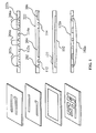
- FIG. 1 depicts a diagram of a first embodiment to decrease warpage of a multi-layer substrate according to the present invention.
- a three dimensional view of a multi-layer substrate is shown and a corresponding profile drawing is shown on the right side.
- the multi-layer substrate comprises a first metal layer 102, a first dielectric layer 122 corresponding thereto, second metal layers 112, 114 and a second dielectric layer 222 corresponding thereto.
- the first dielectric layer 122 and the second dielectric layer 222 are formed by a coating method.
- the aforesaid drying and hardening process is proceeded, and shrinkage rates of respective dielectric layers may be different. Stresses become unbalanced between some metal layers and dielectric layers to result in warpage of the multi-layer substrate.
- unbalanced stress between the metal layers and dielectric layers of the multi-layer substrate are making warpage thereof to happen because of different volumes, thicknesses, materials, or constructions of different metal layers and dielectric layers. Therefore, the present invention can be employed to homogenize the multi-layer structure composed of different metal layers and dielectric layers as shown in FIG. 1 .
- redundant metal layers 202, 204 and 206 can be set on the premise that circuit design is not affected.
- the second area plus the redundant metal layer area is considerably equivalent to the first area.
- the redundant metal layers 202, 204 and 206 and the second metal layer 112, 114 are positioned corresponding to the first metal layer 102 which is subject to a hypothetical central plane which is parallel with the first metal layer 102 and the second metal layer 112, 114. Accordingly, stress of the multi-layer substrate can be balanced to prevent warpage happening.
- the multi-layer substrate may further comprise a fourth metal layer 102a, a fourth dielectric layer 122a corresponding thereto, fifth metal layers 112a, 114a and fifth dielectric layer 222a corresponding thereto.
- the fourth metal layer 102a is located at outer side of the first metal layer 102; the fifth metal layers 112a, 114a are located at outer side of the second metal layers 112 and 114. As the fourth metal layer 102a is larger then the fifth metal layers 112a, 114a.
- fifth redundant metal layers 202a, 204a and 206a can be set in the same layer of the fifth metal layers 112a, 114a on the premise that circuit design is not affected.
- the fifth redundant metal layer area plus the fifth area is considerably equivalent to the fourth area.
- the fifth redundant metal layers 202a, 204a and 206a and the fifth metal layers 112a, 114a are positioned corresponding to the fourth metal layer 102a which is subject to a hypothetical central plane which is parallel with the fourth metal layer 102a and the fifth metal layers 112a, 114a.
- the two metal layers positioned corresponding to each other are adjacent with each other or not, making the inner of the multi-layer substrate as symmetrical structures described as the first metal layer 102 and the second metal layer 112, 114; as the fourth metal layer 102a and the fifth metal layers 112a, 114a, stresses of the multi-layer substrate can be balanced to decrease warpage thereof.
- the present invention can still work for balancing stress of the multi-layer substrate, therefore, decreasing warpage of the multi-layer substrate.
- FIG. 2 depicts a diagram of a second embodiment to decrease warpage of a multi-layer substrate according to the present invention.
- a three dimensional view of a multi-layer substrate is shown and a corresponding profile drawing is shown on the right side.
- the multi-layer substrate comprises a first metal layer 102, a first dielectric layer 122 corresponding thereto, second metal layers 112, 114 and a second dielectric layer 222 corresponding thereto.
- pattern of the first metal layer 102 is complex but occupied area thereof is still larger than area of the second metal layers 112, 114. Therefore, in the same layer of the second metal layers 112 and 114, small, distributed redundant metal layers 202, 204 and 206 can be set on the premise that circuit design is not affected. The purpose is that the redundant metal layer area plus the second area remains considerably equivalent to the first area. Moreover, the redundant metal layers 202, 204 and 206 and the second metal layer 112, 114 are positioned corresponding to the first metal layer 102 which is subject to a hypothetical central plane which is parallel with the first metal layer 102 and the second metal layer 112, 114. Accordingly, stress of the multi-layer substrate can be balanced to decrease warpage happening.
- FIG. 3 depicts a diagram of a third embodiment to decrease warpage of a multi-layer substrate according to the present invention.
- a three dimensional view of a multi-layer substrate is shown and a corresponding profile drawing is shown on the right side.
- the multi-layer substrate comprises a first metal layer 102, a first dielectric layer 122 corresponding thereto, second metal layers 112, 114 and a second dielectric layer 222 corresponding thereto.
- the multi-layer substrate can further comprise a third metal layer 302 and a third dielectric layer 322 corresponding thereto between the first metal layer 102 and the second metal layers 112, 114.
- the occupied area of the third metal layer 302 can be smaller than both areas of the first metal layer 102 and the second metal layers 112, 114. Therefore, consideration of area of the third metal layer 302 therebetween can be ignored but occupied areas locations differences of the first metal layer 102 and the second metal layers 112, 114.
- the present invention can set smaller redundant metal layers 202, 206 and a larger redundant metal layer 204 in the same layer of the second metal layers 112 and 114 on the premise that circuit design is not affected.
- the purpose is that the redundant metal layer area plus the second area remains considerably equivalent to the first area.
- the redundant metal layers 202, 204 and 206 and the second metal layer 112, 114 are positioned corresponding to the first metal layer 102 which is subject to a hypothetical central plane which is parallel with the first metal layer 102 and the second metal layer 112, 114. Accordingly, stress of the multi-layer substrate can be balanced to prevent warpage happening.
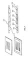
- FIG. 4 depicts a diagram of a fourth embodiment to decrease warpage of a multi-layer substrate according to the present invention. Similarly, on the left side of FIG. 4 , a three dimensional view of a multi-layer substrate is shown and a corresponding profile drawing is shown on the right side.
- the multi-layer substrate comprises a first metal layer 102, a first dielectric layer 122 corresponding thereto, second metal layers 112, 114 and a second dielectric layer 222 corresponding thereto.
- Occupied area of the first metal layer 102 is larger than area of the second metal layers 112, 114.
- redundant spaces 402, 404, 406, 408 and 410 can be set in the first metal layer 102 so that first area of the first metal layer 102 subtracting redundant space areas is considerably equivalent to the second area of the second metal layers 112, 114.
- the first metal layer 102 subtracting redundant spaces is positioned corresponding to the second metal layer 112 which is subject to a hypothetical central plane which is parallel with the first metal layer 102 and the second metal layer 112. Accordingly, balancing stress of the multi-layer substrate to decrease warpage thereof can be realized.
- the multi-layer substrate may further comprise a fourth metal layer located at inner side or outer side of the of the first metal layer 102; and, the fifth metal layer located at inner side or outer side of the second metal layers 112 and 114.
- the fourth metal layer is larger then the fifth metal layers.
- a fourth redundant space can be set in the fourth metal layer to make the inner of the multi-layer substrate as symmetrical structures. No matter corresponding metal layers are adjacent or not, stress of the multi-layer substrate can be balanced and warpage happening to the multi-layer substrate can be decreased.
- FIG. 5 depicts a diagram of a fifth embodiment to decrease warpage of a multi-layer substrate according to the present invention.
- the multi-layer substrate has an opening 502 in the first surface dielectric layer 522 located at a first surface of the multi-layer substrate at the position of a pad 500.
- the multi-layer substrate also has a second surface dielectric layer 524 located at a second surface of the multi-layer substrate.
- a redundant opening 602 can be set corresponding to the opening 502 positionally to balance stress of the multi-layer substrate to decrease warpage thereof.
- a redundant opening positioned corresponding to the opening 502 still can be set with overall considering the structure of the multi-layer substrate.
- the stress of the multi-layer substrate still can be balanced and decreasing warpage of the multi-layer substrate still can be realized.
- the first to fifth embodiments can be exercised alone or in combination for matching different electric circuit designs when a multi-layer substrate is manufactured. Homogenization for occupied areas and locations of different metal layers and dielectric layers in the multi-layer substrate can be achieved to decrease warpage or twist of the multi-layer substrate.
Landscapes
- Engineering & Computer Science (AREA)
- Microelectronics & Electronic Packaging (AREA)
- Physics & Mathematics (AREA)
- Electromagnetism (AREA)
- Production Of Multi-Layered Print Wiring Board (AREA)
- Structure Of Printed Boards (AREA)
Abstract
Description
- The present invention generally relates to a method to decrease warpage of a multi-layer substrate, and more particularly to a method of balancing a flexible multi-layer substrate stress to decrease warpage or twist of the multi-layer substrate for stresses generated by occupied area differences and occupied location differences of different metal layers and dielectric layers.
- A multi-layer substrate today may employ coating method to form a plurality of dielectric layers and corresponding metal layers between these dielectric layers are formed by lithography process. The aforesaid dielectric layers and metal layers are alternately stacked-up to realize the aforementioned multi-layer substrate having advantage of thin thickness and simple materials. Moreover, such coating method can be significantly suitable for manufacturing flexible multi-layer substrate.
- The wet films were formed by the dielectric layers coating method, therefore, the steps of drying these dielectric layers to be hardened thereof, are needed hereafter. Different metal layers have different areas and different locations because of respective circuit designs. Accordingly, dielectric layers corresponding to different metal layers may have different areas, also. After the metal layers and the dielectric layers are stacked-up and the aforesaid drying and hardening process are proceeded, shrinkage rates of respective dielectric layers may be different (although all dielectric layers' materials are the same, the shrinkage rates can be different due to respective shapes, occupied areas and volumes). Consequently, stresses become unbalanced between some metal layers and some dielectric layers to result in warpage or twist of the multi-layer substrate. Even the dielectric layers that are not formed by the coating method, unbalanced stress can cause warpage or twist of the multi-layer substrate that happens because of different volumes, thicknesses materials, or constructions of different metal layers and dielectric layers.
- The aforesaid warpage or twist can seriously influence precision of whole system assembly later on, even unable to assembly the whole system. Furthermore, speaking of design application of a flexible multi-layer substrate, foldable characteristic is the major purpose of developing the flexible multi-layer substrate industry. After the flexible multi-layer substrate is applied into productions, some specific areas, even the entire substrate can be bent frequently. If the stress, warpage or twist problems of the multi-layer substrate are not solved, the lifetime of the production can be shorter and cannot be commercialized.
- An objective of the present invention is to provide a method to decrease warpage of a multi-layer substrate by balancing a multi-layer substrate stress generated by occupied area differences and occupied location differences of different metal layers and dielectric layers.
- For accomplishing aforesaid objective of the present invention, the present invention employs to a multi-layer substrate having a first metal layer and a second metal layer at least and a first area of the first metal layer is larger than a second area of the second metal layer, wherein at least one redundant metal layer is set in the same layer of the second metal layer so that a redundant metal layer area plus the second area is considerably equivalent to the first area. The redundant metal layer and the second metal layer are positioned corresponding to the first metal layer which is subject to a central plane which is parallel with the first metal layer and the second metal layer. Furthermore, the method to decrease warpage according to the present invention can still be functional when a third metal layer is located between the first metal layer and the second metal layer.
- Moreover, when a first surface dielectric layer located at a first surface of the multi-layer substrate has at least one opening, the second surface dielectric layer located at a second surface of the multi-layer substrate can be set at least one redundant opening positioned corresponding to the at least one opening. According to the present invention, stresses caused by different occupied areas and locations of different metal layers and dielectric layers can be balanced, i.e. homogenizing occupied areas and locations of different metal layers and dielectric layers to decrease warpage or twist of the multi-layer substrate.
-
-
FIG. 1 depicts a diagram of a first embodiment to decrease warpage of a multi-layer substrate according to the present invention. -
FIG. 2 depicts a diagram of a second embodiment to decrease warpage of a multi-layer substrate according to the present invention. -
FIG. 3 depicts a diagram of a third embodiment to decrease warpage of a multi-layer substrate according to the present invention. -
FIG. 4 depicts a diagram of a fourth embodiment to decrease warpage of a multi-layer substrate according to the present invention. -
FIG. 5 depicts a diagram of a fifth embodiment to decrease warpage of a multi-layer substrate according to the present invention. - Please refer to
FIG. 1 , which depicts a diagram of a first embodiment to decrease warpage of a multi-layer substrate according to the present invention. On the left side ofFIG. 1 , a three dimensional view of a multi-layer substrate is shown and a corresponding profile drawing is shown on the right side. The multi-layer substrate comprises afirst metal layer 102, a firstdielectric layer 122 corresponding thereto,second metal layers dielectric layer 222 corresponding thereto. - As aforementioned, the first
dielectric layer 122 and the seconddielectric layer 222 are formed by a coating method. The aforesaid drying and hardening process is proceeded, and shrinkage rates of respective dielectric layers may be different. Stresses become unbalanced between some metal layers and dielectric layers to result in warpage of the multi-layer substrate. Moreover, even the dielectric layers are not formed by the coating method, unbalanced stress between the metal layers and dielectric layers of the multi-layer substrate are making warpage thereof to happen because of different volumes, thicknesses, materials, or constructions of different metal layers and dielectric layers. Therefore, the present invention can be employed to homogenize the multi-layer structure composed of different metal layers and dielectric layers as shown inFIG. 1 . - Because an area of the
first metal layer 102 occupies most of the multi-layer substrate and is larger than an area of thesecond metal layers second metal layers redundant metal layers redundant metal layers second metal layer first metal layer 102 which is subject to a hypothetical central plane which is parallel with thefirst metal layer 102 and thesecond metal layer - As shown in
FIG. 1 , the multi-layer substrate may further comprise afourth metal layer 102a, a fourthdielectric layer 122a corresponding thereto,fifth metal layers dielectric layer 222a corresponding thereto. Thefourth metal layer 102a is located at outer side of thefirst metal layer 102; thefifth metal layers second metal layers fourth metal layer 102a is larger then thefifth metal layers redundant metal layers fifth metal layers redundant metal layers fifth metal layers fourth metal layer 102a which is subject to a hypothetical central plane which is parallel with thefourth metal layer 102a and thefifth metal layers - With overall consideration for the multi-layer substrate, no matter the two metal layers positioned corresponding to each other are adjacent with each other or not, making the inner of the multi-layer substrate as symmetrical structures described as the
first metal layer 102 and thesecond metal layer fourth metal layer 102a and thefifth metal layers fourth metal layer 102a is located at inner side of thefirst metal layer 102; thefifth metal layers second metal layers - Please refer to
FIG. 2 , which depicts a diagram of a second embodiment to decrease warpage of a multi-layer substrate according to the present invention. Similarly, on the left side ofFIG. 2 , a three dimensional view of a multi-layer substrate is shown and a corresponding profile drawing is shown on the right side. The multi-layer substrate comprises afirst metal layer 102, a firstdielectric layer 122 corresponding thereto,second metal layers dielectric layer 222 corresponding thereto. - In this embodiment, pattern of the
first metal layer 102 is complex but occupied area thereof is still larger than area of thesecond metal layers second metal layers redundant metal layers redundant metal layers second metal layer first metal layer 102 which is subject to a hypothetical central plane which is parallel with thefirst metal layer 102 and thesecond metal layer - Please refer to
FIG. 3 , which depicts a diagram of a third embodiment to decrease warpage of a multi-layer substrate according to the present invention. Similarly, on the left side ofFIG. 3 , a three dimensional view of a multi-layer substrate is shown and a corresponding profile drawing is shown on the right side. The multi-layer substrate comprises afirst metal layer 102, a firstdielectric layer 122 corresponding thereto,second metal layers dielectric layer 222 corresponding thereto. - Furthermore, the multi-layer substrate can further comprise a
third metal layer 302 and a thirddielectric layer 322 corresponding thereto between thefirst metal layer 102 and thesecond metal layers third metal layer 302 can be smaller than both areas of thefirst metal layer 102 and the second metal layers 112, 114. Therefore, consideration of area of thethird metal layer 302 therebetween can be ignored but occupied areas locations differences of thefirst metal layer 102 and the second metal layers 112, 114. - As aforementioned, as making the inner of the multi-layer substrate as symmetrical structures with overall considering the multi-layer substrate, therefore, the present invention can set smaller
redundant metal layers redundant metal layer 204 in the same layer of thesecond metal layers redundant metal layers second metal layer first metal layer 102 which is subject to a hypothetical central plane which is parallel with thefirst metal layer 102 and thesecond metal layer - Please refer to
FIG. 4 , which depicts a diagram of a fourth embodiment to decrease warpage of a multi-layer substrate according to the present invention. Similarly, on the left side ofFIG. 4 , a three dimensional view of a multi-layer substrate is shown and a corresponding profile drawing is shown on the right side. The multi-layer substrate comprises afirst metal layer 102, a firstdielectric layer 122 corresponding thereto, second metal layers 112, 114 and asecond dielectric layer 222 corresponding thereto. - Occupied area of the
first metal layer 102 is larger than area of the second metal layers 112, 114. However, what is different from the aforesaid embodiments is thatredundant spaces first metal layer 102 so that first area of thefirst metal layer 102 subtracting redundant space areas is considerably equivalent to the second area of the second metal layers 112, 114. Besides, thefirst metal layer 102 subtracting redundant spaces is positioned corresponding to thesecond metal layer 112 which is subject to a hypothetical central plane which is parallel with thefirst metal layer 102 and thesecond metal layer 112. Accordingly, balancing stress of the multi-layer substrate to decrease warpage thereof can be realized. In this embodiment, certainly as similar as described in aforesaid embodiment, the multi-layer substrate may further comprise a fourth metal layer located at inner side or outer side of the of thefirst metal layer 102; and, the fifth metal layer located at inner side or outer side of thesecond metal layers - Please refer to
FIG. 5 , which depicts a diagram of a fifth embodiment to decrease warpage of a multi-layer substrate according to the present invention. As shown inFIG. 5 , the multi-layer substrate has anopening 502 in the firstsurface dielectric layer 522 located at a first surface of the multi-layer substrate at the position of apad 500. The multi-layer substrate also has a secondsurface dielectric layer 524 located at a second surface of the multi-layer substrate. With concept of homogenize the multi-layer structure composed of different metal layers and dielectric layers according to the present invention, aredundant opening 602 can be set corresponding to theopening 502 positionally to balance stress of the multi-layer substrate to decrease warpage thereof. Similarly, if theopening 502 is in the inner of the multi-layer substrate, a redundant opening positioned corresponding to theopening 502 still can be set with overall considering the structure of the multi-layer substrate. The stress of the multi-layer substrate still can be balanced and decreasing warpage of the multi-layer substrate still can be realized. - In conclusion, the first to fifth embodiments can be exercised alone or in combination for matching different electric circuit designs when a multi-layer substrate is manufactured. Homogenization for occupied areas and locations of different metal layers and dielectric layers in the multi-layer substrate can be achieved to decrease warpage or twist of the multi-layer substrate.
- As is understood by a person skilled in the art, the foregoing preferred embodiments of the present invention are illustrative rather than limiting of the present invention. It is intended that they cover various modifications and similar arrangements be included within the spirit and scope of the appended claims, the scope of which should be accorded the broadest interpretation so as to encompass all such modifications and similar structure.
Claims (26)
- A method to decrease warpage of a multi-layer substrate, the multi-layer substrate comprising a first metal layer and a second metal layer, a first area of the first metal layer is larger than a second area of the second metal layer, wherein at least one redundant metal layer is set in the same layer of the second metal layer so that a redundant metal layer area plus the second area is considerably equivalent to the first area.
- The method of claim 1, wherein the redundant metal layer and the second metal layer are positioned corresponding to the first metal layer which is subject to a central plane which is parallel with the first metal layer and the second metal layer.
- The method of claim 1, wherein a third metal layer is located between the first metal layer and the second metal layer.
- The method of claim 1, wherein the multi-layer substrate further comprises a first surface dielectric layer located at a first surface of the multi-layer substrate that the first surface dielectric layer has at least one opening.
- The method of claim 4, wherein the multi-layer substrate further comprises a second surface dielectric layer located at a second surface of the multi-layer substrate that the second surface dielectric layer has at least one redundant opening positioned corresponding to the at least one opening.
- A method to decrease warpage of a multi-layer substrate, the multi-layer substrate comprising a first metal layer and a second metal layer, a first area of the first metal layer is larger than a second area of the second metal layer, wherein at least one redundant space is set in the first metal layer so that the first area subtracting a redundant space area is considerably equivalent to the second area.
- The method of claim 6, wherein the second metal layer is positioned corresponding to the first metal layer except the redundant space which is subject to a central plane which is parallel with the first metal layer and the second metal layer.
- The method of claim 6, wherein a third metal layer is located between the first metal layer and the second metal layer.
- The method of claim 6, wherein the multi-layer substrate further comprises a first surface dielectric layer located at a first surface of the multi-layer substrate that the first surface dielectric layer has at least one opening.
- The method of claim 9, wherein the multi-layer substrate further comprises a second surface dielectric layer located at a second surface of the multi-layer substrate that the second surface dielectric layer has at least one redundant opening positioned corresponding to the at least one opening.
- A method to decrease warpage of a multi-layer substrate, comprising a first surface dielectric layer located at a first surface of the multi-layer substrate that the first surface dielectric layer has at least one opening and a second surface dielectric layer located at a second surface of the multi-layer substrate, wherein the second surface dielectric layer has at least one redundant opening positioned corresponding to the at least one opening.
- A method to decrease warpage of a multi-layer substrate, comprising a first dielectric layer in the multi-layer substrate that the first dielectric layer has at least one opening and a second surface dielectric layer in the multi-layer substrate, wherein the second dielectric layer has at least one redundant opening positioned corresponding to the at least one opening.
- A multi-layer substrate structure, comprising a first metal layer and a second metal layer, a first area of the first metal layer is larger than a second area of the second metal layer, wherein at least one redundant metal layer is set in the same layer of the second metal layer so that a redundant metal layer area plus the second area is considerably equivalent to the first area.
- The multi-layer substrate structure of claim 13, wherein the redundant metal layer and the second metal layer are positioned corresponding to the first metal layer which is subject to a central plane which is parallel with the first metal layer and the second metal layer.
- The multi-layer substrate structure of claim 13, wherein a third metal layer is located between the first metal layer and the second metal layer.
- The multi-layer substrate structure of claim 13, wherein the multi-layer substrate further comprises a fourth metal layer and a fifth metal layer, located at outer sides of the first metal layer and the second metal layer respectively, a fourth area of the fourth metal layer is larger than a fifth area of the fifth metal layer, wherein at least one fifth redundant metal layer is set in the same layer of the fifth metal layer so that a fifth redundant metal layer area plus the fifth area is considerably equivalent to the fourth area.
- The multi-layer substrate structure of claim 16, wherein the fifth redundant metal layer and the fifth metal layer are positioned corresponding to the fourth metal layer subject to a central plane parallel with the fourth metal layer and the fifth metal layer.
- The multi-layer substrate structure of claim 13, wherein the multi-layer substrate further comprises a first surface dielectric layer located at a first surface of the multi-layer substrate that the first surface dielectric layer has at least one opening.
- The multi-layer substrate structure of claim 18, wherein the multi-layer substrate further comprises a second surface dielectric layer located at a second surface of the multi-layer substrate that the second surface dielectric layer has at least one redundant opening positioned corresponding to the at least one opening.
- A multi-layer substrate structure, comprising a first metal layer and a second metal layer, a first area of the first metal layer is larger than a second area of the second metal layer, wherein at least one redundant space is set in the first metal layer so that the first area subtracting a redundant space area is considerably equivalent to the second area.
- The multi-layer substrate structure of claim 20, wherein the second metal layer is positioned corresponding to the first metal layer except the redundant space which is subject to a central plane which is parallel with the first metal layer and the second metal layer.
- The multi-layer substrate structure of claim 20, wherein a third metal layer is located between the first metal layer and the second metal layer.
- The multi-layer substrate structure of claim 20, wherein the multi-layer substrate further comprises a fourth metal layer and a fifth metal layer, located at outer sides of the first metal layer and the second metal layer respectively, a fourth area of the fourth metal layer is larger than a fifth area of the fifth metal layer, wherein at least one fourth redundant space is set in the fourth metal layer so that the fourth area subtracting a fourth redundant space area is considerably equivalent to the fifth area.
- The multi-layer substrate structure of claim 23, wherein the fifth metal layer is positioned corresponding to the fourth metal layer except the fourth redundant space which is subject to a central plane which is parallel with the fourth metal layer and the fifth metal layer.
- The multi-layer substrate structure of claim 20, wherein the multi-layer substrate further comprises a first surface dielectric layer located at a first surface of the multi-layer substrate that the first surface dielectric layer has at least one opening.
- The multi-layer substrate structure of claim 25, wherein the multi-layer substrate further comprises a second surface dielectric layer located at a second surface of the multi-layer substrate that the second surface dielectric layer has at least one redundant opening positioned corresponding to the at least one opening.
Applications Claiming Priority (1)
| Application Number | Priority Date | Filing Date | Title |
|---|---|---|---|
| PCT/CN2008/000630 WO2009121200A1 (en) | 2008-03-31 | 2008-03-31 | Method of balancing multilayer substrate stress and multilayer substrate |
Publications (3)
| Publication Number | Publication Date |
|---|---|
| EP2270851A1 true EP2270851A1 (en) | 2011-01-05 |
| EP2270851A4 EP2270851A4 (en) | 2011-06-29 |
| EP2270851B1 EP2270851B1 (en) | 2016-12-28 |
Family
ID=41134788
Family Applications (1)
| Application Number | Title | Priority Date | Filing Date |
|---|---|---|---|
| EP08733855.4A Not-in-force EP2270851B1 (en) | 2008-03-31 | 2008-03-31 | Method of balancing multilayer substrate stress and multilayer substrate |
Country Status (4)
| Country | Link |
|---|---|
| EP (1) | EP2270851B1 (en) |
| JP (1) | JP5404763B2 (en) |
| KR (1) | KR101229956B1 (en) |
| WO (1) | WO2009121200A1 (en) |
Cited By (1)
| Publication number | Priority date | Publication date | Assignee | Title |
|---|---|---|---|---|
| CN113518503A (en) * | 2021-03-31 | 2021-10-19 | 深圳市景旺电子股份有限公司 | Multilayer printed wiring board and method for manufacturing same |
Family Cites Families (18)
| Publication number | Priority date | Publication date | Assignee | Title |
|---|---|---|---|---|
| JPH0513957A (en) * | 1991-07-02 | 1993-01-22 | Mitsubishi Electric Corp | Printed wiring board |
| JPH06252556A (en) * | 1993-02-24 | 1994-09-09 | Mitsubishi Electric Corp | Multilayered ceramic substrate |
| JP2599674Y2 (en) * | 1993-12-28 | 1999-09-13 | 株式会社ミツバ | Pattern structure for noise suppression of substrate |
| JPH08288316A (en) * | 1995-04-14 | 1996-11-01 | Citizen Watch Co Ltd | Semiconductor device |
| US5888630A (en) * | 1996-11-08 | 1999-03-30 | W. L. Gore & Associates, Inc. | Apparatus and method for unit area composition control to minimize warp in an integrated circuit chip package assembly |
| JPH1117064A (en) * | 1997-06-24 | 1999-01-22 | Toshiba Corp | Semiconductor package |
| US6380633B1 (en) * | 2000-07-05 | 2002-04-30 | Siliconware Predision Industries Co., Ltd. | Pattern layout structure in substrate |
| JP2001068860A (en) * | 2000-08-07 | 2001-03-16 | Ibiden Co Ltd | Multilayer printed wiring board |
| JP2002261402A (en) * | 2001-03-01 | 2002-09-13 | Alps Electric Co Ltd | Circuit board for electronic circuit unit |
| JP2003218279A (en) * | 2002-01-23 | 2003-07-31 | Shinko Electric Ind Co Ltd | Circuit board and method of manufacturing the same |
| CN1199271C (en) * | 2002-08-28 | 2005-04-27 | 威盛电子股份有限公司 | Fabricated integrated circuits with balanced structures |
| CN1276504C (en) * | 2002-10-30 | 2006-09-20 | 矽品精密工业股份有限公司 | A substrate for preventing warpage |
| JP2004200265A (en) * | 2002-12-17 | 2004-07-15 | Nikon Corp | Printed wiring board |
| JP3918101B2 (en) * | 2004-04-06 | 2007-05-23 | 株式会社村田製作所 | Internal conductor connection structure and multilayer board |
| US7576013B2 (en) * | 2004-07-27 | 2009-08-18 | United Microelectronics Corp. | Method of relieving wafer stress |
| CN100388447C (en) * | 2004-12-20 | 2008-05-14 | 全懋精密科技股份有限公司 | Chip embedded substrate structure of semiconductor package and manufacturing method thereof |
| KR20070046422A (en) * | 2005-10-31 | 2007-05-03 | 엘지이노텍 주식회사 | Mounting pad for low temperature cofired ceramic multilayer |
| JP2008071963A (en) * | 2006-09-14 | 2008-03-27 | Denso Corp | Multilayer wiring board |
-
2008
- 2008-03-31 EP EP08733855.4A patent/EP2270851B1/en not_active Not-in-force
- 2008-03-31 WO PCT/CN2008/000630 patent/WO2009121200A1/en not_active Ceased
- 2008-03-31 KR KR1020107018159A patent/KR101229956B1/en not_active Expired - Fee Related
- 2008-03-31 JP JP2011501082A patent/JP5404763B2/en active Active
Cited By (2)
| Publication number | Priority date | Publication date | Assignee | Title |
|---|---|---|---|---|
| CN113518503A (en) * | 2021-03-31 | 2021-10-19 | 深圳市景旺电子股份有限公司 | Multilayer printed wiring board and method for manufacturing same |
| CN113518503B (en) * | 2021-03-31 | 2022-08-09 | 深圳市景旺电子股份有限公司 | Multilayer printed wiring board and method for manufacturing same |
Also Published As
| Publication number | Publication date |
|---|---|
| KR20110003316A (en) | 2011-01-11 |
| JP2011517063A (en) | 2011-05-26 |
| EP2270851B1 (en) | 2016-12-28 |
| EP2270851A4 (en) | 2011-06-29 |
| JP5404763B2 (en) | 2014-02-05 |
| KR101229956B1 (en) | 2013-02-06 |
| WO2009121200A1 (en) | 2009-10-08 |
Similar Documents
| Publication | Publication Date | Title |
|---|---|---|
| CN101151943A (en) | Rigid-flexible printed circuit board | |
| CN103996533B (en) | multilayer ceramic device | |
| US9378891B2 (en) | Multilayer ceramic device | |
| KR101514509B1 (en) | Multilayer ceramic device | |
| CN105552225B (en) | Method for manufacturing flexible substrate, and display device | |
| EP2270851B1 (en) | Method of balancing multilayer substrate stress and multilayer substrate | |
| CN105979698A (en) | Rigid-flex circuit board and preparation method thereof | |
| KR101655928B1 (en) | Method of manufacturing a printed circuit board | |
| US20100104889A1 (en) | Method to decrease warpage of multi-layer substrate and structure thereof | |
| CN101547570B (en) | Method for balancing stress of multilayer substrate and multilayer substrate | |
| KR102111529B1 (en) | Method for build-up of printed circuit board | |
| KR101951654B1 (en) | Manufacturing Method of Printed Circuit Board to Improve Flatness | |
| US20110212307A1 (en) | Method to decrease warpage of a multi-layer substrate and structure thereof | |
| JP2003133733A (en) | Flexible printed board provided with cable part | |
| JP2638555B2 (en) | Multilayer printed wiring board | |
| US20110212257A1 (en) | Method to decrease warpage of a multi-layer substrate and structure thereof | |
| CN117995527A (en) | Inductor component | |
| KR101811423B1 (en) | The method of menufacturing build-up layer of pcb | |
| CN205149058U (en) | Prevent off normal laminate assembly | |
| JP2013008910A (en) | Wiring board and method for manufacturing wiring board | |
| US20250203785A1 (en) | Circuit board structure and manufacturing method thereof | |
| CN120676559A (en) | Design method and manufacturing method of PCB with multiple blind buried holes and PCB | |
| KR101504543B1 (en) | Mask for forming pattern with double structure and method of manufacturing this | |
| EP3667466B1 (en) | Input device and manufacturing method for input device in which plastic cover and film sensor are stacked | |
| US20230284394A1 (en) | Method for producing wiring circuit board |
Legal Events
| Date | Code | Title | Description |
|---|---|---|---|
| PUAI | Public reference made under article 153(3) epc to a published international application that has entered the european phase |
Free format text: ORIGINAL CODE: 0009012 |
|
| 17P | Request for examination filed |
Effective date: 20100813 |
|
| AK | Designated contracting states |
Kind code of ref document: A1 Designated state(s): AT BE BG CH CY CZ DE DK EE ES FI FR GB GR HR HU IE IS IT LI LT LU LV MC MT NL NO PL PT RO SE SI SK TR |
|
| AX | Request for extension of the european patent |
Extension state: AL BA MK RS |
|
| REG | Reference to a national code |
Ref document number: 602008048121 Country of ref document: DE Ref country code: DE Ref legal event code: R079 Free format text: PREVIOUS MAIN CLASS: H01L0023120000 Ipc: H05K0001020000 |
|
| A4 | Supplementary search report drawn up and despatched |
Effective date: 20110526 |
|
| RIC1 | Information provided on ipc code assigned before grant |
Ipc: B32B 9/00 20060101ALI20110520BHEP Ipc: H05K 1/02 20060101AFI20110520BHEP Ipc: H01L 23/12 20060101ALI20110520BHEP |
|
| DAX | Request for extension of the european patent (deleted) | ||
| 17Q | First examination report despatched |
Effective date: 20120619 |
|
| RIC1 | Information provided on ipc code assigned before grant |
Ipc: H05K 3/46 20060101ALN20160706BHEP Ipc: H05K 1/02 20060101AFI20160706BHEP |
|
| GRAP | Despatch of communication of intention to grant a patent |
Free format text: ORIGINAL CODE: EPIDOSNIGR1 |
|
| INTG | Intention to grant announced |
Effective date: 20160812 |
|
| GRAS | Grant fee paid |
Free format text: ORIGINAL CODE: EPIDOSNIGR3 |
|
| GRAA | (expected) grant |
Free format text: ORIGINAL CODE: 0009210 |
|
| AK | Designated contracting states |
Kind code of ref document: B1 Designated state(s): AT BE BG CH CY CZ DE DK EE ES FI FR GB GR HR HU IE IS IT LI LT LU LV MC MT NL NO PL PT RO SE SI SK TR |
|
| REG | Reference to a national code |
Ref country code: GB Ref legal event code: FG4D |
|
| REG | Reference to a national code |
Ref country code: CH Ref legal event code: EP |
|
| REG | Reference to a national code |
Ref country code: AT Ref legal event code: REF Ref document number: 858272 Country of ref document: AT Kind code of ref document: T Effective date: 20170115 |
|
| REG | Reference to a national code |
Ref country code: IE Ref legal event code: FG4D |
|
| REG | Reference to a national code |
Ref country code: DE Ref legal event code: R096 Ref document number: 602008048121 Country of ref document: DE |
|
| PG25 | Lapsed in a contracting state [announced via postgrant information from national office to epo] |
Ref country code: LV Free format text: LAPSE BECAUSE OF FAILURE TO SUBMIT A TRANSLATION OF THE DESCRIPTION OR TO PAY THE FEE WITHIN THE PRESCRIBED TIME-LIMIT Effective date: 20161228 |
|
| REG | Reference to a national code |
Ref country code: NL Ref legal event code: FP |
|
| REG | Reference to a national code |
Ref country code: LT Ref legal event code: MG4D |
|
| PG25 | Lapsed in a contracting state [announced via postgrant information from national office to epo] |
Ref country code: GR Free format text: LAPSE BECAUSE OF FAILURE TO SUBMIT A TRANSLATION OF THE DESCRIPTION OR TO PAY THE FEE WITHIN THE PRESCRIBED TIME-LIMIT Effective date: 20170329 Ref country code: SE Free format text: LAPSE BECAUSE OF FAILURE TO SUBMIT A TRANSLATION OF THE DESCRIPTION OR TO PAY THE FEE WITHIN THE PRESCRIBED TIME-LIMIT Effective date: 20161228 Ref country code: NO Free format text: LAPSE BECAUSE OF FAILURE TO SUBMIT A TRANSLATION OF THE DESCRIPTION OR TO PAY THE FEE WITHIN THE PRESCRIBED TIME-LIMIT Effective date: 20170328 Ref country code: LT Free format text: LAPSE BECAUSE OF FAILURE TO SUBMIT A TRANSLATION OF THE DESCRIPTION OR TO PAY THE FEE WITHIN THE PRESCRIBED TIME-LIMIT Effective date: 20161228 |
|
| REG | Reference to a national code |
Ref country code: AT Ref legal event code: MK05 Ref document number: 858272 Country of ref document: AT Kind code of ref document: T Effective date: 20161228 |
|
| PG25 | Lapsed in a contracting state [announced via postgrant information from national office to epo] |
Ref country code: HR Free format text: LAPSE BECAUSE OF FAILURE TO SUBMIT A TRANSLATION OF THE DESCRIPTION OR TO PAY THE FEE WITHIN THE PRESCRIBED TIME-LIMIT Effective date: 20161228 Ref country code: FI Free format text: LAPSE BECAUSE OF FAILURE TO SUBMIT A TRANSLATION OF THE DESCRIPTION OR TO PAY THE FEE WITHIN THE PRESCRIBED TIME-LIMIT Effective date: 20161228 |
|
| PG25 | Lapsed in a contracting state [announced via postgrant information from national office to epo] |
Ref country code: SK Free format text: LAPSE BECAUSE OF FAILURE TO SUBMIT A TRANSLATION OF THE DESCRIPTION OR TO PAY THE FEE WITHIN THE PRESCRIBED TIME-LIMIT Effective date: 20161228 Ref country code: IS Free format text: LAPSE BECAUSE OF FAILURE TO SUBMIT A TRANSLATION OF THE DESCRIPTION OR TO PAY THE FEE WITHIN THE PRESCRIBED TIME-LIMIT Effective date: 20170428 Ref country code: CZ Free format text: LAPSE BECAUSE OF FAILURE TO SUBMIT A TRANSLATION OF THE DESCRIPTION OR TO PAY THE FEE WITHIN THE PRESCRIBED TIME-LIMIT Effective date: 20161228 Ref country code: EE Free format text: LAPSE BECAUSE OF FAILURE TO SUBMIT A TRANSLATION OF THE DESCRIPTION OR TO PAY THE FEE WITHIN THE PRESCRIBED TIME-LIMIT Effective date: 20161228 Ref country code: RO Free format text: LAPSE BECAUSE OF FAILURE TO SUBMIT A TRANSLATION OF THE DESCRIPTION OR TO PAY THE FEE WITHIN THE PRESCRIBED TIME-LIMIT Effective date: 20161228 |
|
| PG25 | Lapsed in a contracting state [announced via postgrant information from national office to epo] |
Ref country code: BE Free format text: LAPSE BECAUSE OF FAILURE TO SUBMIT A TRANSLATION OF THE DESCRIPTION OR TO PAY THE FEE WITHIN THE PRESCRIBED TIME-LIMIT Effective date: 20161228 Ref country code: ES Free format text: LAPSE BECAUSE OF FAILURE TO SUBMIT A TRANSLATION OF THE DESCRIPTION OR TO PAY THE FEE WITHIN THE PRESCRIBED TIME-LIMIT Effective date: 20161228 Ref country code: BG Free format text: LAPSE BECAUSE OF FAILURE TO SUBMIT A TRANSLATION OF THE DESCRIPTION OR TO PAY THE FEE WITHIN THE PRESCRIBED TIME-LIMIT Effective date: 20170328 Ref country code: PT Free format text: LAPSE BECAUSE OF FAILURE TO SUBMIT A TRANSLATION OF THE DESCRIPTION OR TO PAY THE FEE WITHIN THE PRESCRIBED TIME-LIMIT Effective date: 20170428 Ref country code: AT Free format text: LAPSE BECAUSE OF FAILURE TO SUBMIT A TRANSLATION OF THE DESCRIPTION OR TO PAY THE FEE WITHIN THE PRESCRIBED TIME-LIMIT Effective date: 20161228 Ref country code: IT Free format text: LAPSE BECAUSE OF FAILURE TO SUBMIT A TRANSLATION OF THE DESCRIPTION OR TO PAY THE FEE WITHIN THE PRESCRIBED TIME-LIMIT Effective date: 20161228 Ref country code: PL Free format text: LAPSE BECAUSE OF FAILURE TO SUBMIT A TRANSLATION OF THE DESCRIPTION OR TO PAY THE FEE WITHIN THE PRESCRIBED TIME-LIMIT Effective date: 20161228 |
|
| REG | Reference to a national code |
Ref country code: DE Ref legal event code: R097 Ref document number: 602008048121 Country of ref document: DE |
|
| REG | Reference to a national code |
Ref country code: CH Ref legal event code: PL |
|
| PLBE | No opposition filed within time limit |
Free format text: ORIGINAL CODE: 0009261 |
|
| STAA | Information on the status of an ep patent application or granted ep patent |
Free format text: STATUS: NO OPPOSITION FILED WITHIN TIME LIMIT |
|
| PG25 | Lapsed in a contracting state [announced via postgrant information from national office to epo] |
Ref country code: DK Free format text: LAPSE BECAUSE OF FAILURE TO SUBMIT A TRANSLATION OF THE DESCRIPTION OR TO PAY THE FEE WITHIN THE PRESCRIBED TIME-LIMIT Effective date: 20161228 Ref country code: MC Free format text: LAPSE BECAUSE OF FAILURE TO SUBMIT A TRANSLATION OF THE DESCRIPTION OR TO PAY THE FEE WITHIN THE PRESCRIBED TIME-LIMIT Effective date: 20161228 |
|
| 26N | No opposition filed |
Effective date: 20170929 |
|
| REG | Reference to a national code |
Ref country code: IE Ref legal event code: MM4A |
|
| REG | Reference to a national code |
Ref country code: FR Ref legal event code: ST Effective date: 20171130 |
|
| PG25 | Lapsed in a contracting state [announced via postgrant information from national office to epo] |
Ref country code: FR Free format text: LAPSE BECAUSE OF NON-PAYMENT OF DUE FEES Effective date: 20170331 Ref country code: LU Free format text: LAPSE BECAUSE OF NON-PAYMENT OF DUE FEES Effective date: 20170331 |
|
| PG25 | Lapsed in a contracting state [announced via postgrant information from national office to epo] |
Ref country code: LI Free format text: LAPSE BECAUSE OF NON-PAYMENT OF DUE FEES Effective date: 20170331 Ref country code: SI Free format text: LAPSE BECAUSE OF FAILURE TO SUBMIT A TRANSLATION OF THE DESCRIPTION OR TO PAY THE FEE WITHIN THE PRESCRIBED TIME-LIMIT Effective date: 20161228 Ref country code: IE Free format text: LAPSE BECAUSE OF NON-PAYMENT OF DUE FEES Effective date: 20170331 Ref country code: CH Free format text: LAPSE BECAUSE OF NON-PAYMENT OF DUE FEES Effective date: 20170331 |
|
| PG25 | Lapsed in a contracting state [announced via postgrant information from national office to epo] |
Ref country code: MT Free format text: LAPSE BECAUSE OF NON-PAYMENT OF DUE FEES Effective date: 20170331 |
|
| PGFP | Annual fee paid to national office [announced via postgrant information from national office to epo] |
Ref country code: DE Payment date: 20190312 Year of fee payment: 12 Ref country code: GB Payment date: 20190320 Year of fee payment: 12 |
|
| PGFP | Annual fee paid to national office [announced via postgrant information from national office to epo] |
Ref country code: NL Payment date: 20190313 Year of fee payment: 12 |
|
| PG25 | Lapsed in a contracting state [announced via postgrant information from national office to epo] |
Ref country code: HU Free format text: LAPSE BECAUSE OF FAILURE TO SUBMIT A TRANSLATION OF THE DESCRIPTION OR TO PAY THE FEE WITHIN THE PRESCRIBED TIME-LIMIT; INVALID AB INITIO Effective date: 20080331 |
|
| PG25 | Lapsed in a contracting state [announced via postgrant information from national office to epo] |
Ref country code: CY Free format text: LAPSE BECAUSE OF NON-PAYMENT OF DUE FEES Effective date: 20161228 |
|
| PG25 | Lapsed in a contracting state [announced via postgrant information from national office to epo] |
Ref country code: TR Free format text: LAPSE BECAUSE OF FAILURE TO SUBMIT A TRANSLATION OF THE DESCRIPTION OR TO PAY THE FEE WITHIN THE PRESCRIBED TIME-LIMIT Effective date: 20161228 |
|
| REG | Reference to a national code |
Ref country code: DE Ref legal event code: R119 Ref document number: 602008048121 Country of ref document: DE |
|
| REG | Reference to a national code |
Ref country code: NL Ref legal event code: MM Effective date: 20200401 |
|
| PG25 | Lapsed in a contracting state [announced via postgrant information from national office to epo] |
Ref country code: NL Free format text: LAPSE BECAUSE OF NON-PAYMENT OF DUE FEES Effective date: 20200401 |
|
| PG25 | Lapsed in a contracting state [announced via postgrant information from national office to epo] |
Ref country code: DE Free format text: LAPSE BECAUSE OF NON-PAYMENT OF DUE FEES Effective date: 20201001 |
|
| GBPC | Gb: european patent ceased through non-payment of renewal fee |
Effective date: 20200331 |
|
| PG25 | Lapsed in a contracting state [announced via postgrant information from national office to epo] |
Ref country code: GB Free format text: LAPSE BECAUSE OF NON-PAYMENT OF DUE FEES Effective date: 20200331 |