EP2267923B1 - Optical transmission system - Google Patents
Optical transmission system Download PDFInfo
- Publication number
- EP2267923B1 EP2267923B1 EP10183485A EP10183485A EP2267923B1 EP 2267923 B1 EP2267923 B1 EP 2267923B1 EP 10183485 A EP10183485 A EP 10183485A EP 10183485 A EP10183485 A EP 10183485A EP 2267923 B1 EP2267923 B1 EP 2267923B1
- Authority
- EP
- European Patent Office
- Prior art keywords
- optical
- signal
- unit
- phase shift
- phase
- Prior art date
- Legal status (The legal status is an assumption and is not a legal conclusion. Google has not performed a legal analysis and makes no representation as to the accuracy of the status listed.)
- Expired - Fee Related
Links
- 230000003287 optical effect Effects 0.000 title claims description 266
- 230000005540 biological transmission Effects 0.000 title description 8
- 230000010363 phase shift Effects 0.000 claims description 183
- 230000008878 coupling Effects 0.000 claims description 7
- 238000010168 coupling process Methods 0.000 claims description 7
- 238000005859 coupling reaction Methods 0.000 claims description 7
- 230000010354 integration Effects 0.000 claims description 5
- 230000001419 dependent effect Effects 0.000 claims 1
- 238000010586 diagram Methods 0.000 description 41
- 238000012544 monitoring process Methods 0.000 description 32
- 238000001514 detection method Methods 0.000 description 15
- 238000000034 method Methods 0.000 description 12
- 238000000605 extraction Methods 0.000 description 9
- 238000004891 communication Methods 0.000 description 8
- 238000001228 spectrum Methods 0.000 description 7
- 238000004088 simulation Methods 0.000 description 6
- 239000013307 optical fiber Substances 0.000 description 5
- 230000007274 generation of a signal involved in cell-cell signaling Effects 0.000 description 4
- 230000001360 synchronised effect Effects 0.000 description 4
- 230000015556 catabolic process Effects 0.000 description 3
- 230000003247 decreasing effect Effects 0.000 description 3
- 238000006731 degradation reaction Methods 0.000 description 3
- 230000000694 effects Effects 0.000 description 3
- 230000010287 polarization Effects 0.000 description 3
- 230000000644 propagated effect Effects 0.000 description 3
- 230000006866 deterioration Effects 0.000 description 2
- 238000005516 engineering process Methods 0.000 description 2
- 239000000284 extract Substances 0.000 description 2
- 238000005070 sampling Methods 0.000 description 2
- 239000010409 thin film Substances 0.000 description 2
- 229910003327 LiNbO3 Inorganic materials 0.000 description 1
- 230000005697 Pockels effect Effects 0.000 description 1
- 230000002411 adverse Effects 0.000 description 1
- 238000013459 approach Methods 0.000 description 1
- 238000011161 development Methods 0.000 description 1
- 230000002349 favourable effect Effects 0.000 description 1
- 238000012986 modification Methods 0.000 description 1
- 230000004048 modification Effects 0.000 description 1
- 230000005693 optoelectronics Effects 0.000 description 1
- 230000000737 periodic effect Effects 0.000 description 1
- 230000001902 propagating effect Effects 0.000 description 1
- 230000002441 reversible effect Effects 0.000 description 1
- 239000004065 semiconductor Substances 0.000 description 1
Images


Classifications
-
- G—PHYSICS
- G02—OPTICS
- G02F—OPTICAL DEVICES OR ARRANGEMENTS FOR THE CONTROL OF LIGHT BY MODIFICATION OF THE OPTICAL PROPERTIES OF THE MEDIA OF THE ELEMENTS INVOLVED THEREIN; NON-LINEAR OPTICS; FREQUENCY-CHANGING OF LIGHT; OPTICAL LOGIC ELEMENTS; OPTICAL ANALOGUE/DIGITAL CONVERTERS
- G02F1/00—Devices or arrangements for the control of the intensity, colour, phase, polarisation or direction of light arriving from an independent light source, e.g. switching, gating or modulating; Non-linear optics
- G02F1/01—Devices or arrangements for the control of the intensity, colour, phase, polarisation or direction of light arriving from an independent light source, e.g. switching, gating or modulating; Non-linear optics for the control of the intensity, phase, polarisation or colour
- G02F1/0121—Operation of devices; Circuit arrangements, not otherwise provided for in this subclass
- G02F1/0123—Circuits for the control or stabilisation of the bias voltage, e.g. automatic bias control [ABC] feedback loops
-
- G—PHYSICS
- G02—OPTICS
- G02F—OPTICAL DEVICES OR ARRANGEMENTS FOR THE CONTROL OF LIGHT BY MODIFICATION OF THE OPTICAL PROPERTIES OF THE MEDIA OF THE ELEMENTS INVOLVED THEREIN; NON-LINEAR OPTICS; FREQUENCY-CHANGING OF LIGHT; OPTICAL LOGIC ELEMENTS; OPTICAL ANALOGUE/DIGITAL CONVERTERS
- G02F1/00—Devices or arrangements for the control of the intensity, colour, phase, polarisation or direction of light arriving from an independent light source, e.g. switching, gating or modulating; Non-linear optics
- G02F1/01—Devices or arrangements for the control of the intensity, colour, phase, polarisation or direction of light arriving from an independent light source, e.g. switching, gating or modulating; Non-linear optics for the control of the intensity, phase, polarisation or colour
- G02F1/21—Devices or arrangements for the control of the intensity, colour, phase, polarisation or direction of light arriving from an independent light source, e.g. switching, gating or modulating; Non-linear optics for the control of the intensity, phase, polarisation or colour by interference
- G02F1/225—Devices or arrangements for the control of the intensity, colour, phase, polarisation or direction of light arriving from an independent light source, e.g. switching, gating or modulating; Non-linear optics for the control of the intensity, phase, polarisation or colour by interference in an optical waveguide structure
- G02F1/2255—Devices or arrangements for the control of the intensity, colour, phase, polarisation or direction of light arriving from an independent light source, e.g. switching, gating or modulating; Non-linear optics for the control of the intensity, phase, polarisation or colour by interference in an optical waveguide structure controlled by a high-frequency electromagnetic component in an electric waveguide structure
-
- H—ELECTRICITY
- H04—ELECTRIC COMMUNICATION TECHNIQUE
- H04B—TRANSMISSION
- H04B10/00—Transmission systems employing electromagnetic waves other than radio-waves, e.g. infrared, visible or ultraviolet light, or employing corpuscular radiation, e.g. quantum communication
- H04B10/50—Transmitters
- H04B10/501—Structural aspects
- H04B10/503—Laser transmitters
- H04B10/505—Laser transmitters using external modulation
- H04B10/5051—Laser transmitters using external modulation using a series, i.e. cascade, combination of modulators
-
- H—ELECTRICITY
- H04—ELECTRIC COMMUNICATION TECHNIQUE
- H04B—TRANSMISSION
- H04B10/00—Transmission systems employing electromagnetic waves other than radio-waves, e.g. infrared, visible or ultraviolet light, or employing corpuscular radiation, e.g. quantum communication
- H04B10/50—Transmitters
- H04B10/501—Structural aspects
- H04B10/503—Laser transmitters
- H04B10/505—Laser transmitters using external modulation
- H04B10/5053—Laser transmitters using external modulation using a parallel, i.e. shunt, combination of modulators
-
- H—ELECTRICITY
- H04—ELECTRIC COMMUNICATION TECHNIQUE
- H04B—TRANSMISSION
- H04B10/00—Transmission systems employing electromagnetic waves other than radio-waves, e.g. infrared, visible or ultraviolet light, or employing corpuscular radiation, e.g. quantum communication
- H04B10/50—Transmitters
- H04B10/501—Structural aspects
- H04B10/503—Laser transmitters
- H04B10/505—Laser transmitters using external modulation
- H04B10/5057—Laser transmitters using external modulation using a feedback signal generated by analysing the optical output
- H04B10/50575—Laser transmitters using external modulation using a feedback signal generated by analysing the optical output to control the modulator DC bias
-
- H—ELECTRICITY
- H04—ELECTRIC COMMUNICATION TECHNIQUE
- H04B—TRANSMISSION
- H04B10/00—Transmission systems employing electromagnetic waves other than radio-waves, e.g. infrared, visible or ultraviolet light, or employing corpuscular radiation, e.g. quantum communication
- H04B10/50—Transmitters
- H04B10/501—Structural aspects
- H04B10/503—Laser transmitters
- H04B10/505—Laser transmitters using external modulation
- H04B10/5057—Laser transmitters using external modulation using a feedback signal generated by analysing the optical output
- H04B10/50577—Laser transmitters using external modulation using a feedback signal generated by analysing the optical output to control the phase of the modulating signal
-
- H—ELECTRICITY
- H04—ELECTRIC COMMUNICATION TECHNIQUE
- H04B—TRANSMISSION
- H04B10/00—Transmission systems employing electromagnetic waves other than radio-waves, e.g. infrared, visible or ultraviolet light, or employing corpuscular radiation, e.g. quantum communication
- H04B10/50—Transmitters
- H04B10/501—Structural aspects
- H04B10/503—Laser transmitters
- H04B10/505—Laser transmitters using external modulation
- H04B10/5059—Laser transmitters using external modulation using a feed-forward signal generated by analysing the optical or electrical input
- H04B10/50597—Laser transmitters using external modulation using a feed-forward signal generated by analysing the optical or electrical input to control the phase of the modulating signal
-
- H—ELECTRICITY
- H04—ELECTRIC COMMUNICATION TECHNIQUE
- H04B—TRANSMISSION
- H04B10/00—Transmission systems employing electromagnetic waves other than radio-waves, e.g. infrared, visible or ultraviolet light, or employing corpuscular radiation, e.g. quantum communication
- H04B10/50—Transmitters
- H04B10/58—Compensation for non-linear transmitter output
Definitions
- the present invention relates to an optical transmitting apparatus, and in particular, relates to optical transmitting apparatus for transmitting an optical signal using PSK modulation.
- optical transmitting apparatus aiming to establish a high capacity and long distance optical transmission system has been awaited in recent years.
- expectations for implementation of an optical transmitting apparatus, which employs an optical modulation technique adequate for high capacity and long-distance, to an actual system are growing high.
- optical transmission systems using phase shift keying such as DPSK (Differential Phase Shift Keying) and DQPSK (Differential Quadrature Phase Shift Keying) are envisioned.
- phase shift keying such as DPSK (Differential Phase Shift Keying) and DQPSK (Differential Quadrature Phase Shift Keying) are envisioned.
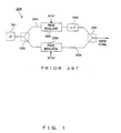
- Fig. 1 is a diagram showing a configuration of optical 1 transmitting apparatus, which is heretofore known, for transmitting a QPSK signal or a DQPSK signal.
- an optical source (LD) 2001 generates an optical continuous wave (CW).
- An optical splitter 2002 splits the optical CW and guides to arms 2003 and 2004.
- phase modulators 2005 and 2006 are configured respectively. Both phase modulators 2005 and 2006 are Mach-Zehnder interferometers.
- the phase modulator 2005 performs phase modulation of the optical CW using data 1
- the phase modulator 2006 performs phase modulation of the optical CW using data 2.
- DQPSK the data 1 and data 2 are encoded by a DQPSK pre-coder.
- An optical coupler 2007 couples modulated signals obtained from the phase modulators 2005 and 2006.
- a phase shifter 2008 causes the phase difference of ⁇ /2 between an optical signal guided to the optical coupler 2007 via the arm 2003 and an optical signal guided to the optical coupler 2007 via the arm 2004.
- a QPSK optical signal or a DQPSK optical signal is generated. Details of the configuration and the operation of DQPSK optical transmitting apparatus are described, for example, in Patent Document 1 (Japanese Patent Application Laid-open Publication No. 2004-516743 ( WO2002/051041 or US2004/0081470 )).
- Patent Document 2 Japanese Patent Application Laid-open Publication No. 2004-318052 . describes a technology for appropriately correcting DC bias in each optical modulator unit of SSB (Single Side-Band) optical modulator apparatus comprising a plurality of the optical modulator units, during normal operation of the modulator.
- SSB optical modulator apparatus also, a phase shifter for causing the phase difference of ⁇ /2 in optical signals propagated in a pair of arms is configured.
- Patent documents 3 Japanese Patent Application Laid-open Publication No. H03-251815
- Patent document 4 Japanese Patent Application Laid-open Publication No. H09-261207
- the amount of phase shift provided by the phase shifter 2008 ( ⁇ /2" in the QPSK and the DQPSK) to be set accurately to attain favorable reception quality.
- the amount of phase shift may sometimes deviate from a prescribed value due to thermal change and aged degradation etc.
- WO-A1-03/049333 discloses a modulator arrangement for modulating an optical signal using a quadrature phase shift key for use in an optical wavelength division multiplex optical communications system comprising a laser for producing an optical signal of a selected wavelength, which signal is split by a splitter, each part of said split signal being applied to a respective phase modulator each for which phase modulators is adapted to modulate the phase of the signal in dependence on a respective drive voltages.
- phase of the output of at least one modulator is shiftable at least in part by a phase shifter, the split signals being recombined by an optical recombiner to form an optical phase shift key output, wherein the output power is monitored by a detector, the detector signal then being used to drive a feedback arrangement to control electrodes of the phase modulators and/or phase shifter.
- US-A1-2005/0088659 discloses feedback control of an interferometer in which a portion of a data signal is split and rectified and the signal intensity is detected with slow speed electronics for improving the control of a delay line interferometer (DLI) used in optical data transmission.
- a control signal is generated and fed back to the DLI based on the detected signal intensity.
- a device is provided with a DLI, a first and second optoelectronic component, and a differential amplifier.
- the present invention provides an optical transmitting apparatus as set out in Claim 1.
- FIG. 2 is a diagram showing a configuration of an optical communication system relating to the preferred embodiments of the present invention.
- An optical communication system 1000 shown in Fig. 2 comprises an optical transmitting apparatus 1010, an optical receiving apparatus 1020, and a transmission optical fiber 1030 for connecting between them.
- the optical transmitting apparatus 1010 comprises a data generation unit 1011 and a modulator 1012.
- the data generation unit 1011 generates data to be transmitted.
- the modulator 1012 generates a modulated optical signal using the data generated by the data generation unit 1011.
- the modulation method is not limited in particular but is the DQPSK, for example.
- the optical receiving apparatus 1020 obtains data by demodulating an optical signal transmitted via the transmission optical fiber 1030.
- An optical amplifier or an optical repeater can be provided on the transmission optical fiber 1030.
- Fig. 3 is a diagram explaining the principle of the DQPSK (or QPSK) modulation.
- DQPSK modulation two-bit data (data 1, data 2) is transmitted as one symbol.
- each symbol is assigned with a phase corresponding to a combination of the data (data 1, data2).
- data 1, data2 data 1, data 2
- ⁇ /4 is assigned to the symbol (0, 0)
- 3 ⁇ /4 is assigned to the symbol (1,0)
- “5 ⁇ /4” is assigned to the symbol (1,1)
- “7 ⁇ /4” is assigned to the symbol (0,1). Therefore, the optical receiving apparatus can recover data by detecting the phase of the received signal.
- an optical CW Continuous Wave
- one of the split light is phase-modulated by the data 1 and the other split light is phase-modulated by the data 2.
- the phase assigned to the data 2 is shifted by " ⁇ /2" with respect to the phase assigned to the data 1.
- a device to generate ⁇ /2-phase shift is required in the DQPSK modulation.
- Fig. 4 is a diagram explaining deterioration of communication quality in the DQPSK modulation.
- An optical transmitting apparatus employing the DQPSK modulation comprises a device for generating ⁇ /2-phase shift.
- the positions of each symbol on a phase plane also deviate, as shown in Fig. 4 , and the possibility of erroneous data recognition increases in an optical receiving apparatus. Therefore, in order to improve the communication quality of the DQPSK modulation system, it is important to maintain high accuracy of the ⁇ /2-phase shift device.
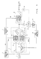
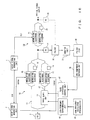
- Fig. 5 is a diagram describing a configuration of the optical transmitting apparatus of the first embodiment of the present invention. This optical transmitting apparatus generates and transmits a DQPSK optical signal in the following description.
- a clock signal generation unit 1 generates a clock signal.
- the frequency of the clock signal is, for example, a symbol frequency. In this case, if the bit rate of the transmitted data is 43Gbps, the symbol frequency is 21.5GHz.
- a drive signal generation unit 2 generates data signals DATA1 and DATA2 for generating a modulated optical signal.
- the data signals DATA1 and DATA2 can be obtained by encoding the transmission data using a DQPSK pre-coder.
- An optical source (LD) 3 is a semiconductor laser, for example, and generates an optical CW. The wavelength of the optical CW is not limited in particular; however, 1550nm band is used for example.
- a data modulator unit 10 generates a DQPSK optical signal by modulating the optical CW using the data signals DATA1 and DATA2, as explained with reference to Fig. 3 .
- the data modulator unit 10 is an interferometer, and comprises an optical splitter for splitting the input optical CW, a pair of optical waveguides (an arm 11 and an arm 12) for propagating a pair of optical signals obtained by the optical splitter, and an optical coupler for coupling the optical signals propagated via the pair of the optical waveguides.
- phase modulators 13 and 14 are configured respectively. Both phase modulators 13 and 14 are for example Mach-Zehnder interferometers.
- the phase modulator 13 comprises a modulating electrode 15 to which the data signal DATA1 is provided, and the phase modulator 14 comprises a modulating electrode 17 to which the data signal DATA2 is provided.
- the phase modulators 13 and 14 modulate the optical CW using the data signals DATA1 and DATA2, respectively.
- Each of the phase modulators 13 and 14 comprises bias input units 16 and 18, respectively, to which a bias signal for compensating for DC drift is provided.
- a phase shift unit 19 gives a prescribed phase difference to a pair of optical signals propagated via the arms 11 and 12.
- the "prescribed phase difference" is, in the DQPSK, "n ⁇ /2 (where n is an arbitrary odd number)".
- the phase shift unit 19, for example, by changing an optical length of an optical waveguide constituting the arm 12, adjusts the phase of an optical signal transmitted in the optical waveguide.
- the phase shift unit 19, for example, is a heater for adjusting the optical length by changing the temperature in a part of the optical waveguide constituting the arm 12.
- An intensity modulator 20 is a Mach-Zehnder interferometer, for example, and comprises a modulating electrode 21 to which a clock signal is provided, and a bias input unit 22 to which a bias signal for compensating for a DC drift is provided.
- the intensity modulator 20 modulates a DQPSK optical signal generated by the data modulator unit 10 by an intensity modulation (optical RZ modulation), using the clock signal. By so doing, an RZ-DQPSK signal is generated.
- the RZ-DQPSK signal can be obtained by lowering optical power of the DPSK signal in a period equivalent to the symbol rate.
- a polarization maintaining optical fiber may be used for the connections between the optical source 3 and the data modulator unit 10, and between the data modulator unit 10 and the intensity modulator 20. It is desirable that a configuration using a polarization maintaining optical fiber is applied, basically, to all embodiments.
- a Photodetector (PD) 31 converts a part of the DQPSK optical signal output from the data modulator unit 10 into an electrical signal.
- the photodetector 31 is a high-speed photodiode (or a phototransistor etc.), of which the cut-off frequency is a symbol frequency or higher, for example.
- a filter 32 extracts prescribed frequency components from the output signal of the photodetector 31.
- the filter 32 is a filter, which passes at least a part of contiguous frequency components except for an N-fold frequency of the symbol frequency (where N is an integer including 1), and is a band-pass filter or a low-pass filter with the cut-off frequency lower than the symbol frequency.
- a monitor unit 33 detects the power of the output signal of the filter 32.
- a phase difference control unit 34 adjusts the amount of phase shift in the phase shift unit 19 based on the detection result of the monitor unit 33 (i.e. a signal indicating the power of the output signal of the filter 32).
- the phase shift unit 19 comprises a heater for changing the temperature of the optical waveguide
- the phase difference control unit 34 adjusts electrical current to be provided to the heater based on the detection result of the monitor unit 33.
- a photodetector 35 instead of a photodetector 31, for converting a part of the RZ-DQPSK optical signal output from the intensity modulator 20 into an electrical signal.
- the filter 32 extracts prescribed frequency components from the output signal of the photodetector 35.
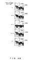
- Fig. 6A is a simulation result of the relation between the amount of phase shift in the phase shift unit 19 and the waveform of the output signal of the intensity modulator 20.
- Fig. 6B is a simulation result of the relation between the amount of phase shift in the phase shift 19 and the spectrum of the output signal of the intensity modulator 20.
- the output signal of the intensity modulator 20 has a waveform in which an approximately fixed optical power appears in a symbol period. Therefore, in such a case, the output signal of the intensity modulator 20 has large spectra at a symbol frequency component (21.5 GHz in this case) and at its harmonic components (43 GHz etc.), and small spectra at other frequency components.
- the output signal of the intensitymodulator 20 has a waveform in which different optical power appears in a random period.
- the spectrum of the output signal of the intensity modulator 20 comprises various frequencies, as shown in Fig. 6B .
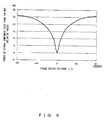
- Fig. 7 is a diagram showing a relation between the power of the output signal of the filter 32 and the amount of phase shift when the output signal of the intensity modulator 20 is monitored.
- the output signal of the photodetector 35 is provided to the filter 32.
- the filter 32 is a low-pass filter with the cut-off frequency of 100 MHz, and the cut-off frequency of the photodetector 35 is higher than that of the filter 32.
- Fig. 7 indicates a relative value on the basis of the minimum power of the output signal of the filter 32.
- the X-axis of Fig. 7 indicates deviation from " ⁇ /2".
- the power detected by the monitor unit 33 reaches its minimum as shown in Fig. 7 .
- the frequency components other than the symbol frequency component and its harmonic components become large. In other words, a high proportion of various frequency components (particularly components with lower frequency than the symbol frequency) are comprised. Therefore, in this case, the power detected by the monitor unit 33 is higher than the power when the amount of phase shift is " ⁇ /2", as shown in Fig. 7 . At that time, the power is determined in accordance with the amount of deviation from " ⁇ /2".
- the power of the output signal of the filter 32 reaches its minimum when the amount of phase shift in the phase shift unit 19 is adjusted to exactly " ⁇ /2". Therefore, by performing a feedback control so that the power of the output signal of the filter 32 reaches the minimum, the amount of phase shift in the phase shift unit 19 converges on " ⁇ /2".
- Fig. 8A is a simulation result of the relation between the amount of phase shift in the phase shift unit 19 and the waveform of the output signal of the data modulator unit 10.
- Fig. 8B is a simulation result of the relation between the amount of phase shift in the phase shift unit 19 and the spectrum of the output signal of the data modulator unit 10.
- Fig. 9 is a diagram showing the relation between the power of the output signal of the filter 32 and the amount of phase shift when the output signal of the data modulator unit 10 is monitored.
- the output signal of the photodetector 31 is provided to the filter 32.
- the filter 32 is a low-pass filter with cut-off frequency of 100 MHz, and the cut-off frequency of the photodetector 31 is higher than that of the filter 32.
- the power change with respect to the amount of phase shift shows larger and more rapid in the configuration for monitoring the output signal of the intensity modulator 20 than the configuration for monitoring the output signal of the data modulator unit 10.
- the power change detected by the monitor unit 33 when the amount of phase shift deviated by 5 degrees from " ⁇ /2", is less than 10 dB in the configuration for monitoring the output signal of the data modulator unit 10; however it is more than 20 dB in the configuration for monitoring the output signal of the intensity modulator 20.
- the configuration for monitoring the output signal of the intensity modulator 20 is advantageous to accurately adjust the amount of phase shift in the phase shift unit 19.
- the power of the optical signal input to the photodetector 35 drops by the loss. Therefore, which of the photodetectors 31 or 35 is used should be determined in consideration of the optical power at each point in the actual apparatus.
- Fig. 10 is a variation of the optical transmitting apparatus of the first embodiment.
- the optical transmitting apparatus shown in Fig. 10 can be realized by replacing the photodetector 31 and the filter 32 comprised in the optical transmitting apparatus shown in Fig. 5 with a photodetector 36 (or by replacing the photodetector 35 and the filter 32 with a photodetector 37) .
- the photodetectors 36 and 37 are medium-speed photodiodes, for example, and comprises a cut-off frequency lower than the symbol frequency. By so doing, the same function as the optical transmitting apparatus shown in Fig. 5 can be realized.
- the cut-off frequency of the photodetectors 36 and 37 is 100 MHz, characteristics in Fig. 6A-Fig. 9 can be obtained.
- Fig. 11 is a diagram showing a first configuration of an optical transmitting apparatus of the second embodiment of the present invention.
- the amount of phase shift is adjusted using a low-frequency signal.
- Numerical references shared in Fig. 5 and Fig. 11 indicate the same elements.
- a low-frequency oscillator 41 generates a low-frequency signal with several kHz through several MHz.
- the frequency of the low-frequency signal is referred to as "f 0 ".
- the low-frequency signal is a sinusoidal signal or rectangular wave signal, for example, and its amplitude is so small as not to give adverse effect on optical signals to be transmitted.
- the low-frequency signal is fed to the phase shift unit 19 via a low-frequency superimposing unit 42. For that reason, the amount of phase shift in the phase shift unit 19 changes (or dithers) on a periodic basis in accordance with the voltage of the low-frequency signal.
- a low-frequency detector unit 43 performs synchronous detection of the f 0 component signal in the output signal of the monitor unit 33 using the low-frequency signal generated by the low-frequency oscillator 41.
- the low-frequency detector unit 43 may comprise a low-pass filter or a band-pass filter, which passes the frequency f 0 .
- the operation and the configuration of the circuit performing the synchronous detection are heretofore known, and thus explanations of those are omitted.
- a phase difference control unit 44 adjusts the amount of phase shift of the phase shift unit 19 based on the detection result by the low-frequency detector unit 43 (the phase or the amplitude of the f 0 component signal, for example).
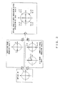
- Fig. 12A-Fig. 12C are diagrams explaining the principle of an adjustment method of the amount of phase shift in the second embodiment.
- the power detected by the monitor unit 33, as shown in Fig. 12A depends on the amount of phase shift in the phase shift unit 19, and becomes minimum when the amount of phase shift is " ⁇ /2".
- the relation shown in Fig. 12A is the same as in Fig. 7 .
- a low-frequency signal is provided to the phase shift unit 19. Then, the amount of phase shift of the phase shift unit 19 changes at the frequency f 0 . At that time, the amount of phase shift is " ⁇ /2", or is close to " ⁇ /2", the amount of phase shift, when the low-frequency signal is provided, periodically changes around a point where the power of the frequency component passing through the filter 32 becomes minimum. For example, within one period of time of the low-frequency signal (time t1-t5) the power of the frequency component passing through the filter 32 changes in the following manner.
- the time t1 approximately +30 dB (relative value)
- the time t2 zero (relative value)
- the time t3 approximately +30 dB (relative value)
- the time t4 zero (relative value)
- the time t5 approximately +30 dB (relative value). That is, in this case, the power of the frequency component passing through the filter 32 periodically changes with a frequency of 2f 0 as shown in Fig. 12B . Therefore, the output signal of the monitor unit 33 comprises the 2f 0 component.
- the amount of phase shift when a low-frequency signal is provided, periodically changes in a region away from a point where the power of the frequency component passing through the filter 32 has a minimum value.
- the power of the frequency component passing through the filter 32 changes in the following manner.
- the time t4 approximately +39 dB (relative value)
- the time t5 approximately +36 dB (relative value). That is, in this case the output signal of the monitor unit 33 comprises the f 0 component as shown in Fig. 12C ; however, does not comprise the 2f 0 component.
- the phase difference control unit 44 can determine whether the amount of phase shift by the phase shift unit 19 should be increased or decreased (i.e. whether to rotate in the positive side or in the negative side) , based on the phase of the f 0 component signal detected by the low-frequency detector unit 43.
- Fig. 13 and Fig. 14 are diagrams describing a relation between the detected f 0 component and the phase deviation.
- Fig. 13 shows the f 0 component when the RZ-DQPSK optical signal is monitored using the photodetector 35
- Fig. 14 shows the f 0 component when the DQPSK optical signal is monitored using the photodetector 31.
- the change in “the power of the f 0 component detected by the low-frequency detector unit 43" with respect to “the deviation of the amount of phase shift” is larger when the RZ-DQPSK optical signal output from the intensity modulator 20 is monitored, compared with the change when the DQPSK optical signal output from the data modulator unit 10 is monitored. Consequently, the signal amplitude obtained by the synchronous detection is larger in the configuration using the photodetector 35.
- Fig. 15 is a diagram showing a second configuration of the optical transmitting apparatus of the second embodiment.
- the optical transmitting apparatus shown in Fig. 15 is realized by replacing the photodetector 31 and the filter 32 comprised in the optical transmitting apparatus shown in Fig. 11 with the photodetector 36 (or by replacing the photodetector 35 and the filter 32 with the photodetector 37).
- the photodetectors 36 and 37 comprise a cut-off frequency lower than the symbol frequency, as explained with reference to Fig. 10 . By so doing, the same function as in the optical transmitting apparatus shown in Fig. 11 can be realized.
- Fig. 16 is a diagram showing a third configuration of the optical transmitting apparatus of the second embodiment.
- the amount of phase shift is adjusted using the frequency component 2f 0 (a frequency twice as high as that of the low-frequency signal generated by the low-frequency oscillator 41).
- a filter 45 is a band-pass filter, which passes the frequency component 2f 0 .
- a 2f 0 component detector unit 46 detects the amplitude of the output signal of the filter 45. In other words, the 2f 0 detector unit 46 detects the amplitude of the 2f 0 component.
- a phase difference control unit 47 adjusts the amount of phase shift in the phase shift unit 19 so that the amplitude of the 2f 0 component detected by the 2f 0 component detector unit 46 becomes maximum. As explained with reference to Fig. 12A-Fig. 12C , the amplitude of the 2f 0 component becomes maximum when the amount of phase shift in the phase shift unit 19 is " ⁇ /2".
- Fig. 17 is a diagram showing a fourth configuration of the optical transmitting apparatus of the second embodiment.
- the clock signal generation unit 1 and the drive signal generation unit 2 are omitted.
- a control unit 104 is equivalent to the monitor unit 33, the low-frequency detector unit 43 and the phase difference control unit 44 shown in Fig. 11 .
- the control unit 104 is equivalent to the filter 45, the 2f 0 component detector unit 46 and the phase difference control unit 47 shown in Fig. 16 .
- electrodes 101 and 102 are configured in the later stage of the phase modulators 13 and 14, respectively.
- a phase shifter 103 generates a pair of low-frequency signal (f 0 ( ⁇ ), f 0 ( ⁇ -n ⁇ /2)) with a phase difference n ⁇ /2 (where n is a number except for 0 and natural numbers, which are integral multiples of 4) based on the low-frequency signal generated by the low-frequency oscillator 41.
- One of the low-frequency signals f 0 ( ⁇ ) is provided to the electrode 101, and the other low-frequency signal f 0 ( ⁇ -n ⁇ /2) is provided to the electrode 102.
- the low-frequency signal f 0 ( ⁇ ) is superimposed on the modulated optical signal output from the phase modulator 13, and the low-frequency signal f 0 ( ⁇ -n ⁇ /2) is superimposed on the modulated optical signal output from the phase modulator 14.
- the low-frequency signal is provided to the phase shift unit 19.
- a pair of the low-frequency signals is provided to the electrodes 101 and 102.
- the amount of phase shift can be adjusted by the same operation as in the first and the third configurations.
- Fig. 18 is a diagram showing a fifth configuration of the optical transmitting apparatus of the second embodiment.
- the amount of phase shift is adjusted using both of the frequency component f 0 and the frequency component 2f 0 .
- a low-speed photodetector 111 converts the DQPSK optical signal output from the data modulator unit 10 into an electrical signal.
- the low-frequency signal f 0 has been superimposed on the DQPSK optical signal.
- the low-speed photodetector 111 comprises a band (or response speed), which enables detection of the frequency twice as high as the frequency of the low-frequency signal generated by the low-frequency oscillator 41 (for example, several kHz through several MHz). It is also possible to use a low-speed photodetector 115 for converting the RZ-DQPSK optical signal output from the intensity modulator 20 into an electrical signal instead of using the low-speed photodetector 111.
- a filter 112 is a band-pass filter, which passes the frequency component f 0 .
- a phase comparator 113 performs synchronous detection for comparing the phase ⁇ 1 of the low-frequency signal generated by the low-frequency oscillator 41 with the phase ⁇ 2 of the low-frequency signal output from the filter 112, and detects the sign (or polarity) of the phase of the output signal from the filter 112. At that time, it is possible that, if the phase ⁇ 1 and the phase ⁇ 2 have the same sign, for example, the phase comparator 113 outputs a sign signal indicating "positive", and if signs of the phase ⁇ 1 and the phase ⁇ 2 opposite to each other, the phase comparator 113 outputs a sign signal indicating "negative".
- the filter 45 and the 2f 0 component detector unit 46 are the same as explained with reference to Fig. 16 , and detect the amplitude of the 2f 0 component.
- a control unit 114 adjusts the amount of phase shift in the phase shift unit 19 based on the output of the phase comparator 113 and the 2f 0 component detector unit 46. Practically, the control unit 114, for examples, determines whether the DC bias should be increased or decreased based on the sign detected by the phase comparator 113 when adjusting the amount of phase shift so that the amplitude of the 2f 0 component detected by the 2f 0 component detector unit 46 becomes maximum.
- Fig. 19 is a diagram showing sixth and seventh configurations of the optical transmitting apparatus of the second embodiment.
- the sixth and the seventh configurations in addition to the adjustment of the amount of phase shift in the phase shift unit 19, compensation for the DC drift in the phase modulators 13 and 14 (deviation in the operating point of a Mach-Zehnder type modulator) and compensation for the DC drift in the intensity modulator 20 are performed.
- a low-frequency signal is superimposed on an optical signal as in the first through the fifth configurations.
- a monitor unit 120 monitors the low-freauency signal included in the DQPSK optical signal output from the data modulator unit 10 and/or the RZ-DQPSK optical signal output from the intensity modulator 20.
- a phase shift control unit 130 based on the monitoring result of the monitor unit 120, adjusts the amount of phase shift in the phase shift unit 19 using a control signal (1). The operation of the phase shift control unit 130 is the same as explained with reference to Fig. 11 through Fig. 18 .
- a 2V ⁇ -ABC (Automatic Bias Control) unit 140 based on the monitoring result by the monitor unit 120, generates control signals (2) and (3) for compensating for the DC drift in the phase modulators 13 and 14.
- V ⁇ -ABC unit 150 based on the monitoring result by the monitor unit 120, generates a control signal (4) for compensating for the DC drift in the intensity modulator 20.
- the operation of the V ⁇ -ABC is the heretofore know art.
- Fig. 20 is a diagram explaining the operation of the control system of the sixth configuration of the optical transmitting apparatus of the second embodiment.
- adjustment and compensation are performed by the time-division method.
- the monitor unit 120 performs a monitoring operation for adjusting the amount of the phase shift, a monitoring operation for compensating for the DC drift in the phase modulators 13 and 14, and a monitoring operation for compensating for the DC drift in the intensity modulator 20 by the time-division method.
- a switch control unit 121 sequentially switches the forwarding destinations (the phase shift control unit 130, 2V ⁇ -ABC units 141 and 142, and the V ⁇ -ABC unit 150) of the monitoring result by the monitor unit 120.
- the low-frequency signal f 0 is generated in the switch control unit 121, for example.
- the low-frequency signal f 0 may be superimposed on the control signal (1) and provided to the phase shift unit 19, for example, may be superimposed on the control signals (2) and (3) and provided to the phase modulators 3 and 4, respectively, and may be superimposed on the control signal (4) and provided to the intensity modulator 20.
- Fig. 21 through Fig. 23 are examples of implementation of the sixth configuration.
- a monitor unit 120a is a medium-speed photodetector comprising a band of several tens of MHz through several GHz, and detects a prescribed continuous frequency components lower than the symbol frequency.
- the monitor unit 120a is equivalent to a combination of the photodetector 31 and the filter 32, or the photodetector 36.
- the phase shift control unit 130 generates the control signal (1) based on the monitoring result by the monitor unit 120a. By so doing, the amount of phase shift in the phase shift unit 19 can be adjusted.
- a monitor unit 120b is a low-speed photodetector comprising a band of several kHz through several MHz, and detects the low-frequency signal f 0 .
- the switch control unit 121a sequentially switches the forwarding destinations of the monitoring result by the monitor unit 120b (2V ⁇ -ABC units 141 and 142, and the V ⁇ -ABC unit 150).
- the 2V ⁇ -ABC units 141 and 142, and the V ⁇ -ABC unit 150 based on the provided monitoring result, generate the control signals (2)-(4) by the time-division method.
- a switch control unit 121b sequentially switches the forwarding destinations of the monitoring result by the monitor unit 120a (the phase shift control unit 130, and the 2V ⁇ -ABC units 141 and 142).
- the phase shift control unit 130, and the 2V ⁇ -ABC units 141 and 142 based on the provided monitoring result, generate the control signals (1)-(3) by the time-division method.
- the V ⁇ -ABC unit 150 based on the monitoring result by the monitor unit 120b, generates the control signal (4).
- a switch control unit 121c sequentially switches the forwarding destinations of the monitoring result by the monitor unit 120a (the phase shift control unit 130, the 2V ⁇ -ABC units 141 and 142, and the V ⁇ -ABC unit 150).
- the monitor unit 120a monitors the optical output of the intensity modulator 20.
- the phase shift control unit 130, the 2V ⁇ -ABC units 141 and 142, and the V ⁇ -ABC unit 150 based on the provided monitoring result, generate the control signals (1)-(4) by the time-division method.
- Fig. 24 is a diagram explaining the operation or the control system of the seventh configuration of the optical transmitting apparatus of the second embodiment.
- adjustment of the amount of phase shift and the DC drift is performed using a plurality of low-frequency signals with different frequencies.
- the amount of phase shift in the phase shift unit 19 is adjusted using the low-frequency signal with frequency f 0
- the DC drift of the phase modulator 13 is adjusted using the low-frequency signal with frequency f 1
- the DC drift of the phase modulator 14 is adjusted using the low-frequency signal with frequency f 2
- the DC drift of the intensity modulator 20 is adjusted using the low-frequency signal with frequency f 3 .
- All of the frequencies f 0 -f 3 are selected within a range from several kHz to several MHz.
- the low-frequency signal f 0 is superimposed on the control signal (1) and provided to the phase shift unit 19, the low-frequency signals f 1 and f 2 are superimposed on the control signals (2) and (3), respectively, and provided to the phase modulators 13 and 14, respectively, and the low-frequency signal f 3 is superimposed on the control signal (4) and provided to the intensity modulator 20.
- a monitor unit 161 monitors the frequency components f 0 -f 3 (or 2f 0 -2f 3 ) in parallel.
- a collective control unit 162 forwards each of the monitoring results obtained by the monitor unit 161 to the phase shift control unit 130, the 2V ⁇ -ABC units 141 and 142, and the V ⁇ -ABC unit 150. Then, the phase shift control unit 130, the 2V ⁇ -ABC units 141 and 142, and the V ⁇ -ABC unit 150, based on the provided monitoring result, generate the control signals (1)-(4). According to this configuration, adjustment of the amount of phase shift and compensation for the DC drift can be performed simultaneously.
- Fig. 25-Fig. 27 are examples of implementation of the seventh configuration.
- the phase shift control unit 130 based on the monitoring result by the monitor unit 120a, generates the control signal (1). By so doing, the amount of phase shift in phase shift unit 19 can be adjusted.
- the collective control unit 162a informs the 2V ⁇ -ABC units 141 and 142, and the V ⁇ -ABC uni t 150 of the monitoring result by the monitor unit 120b.
- the 2V ⁇ -ABC units 141 and 142, and the V ⁇ -ABC unit 150 based on the provided monitoring result, generate the control signals (2)-(4).
- the collective control unit 162b provides the monitoring result by the monitor unit 120a to the phase shift control unit 130 and the 2V ⁇ -ABC units 141 and 142.
- the phase shift control unit 130 and the 2V ⁇ -ABC units 141 and 142 based on the provided monitoring result, generate the control signals (1)-(3).
- the V ⁇ -ABC unit 150 based on the monitoring result by the monitor unit 120b, generates the control signal (4).
- the collective control unit 162c provides the monitoring result by the monitor unit 120a to the phase shift control unit 130, the 2V ⁇ -ABC units 141 and 142, and the V ⁇ -ABC unit 150.
- the monitor unit 120a monitors the optical output of the intensity modulator 20.
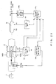
- Fig. 28 is a diagram showing a first configuration of the optical transmitting apparatus of the third embodiment of the present invention.
- Fig. 29 is a diagram showing a second configuration of the optical transmitting apparatus of the third embodiment of the present invention.
- the numerical references in common among Fig 5 , Fig. 28 and Fig. 29 indicate the same elements. Either of the photodetector 31 or the photodetector 35 can be used as a photodetector.
- a DC component removal element 51 is, for example, a condenser, and removes the DC component from the output signal of the filter 32.
- a mixer 52 squares the output signal of the DC component removal element 51.
- the mixer circuit 52 is not limited in particular; however, is realized by an analog multiplier circuit comprising a Gilbert cell, for example. In such a case, a squared signal is obtained by multiplying the output signal of the DC component removal element 51 by itself using the analog multiplier circuit.
- An integrator circuit 53 integrates the squared signal output from the mixer 52.
- An integration time is from several thousand to several tens of thousand times of the symbol time, for example.
- the integrator circuit 53 repeatedly executes the integration operation.
- a phase difference control unit 54 adjusts the amount of phase shift in the phase shift unit 19 based on the integration result obtained by the integrator circuit 53.
- the optical transmitting apparatus of the second configuration shown in Fig. 29 comprises a peak hold circuit 55 instead of the integrator circuit 53 shown in Fig. 28 .
- the peak hold circuit 55 detects a peak value of the squared signal output from the mixer 52.
- a sampling time is from several thousand to several tens of thousand times of the symbol time, for example.
- the peak hold circuit 55 repeatedly executes the sampling/hold operation.
- a phase difference control unit 56 adjusts the amount of phase shift in the phase shift unit 19 based on the peak value obtained by the peak hold circuit 55.
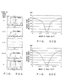
- Fig. 30A is a diagram showing a waveform of the output signal of the mixer 52 (i.e. the squared signal).
- Fig. 30B is a diagram showing the relation between the amount of phase shift and average power of the squared signal. The average power of the squared signal is equivalent to the integrated value obtained by the integrator circuit 53.
- the average power of the squared signal output from the mixer 52 is minimum when the amount of phase shift in the phase shift unit 19 is exactly " ⁇ /2"(i.e. when the deviation of the amount of phase shift in the phase shift unit 19 is zero). As the deviation from " ⁇ /2" becomes large, the average power of the squared signal becomes larger. Therefore, by periodically calculating an integrated value or an average value of the squared signal output from the mixer 52, and performing a feedback control so that the calculated value becomes minimum, the amount of phase shift in the phase shift unit 19 can be converged on " ⁇ /2".
- the amount of phase shift can be adjusted without configuring the DC component removal element 51.
- the mixer 52 squares the output signal of the filter 32.
- an integrated value or an average value of the squared signal depends on the amount of phase shift in the phase shift unit 19, and reaches minimum when the amount of phase shift is " ⁇ /2". Consequently, the amount of phase shift can be properly adjusted by the same feedback control.
- the squared signal is generated in a state that the DC component still remains, a change in the integrated value or the average value of the squared signal with respect to the change in the amount of phase shift becomes small. Therefore, the adjustment accuracy of the amount of phase shift can be higher in the configuration with the DC component removal element 51.
- the integrated value or the average value of the output signal of the filter 32 is a constant value regardless of the amount of phase shift.
- the integrated value or the average value of the output signal of the DC component removal element 51 is zero regardless of the amount of phase shift.
- Fig. 30C is a diagram showing the relation between the amount of phase shift and the peak power of the squared signal.
- the peak power of the squared signal is detected by the peak hold circuit 55 shown in Fig. 29 .
- the peak power of the squared signal output from the mixer 52 becomes minimum when the amount of phase shift in the phase shift unit 19 is exactly " ⁇ /2". As the deviation from " ⁇ /2" becomes large, the peak power of the squared signal becomes large. Consequently, by periodically calculating the peak power of the squared signal output from the mixer 52, and by performing a feedback control so that the calculated value becomes minimum, the amount of phase shift in the phase shift unit 19 can be converged on " ⁇ /2".
- the peak power of the squared signal depends on the amount of phase shift in the phase shift unit 19, and becomes minimum when the amount of phase shift is " ⁇ /2". In other words, in the optical transmitting apparatus shown in Fig. 29 , the amount of phase shift can be properly adjusted without the DC component removal element 51.
- the optical peak power of the RZ-DQPSK optical signal or the DQPSK optical signal is minimum when the amount of phase shift is " ⁇ /2". Therefore, if a detection system of the optical signal (a photodetector element and a peak hold circuit etc.) can keep up with the symbol rate, it is possible to adjust the amount of phase shift in accordance with the optical peak power of the RZ-DQPSK optical signal or the DQPSK optical signal.
- the phase shift unit 19 can be configured in the former stage of the phase modulator 13 or 14, or can be configured in the later stage of the phase modulator 13 or 14.
- the intensity modulator 20 can be configured in the later stage of the data modulator unit 10 or in the former stage of the data modulator unit 10.
- a part of the DQPSK optical signal output from the data modulator unit 10 is split and directed to the photodetector 31 (or the photodetector 36).
- a part of the RZ-DQPSK optical signal output from the intensity modulator 20 is split and directed to the photodetector 35 (or the photodetector 37).
- these optical signals are, for example, split by an optical splitter and are directed to the corresponding photodetector.
- the "splitting" of the optical signal in the present invention is not limited to a configuration using an optical splitter; however, a configuration, in which an emission leaked from a coupled part of the optical waveguide is directed to the photodetector, is also possible.
- a technique for monitoring optical leak of an MZ modulator is described in Japanese Patent Application Laid-open Publication No. H10-228006 .
- the output side waveguide of the data modulator unit 10 or the intensity modulator 20 is coupled with an X-coupler (intersecting waveguide), it is possible to direct a reverse phase optical signal to the photodetector as well as outputting the in-phase optical signal as a main signal.
- An. X-coupler optical modulator is described in Japanese Patent Application Laid-open Publication No. 2001-244896 , for example.
- the photodetectors (31, 35, 36 and 37) for detecting the DQPSK optical signal or the RZ-DQPSK optical signal may be incorporated in the modulators (the data modulator unit 10 or the intensity modulator 20), or may be configured outside of the modulators.
- the amount of phase shift in the phase shift unit 19 can be adjusted by, for example, changing the refractive index of the optical waveguide.
- the refractive index of the optical waveguide can be adjusted by, for example, arranging a thin-film heater etc. adjacent to the optical waveguide to change the temperature of the optical waveguide, or by arranging a piezoelectric element etc. for applying appropriate voltage to give stress to the waveguide, or for applying voltage to induce an electro-optic effect (Pockels effect).
- phase shift unit 19 is configured in one of the optical waveguides of the interferometer in the above embodiments, it can be configured in both of a pair of the waveguides. In such a case, by making the applied voltage and the temperature provided to the phase shift unit (the electrodes, the thin-film heater, piezoelectric elements and others) configured in a pair of waveguides asymmetrical, the relative phase difference can be provided.
- a 2V ⁇ -ABC unit is used instead of a V ⁇ -ABC unit 150 in Fig. 19 through Fig. 27 .
- the absolute-value circuit is a circuit for performing full-wave rectification of the signal output from the DC component removal circuit, and though it is not limited in particular, it is realized by, for example, a full-wave rectifier circuit in which a plurality of diodes are connected, or by a full-wave rectifier circuit formed by using an operational amplifier.
- DQPSK modulation is mainly explained; however, the control of the present invention is applicable to the QPSK modulation without any modification.
- the present invention is also applicable to 2 n PSK (n ⁇ 3) or QAM.
- multi-level data with four or more values should be used as a data signal input to the data modulation unit.
Description
- The present invention relates to an optical transmitting apparatus, and in particular, relates to optical transmitting apparatus for transmitting an optical signal using PSK modulation.
- Development of a practical implementation of an optical transmitting apparatus aiming to establish a high capacity and long distance optical transmission system has been awaited in recent years. Particularly, expectations for implementation of an optical transmitting apparatus, which employs an optical modulation technique adequate for high capacity and long-distance, to an actual system are growing high. In order to meet with expectations, optical transmission systems using phase shift keying such as DPSK (Differential Phase Shift Keying) and DQPSK (Differential Quadrature Phase Shift Keying) are envisioned.
-
Fig. 1 is a diagram showing a configuration of optical 1 transmitting apparatus, which is heretofore known, for transmitting a QPSK signal or a DQPSK signal. Inoptical transmitting apparatus 2000 shown inFig. 1 , an optical source (LD) 2001 generates an optical continuous wave (CW). Anoptical splitter 2002 splits the optical CW and guides toarms arms phase modulators phase modulators phase modulator 2005 performs phase modulation of the opticalCW using data 1, and thephase modulator 2006 performs phase modulation of the opticalCW using data 2. In DQPSK, thedata 1 anddata 2 are encoded by a DQPSK pre-coder. Anoptical coupler 2007 couples modulated signals obtained from thephase modulators phase shifter 2008 causes the phase difference of π/2 between an optical signal guided to theoptical coupler 2007 via thearm 2003 and an optical signal guided to theoptical coupler 2007 via thearm 2004. By the above configuration, a QPSK optical signal or a DQPSK optical signal is generated. Details of the configuration and the operation of DQPSK optical transmitting apparatus are described, for example, in Patent Document 1 (Japanese Patent Application Laid-open Publication No.2004-516743 WO2002/051041 orUS2004/0081470 )). - As a related art, Patent Document 2 (Japanese Patent Application Laid-open Publication No.
2004-318052 - As other related arts, Patent documents 3 (Japanese Patent Application Laid-open Publication No.
H03-251815 H09-261207 - In the optical transmitting apparatus shown in
Fig. 1 , it is necessary for the amount of phase shift provided by the phase shifter 2008 ("π/2" in the QPSK and the DQPSK) to be set accurately to attain favorable reception quality. However, the amount of phase shift may sometimes deviate from a prescribed value due to thermal change and aged degradation etc. - Nevertheless, in the conventional technologies, a configuration for adjusting the amount of phase shift of the phase shifter in response to thermal change or aged degradation etc. has not been suggested.
-
WO-A1-03/049333 -
US-A1-2005/0088659 discloses feedback control of an interferometer in which a portion of a data signal is split and rectified and the signal intensity is detected with slow speed electronics for improving the control of a delay line interferometer (DLI) used in optical data transmission. A control signal is generated and fed back to the DLI based on the detected signal intensity. Further, a device is provided with a DLI, a first and second optoelectronic component, and a differential amplifier. - It is an object of the present invention to provide a configuration, which allows appropriate adjustment of the amount of phase shift in an optical transmitting apparatus comprising a phase modulator.
- The present invention provides an optical transmitting apparatus as set out in
Claim 1. -
-
Fig. 1 is a diagram showing a configuration of conventional optical transmitting apparatus for transmitting a QPSK signal or a DQPSK signal; -
Fig. 2 is a diagram showing a configuration of an optical communication system relating to the embodiments of the present invention; -
Fig. 3 is a diagram explaining the principle of the DQPSK modulation; -
Fig. 4 is a diagram explaining deterioration of communication quality in the DQPSK modulation; -
Fig. 5 is a diagram describing a configuration of the optical transmitting apparatus of the first embodiment of the present invention; -
Fig. 6A andFig. 6B are simulation results of the waveform and the spectrum of the output signal of the intensity modulator; -
Fig. 7 is a diagram showing a relation between the filter output power and the amount of phase shift when the output signal of the intensity modulator is monitored; -
Fig. 8A andFig. 8B are simulation results of the waveform and the spectrum of the output signal of the data modulator unit; -
Fig. 9 is a diagram showing the relation between the filter output power and the amount of phase shift when the output signal of the data modulator unit is monitored; -
Fig. 10 is a variation of the optical transmitting apparatus of the first embodiment; -
Fig. 11 is a diagram showing a first configuration of an optical transmitting apparatus of the second embodiment of the present invention; -
Fig. 12A-Fig. 12C are diagrams explaining the principle of an adjustment method of the amount of phase shift in the second embodiment; -
Fig. 13 is a diagram describing a relation between the f0 component and the phase deviation when the output signal of the intensity modulator is monitored; -
Fig. 14 is a diagram describing a relation between the f0 component and the phase deviation when the output signal of the data modulator unit is monitored; -
Fig. 15 through Fig. 18 are diagrams showing second through fifth configurations of the optical transmitting apparatus of the second embodiment, respectively; -
Fig. 19 is a diagram showing sixth and seventh configurations of the optical transmitting apparatus of the second embodiment; -
Fig. 20 is a diagram explaining the operation of the control system of the sixth configuration of the optical transmitting apparatus of the second embodiment; -
Fig. 21 through Fig. 23 are first through third example implementations of the sixth configuration, respectively; -
Fig. 24 is a diagram explaining the operation of the control system of the seventh configuration of the optical transmitting apparatus of the second embodiment; -
Fig. 25 through Fig. 27 are first through third example implementations of the seventh configuration, respectively; -
Fig. 28 andFig. 29 are diagrams showing first and second configurations of the optical transmitting apparatus of the third embodiment of the present invention, respectively; -
Fig. 30A is a diagram showing a waveform of the squared signal; -
Fig. 30B is a diagram showing the relation between the amount of phase shift and average power of the squared signal; and -
Fig. 30C is a diagram showing the relation between the amount of phase shift and the peak power of the squared signal. - In the following description, the preferred embodiments of the present invention are set forth with reference to the drawings.
-
Fig. 2 is a diagram showing a configuration of an optical communication system relating to the preferred embodiments of the present invention. Anoptical communication system 1000 shown inFig. 2 comprises anoptical transmitting apparatus 1010, anoptical receiving apparatus 1020, and a transmissionoptical fiber 1030 for connecting between them. Theoptical transmitting apparatus 1010 comprises adata generation unit 1011 and amodulator 1012. Thedata generation unit 1011 generates data to be transmitted. Themodulator 1012 generates a modulated optical signal using the data generated by thedata generation unit 1011. In this case, the modulation method is not limited in particular but is the DQPSK, for example. Theoptical receiving apparatus 1020 obtains data by demodulating an optical signal transmitted via the transmissionoptical fiber 1030. An optical amplifier or an optical repeater can be provided on the transmissionoptical fiber 1030. -
Fig. 3 is a diagram explaining the principle of the DQPSK (or QPSK) modulation. In the DQPSK modulation, two-bit data (data 1, data 2) is transmitted as one symbol. Here, each symbol is assigned with a phase corresponding to a combination of the data (data 1, data2). In the example shown inFig. 3 , "π/4" is assigned to the symbol (0, 0) , "3π/4" is assigned to the symbol (1,0), "5π/4" is assigned to the symbol (1,1), and "7π/4" is assigned to the symbol (0,1). Therefore, the optical receiving apparatus can recover data by detecting the phase of the received signal. - In order to achieve the above phase modulation, an optical CW (Continuous Wave) is split into two, and one of the split light is phase-modulated by the
data 1 and the other split light is phase-modulated by thedata 2. Then, the phase assigned to thedata 2 is shifted by "π/2" with respect to the phase assigned to thedata 1. In other words, a device to generate π/2-phase shift is required in the DQPSK modulation. -
Fig. 4 is a diagram explaining deterioration of communication quality in the DQPSK modulation. An optical transmitting apparatus employing the DQPSK modulation, as described above, comprises a device for generating π/2-phase shift. However, when the amount of phase shift deviates from π/2 due to thermal change or aged degradation etc., the positions of each symbol on a phase plane also deviate, as shown inFig. 4 , and the possibility of erroneous data recognition increases in an optical receiving apparatus. Therefore, in order to improve the communication quality of the DQPSK modulation system, it is important to maintain high accuracy of the π/2-phase shift device. -
Fig. 5 is a diagram describing a configuration of the optical transmitting apparatus of the first embodiment of the present invention. This optical transmitting apparatus generates and transmits a DQPSK optical signal in the following description. - In
Fig. 5 , a clocksignal generation unit 1 generates a clock signal. The frequency of the clock signal is, for example, a symbol frequency. In this case, if the bit rate of the transmitted data is 43Gbps, the symbol frequency is 21.5GHz. A drivesignal generation unit 2 generates data signals DATA1 and DATA2 for generating a modulated optical signal. Here, the data signals DATA1 and DATA2 can be obtained by encoding the transmission data using a DQPSK pre-coder. An optical source (LD) 3 is a semiconductor laser, for example, and generates an optical CW. The wavelength of the optical CW is not limited in particular; however, 1550nm band is used for example. - A
data modulator unit 10 generates a DQPSK optical signal by modulating the optical CW using the data signals DATA1 and DATA2, as explained with reference toFig. 3 . Thedata modulator unit 10 is an interferometer, and comprises an optical splitter for splitting the input optical CW, a pair of optical waveguides (anarm 11 and an arm 12) for propagating a pair of optical signals obtained by the optical splitter, and an optical coupler for coupling the optical signals propagated via the pair of the optical waveguides. On thearm 11 and thearm 12,phase modulators phase modulators phase modulator 13 comprises a modulatingelectrode 15 to which the data signal DATA1 is provided, and thephase modulator 14 comprises a modulatingelectrode 17 to which the data signal DATA2 is provided. Thephase modulators phase modulators bias input units - A
phase shift unit 19 gives a prescribed phase difference to a pair of optical signals propagated via thearms phase shift unit 19, for example, by changing an optical length of an optical waveguide constituting thearm 12, adjusts the phase of an optical signal transmitted in the optical waveguide. Thephase shift unit 19, for example, is a heater for adjusting the optical length by changing the temperature in a part of the optical waveguide constituting thearm 12. - An
intensity modulator 20 is a Mach-Zehnder interferometer, for example, and comprises a modulatingelectrode 21 to which a clock signal is provided, and abias input unit 22 to which a bias signal for compensating for a DC drift is provided. Theintensity modulator 20 modulates a DQPSK optical signal generated by thedata modulator unit 10 by an intensity modulation (optical RZ modulation), using the clock signal. By so doing, an RZ-DQPSK signal is generated. The RZ-DQPSK signal can be obtained by lowering optical power of the DPSK signal in a period equivalent to the symbol rate. - When an LN (LiNbO3) modulator is used as the
data modulator unit 10 and theintensity modulator 20, because the LN modulator has a polarization dependency, a polarization maintaining optical fiber may be used for the connections between theoptical source 3 and thedata modulator unit 10, and between thedata modulator unit 10 and theintensity modulator 20. It is desirable that a configuration using a polarization maintaining optical fiber is applied, basically, to all embodiments. - A Photodetector (PD) 31 converts a part of the DQPSK optical signal output from the
data modulator unit 10 into an electrical signal. Thephotodetector 31 is a high-speed photodiode (or a phototransistor etc.), of which the cut-off frequency is a symbol frequency or higher, for example. Afilter 32 extracts prescribed frequency components from the output signal of thephotodetector 31. Specifically, thefilter 32 is a filter, which passes at least a part of contiguous frequency components except for an N-fold frequency of the symbol frequency (where N is an integer including 1), and is a band-pass filter or a low-pass filter with the cut-off frequency lower than the symbol frequency. Amonitor unit 33 detects the power of the output signal of thefilter 32. - A phase
difference control unit 34 adjusts the amount of phase shift in thephase shift unit 19 based on the detection result of the monitor unit 33 (i.e. a signal indicating the power of the output signal of the filter 32). When thephase shift unit 19 comprises a heater for changing the temperature of the optical waveguide, the phasedifference control unit 34 adjusts electrical current to be provided to the heater based on the detection result of themonitor unit 33. In the above configuration, it is possible to set aphotodetector 35, instead of aphotodetector 31, for converting a part of the RZ-DQPSK optical signal output from theintensity modulator 20 into an electrical signal. In such a case, thefilter 32 extracts prescribed frequency components from the output signal of thephotodetector 35. -
Fig. 6A is a simulation result of the relation between the amount of phase shift in thephase shift unit 19 and the waveform of the output signal of theintensity modulator 20.Fig. 6B is a simulation result of the relation between the amount of phase shift in thephase shift 19 and the spectrum of the output signal of theintensity modulator 20. - As shown in
Fig. 6A , if the amount of phase shift in thephase shift unit 19 is exactly "π/2", the output signal of theintensity modulator 20 has a waveform in which an approximately fixed optical power appears in a symbol period. Therefore, in such a case, the output signal of theintensity modulator 20 has large spectra at a symbol frequency component (21.5 GHz in this case) and at its harmonic components (43 GHz etc.), and small spectra at other frequency components. On the other hand, when the amount of phase shift in thephase shift unit 19 deviates from "π/2", as shown inFig. 6A , the output signal of theintensitymodulator 20 has a waveform in which different optical power appears in a random period. Hence, in such a case, the spectrum of the output signal of theintensity modulator 20 comprises various frequencies, as shown inFig. 6B . -
Fig. 7 is a diagram showing a relation between the power of the output signal of thefilter 32 and the amount of phase shift when the output signal of theintensity modulator 20 is monitored. Here, the output signal of thephotodetector 35 is provided to thefilter 32. Thefilter 32 is a low-pass filter with the cut-off frequency of 100 MHz, and the cut-off frequency of thephotodetector 35 is higher than that of thefilter 32. In addition,Fig. 7 indicates a relative value on the basis of the minimum power of the output signal of thefilter 32. The X-axis ofFig. 7 indicates deviation from "π/2". - When the amount of phase shift in the
phase shift unit 19 is exactly "π/2", as stated above, the frequency components other than the symbol frequency component and its harmonic components are small. For that reason, the frequency component other than in such a case, the power detected by themonitor unit 33 reaches its minimum as shown inFig. 7 . On the other hand, when the amount of phase shift deviates from "π/2", the frequency components other than the symbol frequency component and its harmonic components become large. In other words, a high proportion of various frequency components (particularly components with lower frequency than the symbol frequency) are comprised. Therefore, in this case, the power detected by themonitor unit 33 is higher than the power when the amount of phase shift is "π/2", as shown inFig. 7 . At that time, the power is determined in accordance with the amount of deviation from "π/2". - As described above, the power of the output signal of the
filter 32 reaches its minimum when the amount of phase shift in thephase shift unit 19 is adjusted to exactly "π/2". Therefore, by performing a feedback control so that the power of the output signal of thefilter 32 reaches the minimum, the amount of phase shift in thephase shift unit 19 converges on "π/2". -
Fig. 8A is a simulation result of the relation between the amount of phase shift in thephase shift unit 19 and the waveform of the output signal of thedata modulator unit 10.Fig. 8B is a simulation result of the relation between the amount of phase shift in thephase shift unit 19 and the spectrum of the output signal of thedata modulator unit 10. Additionally,Fig. 9 is a diagram showing the relation between the power of the output signal of thefilter 32 and the amount of phase shift when the output signal of thedata modulator unit 10 is monitored. In other words, the output signal of thephotodetector 31 is provided to thefilter 32. Like the above example, thefilter 32 is a low-pass filter with cut-off frequency of 100 MHz, and the cut-off frequency of thephotodetector 31 is higher than that of thefilter 32. - As shown in
Fig. 8B andFig. 9 , even when the output signal of thedata modulator unit 10 is monitored, like the case when the output signal of theintensity modulator 20 is monitored, the frequency components other than the symbol frequency component and its harmonic components become minimum when the amount of phase shift in thephase shift unit 19 is "π/2". Therefore, in this case also, by performing a feedback control so that the power of the output signal of thefilter 32 reaches minimum, the amount of phase shift in thephase shift unit 19 converges on "π/2". - As it is clear from the comparison between
Fig. 7 andFig. 9 , the power change with respect to the amount of phase shift shows larger and more rapid in the configuration for monitoring the output signal of theintensity modulator 20 than the configuration for monitoring the output signal of thedata modulator unit 10. For example, the power change detected by themonitor unit 33, when the amount of phase shift deviated by 5 degrees from "π/2", is less than 10 dB in the configuration for monitoring the output signal of thedata modulator unit 10; however it is more than 20 dB in the configuration for monitoring the output signal of theintensity modulator 20. For that reason, the configuration for monitoring the output signal of theintensity modulator 20 is advantageous to accurately adjust the amount of phase shift in thephase shift unit 19. However, because a loss is caused in theintensity modulator 20, the power of the optical signal input to thephotodetector 35 drops by the loss. Therefore, which of thephotodetectors -
Fig. 10 is a variation of the optical transmitting apparatus of the first embodiment. The optical transmitting apparatus shown inFig. 10 can be realized by replacing thephotodetector 31 and thefilter 32 comprised in the optical transmitting apparatus shown inFig. 5 with a photodetector 36 (or by replacing thephotodetector 35 and thefilter 32 with a photodetector 37) . In this example, thephotodetectors Fig. 5 can be realized. In other words, when the cut-off frequency of thephotodetectors Fig. 6A-Fig. 9 can be obtained. -
Fig. 11 is a diagram showing a first configuration of an optical transmitting apparatus of the second embodiment of the present invention. In the optical transmitting apparatus of the second embodiment, the amount of phase shift is adjusted using a low-frequency signal. Numerical references shared inFig. 5 andFig. 11 indicate the same elements. - A low-
frequency oscillator 41 generates a low-frequency signal with several kHz through several MHz. In the following description, the frequency of the low-frequency signal is referred to as "f0". The low-frequency signal is a sinusoidal signal or rectangular wave signal, for example, and its amplitude is so small as not to give adverse effect on optical signals to be transmitted. The low-frequency signal is fed to thephase shift unit 19 via a low-frequency superimposing unit 42. For that reason, the amount of phase shift in thephase shift unit 19 changes (or dithers) on a periodic basis in accordance with the voltage of the low-frequency signal. - A low-
frequency detector unit 43 performs synchronous detection of the f0 component signal in the output signal of themonitor unit 33 using the low-frequency signal generated by the low-frequency oscillator 41. Here, the low-frequency detector unit 43 may comprise a low-pass filter or a band-pass filter, which passes the frequency f0. The operation and the configuration of the circuit performing the synchronous detection are heretofore known, and thus explanations of those are omitted. A phasedifference control unit 44 adjusts the amount of phase shift of thephase shift unit 19 based on the detection result by the low-frequency detector unit 43 (the phase or the amplitude of the f0 component signal, for example). -
Fig. 12A-Fig. 12C are diagrams explaining the principle of an adjustment method of the amount of phase shift in the second embodiment. The power detected by themonitor unit 33, as shown inFig. 12A , depends on the amount of phase shift in thephase shift unit 19, and becomes minimum when the amount of phase shift is "π/2". The relation shown inFig. 12A is the same as inFig. 7 . - A low-frequency signal is provided to the
phase shift unit 19. Then, the amount of phase shift of thephase shift unit 19 changes at the frequency f0. At that time, the amount of phase shift is "π/2", or is close to "π/2", the amount of phase shift, when the low-frequency signal is provided, periodically changes around a point where the power of the frequency component passing through thefilter 32 becomes minimum. For example, within one period of time of the low-frequency signal (time t1-t5) the power of the frequency component passing through thefilter 32 changes in the following manner. The time t1: approximately +30 dB (relative value), the time t2: zero (relative value), the time t3: approximately +30 dB (relative value), the time t4: zero (relative value), and the time t5: approximately +30 dB (relative value). That is, in this case, the power of the frequency component passing through thefilter 32 periodically changes with a frequency of 2f0 as shown inFig. 12B . Therefore, the output signal of themonitor unit 33 comprises the 2f0 component. - On the other hand, when the amount of phase shift deviates from "π/2", the amount of phase shift, when a low-frequency signal is provided, periodically changes in a region away from a point where the power of the frequency component passing through the
filter 32 has a minimum value. For example, in the time period of t1-t5, the power of the frequency component passing through thefilter 32 changes in the following manner. The time t1: approximately +36 dB (relative value), the time t2: approximately +39 dB (relative value), the time t3: approximately +42 dB (relative value), the time t4: approximately +39 dB (relative value), and the time t5: approximately +36 dB (relative value). That is, in this case the output signal of themonitor unit 33 comprises the f0 component as shown inFig. 12C ; however, does not comprise the 2f0 component. - As described above, when the amount of phase shift deviates from "π/2", the 2f0 component is not detected. When the amount of phase shift approaches "π/2", the 2f0 component is detected from the output signal of the
monitor unit 33, in addition that the f0 component is reduced. For that reason, by performing a feedback control on thephase shift unit 19 so that the frequency component f0 detected by the low-frequency detector unit 43 reaches the minimum or that the frequency component 2f0 detected by the low-frequency detector unit 43 reaches the maximum, the amount of phase shift can be converged on "π/2". - When the amount of the phase shift deviates in the positive direction, the phase of the f0 component signal output from the
monitor unit 33 is inverted compared to that of the f0 component signal when the amount of the phase shift deviates in the negative direction. Therefore, the phasedifference control unit 44 can determine whether the amount of phase shift by thephase shift unit 19 should be increased or decreased (i.e. whether to rotate in the positive side or in the negative side) , based on the phase of the f0 component signal detected by the low-frequency detector unit 43. -
Fig. 13 andFig. 14 are diagrams describing a relation between the detected f0 component and the phase deviation.Fig. 13 shows the f0 component when the RZ-DQPSK optical signal is monitored using thephotodetector 35, andFig. 14 shows the f0 component when the DQPSK optical signal is monitored using thephotodetector 31. - As shown in
Fig. 13 andFig. 14 , particularly in the region where the amount of phase shift is close to "π/2" (i.e. the region where the phase deviation is close to zero), the change in "the power of the f0 component detected by the low-frequency detector unit 43" with respect to "the deviation of the amount of phase shift" is larger when the RZ-DQPSK optical signal output from theintensity modulator 20 is monitored, compared with the change when the DQPSK optical signal output from thedata modulator unit 10 is monitored. Consequently, the signal amplitude obtained by the synchronous detection is larger in the configuration using thephotodetector 35. -
Fig. 15 is a diagram showing a second configuration of the optical transmitting apparatus of the second embodiment. The optical transmitting apparatus shown inFig. 15 is realized by replacing thephotodetector 31 and thefilter 32 comprised in the optical transmitting apparatus shown inFig. 11 with the photodetector 36 (or by replacing thephotodetector 35 and thefilter 32 with the photodetector 37). Here, thephotodetectors Fig. 10 . By so doing, the same function as in the optical transmitting apparatus shown inFig. 11 can be realized. -
Fig. 16 is a diagram showing a third configuration of the optical transmitting apparatus of the second embodiment. In the third configuration, the amount of phase shift is adjusted using the frequency component 2f0 (a frequency twice as high as that of the low-frequency signal generated by the low-frequency oscillator 41). - A
filter 45 is a band-pass filter, which passes the frequency component 2f0. A 2f0component detector unit 46 detects the amplitude of the output signal of thefilter 45. In other words, the 2f0 detector unit 46 detects the amplitude of the 2f0 component. A phasedifference control unit 47 adjusts the amount of phase shift in thephase shift unit 19 so that the amplitude of the 2f0 component detected by the 2f0component detector unit 46 becomes maximum. As explained with reference toFig. 12A-Fig. 12C , the amplitude of the 2f0 component becomes maximum when the amount of phase shift in thephase shift unit 19 is "π/2". -
Fig. 17 is a diagram showing a fourth configuration of the optical transmitting apparatus of the second embodiment. InFig. 17 (also inFig. 18-Fig. 27 ), the clocksignal generation unit 1 and the drivesignal generation unit 2 are omitted. Acontrol unit 104 is equivalent to themonitor unit 33, the low-frequency detector unit 43 and the phasedifference control unit 44 shown inFig. 11 . Or, thecontrol unit 104 is equivalent to thefilter 45, the 2f0component detector unit 46 and the phasedifference control unit 47 shown inFig. 16 . - In the fourth configuration,
electrodes phase modulators phase shifter 103 generates a pair of low-frequency signal (f0 (θ), f0 (θ-nπ/2)) with a phase difference nπ/2 (where n is a number except for 0 and natural numbers, which are integral multiples of 4) based on the low-frequency signal generated by the low-frequency oscillator 41. One of the low-frequency signals f0 (θ) is provided to theelectrode 101, and the other low-frequency signal f0 (θ-nπ/2) is provided to theelectrode 102. By so doing, the low-frequency signal f0 (θ) is superimposed on the modulated optical signal output from thephase modulator 13, and the low-frequency signal f0 (θ-nπ/2) is superimposed on the modulated optical signal output from thephase modulator 14. - In the first through the third configurations, the low-frequency signal is provided to the
phase shift unit 19. On the other hand, in the fourth configuration, a pair of the low-frequency signals is provided to theelectrodes -
Fig. 18 is a diagram showing a fifth configuration of the optical transmitting apparatus of the second embodiment. In the fifth configuration, the amount of phase shift is adjusted using both of the frequency component f0 and the frequency component 2f0. - A low-
speed photodetector 111 converts the DQPSK optical signal output from thedata modulator unit 10 into an electrical signal. Here, the low-frequency signal f0 has been superimposed on the DQPSK optical signal. The low-speed photodetector 111 comprises a band (or response speed), which enables detection of the frequency twice as high as the frequency of the low-frequency signal generated by the low-frequency oscillator 41 (for example, several kHz through several MHz). It is also possible to use a low-speed photodetector 115 for converting the RZ-DQPSK optical signal output from theintensity modulator 20 into an electrical signal instead of using the low-speed photodetector 111. - A
filter 112 is a band-pass filter, which passes the frequency component f0. A phase comparator 113 performs synchronous detection for comparing the phase φ1 of the low-frequency signal generated by the low-frequency oscillator 41 with the phase φ2 of the low-frequency signal output from thefilter 112, and detects the sign (or polarity) of the phase of the output signal from thefilter 112. At that time, it is possible that, if the phase φ1 and the phase φ2 have the same sign, for example, the phase comparator 113 outputs a sign signal indicating "positive", and if signs of the phase φ1 and the phase φ2 opposite to each other, the phase comparator 113 outputs a sign signal indicating "negative". Thefilter 45 and the 2f0component detector unit 46 are the same as explained with reference toFig. 16 , and detect the amplitude of the 2f0 component. - A
control unit 114 adjusts the amount of phase shift in thephase shift unit 19 based on the output of the phase comparator 113 and the 2f0component detector unit 46. Practically, thecontrol unit 114, for examples, determines whether the DC bias should be increased or decreased based on the sign detected by the phase comparator 113 when adjusting the amount of phase shift so that the amplitude of the 2f0 component detected by the 2f0component detector unit 46 becomes maximum. -
Fig. 19 is a diagram showing sixth and seventh configurations of the optical transmitting apparatus of the second embodiment. In the sixth and the seventh configurations, in addition to the adjustment of the amount of phase shift in thephase shift unit 19, compensation for the DC drift in thephase modulators 13 and 14 (deviation in the operating point of a Mach-Zehnder type modulator) and compensation for the DC drift in theintensity modulator 20 are performed. InFig. 19 , though not shown in the drawing, a low-frequency signal is superimposed on an optical signal as in the first through the fifth configurations. - A
monitor unit 120 monitors the low-freauency signal included in the DQPSK optical signal output from thedata modulator unit 10 and/or the RZ-DQPSK optical signal output from theintensity modulator 20. A phaseshift control unit 130, based on the monitoring result of themonitor unit 120, adjusts the amount of phase shift in thephase shift unit 19 using a control signal (1). The operation of the phaseshift control unit 130 is the same as explained with reference toFig. 11 through Fig. 18 . A 2Vπ-ABC (Automatic Bias Control)unit 140, based on the monitoring result by themonitor unit 120, generates control signals (2) and (3) for compensating for the DC drift in thephase modulators 2000-162563 ABC unit 150, based on the monitoring result by themonitor unit 120, generates a control signal (4) for compensating for the DC drift in theintensity modulator 20. The operation of the Vπ-ABC is the heretofore know art. -
Fig. 20 is a diagram explaining the operation of the control system of the sixth configuration of the optical transmitting apparatus of the second embodiment. In the sixth configuration, adjustment and compensation are performed by the time-division method. In other words, themonitor unit 120 performs a monitoring operation for adjusting the amount of the phase shift, a monitoring operation for compensating for the DC drift in thephase modulators intensity modulator 20 by the time-division method. Aswitch control unit 121 sequentially switches the forwarding destinations (the phaseshift control unit 130, 2Vπ-ABC units monitor unit 120. The phaseshift control unit 130, 2Vπ-ABC units ABC unit 150, based on the provided monitoring result, generate the control signals (1)-(4) by the time-division method. The low-frequency signal f0 is generated in theswitch control unit 121, for example. In such a case, the low-frequency signal f0 may be superimposed on the control signal (1) and provided to thephase shift unit 19, for example, may be superimposed on the control signals (2) and (3) and provided to thephase modulators intensity modulator 20. -
Fig. 21 through Fig. 23 are examples of implementation of the sixth configuration. In the optical transmitting apparatus shown inFig. 21 , amonitor unit 120a is a medium-speed photodetector comprising a band of several tens of MHz through several GHz, and detects a prescribed continuous frequency components lower than the symbol frequency. Themonitor unit 120a is equivalent to a combination of thephotodetector 31 and thefilter 32, or thephotodetector 36. The phaseshift control unit 130 generates the control signal (1) based on the monitoring result by themonitor unit 120a. By so doing, the amount of phase shift in thephase shift unit 19 can be adjusted. Amonitor unit 120b is a low-speed photodetector comprising a band of several kHz through several MHz, and detects the low-frequency signal f0. Theswitch control unit 121a sequentially switches the forwarding destinations of the monitoring result by themonitor unit 120b (2Vπ-ABC units ABC units ABC unit 150, based on the provided monitoring result, generate the control signals (2)-(4) by the time-division method. - In the optical transmitting apparatus shown in
Fig. 22 , aswitch control unit 121b sequentially switches the forwarding destinations of the monitoring result by themonitor unit 120a (the phaseshift control unit 130, and the 2Vπ-ABC units 141 and 142). The phaseshift control unit 130, and the 2Vπ-ABC units ABC unit 150, based on the monitoring result by themonitor unit 120b, generates the control signal (4). - In the optical transmitting apparatus shown in
Fig. 23 , aswitch control unit 121c sequentially switches the forwarding destinations of the monitoring result by themonitor unit 120a (the phaseshift control unit 130, the 2Vπ-ABC units monitor unit 120a monitors the optical output of theintensity modulator 20. The phaseshift control unit 130, the 2Vπ-ABC units ABC unit 150, based on the provided monitoring result, generate the control signals (1)-(4) by the time-division method. -
Fig. 24 is a diagram explaining the operation or the control system of the seventh configuration of the optical transmitting apparatus of the second embodiment. In the seventh configuration, adjustment of the amount of phase shift and the DC drift is performed using a plurality of low-frequency signals with different frequencies. Practically, the amount of phase shift in thephase shift unit 19 is adjusted using the low-frequency signal with frequency f0, the DC drift of thephase modulator 13 is adjusted using the low-frequency signal with frequency f1, the DC drift of thephase modulator 14 is adjusted using the low-frequency signal with frequency f2, and the DC drift of theintensity modulator 20 is adjusted using the low-frequency signal with frequency f3. All of the frequencies f0-f3 are selected within a range from several kHz to several MHz. The low-frequency signal f0 is superimposed on the control signal (1) and provided to thephase shift unit 19, the low-frequency signals f1 and f2 are superimposed on the control signals (2) and (3), respectively, and provided to thephase modulators intensity modulator 20. - A
monitor unit 161 monitors the frequency components f0-f3 (or 2f0-2f3) in parallel. Acollective control unit 162 forwards each of the monitoring results obtained by themonitor unit 161 to the phaseshift control unit 130, the 2Vπ-ABC units ABC unit 150. Then, the phaseshift control unit 130, the 2Vπ-ABC units ABC unit 150, based on the provided monitoring result, generate the control signals (1)-(4). According to this configuration, adjustment of the amount of phase shift and compensation for the DC drift can be performed simultaneously. -
Fig. 25-Fig. 27 are examples of implementation of the seventh configuration. In the optical transmitting apparatus shown inFig. 25 , the phaseshift control unit 130, based on the monitoring result by themonitor unit 120a, generates the control signal (1). By so doing, the amount of phase shift inphase shift unit 19 can be adjusted. In addition, thecollective control unit 162a informs the 2Vπ-ABC units ABC uni t 150 of the monitoring result by themonitor unit 120b. The 2Vπ-ABC units ABC unit 150, based on the provided monitoring result, generate the control signals (2)-(4). - In the optical transmitting apparatus shown in
Fig. 26 , thecollective control unit 162b provides the monitoring result by themonitor unit 120a to the phaseshift control unit 130 and the 2Vπ-ABC units shift control unit 130 and the 2Vπ-ABC units ABC unit 150, based on the monitoring result by themonitor unit 120b, generates the control signal (4). - In the optical transmitting apparatus shown in
Fig. 27 , thecollective control unit 162c provides the monitoring result by themonitor unit 120a to the phaseshift control unit 130, the 2Vπ-ABC units ABC unit 150. Here, themonitor unit 120a monitors the optical output of theintensity modulator 20. The phaseshift control unit 130, the 2Vπ-ABC units ABC unit 150, based on the provided monitoring result, generate the control signals (1) - (4). - Although the time-division system for sequentially generating the control signals (1)-(4), and the frequency-division system for generating the control signals (1) - (4) simultaneously using the low-frequency signals with different frequencies are presented in
Fig. 20-Fig. 27 , these systems can be combined. -
Fig. 28 is a diagram showing a first configuration of the optical transmitting apparatus of the third embodiment of the present invention.Fig. 29 is a diagram showing a second configuration of the optical transmitting apparatus of the third embodiment of the present invention. The numerical references in common amongFig 5 ,Fig. 28 andFig. 29 indicate the same elements. Either of thephotodetector 31 or thephotodetector 35 can be used as a photodetector. - In
Fig 28 , a DCcomponent removal element 51 is, for example, a condenser, and removes the DC component from the output signal of thefilter 32. Amixer 52 squares the output signal of the DCcomponent removal element 51. Here, themixer circuit 52 is not limited in particular; however, is realized by an analog multiplier circuit comprising a Gilbert cell, for example. In such a case, a squared signal is obtained by multiplying the output signal of the DCcomponent removal element 51 by itself using the analog multiplier circuit. Anintegrator circuit 53 integrates the squared signal output from themixer 52. An integration time is from several thousand to several tens of thousand times of the symbol time, for example. Theintegrator circuit 53 repeatedly executes the integration operation. A phasedifference control unit 54 adjusts the amount of phase shift in thephase shift unit 19 based on the integration result obtained by theintegrator circuit 53. - The optical transmitting apparatus of the second configuration shown in
Fig. 29 comprises apeak hold circuit 55 instead of theintegrator circuit 53 shown inFig. 28 . Thepeak hold circuit 55 detects a peak value of the squared signal output from themixer 52. A sampling time is from several thousand to several tens of thousand times of the symbol time, for example. Thepeak hold circuit 55 repeatedly executes the sampling/hold operation. A phasedifference control unit 56 adjusts the amount of phase shift in thephase shift unit 19 based on the peak value obtained by thepeak hold circuit 55. -
Fig. 30A is a diagram showing a waveform of the output signal of the mixer 52 (i.e. the squared signal).Fig. 30B is a diagram showing the relation between the amount of phase shift and average power of the squared signal. The average power of the squared signal is equivalent to the integrated value obtained by theintegrator circuit 53. - As shown in these drawings, the average power of the squared signal output from the
mixer 52 is minimum when the amount of phase shift in thephase shift unit 19 is exactly "π/2"(i.e. when the deviation of the amount of phase shift in thephase shift unit 19 is zero). As the deviation from "π/2" becomes large, the average power of the squared signal becomes larger. Therefore, by periodically calculating an integrated value or an average value of the squared signal output from themixer 52, and performing a feedback control so that the calculated value becomes minimum, the amount of phase shift in thephase shift unit 19 can be converged on "π/2". - In the optical transmitting apparatus shown in
Fig. 28 , the amount of phase shift can be adjusted without configuring the DCcomponent removal element 51. In such a case, themixer 52 squares the output signal of thefilter 32. By so doing, an integrated value or an average value of the squared signal depends on the amount of phase shift in thephase shift unit 19, and reaches minimum when the amount of phase shift is "π/2". Consequently, the amount of phase shift can be properly adjusted by the same feedback control. However, when the squared signal is generated in a state that the DC component still remains, a change in the integrated value or the average value of the squared signal with respect to the change in the amount of phase shift becomes small. Therefore, the adjustment accuracy of the amount of phase shift can be higher in the configuration with the DCcomponent removal element 51. - The integrated value or the average value of the output signal of the
filter 32 is a constant value regardless of the amount of phase shift. The integrated value or the average value of the output signal of the DCcomponent removal element 51 is zero regardless of the amount of phase shift. -
Fig. 30C is a diagram showing the relation between the amount of phase shift and the peak power of the squared signal. The peak power of the squared signal is detected by thepeak hold circuit 55 shown inFig. 29 . - The peak power of the squared signal output from the
mixer 52 becomes minimum when the amount of phase shift in thephase shift unit 19 is exactly "π/2". As the deviation from "π/2" becomes large, the peak power of the squared signal becomes large. Consequently, by periodically calculating the peak power of the squared signal output from themixer 52, and by performing a feedback control so that the calculated value becomes minimum, the amount of phase shift in thephase shift unit 19 can be converged on "π/2". - In the optical transmitting apparatus shown in
Fig. 29 , even when the DCcomponent removal element 51 is not configured, the peak power of the squared signal depends on the amount of phase shift in thephase shift unit 19, and becomes minimum when the amount of phase shift is "π/2". In other words, in the optical transmitting apparatus shown inFig. 29 , the amount of phase shift can be properly adjusted without the DCcomponent removal element 51. - As shown in
Fig. 6A andFig. 8A , the optical peak power of the RZ-DQPSK optical signal or the DQPSK optical signal is minimum when the amount of phase shift is "π/2". Therefore, if a detection system of the optical signal (a photodetector element and a peak hold circuit etc.) can keep up with the symbol rate, it is possible to adjust the amount of phase shift in accordance with the optical peak power of the RZ-DQPSK optical signal or the DQPSK optical signal. - In the
data modulator unit 10, thephase shift unit 19 can be configured in the former stage of thephase modulator phase modulator - In the optical transmitting apparatus of the embodiments, the
intensity modulator 20 can be configured in the later stage of thedata modulator unit 10 or in the former stage of thedata modulator unit 10. - In the optical transmitting apparatus of the embodiments, a part of the DQPSK optical signal output from the
data modulator unit 10 is split and directed to the photodetector 31 (or the photodetector 36). Or a part of the RZ-DQPSK optical signal output from theintensity modulator 20 is split and directed to the photodetector 35 (or the photodetector 37). At that time, these optical signals are, for example, split by an optical splitter and are directed to the corresponding photodetector. However, the "splitting" of the optical signal in the present invention is not limited to a configuration using an optical splitter; however, a configuration, in which an emission leaked from a coupled part of the optical waveguide is directed to the photodetector, is also possible. A technique for monitoring optical leak of an MZ modulator is described in Japanese Patent Application Laid-open Publication No.H10-228006 data modulator unit 10 or theintensity modulator 20 is coupled with an X-coupler (intersecting waveguide), it is possible to direct a reverse phase optical signal to the photodetector as well as outputting the in-phase optical signal as a main signal. An. X-coupler optical modulator is described in Japanese Patent Application Laid-open Publication No.2001-244896 - The photodetectors (31, 35, 36 and 37) for detecting the DQPSK optical signal or the RZ-DQPSK optical signal may be incorporated in the modulators (the
data modulator unit 10 or the intensity modulator 20), or may be configured outside of the modulators. - The amount of phase shift in the
phase shift unit 19 can be adjusted by, for example, changing the refractive index of the optical waveguide. In such a case, the refractive index of the optical waveguide can be adjusted by, for example, arranging a thin-film heater etc. adjacent to the optical waveguide to change the temperature of the optical waveguide, or by arranging a piezoelectric element etc. for applying appropriate voltage to give stress to the waveguide, or for applying voltage to induce an electro-optic effect (Pockels effect). - Although the
phase shift unit 19 is configured in one of the optical waveguides of the interferometer in the above embodiments, it can be configured in both of a pair of the waveguides. In such a case, by making the applied voltage and the temperature provided to the phase shift unit (the electrodes, the thin-film heater, piezoelectric elements and others) configured in a pair of waveguides asymmetrical, the relative phase difference can be provided. - When the
intensity modulator 20 performs CSRZ (Carrier Suppressed Return to Zero) modulation, a 2Vπ-ABC unit is used instead of a Vπ-ABC unit 150 inFig. 19 through Fig. 27 . - In
Fig. 28 andFig 29 , it is possible to obtain the same effect as described above by using an absolute-value circuit instead of themixer 52. The absolute-value circuit is a circuit for performing full-wave rectification of the signal output from the DC component removal circuit, and though it is not limited in particular, it is realized by, for example, a full-wave rectifier circuit in which a plurality of diodes are connected, or by a full-wave rectifier circuit formed by using an operational amplifier. - In addition, in the above embodiments, DQPSK modulation is mainly explained; however, the control of the present invention is applicable to the QPSK modulation without any modification. The present invention is also applicable to 2nPSK (n≥3) or QAM. However, when applying to these modulations, for example, multi-level data with four or more values should be used as a data signal input to the data modulation unit.
-
- E1. An optical transmitting apparatus for transmitting a modulated optical signal corresponding to a data signal, comprising:
- a phase shift unit (19) for controlling a phase of at least one of a first optical signal and a second optical signal, obtained by splitting an optical input, so that the first and the second optical signals have a prescribed phase difference on an optical waveguide;
- a data modulator unit (10) for modulating the first and second optical signals using the data signal on the optical waveguide;
- an extraction unit (31, 32) for extracting at least a part of a frequency component except for a frequency, which is an integral multiple of a symbol frequency, from a modulated optical signal obtained by coupling the first and the second optical signals modulated by said data modulator unit; and
- a phase difference control unit (34) for controlling said phase shift unit based on the frequency component extracted by said extraction unit.
- E2. The optical transmitting apparatus according to E1 wherein said extraction unit comprises:
- a photodetector (31) for detecting the modulated optical signal; and
- a filter (32) for passing at least a part of a continuous frequency components except for a frequency, which is an integral multiple of the symbol frequency, from an output signal of said photodetector.
- E3. The optical transmitting apparatus according to E2, wherein said filter is a low-pass filter with a cut-off frequency lower than the symbol frequency.
- E4. The optical transmitting apparatus according to E1, wherein said extraction unit is a photodetector element with a cut-off frequency lower than the symbol frequency.
- E5. The optical transmitting apparatus according to E1, wherein said phase difference control unit controls the amount of phase shift in said phase shift unit so as to minimize power of the frequency component extracted by said extraction unit.
- E6. The optical transmitting apparatus according to E1, wherein the modulated optical signal is a QPSK optical signal or a DQPSK optical signal, and
said phase difference control unit controls the amount of phase difference in said phase shift unit so that a phase difference of nπ/2 (where n is an odd number) is given between the first and the second optical signals. - E7. An optical transmitting apparatus for transmitting a modulated optical signal corresponding to a data signal, comprising:
- a phase shift unit (19) for controlling a phase of at least one of a first optical signal and a second optical signal, obtained by splitting an optical input, so that the first and the second optical signals have a prescribed phase difference on an optical waveguide;
- a data modulator unit (10) for modulating the first and second optical signals using the data signal on the optical waveguide;
- an intensity modulator (20) for generating an RZ modulated optical signal by performing an intensity modulation on an optical signal obtained by coupling the first and the second optical signals modulated by said data modulator unit;
- an extraction unit (35, 32) for extracting at least a part of a frequency component except for a frequency, which is an integral multiple of a symbol frequency, from the RZ modulated optical signal; and
- a phase difference control unit (34) for controlling said phase shift unit based on the frequency component extracted by said extraction unit.
- E8. An optical transmitting apparatus for transmitting a modulated optical signal corresponding to a data signal, comprising:
- a phase shift unit (19) for controlling a phase of at least one of a first optical signal and a second optical signal, obtained by splitting an optical input, so that the first and the second optical signals have a prescribed phase difference on an optical waveguide;
- a data modulator unit (10) for modulating the first and second optical signals using the data signal on the optical waveguide;
- a superimposing unit (41, 42) for superimposing a low-frequency signal on at least one of the first and the second optical signals;
- an extraction unit (31, 32) for extracting at least a part of a frequency component except for a frequency, which is an integral multiple of a symbol frequency, from the modulated optical signal obtained by coupling the first and the second optical signals modulated by said data modulator unit;
- a detection unit (43) for detecting at least one of an amplitude or a phase of a low-frequency signal or its harmonic signal comprised in the frequency component extracted by said extraction unit; and
- a phase difference control unit (44) for controlling said phase shift unit based on the detection result of said detection unit.
- E9. The optical transmitting apparatus according to E8, wherein said phase difference control unit controls the amount of phase shift in said phase shift unit so as to minimize the amplitude of the low-frequency signal detected by said detection unit.
- E10. The optical transmitting apparatus according to E8, wherein said phase difference control unit controls the amount of phase shift in said phase shift unit so as to maximize the amplitude of a second harmonic wave of the low-frequency signal detected by said detection unit.
- E11. The optical transmitting apparatus according to E8, wherein said phase difference control unit determines whether the amount of phase shift in said phase shift unit is increased or decreased based on a phase of the low-frequency signal detected by said detection unit.
- E12. The optical transmitting apparatus according to E8, wherein said superimposing unit superimposes the low-frequency signal on either one of the first optical signal or the second optical signal alone.
- E13. The optical transmitting apparatus according to E8, wherein said superimposing unit superimposes a pair of low-frequency signals with a prescribed phase difference on the first optical signal and the second optical signal.
- E14. The optical transmitting apparatus according to E8, wherein a control of the amount of phase shift in said phase shift unit, a control for compensating for DC drift of said data modulator unit, and a control for compensating for DC drift of an intensity modulator configured in the later stage of said data modulator unit are performed in a time-division method using a low-frequency signal with the same frequency.
- E15. The optical transmitting apparatus according to E8, wherein a control of the amount of phase shift in said phase shift unit, a control for compensating for DC drift of said data modulator unit, and a control for compensating for DC drift of an intensity modulator configured in the later stage of said data modulator unit are performed in parallel using low-frequency signals with different frequencies.
- E16. An optical transmitting apparatus for transmitting a modulated optical signal corresponding to a data signal, comprising:
- a phase shift unit (19) for controlling a phase of at least one of a first optical signal and a second optical signal, obtained by splitting an optical input, so that the first and the second optical signals have a prescribed phase difference on an optical waveguide;
- a data modulator unit (10) for modulating the first and second optical signals using the data signal on the optical waveguide;
- a photodetector (31) for detecting a part of a modulated optical signal obtained by coupling the first and second optical signals modulated by said data modulator unit;
- a squaring circuit (52) for squaring an output signal of said photodetector; and
- a phase difference control unit (54) for controlling said phase shift unit based on an output signal of said squaring circuit.
- E17. The optical transmitting apparatus according to E16, wherein said phase difference control unit control said phase shift unit based on the result of integration of an output signal of said squaring circuit for a prescribed time period.
- E18. The optical transmitting apparatus according to E16, wherein said phase difference control unit control said phase shift unit based on a peak value when an output signal of said squaring circuit is monitored for a prescribed time period.
- E19. The optical transmitting apparatus according to E16 further comprising a DC component removal unit, provided between said photodetector and said squaring circuit, for removing a DC component from an output signal of said photodetector.
- E20. An optical communication system comprising:
- an optical transmitting apparatus (1010) according to
claim 1; and - an optical receiving apparatus (1020) for receiving an optical signal transmitted from said optical transmitting apparatus.
- an optical transmitting apparatus (1010) according to
Claims (5)
- An optical transmitting apparatus for transmitting a modulated optical signal corresponding to a data signal, comprising:a phase shift unit (19) for controlling a phase of at least one of a first optical signal and a second optical signal, obtained by splitting an optical input, so that the first and the second optical signal have a prescribed phase difference on a optical waveguide;a data modulator unit (10) for modulating the first and second optical signals using the data signal on the optical waveguide;a photodetector (31, 35) for detecting an optical signal that is dependent upon a part of a modulated optical signal obtained by coupling the first and second optical signals modulated by said data modulator unit;a squaring circuit (52) for squaring an output signal of said photodetector; anda phase difference control unit (54) for controlling said phase shift unit based on an output signal of said squaring circuit.
- The optical transmitting apparatus according to claim 1, wherein said phase difference control unit (54) is arranged to control said phase shift unit (19) based on the result of integration of an output signal of said squaring circuit (52) for a prescribed time period.
- The optical transmitting apparatus according to claim 1, wherein said phase difference control unit (54) is arranged to control said phase shift unit (19) based on a peak value when an output signal of said squaring circuit (52) is monitored for a prescribed time period.
- The optical transmitting apparatus according to claim 1 further comprising a DC component removal unit (51), provided between said photodetector (31, 35) and said squaring circuit (52), for removing an output signal of said photodetector (31, 35).
- The optical transmitting apparatus according to any preceding claim, further comprising:an intensity modulator (20) for generating an RZ modulated optical signal by performing an intensity modulation on the modulated optical signal obtained by coupling the first and second optical signals modulated by said data modulator unit (10);wherein the photodetector (35) is arranged to detect at least a part of the RZ modulated optical signal.
Applications Claiming Priority (2)
| Application Number | Priority Date | Filing Date | Title |
|---|---|---|---|
| JP2005270235A JP4657860B2 (en) | 2005-09-16 | 2005-09-16 | Optical transmitter and optical communication system |
| EP05027380.4A EP1764935B1 (en) | 2005-09-16 | 2005-12-14 | Optical transmission system |
Related Parent Applications (3)
| Application Number | Title | Priority Date | Filing Date |
|---|---|---|---|
| EP05027380.4 Division | 2005-12-14 | ||
| EP05027380.4A Division-Into EP1764935B1 (en) | 2005-09-16 | 2005-12-14 | Optical transmission system |
| EP05027380.4A Division EP1764935B1 (en) | 2005-09-16 | 2005-12-14 | Optical transmission system |
Publications (2)
| Publication Number | Publication Date |
|---|---|
| EP2267923A1 EP2267923A1 (en) | 2010-12-29 |
| EP2267923B1 true EP2267923B1 (en) | 2012-09-19 |
Family
ID=37497018
Family Applications (2)
| Application Number | Title | Priority Date | Filing Date |
|---|---|---|---|
| EP05027380.4A Expired - Fee Related EP1764935B1 (en) | 2005-09-16 | 2005-12-14 | Optical transmission system |
| EP10183485A Expired - Fee Related EP2267923B1 (en) | 2005-09-16 | 2005-12-14 | Optical transmission system |
Family Applications Before (1)
| Application Number | Title | Priority Date | Filing Date |
|---|---|---|---|
| EP05027380.4A Expired - Fee Related EP1764935B1 (en) | 2005-09-16 | 2005-12-14 | Optical transmission system |
Country Status (3)
| Country | Link |
|---|---|
| US (1) | US7848659B2 (en) |
| EP (2) | EP1764935B1 (en) |
| JP (1) | JP4657860B2 (en) |
Families Citing this family (63)
| Publication number | Priority date | Publication date | Assignee | Title |
|---|---|---|---|---|
| JP3232052B2 (en) * | 1997-10-31 | 2001-11-26 | 松下電器産業株式会社 | Image decoding method |
| JP4631006B2 (en) * | 2005-08-24 | 2011-02-16 | 独立行政法人情報通信研究機構 | Automatic adjustment system for FSK modulator |
| JP2007163941A (en) * | 2005-12-15 | 2007-06-28 | Nippon Telegr & Teleph Corp <Ntt> | Four-phase phase modulation circuit |
| US20090009259A1 (en) * | 2006-01-13 | 2009-01-08 | Tomoaki Ohira | Angle modulator |
| WO2007103916A2 (en) * | 2006-03-06 | 2007-09-13 | Tyco Telecommunications (Us) Inc. | Transmission formats for high bit-rate systems |
| CN101043269B (en) * | 2006-03-22 | 2011-01-05 | 富士通株式会社 | I-Q quadrature modulation transmitter and its device and method for monitoring I-Q phase deviation |
| US8582981B2 (en) | 2007-01-15 | 2013-11-12 | Fujitsu Limited | Optical transmitter and control method therefor |
| JP4888313B2 (en) * | 2007-09-28 | 2012-02-29 | 富士通株式会社 | Light modulator |
| JP4893570B2 (en) | 2007-09-28 | 2012-03-07 | 富士通株式会社 | Multilevel optical phase modulator |
| EP2219306A1 (en) * | 2007-11-09 | 2010-08-18 | Hitachi, Ltd. | Photofield transmitter and photofield transmission system |
| JP4946833B2 (en) * | 2007-11-30 | 2012-06-06 | 富士通オプティカルコンポーネンツ株式会社 | Light modulator |
| CN101505192B (en) | 2008-02-04 | 2011-09-21 | 华为技术有限公司 | Method and apparatus for generating differential quadrature phase shifting keying code optical signal |
| JP5487547B2 (en) | 2008-02-28 | 2014-05-07 | 富士通株式会社 | Light modulation apparatus and light modulation method |
| JP5035075B2 (en) * | 2008-03-31 | 2012-09-26 | 富士通株式会社 | Method and apparatus for controlling optical modulator |
| JP5163254B2 (en) | 2008-04-18 | 2013-03-13 | 富士通株式会社 | OPTICAL TRANSMITTER AND CONTROL METHOD FOR OPTICAL TRANSMITTER |
| WO2010004658A1 (en) * | 2008-07-08 | 2010-01-14 | Nec Corporation | Method and system for setting timing of phase modulation of xpsk transmitter |
| JP2010028741A (en) | 2008-07-24 | 2010-02-04 | Yokogawa Electric Corp | Optical transmitter |
| CN101634759B (en) | 2008-07-25 | 2012-07-04 | 华为技术有限公司 | Method for controlling photomodulator bias voltage and relevant device |
| JP5083134B2 (en) * | 2008-09-10 | 2012-11-28 | 富士通株式会社 | Polarization multiplexed optical transmitter and control method thereof |
| JP2010066663A (en) * | 2008-09-12 | 2010-03-25 | Fujitsu Ltd | Optical device and optical transmitter |
| JP5476697B2 (en) * | 2008-09-26 | 2014-04-23 | 富士通株式会社 | Optical signal transmitter |
| US20100142964A1 (en) * | 2008-12-08 | 2010-06-10 | Sun-Hyok Chang | Optical transmission apparatus with stable optical signal output |
| US20100150576A1 (en) * | 2008-12-12 | 2010-06-17 | Hwan-Seok Chung | Optical transmitting apparatus for return-to-zero differential phase-shift-keying (rz-dpsk) or return-to-zero differential quadrature phase shift keying (rz-dqpsk) |
| JP5246274B2 (en) * | 2009-01-30 | 2013-07-24 | 富士通オプティカルコンポーネンツ株式会社 | Optical receiver and control method thereof |
| JP5009963B2 (en) * | 2009-09-24 | 2012-08-29 | 日本電信電話株式会社 | QPSK modulator |
| JP2011075913A (en) * | 2009-09-30 | 2011-04-14 | Sumitomo Osaka Cement Co Ltd | Method of controlling bias of optical modulator |
| JP5675122B2 (en) | 2010-01-29 | 2015-02-25 | 日本オクラロ株式会社 | Optical module |
| JP5530205B2 (en) | 2010-02-01 | 2014-06-25 | 日本オクラロ株式会社 | Interferometer, demodulator and optical communication module |
| CN103155505B (en) * | 2010-09-09 | 2018-10-09 | 中兴通讯(美国)公司 | 16-QAM optical signals generate |
| JP2012083499A (en) * | 2010-10-08 | 2012-04-26 | Fujitsu Optical Components Ltd | Light modulating device and light modulating method |
| JP5853386B2 (en) * | 2010-12-16 | 2016-02-09 | 富士通オプティカルコンポーネンツ株式会社 | Light modulation device and light modulation control method |
| US8760752B2 (en) * | 2011-03-07 | 2014-06-24 | Alcatel Lucent | Tunable optical frequency comb generator |
| JP5789119B2 (en) * | 2011-04-19 | 2015-10-07 | 日本オクラロ株式会社 | Optical output module |
| US8606114B2 (en) | 2011-05-17 | 2013-12-10 | Oclaro Technology Limited | Alignment of a data signal to an alignment signal |
| JP5946312B2 (en) | 2011-05-23 | 2016-07-06 | 日本オクラロ株式会社 | Optical output module, optical transceiver, and optical transmission system |
| JP5874202B2 (en) | 2011-05-30 | 2016-03-02 | 富士通株式会社 | OPTICAL TRANSMITTER, ITS CONTROL METHOD, AND OPTICAL TRANSMISSION SYSTEM |
| JP5670273B2 (en) * | 2011-07-20 | 2015-02-18 | 日本電信電話株式会社 | Optical transmitter |
| JP5845872B2 (en) | 2011-12-13 | 2016-01-20 | 富士通オプティカルコンポーネンツ株式会社 | Optical transmitter |
| WO2013140475A1 (en) * | 2012-03-22 | 2013-09-26 | 日本電気株式会社 | Optical transmitter, optical transmission/reception system, and drive circuit |
| JP6032276B2 (en) * | 2012-03-22 | 2016-11-24 | 日本電気株式会社 | Optical transmitter, optical transmission / reception system, and drive circuit |
| WO2013140476A1 (en) * | 2012-03-22 | 2013-09-26 | 日本電気株式会社 | Optical transmitter, optical transmission/reception system, and drive circuit |
| JP6003687B2 (en) | 2013-01-31 | 2016-10-05 | 富士通株式会社 | Optical transmitter and modulated optical signal generation method |
| US9344194B2 (en) * | 2013-02-21 | 2016-05-17 | Fujitsu Limited | System and method for monitoring and control of an optical modulator for an M-QAM transmitter |
| US9059805B2 (en) * | 2013-04-11 | 2015-06-16 | Ciena Corporation | Optimum modulator bias systems and methods in coherent optical transmitters |
| JP6191449B2 (en) * | 2013-12-26 | 2017-09-06 | 富士通オプティカルコンポーネンツ株式会社 | Optical transmitter and optical modulator control device |
| US9853737B2 (en) * | 2014-02-05 | 2017-12-26 | Acacia Communications, Inc. | Bias control of nested Mach-Zehnder modulators for the generation of optical QAM signals |
| CN111181654B (en) * | 2014-03-20 | 2023-02-28 | 艾里尔大学研究与开发有限公司 | Method and system for controlling signal phase and application equipment thereof |
| JP6413296B2 (en) * | 2014-03-27 | 2018-10-31 | 日本電気株式会社 | Optical modulation element and optical modulator |
| JP6059678B2 (en) * | 2014-04-11 | 2017-01-11 | 日本電信電話株式会社 | Light modulation device and light modulation method |
| WO2016004975A1 (en) * | 2014-07-07 | 2016-01-14 | Telefonaktiebolaget L M Ericsson (Publ) | Optical source |
| JP6442901B2 (en) | 2014-07-31 | 2018-12-26 | 富士通株式会社 | Optical transmitter and method for controlling bias of optical modulator |
| JP6358024B2 (en) | 2014-10-02 | 2018-07-18 | 富士通株式会社 | Optical transmitter and method for correcting waveform distortion |
| JP2016167781A (en) * | 2015-03-10 | 2016-09-15 | 富士通株式会社 | Radio communication device and method of controlling radio communication device |
| JP6620409B2 (en) | 2015-03-11 | 2019-12-18 | 富士通株式会社 | Optical transmitter, optical transmission system, and optical communication control method |
| US10191307B2 (en) | 2015-03-26 | 2019-01-29 | Nec Corporation | Optical transmission device and control method therefor |
| EP3360247B1 (en) | 2015-10-08 | 2020-12-09 | Ariel-University Research and Development Company Ltd. | Method and system for controlling phase of a signal |
| US10260709B2 (en) | 2015-11-04 | 2019-04-16 | Hisense Co., Ltd. | Laser light source, method for controlling dual color wheels of light source, and laser projection device |
| US9832433B2 (en) * | 2015-11-04 | 2017-11-28 | Hisense Co., Ltd. | Laser light source, method for controlling dual color wheels of light source, and laser projection device |
| US10006610B2 (en) * | 2015-11-04 | 2018-06-26 | Hisnese Co., Ltd. | Laser light source, method for controlling dual color wheels of light source, and laser projection device |
| JP6690210B2 (en) | 2015-12-03 | 2020-04-28 | 富士通株式会社 | Optical transmitter and method of controlling optical transmitter |
| US9705592B1 (en) * | 2016-04-05 | 2017-07-11 | Infinera Corporation | In-service skew monitoring in a nested Mach-Zehnder modulator structure using pilot signals and balanced phase detection |
| US10547389B2 (en) * | 2016-09-30 | 2020-01-28 | Mitsubishi Electric Corporation | Optical modulation unit, and method for controlling optical modulation unit |
| CN110138456B (en) * | 2018-02-08 | 2021-07-09 | 华为技术有限公司 | Optical device and optical signal processing method |
Family Cites Families (42)
| Publication number | Priority date | Publication date | Assignee | Title |
|---|---|---|---|---|
| US4663669A (en) * | 1984-02-01 | 1987-05-05 | Canon Kabushiki Kaisha | Image sensing apparatus |
| US5170274A (en) * | 1990-03-01 | 1992-12-08 | Fujitsu Limited | Optical transmitter |
| JP2642499B2 (en) | 1990-03-01 | 1997-08-20 | 富士通株式会社 | Optical transmitter, optical modulator control circuit, and optical modulation method |
| US5202745A (en) * | 1990-11-07 | 1993-04-13 | Hewlett-Packard Company | Polarization independent optical coherence-domain reflectometry |
| JPH06289342A (en) * | 1993-03-31 | 1994-10-18 | Toshiba Corp | Optical phase modulator |
| DE4336609A1 (en) * | 1993-10-27 | 1995-05-04 | Klippel Wolfgang | Predictive protective circuit for electroacoustic sound transmitters |
| JP3490486B2 (en) * | 1993-12-28 | 2004-01-26 | 富士通株式会社 | Light modulator |
| JP3846918B2 (en) | 1994-08-02 | 2006-11-15 | 富士通株式会社 | Optical transmission system, optical multiplex transmission system and related technologies |
| US5703642A (en) * | 1994-09-30 | 1997-12-30 | Eastman Kodak Company | Full depletion mode clocking of solid-state image sensors for improved MTF performance |
| JPH08248365A (en) * | 1995-03-10 | 1996-09-27 | Toshiba Corp | Optical modulation device of external modulation system |
| JP4086912B2 (en) | 1995-09-11 | 2008-05-14 | 富士通株式会社 | Control device for optical modulator |
| JP2780692B2 (en) * | 1995-12-06 | 1998-07-30 | 日本電気株式会社 | CDMA receiver |
| JP3603238B2 (en) | 1996-03-19 | 2004-12-22 | 富士通株式会社 | Time division multiplexing device |
| US5880777A (en) * | 1996-04-15 | 1999-03-09 | Massachusetts Institute Of Technology | Low-light-level imaging and image processing |
| US5666194A (en) * | 1996-05-30 | 1997-09-09 | Xerox Corporation | Apparatus for detecting marking material |
| JP3027944B2 (en) * | 1996-08-16 | 2000-04-04 | 日本電気株式会社 | Optical duobinary signal light generation method and optical transmitter |
| JP3742477B2 (en) | 1997-02-17 | 2006-02-01 | 富士通株式会社 | Light modulator |
| JP3723358B2 (en) * | 1998-11-25 | 2005-12-07 | 富士通株式会社 | Optical modulation device and optical modulator control method |
| US6396605B1 (en) * | 1999-01-26 | 2002-05-28 | Trw Inc. | Apparatus and method for tuning an optical interferometer |
| JP2001027746A (en) | 1999-07-14 | 2001-01-30 | Mitsubishi Electric Corp | Optical transmitter and opto-electric circuit |
| US6510255B2 (en) * | 1999-12-24 | 2003-01-21 | Matsushita Electric Industrial Co., Ltd. | Optical transmission apparatus |
| JP2001244896A (en) | 1999-12-24 | 2001-09-07 | Matsushita Electric Ind Co Ltd | Optical transmission device |
| JP3765967B2 (en) | 2000-06-30 | 2006-04-12 | 三菱電機株式会社 | Optical transmitter and bias voltage control method for optical modulator used therefor |
| JP2002023122A (en) * | 2000-06-30 | 2002-01-23 | Mitsubishi Electric Corp | Optical transmitter, and bias voltage control method for optical modulator used therefor |
| JP4108254B2 (en) * | 2000-07-11 | 2008-06-25 | 富士通株式会社 | Optical transmitter and optical transmission system |
| AU2001296430A1 (en) | 2000-09-26 | 2002-04-08 | Celight, Inc. | System and method for code division multiplexed optical communication |
| GB2370473B (en) * | 2000-12-21 | 2004-04-07 | Marconi Caswell Ltd | Improvements in or relating to optical communication |
| US7272271B2 (en) * | 2001-09-26 | 2007-09-18 | Celight, Inc. | Electro-optical integrated transmitter chip for arbitrary quadrature modulation of optical signals |
| GB2383706B (en) * | 2001-11-30 | 2005-03-30 | Marconi Optical Components Ltd | Modulation control |
| US6730899B1 (en) * | 2003-01-10 | 2004-05-04 | Eastman Kodak Company | Reduced dark current for CMOS image sensors |
| JP4083657B2 (en) | 2003-03-28 | 2008-04-30 | 住友大阪セメント株式会社 | Bias control method and apparatus for optical modulator |
| US7333736B2 (en) * | 2003-07-02 | 2008-02-19 | Ciena Corporation | Method and apparatus for controlling modulator phase alignment in a transmitter of an optical communications system |
| US6972842B2 (en) * | 2003-08-25 | 2005-12-06 | Lucent Technologies Inc. | Monitoring alignment between pulse carvers and phase modulators in optical systems |
| KR100546376B1 (en) * | 2003-09-05 | 2006-01-26 | 삼성전자주식회사 | Phase optimum apparatus and method for outputting the maximum extinction ratio in mach-wehnder interferometer wavelength converter using cross phase modulation appearance of semiconductor optical amplifier |
| US7266306B1 (en) * | 2003-10-03 | 2007-09-04 | Nortel Networks Limited | Method for optical carrier suppression and quadrature control |
| EP1524548A1 (en) | 2003-10-14 | 2005-04-20 | Alcatel | Stabilization of modulators for rz-modulation formats |
| DE10349736A1 (en) * | 2003-10-23 | 2005-06-09 | Lucent Technologies Network Systems Gmbh | Feedback control of an interferometer |
| JP4401857B2 (en) * | 2004-04-27 | 2010-01-20 | パナソニック株式会社 | Digital modulation apparatus and method |
| US7492404B2 (en) * | 2004-08-27 | 2009-02-17 | Eastman Kodak Company | Fast flush structure for solid-state image sensors |
| JP4579043B2 (en) * | 2005-04-21 | 2010-11-10 | 富士フイルム株式会社 | Solid-state imaging device and imaging apparatus |
| US20060263097A1 (en) * | 2005-05-23 | 2006-11-23 | Fujitsu Limited | Optical transmitting apparatus, optical receiving apparatus, and optical communication system comprising them |
| JP4563944B2 (en) * | 2006-01-31 | 2010-10-20 | 富士通株式会社 | Optical transmitter |
-
2005
- 2005-09-16 JP JP2005270235A patent/JP4657860B2/en not_active Expired - Fee Related
- 2005-12-12 US US11/298,892 patent/US7848659B2/en active Active
- 2005-12-14 EP EP05027380.4A patent/EP1764935B1/en not_active Expired - Fee Related
- 2005-12-14 EP EP10183485A patent/EP2267923B1/en not_active Expired - Fee Related
Also Published As
| Publication number | Publication date |
|---|---|
| US7848659B2 (en) | 2010-12-07 |
| JP4657860B2 (en) | 2011-03-23 |
| EP1764935B1 (en) | 2015-06-17 |
| EP1764935A2 (en) | 2007-03-21 |
| JP2007082094A (en) | 2007-03-29 |
| EP1764935A3 (en) | 2008-02-13 |
| US20070065161A1 (en) | 2007-03-22 |
| EP2267923A1 (en) | 2010-12-29 |
Similar Documents
| Publication | Publication Date | Title |
|---|---|---|
| EP2267923B1 (en) | Optical transmission system | |
| JP4922594B2 (en) | Optical transmitter, optical receiver, and optical communication system including them | |
| JP5316631B2 (en) | Optical transmitter, optical receiver, and optical communication system including them | |
| EP2107418B1 (en) | Optical qam system including an optical modulator and a controlling apparatus and method of controlling the optical modulator | |
| Kawakami et al. | Auto bias control technique based on asymmetric bias dithering for optical QPSK modulation | |
| EP2197165A1 (en) | Quadrature amplitude modulation signal generating device | |
| US8483576B2 (en) | Driving method and driving apparatus for optical modulator, and optical transmitter using same | |
| Schindler et al. | Monolithic GaAs electro-optic IQ modulator demonstrated at 150 Gbit/s with 64QAM | |
| US20150093120A1 (en) | Carrier-suppressed light-generating device | |
| JP2013174761A (en) | Optical transmitter, optical communication system and optical transmission method | |
| EP1524548A1 (en) | Stabilization of modulators for rz-modulation formats | |
| de Valicourt et al. | Integrated non-quadrature intensity modulation transmitter based on prefixed optical phases and intensity modulations |
Legal Events
| Date | Code | Title | Description |
|---|---|---|---|
| PUAI | Public reference made under article 153(3) epc to a published international application that has entered the european phase |
Free format text: ORIGINAL CODE: 0009012 |
|
| AC | Divisional application: reference to earlier application |
Ref document number: 1764935 Country of ref document: EP Kind code of ref document: P |
|
| AK | Designated contracting states |
Kind code of ref document: A1 Designated state(s): DE FR GB |
|
| 17P | Request for examination filed |
Effective date: 20110524 |
|
| RIC1 | Information provided on ipc code assigned before grant |
Ipc: H04B 10/155 20060101AFI20110712BHEP |
|
| 17Q | First examination report despatched |
Effective date: 20110905 |
|
| REG | Reference to a national code |
Ref country code: DE Ref legal event code: R079 Ref document number: 602005036242 Country of ref document: DE Free format text: PREVIOUS MAIN CLASS: H04B0010155000 Ipc: G02F0001010000 |
|
| RIC1 | Information provided on ipc code assigned before grant |
Ipc: G02F 1/01 20060101AFI20111213BHEP Ipc: H04B 10/155 20060101ALI20111213BHEP Ipc: G02F 1/225 20060101ALI20111213BHEP |
|
| GRAP | Despatch of communication of intention to grant a patent |
Free format text: ORIGINAL CODE: EPIDOSNIGR1 |
|
| GRAS | Grant fee paid |
Free format text: ORIGINAL CODE: EPIDOSNIGR3 |
|
| GRAA | (expected) grant |
Free format text: ORIGINAL CODE: 0009210 |
|
| AC | Divisional application: reference to earlier application |
Ref document number: 1764935 Country of ref document: EP Kind code of ref document: P |
|
| AK | Designated contracting states |
Kind code of ref document: B1 Designated state(s): DE FR GB |
|
| REG | Reference to a national code |
Ref country code: GB Ref legal event code: FG4D |
|
| REG | Reference to a national code |
Ref country code: DE Ref legal event code: R096 Ref document number: 602005036242 Country of ref document: DE Effective date: 20121115 |
|
| PLBE | No opposition filed within time limit |
Free format text: ORIGINAL CODE: 0009261 |
|
| STAA | Information on the status of an ep patent application or granted ep patent |
Free format text: STATUS: NO OPPOSITION FILED WITHIN TIME LIMIT |
|
| 26N | No opposition filed |
Effective date: 20130620 |
|
| REG | Reference to a national code |
Ref country code: DE Ref legal event code: R097 Ref document number: 602005036242 Country of ref document: DE Effective date: 20130620 |
|
| REG | Reference to a national code |
Ref country code: FR Ref legal event code: PLFP Year of fee payment: 11 |
|
| REG | Reference to a national code |
Ref country code: FR Ref legal event code: PLFP Year of fee payment: 12 |
|
| REG | Reference to a national code |
Ref country code: FR Ref legal event code: PLFP Year of fee payment: 13 |
|
| PGFP | Annual fee paid to national office [announced via postgrant information from national office to epo] |
Ref country code: FR Payment date: 20211109 Year of fee payment: 17 Ref country code: GB Payment date: 20211028 Year of fee payment: 17 Ref country code: DE Payment date: 20211102 Year of fee payment: 17 |
|
| REG | Reference to a national code |
Ref country code: DE Ref legal event code: R119 Ref document number: 602005036242 Country of ref document: DE |
|
| GBPC | Gb: european patent ceased through non-payment of renewal fee |
Effective date: 20221214 |
|
| PG25 | Lapsed in a contracting state [announced via postgrant information from national office to epo] |
Ref country code: GB Free format text: LAPSE BECAUSE OF NON-PAYMENT OF DUE FEES Effective date: 20221214 Ref country code: DE Free format text: LAPSE BECAUSE OF NON-PAYMENT OF DUE FEES Effective date: 20230701 |
|
| PG25 | Lapsed in a contracting state [announced via postgrant information from national office to epo] |
Ref country code: FR Free format text: LAPSE BECAUSE OF NON-PAYMENT OF DUE FEES Effective date: 20221231 |