EP2267775A2 - Segments de mémoire programmables de manière indépendante dans des puits isolés de type n à l'intérieur d'un dispositif EEPROM du type PMOS - Google Patents
Segments de mémoire programmables de manière indépendante dans des puits isolés de type n à l'intérieur d'un dispositif EEPROM du type PMOS Download PDFInfo
- Publication number
- EP2267775A2 EP2267775A2 EP10180499A EP10180499A EP2267775A2 EP 2267775 A2 EP2267775 A2 EP 2267775A2 EP 10180499 A EP10180499 A EP 10180499A EP 10180499 A EP10180499 A EP 10180499A EP 2267775 A2 EP2267775 A2 EP 2267775A2
- Authority
- EP
- European Patent Office
- Prior art keywords
- wells
- memory
- well
- independently programmable
- programmable memory
- Prior art date
- Legal status (The legal status is an assumption and is not a legal conclusion. Google has not performed a legal analysis and makes no representation as to the accuracy of the status listed.)
- Granted
Links
- 239000000758 substrate Substances 0.000 claims description 18
- 230000000694 effects Effects 0.000 claims description 2
- 230000002401 inhibitory effect Effects 0.000 claims description 2
- 238000000034 method Methods 0.000 abstract description 14
- 238000002955 isolation Methods 0.000 abstract description 8
- 229920002120 photoresistant polymer Polymers 0.000 description 9
- 238000010586 diagram Methods 0.000 description 5
- 238000005530 etching Methods 0.000 description 5
- 239000007943 implant Substances 0.000 description 5
- 238000004519 manufacturing process Methods 0.000 description 5
- 230000005641 tunneling Effects 0.000 description 5
- 230000008901 benefit Effects 0.000 description 3
- 230000008030 elimination Effects 0.000 description 3
- 238000003379 elimination reaction Methods 0.000 description 3
- 238000002513 implantation Methods 0.000 description 3
- 239000011810 insulating material Substances 0.000 description 3
- 239000000463 material Substances 0.000 description 3
- 239000011159 matrix material Substances 0.000 description 3
- 230000008569 process Effects 0.000 description 3
- 230000011218 segmentation Effects 0.000 description 3
- 239000004065 semiconductor Substances 0.000 description 3
- XUIMIQQOPSSXEZ-UHFFFAOYSA-N Silicon Chemical compound [Si] XUIMIQQOPSSXEZ-UHFFFAOYSA-N 0.000 description 2
- 238000003491 array Methods 0.000 description 2
- 230000015572 biosynthetic process Effects 0.000 description 2
- 230000008859 change Effects 0.000 description 2
- 230000005684 electric field Effects 0.000 description 2
- 238000005516 engineering process Methods 0.000 description 2
- 229910052710 silicon Inorganic materials 0.000 description 2
- 239000010703 silicon Substances 0.000 description 2
- 238000009792 diffusion process Methods 0.000 description 1
- 230000006872 improvement Effects 0.000 description 1
- 230000003647 oxidation Effects 0.000 description 1
- 238000007254 oxidation reaction Methods 0.000 description 1
- 238000002161 passivation Methods 0.000 description 1
- 238000003672 processing method Methods 0.000 description 1
- 230000009467 reduction Effects 0.000 description 1
Images

Classifications
-
- H—ELECTRICITY
- H10—SEMICONDUCTOR DEVICES; ELECTRIC SOLID-STATE DEVICES NOT OTHERWISE PROVIDED FOR
- H10B—ELECTRONIC MEMORY DEVICES
- H10B41/00—Electrically erasable-and-programmable ROM [EEPROM] devices comprising floating gates
- H10B41/30—Electrically erasable-and-programmable ROM [EEPROM] devices comprising floating gates characterised by the memory core region
-
- H—ELECTRICITY
- H10—SEMICONDUCTOR DEVICES; ELECTRIC SOLID-STATE DEVICES NOT OTHERWISE PROVIDED FOR
- H10B—ELECTRONIC MEMORY DEVICES
- H10B69/00—Erasable-and-programmable ROM [EPROM] devices not provided for in groups H10B41/00 - H10B63/00, e.g. ultraviolet erasable-and-programmable ROM [UVEPROM] devices
-
- G—PHYSICS
- G11—INFORMATION STORAGE
- G11C—STATIC STORES
- G11C16/00—Erasable programmable read-only memories
- G11C16/02—Erasable programmable read-only memories electrically programmable
- G11C16/04—Erasable programmable read-only memories electrically programmable using variable threshold transistors, e.g. FAMOS
- G11C16/0408—Erasable programmable read-only memories electrically programmable using variable threshold transistors, e.g. FAMOS comprising cells containing floating gate transistors
- G11C16/0416—Erasable programmable read-only memories electrically programmable using variable threshold transistors, e.g. FAMOS comprising cells containing floating gate transistors comprising cells containing a single floating gate transistor and no select transistor, e.g. UV EPROM
-
- H—ELECTRICITY
- H10—SEMICONDUCTOR DEVICES; ELECTRIC SOLID-STATE DEVICES NOT OTHERWISE PROVIDED FOR
- H10B—ELECTRONIC MEMORY DEVICES
- H10B41/00—Electrically erasable-and-programmable ROM [EEPROM] devices comprising floating gates
- H10B41/10—Electrically erasable-and-programmable ROM [EEPROM] devices comprising floating gates characterised by the top-view layout
-
- H—ELECTRICITY
- H10—SEMICONDUCTOR DEVICES; ELECTRIC SOLID-STATE DEVICES NOT OTHERWISE PROVIDED FOR
- H10D—INORGANIC ELECTRIC SEMICONDUCTOR DEVICES
- H10D89/00—Aspects of integrated devices not covered by groups H10D84/00 - H10D88/00
- H10D89/10—Integrated device layouts
Definitions
- This invention relates generally to the fabrication of semiconductor devices. Specifically this invention identifies an enhancement of P-channel Electrically Erasable Programmable Read Only Memory (EEPROM) (hereinafter memory) devices as disclosed by the prior art wherein the device is segmented into independently programmable memory subarrays. Thus, the present invention is an improvement on the semiconductor memory devices disclosed by the prior art.
- EEPROM Electrically Erasable Programmable Read Only Memory
- each memory transistor required a row select transistor (SEL), which controlled the data received from the bit lines (BL).
- SEL row select transistor
- BYTE byte select transistor
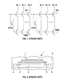
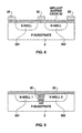
- the Caywood approach is illustrated in general terms for a single memory transistor 1.
- the N-well 3 is created within a P-type substrate 2.
- the P-channel for the drain 4 and source 5 is created within the N-well 3.
- Poly 1 or the floating gate 6 of the memory transistor 1 is created after the active region for the drain 4 and source 5.
- Poly2 or the control electrode 7 of the memory transistor is fabricated over the floating gate.
- Various nonconductive layers 8 insulate the P-channel 4 and 5, the floating gate 6 and the control electrode 7 from each other.
- Figure 3 illustrates a plurality of cell rows 100, typically connected to gate electrodes of memory transistors and a plurality of columns 200 typically connected to source and drain electrodes of memory transistors in the array, with both cell rows and cell columns existing on a single N-well 300 substrate.
- the limitation to the Caywood P-channel memory arrays, as shown in figure 3 is that all memory cells in any particular row must selected, thus written or erased, during a particular operation.
- the cell rows are not segmented such that some memory cells in the cell row may be selected for writing while other memory cells in the row are not.
- the entire cell row must then be programmed in order to change the data in one memory cell.
- One method of creating a plurality of N-wells within a substrate is referred to as p-n junction isolation.
- a method for segmenting the N-well of the memory array is referred to as dielectric isolation.
- a memory array comprises a plurality of N-wells within a P-type substrate and a plurality of independently programmable memory segments.
- Each independently programmable memory segment is comprised of M memory cell columns and N memory cell rows.
- Each independently programmable memory segment resides within a unique and separate N-well.
- each N-well contains an independently programmable memory segment.
- the method of creating the plurality of N-wells within the P-type substrate comprises the steps of growing a buffer oxide on a P-type substrate, applying photoresist to the buffer oxide, etching the photoresist to form a plurality of N-well channels and implanting N-wells via the N-well channels.
- a memory array comprises an N-well within a P-type substrate wherein the N-well is segmented in to a plurality of electrically isolated sub N-wells, M memory transistor columns within each of the plurality of electrically isolated sub N-wells and N memory transistor rows within each of the plurality of electrically isolated sub N-wells.
- the method of fabricating the sub-wells from a single N-well comprises the steps of implanting a P-type substrate to form a single N-well, applying photoresist over the single N-well, etching the photoresist to form a plurality of apertures, etching a plurality of trenches via the plurality of apertures with a trench depth which exceeds that of the N-well and which penetrates the P-type substrate to form a plurality of electrically isolated sub N-wells, and filling the plurality of trenches with an insulating material wherein the insulating material prevents electrical conduction as between each of the plurality of electrically isolated sub N-wells.
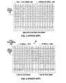
- a P-channel memory array 10 comprising a plurality of N-wells within a P-type substrate and a plurality of independently programmable memory segments is shown.
- Each independently programmable memory segment is comprised of a matrix of memory cell transistors shown as cell rows 100 and cell columns 200.
- the embodiment of figure 4 segments the 16 cell columns 200 and the plurality of cell rows 100 of the memory array 10 into two independently programmable memory segments residing within N-wells 301 and 302, respectively and shown in dashed lines.
- N-wells 301 and 302 are electrically separated from each other.
- each N-well segment there are eight memory transistor columns within each N-well segment, thereby comprising byte segments.
- N rows of memory transistors are illustrated. Not shown in figure 4 , but discussed below and shown in subsequent diagrams, are select transistors for assisting in control of the operation of the array 10.
- each of the independently programmable memory segments which may be comprised of M cell columns, where M is either smaller or larger than a byte.
- the number of cell columns M 200 alternative to the byte format, include, but are not limited to: 2, 4, 16, 32 and 64 cell columns 200 for each independently programmable memory segment.
- Each independently programmable memory segment is comprised of a plurality of independently programmable memory units.
- An independently programmable memory unit is defined as those cell columns 200 which are common to a given cell row 100 and within a single independently programmable memory segment. The intersection of a cell column 200 and a cell row 100 defines a memory cell which may be a single memory transistor as illustrated in figures 5-7 .
- each independently programmable memory unit is comprised of eight memory cells.
- the total number of independently programmable memory units for a given independently programmable memory segment is equal to the total number (N) of cell rows 100.
- independently programmable memory unit defines the smallest or most narrow portion of the memory array 10 that may be addressed by the write and erase memory operations described below. Additionally, all independently programmable memory units within a common cell row 100 may be simultaneously addressed by the write and erase memory operations.
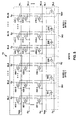
- FIG. 5 a write operation of the present invention is illustrated for the two byte segmentation embodiment of figure 4 .
- the present invention as illustrated in figure 5 , eliminates the byte select transistors which were necessary in the NMOS prior art.
- the row select circuity is outside of the memory array 10.
- the "pass gate,” sometimes referred to as the "select gate” transistor is merged into the memory cell, which is referred to as a "split cell.”
- the memory array 10 is comprised of a plurality of P-channel memory transistors 401-1 to 416-n which are laid out in a typical column/row matrix. Also shown are a row of P-channel source select transistors 501-516. Only one source select transistor 501-516 is necessary for each bit line BL1-BL16.
- N-well 301 Two separate N-wells with accompanying, independently programmable memory segments are shown in dashed lines drawn around a group of cells. Contained within N-well 301 are 8 memory transistor columns (only three are shown for clarity) and N memory transistor rows. N-well 302 is identical to N-well 301, however, N-well 302 is electrically isolated from N-well 301. Note that each independently programmable memory segment corresponds to an N-well and thus, the quantity of N-wells is equal to the quantity of independently programmable memory segments.
- the upper left independently programmable memory unit in N-well 301 is enclosed in a solid line box to indicate that this is the target independently programmable memory unit (i.e. target byte) for the write, erase, and read operations described below.
- target independently programmable memory unit i.e. target byte
- the control electrodes of the P-channel memory transistors 401-1 to 416-n for each row are connected to a common word line (WL).
- the word line may be either at ground potential, i.e. zero volts, or at some relatively high programming voltage V PP i.e. typically 12-20 volts.
- V PP programming voltage
- the control electrodes of memory transistors 401-1 to 416-1 are driven to V PP via WL1.
- the N-well 301 and the control electrodes of memory transistors 401-2 to 408-2 are set to ground potential or zero volts, tinder these conditions, no tunneling occurs because of an absence of an electric field. Thus, memory transistors 401-2 to 408-2 are not programmed, i.e. written to.
- the N-well 302 is at V PP and the control electrodes are ground potential which results in a P-type inversion layer under the poly2 layer of each of the memory cells 409-2 to 416-2.
- the control electrodes are ground potential which results in a P-type inversion layer under the poly2 layer of each of the memory cells 409-2 to 416-2.
- the drain electrodes of the memory transistors of any particular column are connected to a common bit, line (BL).
- BL bit, line
- the bit line to each of the columns BL1:8 and BL9:16 are set a zero volts.
- the source electrodes of each memory transistor in a particular column are commonly connected to a source select transistor 501-516.
- the source select transistors 501-516 are controlled by two select lines, SL1 and SL2.
- SL1 is set to V PP
- SL2 is set to ground potential.
- the N-well 301 is biased to ground potential. This permits a sufficient voltage potential between the floating gate of the memory transistors 401-1 to 408-1, controlled by WL1 and the N-well 301. Electrons tunnel from the N-well 301 across the dielectric layer to the floating gate where a charge is deposited, thus effecting the write cycle (refer to figure 2 ). Conversely, N-well 302 is biased to V PP , thereby failing to create the sufficient voltage potential between the control electrodes of the memory transistors 409-1 to 416-1 that are within N-well 302. Without a sufficient voltage differential, tunneling cannot occur and the write cycle is not accomplished.
- the P-channel memory transistors in any row may be organized in byte selectable segments where byte selection is effected, at least in part, by the application of, or biasing at, different voltage potentials, the plurality of the N-wells themselves.
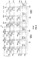
- word line WL1 is set to ground potential, which capacitively couples the floating gate of memory transistors 401-1 to 416-1 to a low voltage and turns the transistors on hard, thereby creating an inversion layer.
- the remainder of the word lines WL2:n, the select lines SL1:2 and N-wells 301 and 302 are biased to V PP .
- Bit lines BL1:8 for N-well 301 are set to V PP which biases the inversion layer under the floating gate to V PP . This causes electron tunneling from the floating gate to the inversion region in the N-well 301 and serves to remove the charge from the floating gate of the memory transistors 401-1 to 408-1 (refer to figure 2 ).
- a binary pattern may be entered in to the memory cells 401-1 through 408-1 by setting bit lines BL1-BL8 to either zero volts or V PP . Bit lines set to V PP will erase the memory cell. Bit lines set to zero volts will remain in the write or programming state.
- WL1 is set to V GR , a voltage between V DD and ground, sufficient to turn on memory transistors 401-1 to 416-1.
- Word lines WL2:n are set to V DD (typically 5 volts) which turn off the remainder of the memory transistors.
- the N-wells 301 and 302 are also set to V DD which is a normal "body bias" for a P-channel transistor in CMOS technology.
- SL1 is set to ground potential, thereby turning on the source select transistors.
- SL2 is set to V DD which permits the select transistors to source current.
- bit lines BL1:16 are left to control the read operation.
- BL1:BL8 are set to V DD V R (V R is a range 1.0 to 1.5 volts) which creates a voltage potential between the source and drain of the memory transistors resulting a current which is read by the sense amplifiers (not shown).
- BL9:16 are set to V DD , thereby not creating the requisite voltage potential between source and drain and thus, inhibiting the memory read of that byte.
- FIG. 8 illustrates the result of this process before the photoresist 20 is removed.
- the process begins with a P-substrate 2 upon which an implant buffer oxide 22 is grown.
- the photoresist 20 is applied and etched to form the channels for the implant.
- the formation of the two N-wells 301 and 302 by implantation occurs.
- the photoresist 20 is then removed and the remainder of the device is fabricated.
- the N-wells 301 and 302 are isolated from one another due to the p-n junction formed with the P-substrate in which they are implanted.
- P-type material may be implanted between the N-wells to increase the doping concentration between the implants. This will reduce the extent of the lateral N-well diffusion and decrease the width of depletion regions into the P-type material.
- a thick field oxide would be formed between active regions in the N-wells and would exist over the P-type region between the N-wells.
- trench etch and dielectric fill is an example of the dielectric isolation method for creating multiple sub-wells 301 a and 302a from an original, single N-well and minimizing the spacing between the sub-wells.
- the sub-wells 301a and 302a are separated by first forming one large N-well and then etching a deep trench 30 into the silicon substrate 2 to divide the N-well into the requisite number and size sub-wells.
- the side walls of the trenches may require implants and oxidation, or other passivation steps, to achieve good electrical characteristics for the junctions which abut them.
- the trenches are then filled with insulating material 32 or a combination of materials that prevent electrical conduction between the various N-wells.
Landscapes
- Engineering & Computer Science (AREA)
- Microelectronics & Electronic Packaging (AREA)
- Non-Volatile Memory (AREA)
- Semiconductor Memories (AREA)
- Metal-Oxide And Bipolar Metal-Oxide Semiconductor Integrated Circuits (AREA)
Applications Claiming Priority (3)
| Application Number | Priority Date | Filing Date | Title |
|---|---|---|---|
| US09/272,675 US6300183B1 (en) | 1999-03-19 | 1999-03-19 | Independently programmable memory segments within a PMOS electrically erasable programmable read only memory array achieved by N-well separation and method therefor |
| EP00918141A EP1090425B1 (fr) | 1999-03-19 | 2000-03-17 | Procédés de fabrication de segments de mémoire indépendamment programmables dans des caissons de type N isolés dans un dispositif EEPORM du type PMOS |
| PCT/US2000/007303 WO2000057476A1 (fr) | 1999-03-19 | 2000-03-17 | Segments de memoire independamment programmables dans des caissons d'isolement n isoles d'un reseau eeprom pmos et procede afferent |
Related Parent Applications (2)
| Application Number | Title | Priority Date | Filing Date |
|---|---|---|---|
| EP00918141.3 Division | 2000-03-17 | ||
| EP00918141A Division EP1090425B1 (fr) | 1999-03-19 | 2000-03-17 | Procédés de fabrication de segments de mémoire indépendamment programmables dans des caissons de type N isolés dans un dispositif EEPORM du type PMOS |
Publications (3)
| Publication Number | Publication Date |
|---|---|
| EP2267775A2 true EP2267775A2 (fr) | 2010-12-29 |
| EP2267775A3 EP2267775A3 (fr) | 2011-05-04 |
| EP2267775B1 EP2267775B1 (fr) | 2018-12-05 |
Family
ID=23040791
Family Applications (2)
| Application Number | Title | Priority Date | Filing Date |
|---|---|---|---|
| EP10180499.5A Expired - Lifetime EP2267775B1 (fr) | 1999-03-19 | 2000-03-17 | Segments de mémoire programmables de manière indépendante dans des puits isolés de type n à l'intérieur d'un dispositif eeprom du type pmos |
| EP00918141A Expired - Lifetime EP1090425B1 (fr) | 1999-03-19 | 2000-03-17 | Procédés de fabrication de segments de mémoire indépendamment programmables dans des caissons de type N isolés dans un dispositif EEPORM du type PMOS |
Family Applications After (1)
| Application Number | Title | Priority Date | Filing Date |
|---|---|---|---|
| EP00918141A Expired - Lifetime EP1090425B1 (fr) | 1999-03-19 | 2000-03-17 | Procédés de fabrication de segments de mémoire indépendamment programmables dans des caissons de type N isolés dans un dispositif EEPORM du type PMOS |
Country Status (7)
| Country | Link |
|---|---|
| US (2) | US6300183B1 (fr) |
| EP (2) | EP2267775B1 (fr) |
| JP (1) | JP2002540601A (fr) |
| KR (1) | KR20010025071A (fr) |
| CN (1) | CN1310863A (fr) |
| TW (1) | TW495975B (fr) |
| WO (1) | WO2000057476A1 (fr) |
Cited By (9)
| Publication number | Priority date | Publication date | Assignee | Title |
|---|---|---|---|---|
| WO2015108903A1 (fr) | 2014-01-16 | 2015-07-23 | Microchip Technology Incorporated | Dispositif mos à double diffusion et haute tension (dmos) et procédé de fabrication |
| US9269606B2 (en) | 2014-02-19 | 2016-02-23 | Microchip Technology Incorporated | Spacer enabled active isolation for an integrated circuit device |
| US9318702B2 (en) | 2014-02-19 | 2016-04-19 | Microchip Technology Incorporated | Resistive memory cell having a reduced conductive path area |
| US9349950B2 (en) | 2013-03-13 | 2016-05-24 | Microchip Technology Incorporated | Resistive memory cell with trench-shaped bottom electrode |
| US9385313B2 (en) | 2014-02-19 | 2016-07-05 | Microchip Technology Incorporated | Resistive memory cell having a reduced conductive path area |
| US9412942B2 (en) | 2014-02-19 | 2016-08-09 | Microchip Technology Incorporated | Resistive memory cell with bottom electrode having a sloped side wall |
| US9444040B2 (en) | 2013-03-13 | 2016-09-13 | Microchip Technology Incorporated | Sidewall type memory cell |
| US9865813B2 (en) | 2014-02-19 | 2018-01-09 | Microchip Technology Incorporated | Method for forming resistive memory cell having a spacer region under an electrolyte region and a top electrode |
| US10003021B2 (en) | 2014-02-19 | 2018-06-19 | Microchip Technology Incorporated | Resistive memory cell with sloped bottom electrode |
Families Citing this family (11)
| Publication number | Priority date | Publication date | Assignee | Title |
|---|---|---|---|---|
| US6300183B1 (en) * | 1999-03-19 | 2001-10-09 | Microchip Technology Incorporated | Independently programmable memory segments within a PMOS electrically erasable programmable read only memory array achieved by N-well separation and method therefor |
| EP1137012B1 (fr) * | 2000-03-22 | 2006-08-23 | Microchip Technology Inc. | Procédé de programmation amélioré pour une cellule de mémoire |
| DE10239491A1 (de) * | 2002-08-28 | 2004-03-18 | Infineon Technologies Ag | Verfahren zur Herstellung vergrabener Bitleitungen in einem Halbleiterspeicher |
| US7092288B2 (en) * | 2004-02-04 | 2006-08-15 | Atmel Corporation | Non-volatile memory array with simultaneous write and erase feature |
| US20070140008A1 (en) * | 2005-12-21 | 2007-06-21 | Microchip Technology Incorporated | Independently programmable memory segments within an NMOS electrically erasable programmable read only memory array achieved by P-well separation and method therefor |
| US7466591B2 (en) | 2006-06-01 | 2008-12-16 | Microchip Technology Incorporated | Method for programming and erasing an array of NMOS EEPROM cells that minimizes bit disturbances and voltage withstand requirements for the memory array and supporting circuits |
| US7817474B2 (en) * | 2006-06-01 | 2010-10-19 | Microchip Technology Incorporated | Method for programming and erasing an array of NMOS EEPROM cells that minimizes bit disturbances and voltage withstand requirements for the memory array and supporting circuits |
| US20090141554A1 (en) * | 2007-11-30 | 2009-06-04 | Atmel Corporation | Memory device having small array area |
| US8339862B2 (en) | 2007-12-25 | 2012-12-25 | Genusion, Inc. | Nonvolatile semiconductor memory device |
| JP5983236B2 (ja) * | 2012-09-25 | 2016-08-31 | 株式会社ソシオネクスト | 半導体記憶装置 |
| US10910058B2 (en) | 2018-08-17 | 2021-02-02 | Microchip Technology Incorporated | Shared source line memory architecture for flash cell byte-alterable high endurance data memory |
Citations (1)
| Publication number | Priority date | Publication date | Assignee | Title |
|---|---|---|---|---|
| US5790455A (en) | 1997-01-02 | 1998-08-04 | John Caywood | Low voltage single supply CMOS electrically erasable read-only memory |
Family Cites Families (14)
| Publication number | Priority date | Publication date | Assignee | Title |
|---|---|---|---|---|
| US4318751A (en) * | 1980-03-13 | 1982-03-09 | International Business Machines Corporation | Self-aligned process for providing an improved high performance bipolar transistor |
| US5170374A (en) * | 1981-05-13 | 1992-12-08 | Hitachi, Ltd. | Semiconductor memory |
| US4933295A (en) * | 1987-05-08 | 1990-06-12 | Raytheon Company | Method of forming a bipolar transistor having closely spaced device regions |
| US4851361A (en) * | 1988-02-04 | 1989-07-25 | Atmel Corporation | Fabrication process for EEPROMS with high voltage transistors |
| JP2655765B2 (ja) | 1991-05-29 | 1997-09-24 | ローム株式会社 | 半導体装置 |
| US5521108A (en) * | 1993-09-15 | 1996-05-28 | Lsi Logic Corporation | Process for making a conductive germanium/silicon member with a roughened surface thereon suitable for use in an integrated circuit structure |
| US5521105A (en) * | 1994-08-12 | 1996-05-28 | United Microelectronics Corporation | Method of forming counter-doped island in power MOSFET |
| US5736764A (en) | 1995-11-21 | 1998-04-07 | Programmable Microelectronics Corporation | PMOS flash EEPROM cell with single poly |
| JPH1083689A (ja) * | 1996-09-10 | 1998-03-31 | Mitsubishi Electric Corp | 不揮発性半導体記憶装置 |
| JP3712150B2 (ja) * | 1996-10-25 | 2005-11-02 | 株式会社日立製作所 | 半導体集積回路装置 |
| US5858839A (en) * | 1996-11-20 | 1999-01-12 | Texas Instruments Incorporated | Method of making EPROM cell array using n-tank as common source |
| JPH113595A (ja) | 1997-06-13 | 1999-01-06 | Sharp Corp | 不揮発性半導体記憶装置 |
| JPH11177069A (ja) | 1997-12-10 | 1999-07-02 | Matsushita Electron Corp | 不揮発性半導体記憶装置およびその書き換え方法 |
| US6300183B1 (en) * | 1999-03-19 | 2001-10-09 | Microchip Technology Incorporated | Independently programmable memory segments within a PMOS electrically erasable programmable read only memory array achieved by N-well separation and method therefor |
-
1999
- 1999-03-19 US US09/272,675 patent/US6300183B1/en not_active Expired - Lifetime
-
2000
- 2000-03-17 CN CN00800610A patent/CN1310863A/zh active Pending
- 2000-03-17 WO PCT/US2000/007303 patent/WO2000057476A1/fr not_active Ceased
- 2000-03-17 EP EP10180499.5A patent/EP2267775B1/fr not_active Expired - Lifetime
- 2000-03-17 JP JP2000607269A patent/JP2002540601A/ja not_active Withdrawn
- 2000-03-17 EP EP00918141A patent/EP1090425B1/fr not_active Expired - Lifetime
- 2000-03-17 KR KR1020007013048A patent/KR20010025071A/ko not_active Withdrawn
- 2000-05-04 TW TW089104866A patent/TW495975B/zh not_active IP Right Cessation
-
2001
- 2001-10-08 US US09/972,563 patent/US6504191B2/en not_active Expired - Lifetime
Patent Citations (1)
| Publication number | Priority date | Publication date | Assignee | Title |
|---|---|---|---|---|
| US5790455A (en) | 1997-01-02 | 1998-08-04 | John Caywood | Low voltage single supply CMOS electrically erasable read-only memory |
Cited By (16)
| Publication number | Priority date | Publication date | Assignee | Title |
|---|---|---|---|---|
| US9444040B2 (en) | 2013-03-13 | 2016-09-13 | Microchip Technology Incorporated | Sidewall type memory cell |
| US9349950B2 (en) | 2013-03-13 | 2016-05-24 | Microchip Technology Incorporated | Resistive memory cell with trench-shaped bottom electrode |
| US10056545B2 (en) | 2013-03-13 | 2018-08-21 | Microchip Technology Incorporated | Sidewall-type memory cell |
| US9362496B2 (en) | 2013-03-13 | 2016-06-07 | Microchip Technology Incorporated | Resistive memory cell with trench-shaped bottom electrode |
| US9601615B2 (en) | 2014-01-16 | 2017-03-21 | Microchip Technology Incorporated | High voltage double-diffused MOS (DMOS) device and method of manufacture |
| WO2015108903A1 (fr) | 2014-01-16 | 2015-07-23 | Microchip Technology Incorporated | Dispositif mos à double diffusion et haute tension (dmos) et procédé de fabrication |
| US9786779B2 (en) | 2014-01-16 | 2017-10-10 | Microchip Technology Incorporated | High voltage double-diffused MOS (DMOS) device and method of manufacture |
| US9306055B2 (en) | 2014-01-16 | 2016-04-05 | Microchip Technology Incorporated | High voltage double-diffused MOS (DMOS) device and method of manufacture |
| US9318702B2 (en) | 2014-02-19 | 2016-04-19 | Microchip Technology Incorporated | Resistive memory cell having a reduced conductive path area |
| US9269606B2 (en) | 2014-02-19 | 2016-02-23 | Microchip Technology Incorporated | Spacer enabled active isolation for an integrated circuit device |
| US9385313B2 (en) | 2014-02-19 | 2016-07-05 | Microchip Technology Incorporated | Resistive memory cell having a reduced conductive path area |
| US9412942B2 (en) | 2014-02-19 | 2016-08-09 | Microchip Technology Incorporated | Resistive memory cell with bottom electrode having a sloped side wall |
| US9865814B2 (en) | 2014-02-19 | 2018-01-09 | Microchip Technology Incorporated | Resistive memory cell having a single bottom electrode and two top electrodes |
| US9865813B2 (en) | 2014-02-19 | 2018-01-09 | Microchip Technology Incorporated | Method for forming resistive memory cell having a spacer region under an electrolyte region and a top electrode |
| US9917251B2 (en) | 2014-02-19 | 2018-03-13 | Microchip Technology Incorporated | Resistive memory cell having a reduced conductive path area |
| US10003021B2 (en) | 2014-02-19 | 2018-06-19 | Microchip Technology Incorporated | Resistive memory cell with sloped bottom electrode |
Also Published As
| Publication number | Publication date |
|---|---|
| US6300183B1 (en) | 2001-10-09 |
| EP1090425B1 (fr) | 2012-06-27 |
| TW495975B (en) | 2002-07-21 |
| CN1310863A (zh) | 2001-08-29 |
| WO2000057476A1 (fr) | 2000-09-28 |
| JP2002540601A (ja) | 2002-11-26 |
| EP2267775B1 (fr) | 2018-12-05 |
| EP1090425A1 (fr) | 2001-04-11 |
| EP2267775A3 (fr) | 2011-05-04 |
| KR20010025071A (ko) | 2001-03-26 |
| US20020014642A1 (en) | 2002-02-07 |
| US6504191B2 (en) | 2003-01-07 |
Similar Documents
| Publication | Publication Date | Title |
|---|---|---|
| EP1090425B1 (fr) | Procédés de fabrication de segments de mémoire indépendamment programmables dans des caissons de type N isolés dans un dispositif EEPORM du type PMOS | |
| EP2339585B1 (fr) | mémoire EEPROM | |
| USRE39697E1 (en) | Method of making floating-gate memory-cell array with digital logic transistors | |
| EP0819308A1 (fr) | Programmation flash d'une memoire flash de type eeprom | |
| US20040197993A1 (en) | Non-volatile memory integrated circuit | |
| US5432740A (en) | Low voltage flash EEPROM memory cell with merge select transistor and non-stacked gate structure | |
| EP0637035B1 (fr) | Structure de circuit pour matrice de mémoire et procédé de fabrication y reférant | |
| EP2368250B1 (fr) | Procédé de programmation et d'effacement d'une matrice de cellules mémoires(eeprom) nmos permettant de réduire les perturbations sur les bits et les exigences de tenue en tension pour la matrice mémoire et les circuits de mise en uvre | |
| WO2007078614A1 (fr) | Segments de mémoire programmables indépendamment dans une matrice de mémoire morte effaçable et programmable électriquement nmos, réalisés par une séparation de puits p et procédé pour ceux-ci | |
| KR19990024472A (ko) | 고속 재기록용 비휘발성 메모리 장치 및 그 제조 방법 |
Legal Events
| Date | Code | Title | Description |
|---|---|---|---|
| PUAI | Public reference made under article 153(3) epc to a published international application that has entered the european phase |
Free format text: ORIGINAL CODE: 0009012 |
|
| 17P | Request for examination filed |
Effective date: 20100927 |
|
| AC | Divisional application: reference to earlier application |
Ref document number: 1090425 Country of ref document: EP Kind code of ref document: P |
|
| AK | Designated contracting states |
Kind code of ref document: A2 Designated state(s): AT BE CH CY DE DK ES FI FR GB GR IE IT LI LU MC NL PT SE |
|
| PUAL | Search report despatched |
Free format text: ORIGINAL CODE: 0009013 |
|
| AK | Designated contracting states |
Kind code of ref document: A3 Designated state(s): AT BE CH CY DE DK ES FI FR GB GR IE IT LI LU MC NL PT SE |
|
| RIC1 | Information provided on ipc code assigned before grant |
Ipc: H01L 21/8247 20060101ALI20110331BHEP Ipc: G11C 16/04 20060101ALI20110331BHEP Ipc: H01L 27/115 20060101AFI20101119BHEP Ipc: H01L 27/02 20060101ALN20110331BHEP |
|
| 17Q | First examination report despatched |
Effective date: 20120504 |
|
| REG | Reference to a national code |
Ref country code: DE Ref legal event code: R079 Ref document number: 60049890 Country of ref document: DE Free format text: PREVIOUS MAIN CLASS: H01L0027115000 Ipc: H01L0027115210 |
|
| GRAP | Despatch of communication of intention to grant a patent |
Free format text: ORIGINAL CODE: EPIDOSNIGR1 |
|
| STAA | Information on the status of an ep patent application or granted ep patent |
Free format text: STATUS: GRANT OF PATENT IS INTENDED |
|
| RIC1 | Information provided on ipc code assigned before grant |
Ipc: G11C 16/04 20060101ALI20180622BHEP Ipc: H01L 27/11521 20170101AFI20180622BHEP |
|
| INTG | Intention to grant announced |
Effective date: 20180718 |
|
| GRAS | Grant fee paid |
Free format text: ORIGINAL CODE: EPIDOSNIGR3 |
|
| GRAA | (expected) grant |
Free format text: ORIGINAL CODE: 0009210 |
|
| GRAA | (expected) grant |
Free format text: ORIGINAL CODE: 0009210 |
|
| STAA | Information on the status of an ep patent application or granted ep patent |
Free format text: STATUS: THE PATENT HAS BEEN GRANTED |
|
| AC | Divisional application: reference to earlier application |
Ref document number: 1090425 Country of ref document: EP Kind code of ref document: P |
|
| AK | Designated contracting states |
Kind code of ref document: B1 Designated state(s): AT BE CH CY DE DK ES FI FR GB GR IE IT LI LU MC NL PT SE |
|
| REG | Reference to a national code |
Ref country code: GB Ref legal event code: FG4D |
|
| REG | Reference to a national code |
Ref country code: CH Ref legal event code: EP |
|
| REG | Reference to a national code |
Ref country code: AT Ref legal event code: REF Ref document number: 1074125 Country of ref document: AT Kind code of ref document: T Effective date: 20181215 |
|
| REG | Reference to a national code |
Ref country code: IE Ref legal event code: FG4D |
|
| REG | Reference to a national code |
Ref country code: DE Ref legal event code: R096 Ref document number: 60049890 Country of ref document: DE |
|
| REG | Reference to a national code |
Ref country code: NL Ref legal event code: MP Effective date: 20181205 |
|
| REG | Reference to a national code |
Ref country code: AT Ref legal event code: MK05 Ref document number: 1074125 Country of ref document: AT Kind code of ref document: T Effective date: 20181205 |
|
| PG25 | Lapsed in a contracting state [announced via postgrant information from national office to epo] |
Ref country code: ES Free format text: LAPSE BECAUSE OF FAILURE TO SUBMIT A TRANSLATION OF THE DESCRIPTION OR TO PAY THE FEE WITHIN THE PRESCRIBED TIME-LIMIT Effective date: 20181205 Ref country code: AT Free format text: LAPSE BECAUSE OF FAILURE TO SUBMIT A TRANSLATION OF THE DESCRIPTION OR TO PAY THE FEE WITHIN THE PRESCRIBED TIME-LIMIT Effective date: 20181205 Ref country code: FI Free format text: LAPSE BECAUSE OF FAILURE TO SUBMIT A TRANSLATION OF THE DESCRIPTION OR TO PAY THE FEE WITHIN THE PRESCRIBED TIME-LIMIT Effective date: 20181205 |
|
| PGFP | Annual fee paid to national office [announced via postgrant information from national office to epo] |
Ref country code: DE Payment date: 20190219 Year of fee payment: 20 |
|
| PG25 | Lapsed in a contracting state [announced via postgrant information from national office to epo] |
Ref country code: SE Free format text: LAPSE BECAUSE OF FAILURE TO SUBMIT A TRANSLATION OF THE DESCRIPTION OR TO PAY THE FEE WITHIN THE PRESCRIBED TIME-LIMIT Effective date: 20181205 Ref country code: GR Free format text: LAPSE BECAUSE OF FAILURE TO SUBMIT A TRANSLATION OF THE DESCRIPTION OR TO PAY THE FEE WITHIN THE PRESCRIBED TIME-LIMIT Effective date: 20190306 |
|
| PGFP | Annual fee paid to national office [announced via postgrant information from national office to epo] |
Ref country code: FR Payment date: 20190219 Year of fee payment: 20 |
|
| PG25 | Lapsed in a contracting state [announced via postgrant information from national office to epo] |
Ref country code: NL Free format text: LAPSE BECAUSE OF FAILURE TO SUBMIT A TRANSLATION OF THE DESCRIPTION OR TO PAY THE FEE WITHIN THE PRESCRIBED TIME-LIMIT Effective date: 20181205 |
|
| PG25 | Lapsed in a contracting state [announced via postgrant information from national office to epo] |
Ref country code: PT Free format text: LAPSE BECAUSE OF FAILURE TO SUBMIT A TRANSLATION OF THE DESCRIPTION OR TO PAY THE FEE WITHIN THE PRESCRIBED TIME-LIMIT Effective date: 20190405 Ref country code: IT Free format text: LAPSE BECAUSE OF FAILURE TO SUBMIT A TRANSLATION OF THE DESCRIPTION OR TO PAY THE FEE WITHIN THE PRESCRIBED TIME-LIMIT Effective date: 20181205 |
|
| REG | Reference to a national code |
Ref country code: DE Ref legal event code: R097 Ref document number: 60049890 Country of ref document: DE |
|
| PLBE | No opposition filed within time limit |
Free format text: ORIGINAL CODE: 0009261 |
|
| STAA | Information on the status of an ep patent application or granted ep patent |
Free format text: STATUS: NO OPPOSITION FILED WITHIN TIME LIMIT |
|
| PG25 | Lapsed in a contracting state [announced via postgrant information from national office to epo] |
Ref country code: DK Free format text: LAPSE BECAUSE OF FAILURE TO SUBMIT A TRANSLATION OF THE DESCRIPTION OR TO PAY THE FEE WITHIN THE PRESCRIBED TIME-LIMIT Effective date: 20181205 Ref country code: MC Free format text: LAPSE BECAUSE OF FAILURE TO SUBMIT A TRANSLATION OF THE DESCRIPTION OR TO PAY THE FEE WITHIN THE PRESCRIBED TIME-LIMIT Effective date: 20181205 |
|
| REG | Reference to a national code |
Ref country code: CH Ref legal event code: PL |
|
| 26N | No opposition filed |
Effective date: 20190906 |
|
| GBPC | Gb: european patent ceased through non-payment of renewal fee |
Effective date: 20190317 |
|
| PG25 | Lapsed in a contracting state [announced via postgrant information from national office to epo] |
Ref country code: LU Free format text: LAPSE BECAUSE OF NON-PAYMENT OF DUE FEES Effective date: 20190317 |
|
| REG | Reference to a national code |
Ref country code: BE Ref legal event code: MM Effective date: 20190331 |
|
| PG25 | Lapsed in a contracting state [announced via postgrant information from national office to epo] |
Ref country code: GB Free format text: LAPSE BECAUSE OF NON-PAYMENT OF DUE FEES Effective date: 20190317 Ref country code: LI Free format text: LAPSE BECAUSE OF NON-PAYMENT OF DUE FEES Effective date: 20190331 Ref country code: IE Free format text: LAPSE BECAUSE OF NON-PAYMENT OF DUE FEES Effective date: 20190317 Ref country code: CH Free format text: LAPSE BECAUSE OF NON-PAYMENT OF DUE FEES Effective date: 20190331 |
|
| PG25 | Lapsed in a contracting state [announced via postgrant information from national office to epo] |
Ref country code: BE Free format text: LAPSE BECAUSE OF NON-PAYMENT OF DUE FEES Effective date: 20190331 |
|
| REG | Reference to a national code |
Ref country code: DE Ref legal event code: R071 Ref document number: 60049890 Country of ref document: DE |
|
| PG25 | Lapsed in a contracting state [announced via postgrant information from national office to epo] |
Ref country code: CY Free format text: LAPSE BECAUSE OF FAILURE TO SUBMIT A TRANSLATION OF THE DESCRIPTION OR TO PAY THE FEE WITHIN THE PRESCRIBED TIME-LIMIT Effective date: 20181205 |