EP2263248B1 - Source ionique à effet de champ utilisant du gaz et comprenant un embout revêtu - Google Patents
Source ionique à effet de champ utilisant du gaz et comprenant un embout revêtu Download PDFInfo
- Publication number
- EP2263248B1 EP2263248B1 EP09716494.1A EP09716494A EP2263248B1 EP 2263248 B1 EP2263248 B1 EP 2263248B1 EP 09716494 A EP09716494 A EP 09716494A EP 2263248 B1 EP2263248 B1 EP 2263248B1
- Authority
- EP
- European Patent Office
- Prior art keywords
- tip
- ion source
- coating
- electrically conductive
- conductive material
- Prior art date
- Legal status (The legal status is an assumption and is not a legal conclusion. Google has not performed a legal analysis and makes no representation as to the accuracy of the status listed.)
- Active
Links
Images


Classifications
-
- H—ELECTRICITY
- H01—ELECTRIC ELEMENTS
- H01J—ELECTRIC DISCHARGE TUBES OR DISCHARGE LAMPS
- H01J49/00—Particle spectrometers or separator tubes
- H01J49/02—Details
- H01J49/10—Ion sources; Ion guns
- H01J49/16—Ion sources; Ion guns using surface ionisation, e.g. field-, thermionic- or photo-emission
- H01J49/168—Ion sources; Ion guns using surface ionisation, e.g. field-, thermionic- or photo-emission field ionisation, e.g. corona discharge
-
- H—ELECTRICITY
- H01—ELECTRIC ELEMENTS
- H01J—ELECTRIC DISCHARGE TUBES OR DISCHARGE LAMPS
- H01J27/00—Ion beam tubes
- H01J27/02—Ion sources; Ion guns
- H01J27/26—Ion sources; Ion guns using surface ionisation, e.g. field effect ion sources, thermionic ion sources
-
- H—ELECTRICITY
- H01—ELECTRIC ELEMENTS
- H01J—ELECTRIC DISCHARGE TUBES OR DISCHARGE LAMPS
- H01J37/00—Discharge tubes with provision for introducing objects or material to be exposed to the discharge, e.g. for the purpose of examination or processing thereof
- H01J37/02—Details
- H01J37/04—Arrangements of electrodes and associated parts for generating or controlling the discharge, e.g. electron-optical arrangement, ion-optical arrangement
- H01J37/06—Electron sources; Electron guns
- H01J37/065—Construction of guns or parts thereof
-
- H—ELECTRICITY
- H01—ELECTRIC ELEMENTS
- H01J—ELECTRIC DISCHARGE TUBES OR DISCHARGE LAMPS
- H01J37/00—Discharge tubes with provision for introducing objects or material to be exposed to the discharge, e.g. for the purpose of examination or processing thereof
- H01J37/02—Details
- H01J37/04—Arrangements of electrodes and associated parts for generating or controlling the discharge, e.g. electron-optical arrangement, ion-optical arrangement
- H01J37/08—Ion sources; Ion guns
-
- H—ELECTRICITY
- H01—ELECTRIC ELEMENTS
- H01J—ELECTRIC DISCHARGE TUBES OR DISCHARGE LAMPS
- H01J37/00—Discharge tubes with provision for introducing objects or material to be exposed to the discharge, e.g. for the purpose of examination or processing thereof
- H01J37/26—Electron or ion microscopes; Electron or ion diffraction tubes
- H01J37/28—Electron or ion microscopes; Electron or ion diffraction tubes with scanning beams
-
- H—ELECTRICITY
- H01—ELECTRIC ELEMENTS
- H01J—ELECTRIC DISCHARGE TUBES OR DISCHARGE LAMPS
- H01J2237/00—Discharge tubes exposing object to beam, e.g. for analysis treatment, etching, imaging
- H01J2237/06—Sources
- H01J2237/063—Electron sources
- H01J2237/06325—Cold-cathode sources
- H01J2237/06341—Field emission
-
- H—ELECTRICITY
- H01—ELECTRIC ELEMENTS
- H01J—ELECTRIC DISCHARGE TUBES OR DISCHARGE LAMPS
- H01J2237/00—Discharge tubes exposing object to beam, e.g. for analysis treatment, etching, imaging
- H01J2237/06—Sources
- H01J2237/08—Ion sources
- H01J2237/0802—Field ionization sources
- H01J2237/0807—Gas field ion sources [GFIS]
-
- H—ELECTRICITY
- H01—ELECTRIC ELEMENTS
- H01J—ELECTRIC DISCHARGE TUBES OR DISCHARGE LAMPS
- H01J2237/00—Discharge tubes exposing object to beam, e.g. for analysis treatment, etching, imaging
- H01J2237/26—Electron or ion microscopes
- H01J2237/28—Scanning microscopes
Definitions
- the disclosure generally relates to coated tips, as well as related articles, systems and methods.
- Gas field ion sources are known.
- a gas field ion source includes a tip formed of electrically conductive material.
- the tip can be used to ionize neutral gas species to generate ions by bringing the neutral gas species into the vicinity of the tip while applying a high positive potential to the apex of the tip.
- the ions can, for example, be formed into a beam that can be used to determine certain properties of a sample and/or to modify the sample.
- US 2003/122085A1 discloses a gas field ion source array including an array of tips positioned on a base plate and an extraction electrode.
- the tips are coated with DLC, single metal coatings or carbon nanotubes.
- US 2007/138388A1 discloses a gas field ion beam system with a gas field ion source comprising a tip being made of an electrically conductive material, the tip having an apex terminating in an atomic shelf having 20 atoms or less.
- the gas field ion source further comprises an extractor and means for biasing the tip with respect to the extractor to generate an electrical field at the apex of the tip directed outward from the surface of the apex.
- the tip can be coated with a coating
- US3911311A discloses a field desorption ion source comprising a gas permeable electrode which is coated on its surface with a gas impervious coating.
- the electrode comprises a tip portion where the coating has been removed so that gas to be ionized can diffuse through the electrode and become ionized in the vicinity of the tip.
- EP 1564774A1 and EP1947674A1 disclose thermionic or field emission electron sources comprising an electron emitting tip with a coating on the conical surface of the tip to avoid emission of electrons at the conical surface and to avoid sublimation and evaporation of the tip material.
- the present invention relates to a gas field ion source comprising the features of claim 1 and to a method for manufacturing a tip for a gas field ion source comprising the features of claim 11.
- the tip geometry can change, which can cause the field at the apex of the tip to increase to the point where it can exceed the field evaporation strength of the material that forms the tip, resulting in undesirable field evaporation of the atoms at the tip.
- undesirable corrosion can be reduced, and possibly even eliminated, by coating certain portions of the tip without coating other portions of the tip.
- tip corrosion can be controlled so that undesirable tip corrosion is limited.
- the disclosure features an article that includes a first electrically conductive material and a coating.
- the article is configured to be used as a tip in a gas field ion source.
- the coating is supported by the first electrically conductive material only where an average emission current density from the article is at most 50% of a maximum emission current density from the article when the article is being used as the tip in the gas field ion source.
- the disclosure provides an article that includes a first electrically conductive material having a surface and a coating.
- the article is configured to be used as a tip in a gas field ion source.
- the first electrically conductive material has a surface, and the coating is supported by the first electrically conductive material only where a normal to the surface of the first electrically conductive material is within 60° of an axis normal to an apex of the first electrically conductive material.
- the disclosure provides an article that includes a first electrically conductive material having a surface and a coating.
- the article is configured to be used as a tip in a gas field ion source.
- the first electrically conductive material has a surface.
- the coating is supported by the first electrically conductive material except within a distance of 200 nm of an apex of the first electrically conductive material as measured along the surface of the first electrically conductive material.
- the disclosure provides a method that includes forming a coating supported by an electrically conductive material, and removing a portion of the coating to provide an article.
- the article is configured to be used as a tip in a gas field ion source.
- the coating is supported by the first electrically conductive material only where an average emission current density from the article is at most 50% of a maximum emission current density from the article when the article is being used as the tip in the gas field ion source.
- the disclosure provides a method that includes forming a coating supported by a surface of an electrically conductive material, and removing a portion of the coating to provide an article.
- the article is configured to be used as a tip in a gas field ion source.
- the first electrically conductive material has a surface.
- the coating is supported by the first electrically conductive material only where a normal to the surface of the first electrically conductive material within 60° of an axis normal to an apex of the first electrically conductive material.
- the disclosure provides a method that includes forming a coating supported by a surface of an electrically conductive material, and removing a portion of the coating to provide an article.
- the article is configured to be used as a tip in a gas field ion source.
- the first electrically conductive material has a surface.
- the coating is supported by the first electrically conductive material except within a distance of 200 nm of an apex of the first electrically conductive material as measured along the surface of the first electrically conductive material.
- the disclosure provides an article that includes a first electrically conductive material having an apex, and a coating supported by the first electrically conductive material at a location other than the apex of the first electrically conductive material.
- the article is configured to be used as a tip in a gas field ion source.
- the disclosure provides a method that includes forming a coating supported by a surface of an electrically conductive material having an apex, and removing the coating from the apex of the electrically conductive material to provide an article.
- the article is configured to be used as a tip in a gas field ion source.
- Embodiments can provide one or more of the following advantages.
- the tip can provide enhanced reliability and/or use lifetime. This can, for example, result in improved performance when used as a particle source (e.g., as a source of ions in a gas field ion source, such as a gas field ion source).
- a particle source e.g., as a source of ions in a gas field ion source, such as a gas field ion source.
- the tip can be prepared by a process that involves desirable corrosion with little or no undesirable corrosion.
- Fig. 1 is a cross-sectional view of a portion of an electrically conductive tip 100 of a gas field ion source.
- tip 100 is made of an electrically conductive material, such as carbon, a metal or an alloy.
- Exemplary metals include gold, silver, palladium, osmium, tungsten, tantalum, iridium, rhenium, niobium, platinum and molybdenum.
- Exemplary alloys include at least two materials selected from carbon, gold, silver, palladium, osmium, tungsten, tantalum, iridium, rhenium, niobium, platinum and molybdenum.
- tip 100 can be formed of a single crystal material, such as a single crystal metal.
- a particular single crystal orientation of the terminal shelf of atoms of an apex 101 of tip 100 is aligned with a plane 103 which is tangent to the surface at the apex 101 to within 10° or less (e.g., within 5° or less, within 3° or less).
- apex 101 of tip 100 can terminate in an atomic shelf having a certain number of atoms (e.g., 20 atoms or less, 15 atoms or less, 10 atoms or less, nine atoms or less, six atoms or less, three atoms or less).
- apex 101 of tip 100 can be formed of W(111) and can have a terminal shelf with three atoms (a trimer).
- tip 100 can have a terminal shelf that includes fewer than three atoms or more than three atoms.
- a W(111) tip can have a terminal shelf that includes two atoms, or a terminal shelf that includes only one atom.
- a W(111) tip can have a terminal shelf that includes four or more atoms (e.g., five or more atoms, six or more atoms, seven or more atoms, eight or more atoms, nine or more atoms, ten or more atoms, more than ten atoms).
- tip 100 can correspond to a different W crystalline orientation, such as W(112), W(110) or W(100).
- a tip can have terminal shelves that include one or more atoms (e.g., two or more atoms, three or more atoms, four or more atoms, five or more atoms, six or more atoms, seven or more atoms, eight or more atoms, nine or more atoms, ten or more atoms, more than ten atoms).
- tip 100 can be formed from a material other than single crystal W (e.g., a single crystal of a metal, such as a single crystal of one of the metals noted above), and such a tip can have a terminal shelf that includes one or more atoms (e.g., two or more atoms, three or more atoms, four or more atoms, five or more atoms, six or more atoms, seven or more atoms, eight or more atoms, nine or more atoms, ten or more atoms, more than ten atoms).
- atoms e.g., two or more atoms, three or more atoms, four or more atoms, five or more atoms, six or more atoms, seven or more atoms, eight or more atoms, nine or more atoms, ten or more atoms, more than ten atoms.
- Tip 100 has a surface 102 with regions 104, 106 and 108.
- Region 104 has a relatively high average emission current and/or a relatively high average emission current density
- region 108 has a relatively low average emission current and/or a relatively low average emission current density.
- Region 106 has an intermediate average emission current and/or an intermediate average emission current density that is between that of regions 104 and 108.
- an angle ⁇ between a normal 105 to surface 102 and an axis 107 that is perpendicular to plane 103 is at most 60° (e.g., at most 45°, at most 30°).
- ⁇ is at least 15° (e.g., at least 25°, at least 30°).
- ⁇ can be from 15° to 60° (e.g., from 15° to 45°, from 15° to 30°, from 25° to 60°, from 25° to 45°, from 25° to 30°, from 30° to 60°, from 30° to 45°).
- the distance from an uppermost point 109 of region 106 to apex 101, as measured along surface 102 is at most 200 nm (e.g., at most 100 nm, at most 50 nm). In certain embodiments, the distance from point 109 to apex 101, as measured along surface 102, is at least 25 nm (e.g., at least 30 nm, at least 40 nm).
- the distance from an uppermost point 109 of region 106 to apex 101, as measured along surface 102 can be from 25 nm to 200 nm (e.g., from 25 nm to 100 nm, from 25 nm to 50 nm, from 30 nm to 200 nm, from 30 nm to 100 nm, from 30 nm to 50 nm, from 40 nm to 200 nm, from 40 nm to 100 nm, from 40 nm to 50 nm).
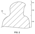
- Fig. 2 is a schematic representation of corrosion that can occur to tip 100 during use when a typical, high positive potential is applied to apex.
- Applicants believe that in region 108 the electric field is so low that gas atoms can reach region 108, and possible even adsorb to surface 102, but that most of the gas atoms do not undergo ionization and corrosion does not occur.
- Applicants believe that in region 104 the electric field is so high that most of the gas atoms are ionized and accelerated away from surface 102 without contacting surface 102.
- region 106 the electric field is sufficiently strong to attract gas atoms, but that the electric field is not strong enough to cause all the ions to be ionized accelerated away from tip 100 without contacting surface 102. Thus, many of the ions can interact with surface 102 in the region 106. Further, Applicants believe that in region 106 unique chemical reactions can take place on region 106 in the presence of the intermediate electric field which otherwise would not take place.
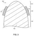
- Fig. 3 is a cross-sectional view of an article 300 that includes tip 100 and a coating 310 disposed on surface 102 of tip 100 only in region 106.
- the average emission current density of article 300 within region 106 is at most 50% (e.g., at most 25%, at most 10%) of the maximum emission current density of article 300 when article 300 is used as the tip in the gas field ion source, and the average emission current density of article 300 within region 106 is at least 1% (e.g., at least 5%, at least 10%) of the maximum emission current density of article 300 when article 300 is used as the tip in the gas field ion source.
- the average emission current density of article 300 within region 106 is from 1% to 50% (e.g., from 5% to 50%, from 10% to 50%, from 1% to 25%, from 1% to 10%, from 10% to 50%, from 10% to 25%) of the maximum emission current density of article 300 when article 300 is used as the tip in the gas field ion source.
- the maximum emission current density of article 300 when article is used as the tip in the gas field ion source is at most 10 pA/ ⁇ 2 (e.g., at most 1.0 pA/ ⁇ 2 , at most 0.1 pA/ ⁇ 2 ), and/or at least 0.001 pA/ ⁇ 2 (e.g., at least 0.01 pA/ ⁇ 2 , at least 0.1 pA/ ⁇ 2 ).
- coating 310 is formed of an electrically conductive material, such as carbon, a metal or an alloy.
- exemplary metals include gold, silver, palladium, osmium, tungsten, tantalum, iridium, rhenium, niobium, platinum and molybdenum.
- exemplary alloys include at least two metals selected from carbon, gold, silver, palladium, osmium, tungsten, tantalum, iridium, rhenium, niobium, platinum and molybdenum.
- coating 310 can be formed by any desired process.
- Exemplary processes include evaporation, liquid deposition, electrochemical deposition, chemical vapor deposition, physical vapor deposition, molecular beam deposition, plasma deposition.
- the material forming the coating is disposed on surface 102 only at region 106. In certain embodiments, this can be achieved by blocking regions 104 and 108 of surface 102 from exposure to the material that forms layer 310 (e.g., when the material is in a gaseous or solid state) during the formation of coating 310.
- the material forming the coating is disposed on more than only region 106 of surface 102 (e.g., on region 108 of surface 102 and/or on region 104 of surface 102), followed by removal of the material from other than region 106 of surface 102.
- the material that forms coating 310 may be disposed on more than region 104 of surface 102, and the article may be subsequently treated (e.g., by evaporation, sputtering, and/or etching) to remove the material from surface 102 in other than region 106.
- the removal of the material can be achieved by heating the article (e.g., to cause thermally-induced evaporation of the material from selected regions of surface 102).
- the removal of the material can be achieved by applying an electric field of appropriate strength to tip 100 (e.g., by using a high electric field near the apex to field evaporate material from region 104 of surface 102).
- This section discloses systems and methods for producing ion beams, and detecting particles including secondary electrons that leave a sample of interest due to exposure of the sample to an ion beam.
- the systems and methods can be used to obtain one or more images of the sample, and/or to modify the sample.
- Such ion beams are produced in multipurpose microscope systems.
- Microscope systems that use a gas field ion source to generate ions that can be used in sample analysis (e.g., imaging) and/or modification are referred to as gas field ion microscopes.
- a gas field ion source is a device that includes an electrically conductive tip (typically having an apex with 10 or fewer atoms) that can be used to ionize neutral gas species to generate ions (e.g., in the form of an ion beam) by bringing the neutral gas species into the vicinity of the electrically conductive tip (e.g., within a distance of about four to five angstroms) while applying a high positive potential (e.g., one kV or more relative to the extractor (see discussion below)) to the apex of the electrically conductive tip.
- a coating as described herein can be present on the tip.
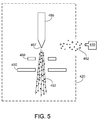
- Fig. 4 shows a schematic diagram of a gas field ion microscope system 400 that includes a gas source 410, a gas field ion source 420, ion optics 430, a sample manipulator 440, a frontside detector 450, a back-side detector 460, and an electronic control system 470 (e.g., an electronic processor, such as a computer) electrically connected to various components of system 400 via communication lines 472a-472f.
- a sample 480 is positioned in/on sample manipulator 440 between ion optics 430 and detectors 450, 460.
- an ion beam 492 is directed through ion optics 430 to a surface 481 of sample 480, and particles 494 resulting from the interaction of ion beam 492 with sample 480 are measured by detectors 450 and/or 460.
- the detected particles may include particles (such as secondary electrons, or auger electrons, or sputtered neutral atoms, or sputtered ions, or fast recoiled neutral atoms, or fast recoiled ions) which already existed within the sample prior to interacting with the ion beam, particles (such as photons, x-rays) which were created through the interaction of the ion beam with the sample, and/or particles (including backscattered helium ions, backscattered helium neutrals, transmitted and undeflected helium ions, transmitted and undeflected helium neutrals, transmitted and deflected helium ions, transmitted and deflected helium neutrals) which where were initially present in the incident ion beam.
- particles such as secondary electrons, or auger electrons, or sputtered neutral atoms, or sputtered ions, or fast recoiled neutral atoms, or fast recoiled ions
- particles such as photons, x-rays
- particles including back
- the background pressure rises to approximately 10 -4 Torr.
- Ion optics 430 are maintained at a background pressure of approximately 10 -8 Torr prior to the introduction of gas into gas field ion source 420.
- the background pressure in ion optics 430 typically increase to approximately 10 -7 Torr.
- Sample 480 is positioned within a chamber that is typically maintained at a background pressure of approximately 10 -6 Torr. This pressure does not vary significantly due to the presence or absence of gas in gas field ion source 420.
- gas source 410 is configured to supply one or more gases 482 to gas field ion source 420.
- gas source 410 can be configured to supply the gas(es) at a variety of purities, flow rates, pressures, and temperatures.
- at least one of the gases supplied by gas source 410 is a noble gas (helium (He), neon (Ne), argon (Ar), krypton (Kr), xenon (Xe)), and ions of the noble gas are desirably the primary constituent in ion beam 492.
- the current of ions in ion beam 492 increases monotonically as the pressure of the noble gas in system 400 increases.
- this relationship can be described by a power law where, for a certain range of noble gas pressures, the current increases generally in proportion to gas pressure.
- the pressure of the noble gas is typically 10 -2 Torr or less (e.g., 10 -3 Torr or less, 10 -4 Torr or less), and/or 10 -7 Torr or more (e.g., 10 -6 Torr or more, 10 -5 Torr or more) adjacent the tip apex (see discussion below).
- it is desirable to use relatively high purity gases e.g., to reduce the presence of undesirable chemical species in the system).
- gas source 410 can supply one or more gases in addition to the noble gas(es).
- an example of such a gas is nitrogen.
- the additional gas(es) can be present at levels above the level of impurities in the noble gas(es), the additional gas(es) still constitute minority components of the overall gas mixture introduced by gas source 410.
- the overall gas mixture can include 20% or less (e.g., 15% or less, 12% or less) Ne, and/or 1% or more (e.g., 3% or more, 8% or more) Ne.
- the overall gas mixture can include from 5% to 15% (e.g., from 8% to 12%, from 9% to 11%) Ne.
- the overall gas mixture can include 1% or less (e.g., 0.5% or less, 0.1% or less) nitrogen, and/or 0.01% or more (e.g., 0.05% or more) nitrogen.
- the overall gas mixture can include from 0.01% to 1% (e.g., from 0.05% to 0.5%, from 0.08 to 0.12%) nitrogen.
- the additional gas(es) are mixed with the noble gas(es) before entering system 400 (e.g., via the use of a gas manifold that mixes the gases and then delivers the mixture into system 400 through a single inlet).
- the additional gas(es) are not mixed with the noble gas(es) before entering system 400 (e.g., a separate inlet is used for inputting each gas into system 400, but the separate inlets are sufficiently close that the gases become mixed before interacting with any of the elements in gas field ion source 420).
- Gas field ion source 420 is configured to receive the one or more gases 482 from gas source 410 and to produce gas ions from gas(es) 482.
- Gas field ion source 420 includes an electrically conductive article 486 with a tip apex 487, an extractor 490 and optionally a suppressor 488. Electrically conductive article 486 is generally configured as described above.
- article 486 is biased positively (e.g., approximately 20 kV) with respect to extractor 490, extractor 490 is negatively or positively biased (e.g., from -20 kV to +50 kV) with respect to an external ground, and optional suppressor 488 is biased positively or negatively (e.g., from -5 kV to +5 kV) with respect to article 486.
- article 486 is formed of an electrically conductive material, the electric field of article 486 at apex 487 points outward from the surface of tip apex 487. Due to the shape of article 486, the electric field is strongest in the vicinity of tip apex 487.
- the strength of the electric field of article 486 can be adjusted, for example, by changing the positive voltage applied to article 486.
- un-ionized gas atoms 482 supplied by gas source 410 are ionized and become positively-charged ions in the vicinity of apex 487.
- the positively-charged ions are simultaneously repelled by positively charged article 486 and attracted by negatively charged extractor 490 such that the positively-charged ions are directed from article 486 into ion optics 430 as ion beam 492.
- Suppressor 488 assists in controlling the overall electric field between article 486 and extractor 490 and, therefore, the trajectories of the positively-charged ions from article 486 to ion optics 430.
- the overall electric field between article 486 and extractor 490 can be adjusted to control the rate at which positively-charged ions are produced at apex 487, and the efficiency with which the positively-charged ions are transported from article 486 to ion optics 430.
- He ions can be produced as follows.
- Gas field ion source 420 is configured so that the electric field of article 486 in the vicinity of apex 487 exceeds the ionization field of the un-ionized He gas atoms 482, and article 486 is maintained at a relatively low temperature.
- the un-ionized He gas atoms 482 are in close proximity to apex 487, the He atoms can be polarized by the electric field of the tip, producing a weakly attractive force between He atoms 482 and apex 487.
- He atoms 482 may contact tip apex 487 and remain bound (e.g., physisorbed) thereto for some time.
- the electric field is high enough to ionize He atoms 482 adsorbed onto apex 487, generating positively charged He ions (e.g., in the form of an ion beam).
- ion optics 430 are configured to direct ion beam 492 onto surface 481 of sample 480.
- Ion optics 430 can, for example, focus, collimate, deflect, accelerate, and/or decelerate ions in beam 492.
- Ion optics 430 can also allow only a portion of the ions in ion beam 492 to pass through ion optics 430.
- ion optics 430 include a variety of electrostatic and other ion optical elements that are configured as desired. By manipulating the electric field strengths of one or more components (e.g., electrostatic deflectors) in ion optics 430, He ion beam 492 can be scanned across surface 481 of sample 480.
- ion optics 430 can include two deflectors that deflect ion beam 492 in either of two orthogonal directions.
- the deflectors can have varying electric field strengths such that ion beam 492 is rastered across a region of surface 481.
- Detectors 450 and 460 are positioned and configured to each measure one or more different types of particles resulting from the interaction between He ion beam 492 and sample 480. As shown in FIG.
- detector 450 is positioned to detect particles 494 that originate primarily from surface 481 of sample 480, and detector 460 is positioned to detect particles 494 that emerge primarily from surface 483 of sample 480 (e.g., transmitted particles).
- any number and configuration of detectors can be used in the microscope systems disclosed herein.
- multiple detectors are used, and some of the multiple detectors are configured to measure different types of particles.
- the detectors are configured to provide different information about the same type of particle (e.g., energy of a particle, angular distribution of a given particle, total abundance of a given particle).
- combinations of such detector arrangements can be used.
- the information measured by the detectors is used to determine information about sample 480.
- this information is determined by obtaining one or more images of sample 480.
- pixel-by-pixel information about sample 480 can be obtained in discrete steps.
- microscope system 400 is typically controlled via electronic control system 470.
- electronic control system 470 can be configured to control the gas(es) supplied by gas source 410, the temperature of article 486, the electrical potential of article 486, the electrical potential of extractor 490, the electrical potential of suppressor 488, the settings of the components of ion optics 430, the position of sample manipulator 440, and/or the location and settings of detectors 450 and 460.
- one or more of these parameters may be manually controlled (e.g., via a user interface integral with electronic control system 470).
- electronic control system 470 can be used (e.g., via an electronic processor, such as a computer) to analyze the information collected by detectors 450 and 460 and to provide information about sample 480 (e.g., topography information, material constituent information, crystalline information, voltage contrast information, optical property information, magnetic information), which can optionally be in the form of an image, a graph, a table, a spreadsheet, or the like.
- electronic control system 470 includes a user interface that features a display or other kind of output device, an input device, and a storage medium.
- Electronic control system 470 can also be configured to implement the pulse counting techniques disclosed herein.
- electronic control system 470 can be configured to set a threshold level (e.g., in detector 450 and/or 460 in the form of a comparator setting or another hardware device setting, or as a software filter in the electronic control system).
- Electronic control system 170 can also be configured to count pulses in signals measured by detectors 150 and/or 160, and to determine pixel intensity values based on the counted pulses.
- system 400 can be used in semiconductor fabrication to determine information about the surface and/or subsurface region of a sample during semiconductor article manufacture or at the end of semiconductor article manufacture, and/or to cause chemistry (e.g., ion beam induced chemistry, such as ion beam induced deposition) to occur during manufacture of a semiconductor article.
- chemistry e.g., ion beam induced chemistry, such as ion beam induced deposition
- examples of such uses include maskless lithography, gas assisted chemistry, sputtering, detection of voids, overlay shift registration, critical dimension metrology, line edge roughness, line edge thickness, circuit editing, mask repair, defect inspection, defect review, and/or circuit testing.
- system 400 is used to identify and examine metal corrosion in various devices and material.
- system 400 is used to detect defects in read/write heads used in magnetic storage devices such as hard disks. In certain embodiments, system 400 is used to determine elemental and/or chemical compositional information about a biological sample (e.g., in a non-destructive manner). In some embodiments, system 400 is used to determine crystallographic information about a therapeutic agent (e.g., small molecule drug).
- a therapeutic agent e.g., small molecule drug
- the coating on the tip is formed of a single layer of a material
- the coating can be formed of multiple layers of material.
- the material from which each layer is formed can generally be selected as desired.
- the material of each layer can be the same.
- the material of each layer can be different.
- some of the layers can be formed of the same material, and some of the layers can be formed of different material.
Claims (13)
- Source d'ions gazeux à effet de champ (420) configurée pour recevoir un ou plusieurs gaz depuis une source de gaz (410) et pour produire des ions à partir du/des gaz, la source d'ions gazeux à effet de champ comprenant une pointe (100) ayant un sommet (101), la pointe étant constituée d'un premier matériau électroconducteur ayant une surface (102), la source d'ions gazeux à effet de champ comprenant en outre un extracteur (490) et un moyen pour polariser la pointe (100) par rapport à l'extracteur afin de générer un champ électrique au sommet (101) de la pointe (100) dirigé vers l'extérieur depuis la surface du sommet (101) de la pointe (100), la pointe comprenant en outre un revêtement (310), caractérisée en ce que le revêtement (310) est supporté par le premier matériau électroconducteur uniquement aux endroits où une densité de courant d'émission moyenne de la pointe représente au maximum 50 % d'une densité de courant d'émission maximale depuis la pointe (100) et en ce que le revêtement (310) est supporté par le premier matériau électroconducteur dans une région (106) dans laquelle le champ électrique n'est pas suffisamment intense pour faire en sorte que tous les ions soient ionisés afin d'être accélérés loin de la pointe (100) sans toucher la surface (102).
- Source d'ions gazeux à effet de champ de la revendication 1, dans laquelle la pointe (100) se termine en une grille atomique ayant 20 atomes ou moins.
- Source d'ions gazeux à effet de champ de la revendication 1 ou 2, dans laquelle le revêtement (310) est supporté par le matériau électroconducteur uniquement aux endroits où un angle (α) entre la normale (105) à la surface (102) de la pointe (100) et un axe (107) normal au sommet (101) de la pointe (100) est d'au moins 15°.
- Source d'ions gazeux à effet de champ de la revendication 3, dans laquelle le revêtement (310) est supporté par le matériau électroconducteur uniquement aux endroits où l'angle (α) entre la normale (105) à la surface (102) de la pointe (100) et un axe (107) normal au sommet (101) de la pointe (100) est d'au moins 25°.
- Source d'ions gazeux à effet de champ d'une des revendications 1 à 4, dans laquelle le revêtement (310) est supporté par le premier matériau électroconducteur excepté à l'intérieur d'une distance de 200 nm du sommet (101) de la pointe (100) telle que mesurée le long de la surface (102) du premier matériau électroconducteur.
- Source d'ions gazeux à effet de champ d'une des revendications 1 à 5, dans laquelle le revêtement (310) comprend un deuxième matériau électroconducteur.
- Source d'ions gazeux à effet de champ d'une des revendications 1 à 6, dans laquelle le sommet de la pointe (100) a un rayon de courbure moyen de 200 nm ou moins.
- Source d'ions gazeux à effet de champ d'une des revendications 2 à 7, dans laquelle la pointe (100) a une grille atomique terminale qui est un trimère.
- Source d'ions gazeux à effet de champ d'une des revendications 1 à 8, dans laquelle le revêtement (310) est supporté par le premier matériau électroconducteur uniquement aux endroits où la densité de courant d'émission moyenne représente au maximum 25 % de la densité de courant d'émission maximale depuis la pointe (100).
- Source d'ions gazeux à effet de champ d'une des revendications 1 à 9, dans laquelle le revêtement (310) est supporté par le premier matériau électroconducteur uniquement aux endroits où la densité de courant d'émission moyenne représente au maximum 10 % de la densité de courant d'émission maximale depuis la pointe (100).
- Procédé de fabrication d'une pointe pour une source d'ions gazeux à effet de champ, comprenant :l'obtention d'une pointe (100) ayant un sommet (101), la pointe étant constituée d'un premier matériau électroconducteur ayant une surface (102) ; etla formation d'un revêtement (310) supporté par la surface (102) du matériau électroconducteur (100) ; caractérisé par l'étape de retrait d'une partie du revêtement (310), dans lequel :après le retrait d'une partie du revêtement (310), le revêtement (310) est supporté par le premier matériau électroconducteur uniquement aux endroits où une densité de courant d'émission moyenne depuis la pointe (100) représente maximum 50 % d'une densité de courant d'émission maximale depuis la pointe (100) et dans lequel le revêtement (310) est supporté par le premier matériau électroconducteur (100) dans une région (106) dans laquelle le champ électrique n'est pas suffisamment intense pour faire en sorte que tous les ions soient ionisés afin d'être accélérés loin de la pointe (100) sans toucher la surface (102), quand la pointe est utilisée comme une source d'ions gazeux à effet de champ comprenant la pointe (100), un extracteur (490) et un moyen polarisant la pointe (100) par rapport à l'extracteur pour générer le champ électrique au sommet (101) de la pointe (100) dirigé vers l'extérieur depuis la surface du sommet (101) de la pointe (100).
- Procédé de la revendication 11 dans lequel, après le retrait d'une partie du revêtement (310), le revêtement (310) est supporté par le premier matériau électroconducteur excepté à l'intérieur d'une distance de 200 nm du sommet (101) de la pointe (100) telle que mesurée le long de la surface (102) du premier matériau électroconducteur.
- Système comprenant une source d'ions gazeux à effet de champ d'une des revendications 1 à 10 et un système optique (430) configuré de telle sorte que, à l'usage, quand la source d'ions gazeux à effet de champ émet un faisceau d'ions, le système optique (430) dirige le faisceau vers une surface d'un échantillon (480).
Applications Claiming Priority (2)
| Application Number | Priority Date | Filing Date | Title |
|---|---|---|---|
| US3320808P | 2008-03-03 | 2008-03-03 | |
| PCT/US2009/034000 WO2009111149A1 (fr) | 2008-03-03 | 2009-02-13 | Source ionique à champ gazeux avec embouts revêtus |
Publications (2)
| Publication Number | Publication Date |
|---|---|
| EP2263248A1 EP2263248A1 (fr) | 2010-12-22 |
| EP2263248B1 true EP2263248B1 (fr) | 2016-05-04 |
Family
ID=40679392
Family Applications (1)
| Application Number | Title | Priority Date | Filing Date |
|---|---|---|---|
| EP09716494.1A Active EP2263248B1 (fr) | 2008-03-03 | 2009-02-13 | Source ionique à effet de champ utilisant du gaz et comprenant un embout revêtu |
Country Status (5)
| Country | Link |
|---|---|
| US (1) | US8314403B2 (fr) |
| EP (1) | EP2263248B1 (fr) |
| JP (1) | JP2011514637A (fr) |
| TW (1) | TWI474362B (fr) |
| WO (1) | WO2009111149A1 (fr) |
Families Citing this family (4)
| Publication number | Priority date | Publication date | Assignee | Title |
|---|---|---|---|---|
| DE102008049654A1 (de) | 2008-09-30 | 2010-04-08 | Carl Zeiss Nts Gmbh | Elektronenstrahlquelle und Verfahren zur Herstellung derselben |
| US8536773B2 (en) | 2011-03-30 | 2013-09-17 | Carl Zeiss Microscopy Gmbh | Electron beam source and method of manufacturing the same |
| US9837257B2 (en) | 2013-06-21 | 2017-12-05 | Smiths Detection Montreal Inc. | Method and device for a coated corona ionization source |
| JP6560871B2 (ja) * | 2015-02-03 | 2019-08-14 | 株式会社日立ハイテクサイエンス | 集束イオンビーム装置 |
Family Cites Families (22)
| Publication number | Priority date | Publication date | Assignee | Title |
|---|---|---|---|---|
| US1122085A (en) | 1913-10-08 | 1914-12-22 | J H Willoughby | Compressor. |
| DE2333866A1 (de) | 1973-07-03 | 1975-01-23 | Max Planck Gesellschaft | Felddesorptions-ionenquelle und verfahren zu ihrer herstellung |
| US4085330A (en) * | 1976-07-08 | 1978-04-18 | Burroughs Corporation | Focused ion beam mask maker |
| JPS5878557U (ja) * | 1981-11-24 | 1983-05-27 | 株式会社日立製作所 | 電界放出型イオン源 |
| JPS5968142A (ja) * | 1982-10-08 | 1984-04-18 | Fujitsu Ltd | 電界電離ガスイオン源用エミツタチツプ |
| JPS60133628A (ja) * | 1983-12-21 | 1985-07-16 | Fujitsu Ltd | 電界電離型イオン源用チツプの製造方法 |
| US4686414A (en) * | 1984-11-20 | 1987-08-11 | Hughes Aircraft Company | Enhanced wetting of liquid metal alloy ion sources |
| JPH0746585B2 (ja) * | 1985-05-24 | 1995-05-17 | 株式会社日立製作所 | イオンビーム装置およびイオンビーム形成方法 |
| JPH02123638A (ja) * | 1988-11-01 | 1990-05-11 | Jeol Ltd | 軽元素イオン源 |
| JP4656790B2 (ja) * | 1999-08-20 | 2011-03-23 | エフ イー アイ カンパニ | 寿命が延長されたショットキーエミッター |
| GB2374979A (en) * | 2000-12-28 | 2002-10-30 | Ims Ionen Mikrofab Syst | A field ionisation source |
| GB2372146B (en) * | 2001-02-09 | 2003-03-26 | Leica Microsys Lithography Ltd | Cathode |
| US7511279B2 (en) | 2003-10-16 | 2009-03-31 | Alis Corporation | Ion sources, systems and methods |
| US20070228287A1 (en) * | 2006-03-20 | 2007-10-04 | Alis Technology Corporation | Systems and methods for a gas field ionization source |
| US7176610B2 (en) | 2004-02-10 | 2007-02-13 | Toshiba Machine America, Inc. | High brightness thermionic cathode |
| JP4543129B2 (ja) * | 2004-11-04 | 2010-09-15 | 学校法人早稲田大学 | 電子光学装置用電子ビーム源及びその製造方法 |
| GB2424754A (en) * | 2005-03-29 | 2006-10-04 | Univ Basel | A focused ion beam generator |
| US7939800B2 (en) * | 2005-10-19 | 2011-05-10 | ICT, Integrated Circuit Testing, Gesellschaft fur Halbleiterpruftechnik mbH | Arrangement and method for compensating emitter tip vibrations |
| JP5065903B2 (ja) | 2005-11-08 | 2012-11-07 | 株式会社アドバンテスト | 露光方法 |
| WO2007067296A2 (fr) * | 2005-12-02 | 2007-06-14 | Alis Corporation | Sources d'ions, systemes et procedes associes |
| TWI309428B (en) * | 2006-04-07 | 2009-05-01 | Hon Hai Prec Ind Co Ltd | Emission source having carbon nanotube |
| JP4778939B2 (ja) * | 2007-08-31 | 2011-09-21 | 株式会社神戸製鋼所 | イオン源の製造方法、及びこの方法によって製造されたイオン源 |
-
2009
- 2009-02-13 WO PCT/US2009/034000 patent/WO2009111149A1/fr active Application Filing
- 2009-02-13 EP EP09716494.1A patent/EP2263248B1/fr active Active
- 2009-02-13 JP JP2010549699A patent/JP2011514637A/ja active Pending
- 2009-02-24 TW TW98105872A patent/TWI474362B/zh active
-
2010
- 2010-08-26 US US12/869,029 patent/US8314403B2/en active Active
Also Published As
| Publication number | Publication date |
|---|---|
| JP2011514637A (ja) | 2011-05-06 |
| US20110001058A1 (en) | 2011-01-06 |
| TW200952020A (en) | 2009-12-16 |
| WO2009111149A1 (fr) | 2009-09-11 |
| EP2263248A1 (fr) | 2010-12-22 |
| TWI474362B (zh) | 2015-02-21 |
| US8314403B2 (en) | 2012-11-20 |
Similar Documents
| Publication | Publication Date | Title |
|---|---|---|
| JP5193054B2 (ja) | イオン源、システム及び方法 | |
| JP5600371B2 (ja) | 荷電粒子ビーム処理のための保護層のスパッタリング・コーティング | |
| US20150079796A1 (en) | Charged-Particle-Beam Processing Using a Cluster Source | |
| EP2263248B1 (fr) | Source ionique à effet de champ utilisant du gaz et comprenant un embout revêtu | |
| US8455840B2 (en) | Gas field ion microscopes having multiple operation modes | |
| EP2446459A2 (fr) | Détecteurs de particules chargées | |
| US8669525B2 (en) | Sample inspection methods, systems and components |
Legal Events
| Date | Code | Title | Description |
|---|---|---|---|
| PUAI | Public reference made under article 153(3) epc to a published international application that has entered the european phase |
Free format text: ORIGINAL CODE: 0009012 |
|
| 17P | Request for examination filed |
Effective date: 20100927 |
|
| AK | Designated contracting states |
Kind code of ref document: A1 Designated state(s): AT BE BG CH CY CZ DE DK EE ES FI FR GB GR HR HU IE IS IT LI LT LU LV MC MK MT NL NO PL PT RO SE SI SK TR |
|
| AX | Request for extension of the european patent |
Extension state: AL BA RS |
|
| DAX | Request for extension of the european patent (deleted) | ||
| 17Q | First examination report despatched |
Effective date: 20111214 |
|
| RAP1 | Party data changed (applicant data changed or rights of an application transferred) |
Owner name: CARL ZEISS MICROSCOPY, LLC |
|
| REG | Reference to a national code |
Ref country code: DE Ref legal event code: R079 Ref document number: 602009038370 Country of ref document: DE Free format text: PREVIOUS MAIN CLASS: H01J0037080000 Ipc: H01J0037280000 |
|
| GRAP | Despatch of communication of intention to grant a patent |
Free format text: ORIGINAL CODE: EPIDOSNIGR1 |
|
| RIC1 | Information provided on ipc code assigned before grant |
Ipc: H01J 49/16 20060101ALI20151130BHEP Ipc: H01J 27/26 20060101ALI20151130BHEP Ipc: H01J 37/30 20060101ALI20151130BHEP Ipc: H01J 37/26 20060101ALI20151130BHEP Ipc: H01J 37/065 20060101ALI20151130BHEP Ipc: H01J 37/08 20060101ALI20151130BHEP Ipc: H01J 37/28 20060101AFI20151130BHEP |
|
| INTG | Intention to grant announced |
Effective date: 20151222 |
|
| GRAS | Grant fee paid |
Free format text: ORIGINAL CODE: EPIDOSNIGR3 |
|
| GRAA | (expected) grant |
Free format text: ORIGINAL CODE: 0009210 |
|
| AK | Designated contracting states |
Kind code of ref document: B1 Designated state(s): AT BE BG CH CY CZ DE DK EE ES FI FR GB GR HR HU IE IS IT LI LT LU LV MC MK MT NL NO PL PT RO SE SI SK TR |
|
| REG | Reference to a national code |
Ref country code: GB Ref legal event code: FG4D |
|
| REG | Reference to a national code |
Ref country code: CH Ref legal event code: EP |
|
| REG | Reference to a national code |
Ref country code: AT Ref legal event code: REF Ref document number: 797561 Country of ref document: AT Kind code of ref document: T Effective date: 20160515 |
|
| REG | Reference to a national code |
Ref country code: IE Ref legal event code: FG4D |
|
| REG | Reference to a national code |
Ref country code: DE Ref legal event code: R096 Ref document number: 602009038370 Country of ref document: DE |
|
| REG | Reference to a national code |
Ref country code: NL Ref legal event code: FP |
|
| REG | Reference to a national code |
Ref country code: LT Ref legal event code: MG4D |
|
| PG25 | Lapsed in a contracting state [announced via postgrant information from national office to epo] |
Ref country code: NO Free format text: LAPSE BECAUSE OF FAILURE TO SUBMIT A TRANSLATION OF THE DESCRIPTION OR TO PAY THE FEE WITHIN THE PRESCRIBED TIME-LIMIT Effective date: 20160804 Ref country code: FI Free format text: LAPSE BECAUSE OF FAILURE TO SUBMIT A TRANSLATION OF THE DESCRIPTION OR TO PAY THE FEE WITHIN THE PRESCRIBED TIME-LIMIT Effective date: 20160504 Ref country code: LT Free format text: LAPSE BECAUSE OF FAILURE TO SUBMIT A TRANSLATION OF THE DESCRIPTION OR TO PAY THE FEE WITHIN THE PRESCRIBED TIME-LIMIT Effective date: 20160504 |
|
| REG | Reference to a national code |
Ref country code: AT Ref legal event code: MK05 Ref document number: 797561 Country of ref document: AT Kind code of ref document: T Effective date: 20160504 |
|
| PG25 | Lapsed in a contracting state [announced via postgrant information from national office to epo] |
Ref country code: LV Free format text: LAPSE BECAUSE OF FAILURE TO SUBMIT A TRANSLATION OF THE DESCRIPTION OR TO PAY THE FEE WITHIN THE PRESCRIBED TIME-LIMIT Effective date: 20160504 Ref country code: ES Free format text: LAPSE BECAUSE OF FAILURE TO SUBMIT A TRANSLATION OF THE DESCRIPTION OR TO PAY THE FEE WITHIN THE PRESCRIBED TIME-LIMIT Effective date: 20160504 Ref country code: PT Free format text: LAPSE BECAUSE OF FAILURE TO SUBMIT A TRANSLATION OF THE DESCRIPTION OR TO PAY THE FEE WITHIN THE PRESCRIBED TIME-LIMIT Effective date: 20160905 Ref country code: HR Free format text: LAPSE BECAUSE OF FAILURE TO SUBMIT A TRANSLATION OF THE DESCRIPTION OR TO PAY THE FEE WITHIN THE PRESCRIBED TIME-LIMIT Effective date: 20160504 Ref country code: GR Free format text: LAPSE BECAUSE OF FAILURE TO SUBMIT A TRANSLATION OF THE DESCRIPTION OR TO PAY THE FEE WITHIN THE PRESCRIBED TIME-LIMIT Effective date: 20160805 Ref country code: SE Free format text: LAPSE BECAUSE OF FAILURE TO SUBMIT A TRANSLATION OF THE DESCRIPTION OR TO PAY THE FEE WITHIN THE PRESCRIBED TIME-LIMIT Effective date: 20160504 |
|
| PG25 | Lapsed in a contracting state [announced via postgrant information from national office to epo] |
Ref country code: IT Free format text: LAPSE BECAUSE OF FAILURE TO SUBMIT A TRANSLATION OF THE DESCRIPTION OR TO PAY THE FEE WITHIN THE PRESCRIBED TIME-LIMIT Effective date: 20160504 |
|
| PG25 | Lapsed in a contracting state [announced via postgrant information from national office to epo] |
Ref country code: DK Free format text: LAPSE BECAUSE OF FAILURE TO SUBMIT A TRANSLATION OF THE DESCRIPTION OR TO PAY THE FEE WITHIN THE PRESCRIBED TIME-LIMIT Effective date: 20160504 Ref country code: RO Free format text: LAPSE BECAUSE OF FAILURE TO SUBMIT A TRANSLATION OF THE DESCRIPTION OR TO PAY THE FEE WITHIN THE PRESCRIBED TIME-LIMIT Effective date: 20160504 Ref country code: SK Free format text: LAPSE BECAUSE OF FAILURE TO SUBMIT A TRANSLATION OF THE DESCRIPTION OR TO PAY THE FEE WITHIN THE PRESCRIBED TIME-LIMIT Effective date: 20160504 Ref country code: EE Free format text: LAPSE BECAUSE OF FAILURE TO SUBMIT A TRANSLATION OF THE DESCRIPTION OR TO PAY THE FEE WITHIN THE PRESCRIBED TIME-LIMIT Effective date: 20160504 |
|
| REG | Reference to a national code |
Ref country code: DE Ref legal event code: R097 Ref document number: 602009038370 Country of ref document: DE |
|
| PG25 | Lapsed in a contracting state [announced via postgrant information from national office to epo] |
Ref country code: AT Free format text: LAPSE BECAUSE OF FAILURE TO SUBMIT A TRANSLATION OF THE DESCRIPTION OR TO PAY THE FEE WITHIN THE PRESCRIBED TIME-LIMIT Effective date: 20160504 Ref country code: PL Free format text: LAPSE BECAUSE OF FAILURE TO SUBMIT A TRANSLATION OF THE DESCRIPTION OR TO PAY THE FEE WITHIN THE PRESCRIBED TIME-LIMIT Effective date: 20160504 Ref country code: BE Free format text: LAPSE BECAUSE OF FAILURE TO SUBMIT A TRANSLATION OF THE DESCRIPTION OR TO PAY THE FEE WITHIN THE PRESCRIBED TIME-LIMIT Effective date: 20160504 |
|
| PLBE | No opposition filed within time limit |
Free format text: ORIGINAL CODE: 0009261 |
|
| STAA | Information on the status of an ep patent application or granted ep patent |
Free format text: STATUS: NO OPPOSITION FILED WITHIN TIME LIMIT |
|
| 26N | No opposition filed |
Effective date: 20170207 |
|
| PG25 | Lapsed in a contracting state [announced via postgrant information from national office to epo] |
Ref country code: SI Free format text: LAPSE BECAUSE OF FAILURE TO SUBMIT A TRANSLATION OF THE DESCRIPTION OR TO PAY THE FEE WITHIN THE PRESCRIBED TIME-LIMIT Effective date: 20160504 |
|
| PG25 | Lapsed in a contracting state [announced via postgrant information from national office to epo] |
Ref country code: MC Free format text: LAPSE BECAUSE OF FAILURE TO SUBMIT A TRANSLATION OF THE DESCRIPTION OR TO PAY THE FEE WITHIN THE PRESCRIBED TIME-LIMIT Effective date: 20160504 |
|
| REG | Reference to a national code |
Ref country code: CH Ref legal event code: PL |
|
| GBPC | Gb: european patent ceased through non-payment of renewal fee |
Effective date: 20170213 |
|
| PG25 | Lapsed in a contracting state [announced via postgrant information from national office to epo] |
Ref country code: LI Free format text: LAPSE BECAUSE OF NON-PAYMENT OF DUE FEES Effective date: 20170228 Ref country code: CH Free format text: LAPSE BECAUSE OF NON-PAYMENT OF DUE FEES Effective date: 20170228 |
|
| REG | Reference to a national code |
Ref country code: IE Ref legal event code: MM4A |
|
| REG | Reference to a national code |
Ref country code: FR Ref legal event code: ST Effective date: 20171031 |
|
| PG25 | Lapsed in a contracting state [announced via postgrant information from national office to epo] |
Ref country code: LU Free format text: LAPSE BECAUSE OF NON-PAYMENT OF DUE FEES Effective date: 20170213 |
|
| PG25 | Lapsed in a contracting state [announced via postgrant information from national office to epo] |
Ref country code: FR Free format text: LAPSE BECAUSE OF NON-PAYMENT OF DUE FEES Effective date: 20170228 |
|
| PG25 | Lapsed in a contracting state [announced via postgrant information from national office to epo] |
Ref country code: IE Free format text: LAPSE BECAUSE OF NON-PAYMENT OF DUE FEES Effective date: 20170213 Ref country code: GB Free format text: LAPSE BECAUSE OF NON-PAYMENT OF DUE FEES Effective date: 20170213 |
|
| PG25 | Lapsed in a contracting state [announced via postgrant information from national office to epo] |
Ref country code: MT Free format text: LAPSE BECAUSE OF NON-PAYMENT OF DUE FEES Effective date: 20170213 |
|
| PG25 | Lapsed in a contracting state [announced via postgrant information from national office to epo] |
Ref country code: HU Free format text: LAPSE BECAUSE OF FAILURE TO SUBMIT A TRANSLATION OF THE DESCRIPTION OR TO PAY THE FEE WITHIN THE PRESCRIBED TIME-LIMIT; INVALID AB INITIO Effective date: 20090213 |
|
| PG25 | Lapsed in a contracting state [announced via postgrant information from national office to epo] |
Ref country code: BG Free format text: LAPSE BECAUSE OF FAILURE TO SUBMIT A TRANSLATION OF THE DESCRIPTION OR TO PAY THE FEE WITHIN THE PRESCRIBED TIME-LIMIT Effective date: 20160504 |
|
| PG25 | Lapsed in a contracting state [announced via postgrant information from national office to epo] |
Ref country code: CY Free format text: LAPSE BECAUSE OF NON-PAYMENT OF DUE FEES Effective date: 20160504 |
|
| PG25 | Lapsed in a contracting state [announced via postgrant information from national office to epo] |
Ref country code: MK Free format text: LAPSE BECAUSE OF FAILURE TO SUBMIT A TRANSLATION OF THE DESCRIPTION OR TO PAY THE FEE WITHIN THE PRESCRIBED TIME-LIMIT Effective date: 20160504 |
|
| PG25 | Lapsed in a contracting state [announced via postgrant information from national office to epo] |
Ref country code: TR Free format text: LAPSE BECAUSE OF FAILURE TO SUBMIT A TRANSLATION OF THE DESCRIPTION OR TO PAY THE FEE WITHIN THE PRESCRIBED TIME-LIMIT Effective date: 20160504 |
|
| PG25 | Lapsed in a contracting state [announced via postgrant information from national office to epo] |
Ref country code: IS Free format text: LAPSE BECAUSE OF FAILURE TO SUBMIT A TRANSLATION OF THE DESCRIPTION OR TO PAY THE FEE WITHIN THE PRESCRIBED TIME-LIMIT Effective date: 20160904 |
|
| PGFP | Annual fee paid to national office [announced via postgrant information from national office to epo] |
Ref country code: NL Payment date: 20230216 Year of fee payment: 15 |
|
| PGFP | Annual fee paid to national office [announced via postgrant information from national office to epo] |
Ref country code: CZ Payment date: 20230206 Year of fee payment: 15 |
|
| PGFP | Annual fee paid to national office [announced via postgrant information from national office to epo] |
Ref country code: DE Payment date: 20230216 Year of fee payment: 15 |