EP2259997B2 - Method for manufacturing a composite silicon-metal micromechanical component - Google Patents
Method for manufacturing a composite silicon-metal micromechanical component Download PDFInfo
- Publication number
- EP2259997B2 EP2259997B2 EP08848955.4A EP08848955A EP2259997B2 EP 2259997 B2 EP2259997 B2 EP 2259997B2 EP 08848955 A EP08848955 A EP 08848955A EP 2259997 B2 EP2259997 B2 EP 2259997B2
- Authority
- EP
- European Patent Office
- Prior art keywords
- layer
- substrate
- silicon
- metal
- cavity
- Prior art date
- Legal status (The legal status is an assumption and is not a legal conclusion. Google has not performed a legal analysis and makes no representation as to the accuracy of the status listed.)
- Active
Links
- XUIMIQQOPSSXEZ-UHFFFAOYSA-N Silicon Chemical compound [Si] XUIMIQQOPSSXEZ-UHFFFAOYSA-N 0.000 title claims abstract description 75
- 238000000034 method Methods 0.000 title claims abstract description 49
- 238000004519 manufacturing process Methods 0.000 title claims abstract description 13
- 239000002131 composite material Substances 0.000 title description 6
- 229910052751 metal Inorganic materials 0.000 claims abstract description 87
- 239000002184 metal Substances 0.000 claims abstract description 87
- 239000000758 substrate Substances 0.000 claims abstract description 63
- 239000011347 resin Substances 0.000 claims abstract description 46
- 229920005989 resin Polymers 0.000 claims abstract description 46
- 229910052710 silicon Inorganic materials 0.000 claims abstract description 42
- 239000010703 silicon Substances 0.000 claims abstract description 42
- 238000009713 electroplating Methods 0.000 claims abstract description 13
- 239000002905 metal composite material Substances 0.000 claims abstract description 12
- 238000000206 photolithography Methods 0.000 claims abstract description 12
- 230000012010 growth Effects 0.000 claims abstract description 9
- PXHVJJICTQNCMI-UHFFFAOYSA-N Nickel Chemical compound [Ni] PXHVJJICTQNCMI-UHFFFAOYSA-N 0.000 claims description 22
- 238000003754 machining Methods 0.000 claims description 12
- VYPSYNLAJGMNEJ-UHFFFAOYSA-N Silicium dioxide Chemical compound O=[Si]=O VYPSYNLAJGMNEJ-UHFFFAOYSA-N 0.000 claims description 11
- 229910052759 nickel Inorganic materials 0.000 claims description 11
- 238000000151 deposition Methods 0.000 claims description 10
- 229910052814 silicon oxide Inorganic materials 0.000 claims description 10
- 238000005530 etching Methods 0.000 claims description 9
- 230000008021 deposition Effects 0.000 claims description 4
- 230000001066 destructive effect Effects 0.000 claims description 2
- 230000003578 releasing effect Effects 0.000 claims description 2
- 230000008569 process Effects 0.000 abstract description 8
- 239000010410 layer Substances 0.000 description 105
- 238000004070 electrodeposition Methods 0.000 description 6
- 229910045601 alloy Inorganic materials 0.000 description 5
- 239000000956 alloy Substances 0.000 description 5
- PCHJSUWPFVWCPO-UHFFFAOYSA-N gold Chemical compound [Au] PCHJSUWPFVWCPO-UHFFFAOYSA-N 0.000 description 4
- 229910052737 gold Inorganic materials 0.000 description 4
- 239000010931 gold Substances 0.000 description 4
- 238000005266 casting Methods 0.000 description 3
- 238000000708 deep reactive-ion etching Methods 0.000 description 3
- 230000002093 peripheral effect Effects 0.000 description 3
- 238000010276 construction Methods 0.000 description 2
- 239000000463 material Substances 0.000 description 2
- 230000005855 radiation Effects 0.000 description 2
- 239000000126 substance Substances 0.000 description 2
- VYZAMTAEIAYCRO-UHFFFAOYSA-N Chromium Chemical compound [Cr] VYZAMTAEIAYCRO-UHFFFAOYSA-N 0.000 description 1
- 229910004298 SiO 2 Inorganic materials 0.000 description 1
- 238000005299 abrasion Methods 0.000 description 1
- 230000006978 adaptation Effects 0.000 description 1
- 229910052782 aluminium Inorganic materials 0.000 description 1
- XAGFODPZIPBFFR-UHFFFAOYSA-N aluminium Chemical compound [Al] XAGFODPZIPBFFR-UHFFFAOYSA-N 0.000 description 1
- 229910021417 amorphous silicon Inorganic materials 0.000 description 1
- 230000008901 benefit Effects 0.000 description 1
- FFBHFFJDDLITSX-UHFFFAOYSA-N benzyl N-[2-hydroxy-4-(3-oxomorpholin-4-yl)phenyl]carbamate Chemical compound OC1=C(NC(=O)OCC2=CC=CC=C2)C=CC(=C1)N1CCOCC1=O FFBHFFJDDLITSX-UHFFFAOYSA-N 0.000 description 1
- 238000003486 chemical etching Methods 0.000 description 1
- 229910052804 chromium Inorganic materials 0.000 description 1
- 239000011651 chromium Substances 0.000 description 1
- 239000011248 coating agent Substances 0.000 description 1
- 238000000576 coating method Methods 0.000 description 1
- 238000010586 diagram Methods 0.000 description 1
- 239000012212 insulator Substances 0.000 description 1
- 230000000670 limiting effect Effects 0.000 description 1
- 230000033001 locomotion Effects 0.000 description 1
- 238000001465 metallisation Methods 0.000 description 1
- 238000012986 modification Methods 0.000 description 1
- 229910021421 monocrystalline silicon Inorganic materials 0.000 description 1
- 238000000858 nanotransfer moulding Methods 0.000 description 1
- 239000004033 plastic Substances 0.000 description 1
- 229920003023 plastic Polymers 0.000 description 1
- 238000005498 polishing Methods 0.000 description 1
- 229910021420 polycrystalline silicon Inorganic materials 0.000 description 1
- 230000002441 reversible effect Effects 0.000 description 1
- 239000002356 single layer Substances 0.000 description 1
- 238000005507 spraying Methods 0.000 description 1
- 238000001771 vacuum deposition Methods 0.000 description 1
Images


Classifications
-
- C—CHEMISTRY; METALLURGY
- C25—ELECTROLYTIC OR ELECTROPHORETIC PROCESSES; APPARATUS THEREFOR
- C25D—PROCESSES FOR THE ELECTROLYTIC OR ELECTROPHORETIC PRODUCTION OF COATINGS; ELECTROFORMING; APPARATUS THEREFOR
- C25D5/00—Electroplating characterised by the process; Pretreatment or after-treatment of workpieces
- C25D5/10—Electroplating with more than one layer of the same or of different metals
-
- B—PERFORMING OPERATIONS; TRANSPORTING
- B81—MICROSTRUCTURAL TECHNOLOGY
- B81C—PROCESSES OR APPARATUS SPECIALLY ADAPTED FOR THE MANUFACTURE OR TREATMENT OF MICROSTRUCTURAL DEVICES OR SYSTEMS
- B81C99/00—Subject matter not provided for in other groups of this subclass
- B81C99/0075—Manufacture of substrate-free structures
- B81C99/0095—Aspects relating to the manufacture of substrate-free structures, not covered by groups B81C99/008 - B81C99/009
-
- C—CHEMISTRY; METALLURGY
- C25—ELECTROLYTIC OR ELECTROPHORETIC PROCESSES; APPARATUS THEREFOR
- C25D—PROCESSES FOR THE ELECTROLYTIC OR ELECTROPHORETIC PRODUCTION OF COATINGS; ELECTROFORMING; APPARATUS THEREFOR
- C25D1/00—Electroforming
- C25D1/08—Perforated or foraminous objects, e.g. sieves
-
- C—CHEMISTRY; METALLURGY
- C25—ELECTROLYTIC OR ELECTROPHORETIC PROCESSES; APPARATUS THEREFOR
- C25D—PROCESSES FOR THE ELECTROLYTIC OR ELECTROPHORETIC PRODUCTION OF COATINGS; ELECTROFORMING; APPARATUS THEREFOR
- C25D5/00—Electroplating characterised by the process; Pretreatment or after-treatment of workpieces
- C25D5/02—Electroplating of selected surface areas
-
- F—MECHANICAL ENGINEERING; LIGHTING; HEATING; WEAPONS; BLASTING
- F16—ENGINEERING ELEMENTS AND UNITS; GENERAL MEASURES FOR PRODUCING AND MAINTAINING EFFECTIVE FUNCTIONING OF MACHINES OR INSTALLATIONS; THERMAL INSULATION IN GENERAL
- F16H—GEARING
- F16H55/00—Elements with teeth or friction surfaces for conveying motion; Worms, pulleys or sheaves for gearing mechanisms
- F16H55/02—Toothed members; Worms
- F16H55/06—Use of materials; Use of treatments of toothed members or worms to affect their intrinsic material properties
-
- G—PHYSICS
- G04—HOROLOGY
- G04B—MECHANICALLY-DRIVEN CLOCKS OR WATCHES; MECHANICAL PARTS OF CLOCKS OR WATCHES IN GENERAL; TIME PIECES USING THE POSITION OF THE SUN, MOON OR STARS
- G04B13/00—Gearwork
- G04B13/02—Wheels; Pinions; Spindles; Pivots
-
- G—PHYSICS
- G04—HOROLOGY
- G04B—MECHANICALLY-DRIVEN CLOCKS OR WATCHES; MECHANICAL PARTS OF CLOCKS OR WATCHES IN GENERAL; TIME PIECES USING THE POSITION OF THE SUN, MOON OR STARS
- G04B13/00—Gearwork
- G04B13/02—Wheels; Pinions; Spindles; Pivots
- G04B13/021—Wheels; Pinions; Spindles; Pivots elastic fitting with a spindle, axis or shaft
- G04B13/022—Wheels; Pinions; Spindles; Pivots elastic fitting with a spindle, axis or shaft with parts made of hard material, e.g. silicon, diamond, sapphire, quartz and the like
-
- G—PHYSICS
- G04—HOROLOGY
- G04B—MECHANICALLY-DRIVEN CLOCKS OR WATCHES; MECHANICAL PARTS OF CLOCKS OR WATCHES IN GENERAL; TIME PIECES USING THE POSITION OF THE SUN, MOON OR STARS
- G04B19/00—Indicating the time by visual means
- G04B19/04—Hands; Discs with a single mark or the like
- G04B19/042—Construction and manufacture of the hands; arrangements for increasing reading accuracy
-
- B—PERFORMING OPERATIONS; TRANSPORTING
- B81—MICROSTRUCTURAL TECHNOLOGY
- B81B—MICROSTRUCTURAL DEVICES OR SYSTEMS, e.g. MICROMECHANICAL DEVICES
- B81B2201/00—Specific applications of microelectromechanical systems
- B81B2201/03—Microengines and actuators
- B81B2201/035—Microgears
-
- B—PERFORMING OPERATIONS; TRANSPORTING
- B81—MICROSTRUCTURAL TECHNOLOGY
- B81C—PROCESSES OR APPARATUS SPECIALLY ADAPTED FOR THE MANUFACTURE OR TREATMENT OF MICROSTRUCTURAL DEVICES OR SYSTEMS
- B81C2201/00—Manufacture or treatment of microstructural devices or systems
- B81C2201/01—Manufacture or treatment of microstructural devices or systems in or on a substrate
- B81C2201/0174—Manufacture or treatment of microstructural devices or systems in or on a substrate for making multi-layered devices, film deposition or growing
- B81C2201/0197—Processes for making multi-layered devices not provided for in groups B81C2201/0176 - B81C2201/0192
-
- Y—GENERAL TAGGING OF NEW TECHNOLOGICAL DEVELOPMENTS; GENERAL TAGGING OF CROSS-SECTIONAL TECHNOLOGIES SPANNING OVER SEVERAL SECTIONS OF THE IPC; TECHNICAL SUBJECTS COVERED BY FORMER USPC CROSS-REFERENCE ART COLLECTIONS [XRACs] AND DIGESTS
- Y10—TECHNICAL SUBJECTS COVERED BY FORMER USPC
- Y10T—TECHNICAL SUBJECTS COVERED BY FORMER US CLASSIFICATION
- Y10T74/00—Machine element or mechanism
- Y10T74/19—Gearing
- Y10T74/1987—Rotary bodies
Definitions
- the invention relates to a method for manufacturing a silicon - metal composite micromechanical component.
- Silicon is known tribologically for its low coefficient of friction. Its application in mechanical watchmaking is interesting notammerit for the exhaust systems and more specifically for the impeller gears of an escape wheel. However, silicon is also known mechanically for its weak plastic zone so that its adaptation in particular to the usual techniques of driving on axis is made difficult by its brittle nature.
- the object of the present invention is to overcome all or part of the drawbacks mentioned above by proposing a manufacturing method advantageously allowing the production of a composite micromechanical component capable of adapting to most horological applications.
- the method advantageously makes it possible to obtain a monobloc piece which makes it possible to enjoy the tribological characteristics of the silicon and the mechanical characteristics of the metal.
- the invention relates to a timepiece characterized in that it comprises at least one composite micromechanical component according to one of the preceding variants.
- the invention relates to a manufacturing method 1 of a silicon-metal composite micromechanical component 51.
- method 1 comprises successive steps for forming at least one piece 51, 51 ', 51 ", 51"' which can be complex and / or in several layers and / or with several materials.
- the object of the present method 1 is at least to provide a part having at least a silicon part and at least a metal part.
- the first step 11 is to provide a substrate 3 of the type "silicon on insulator", well known by the acronym "SOI".
- the substrate 3 comprises an upper layer 5 and a lower layer 7 composed of mono or polycrystalline silicon. Between the upper 5 and lower 7 layers extends an intermediate layer 9 composed of amorphous silicon oxide (SiO 2 ).
- the substrate 3 is chosen so that, as visible in FIG. figure 1 the height of the upper and intermediate layers 9 corresponds to the final height of a portion 53 of the final micromechanical part 51.
- cavities 37, 45 are selectively etched, for example by a DRIE (a well known acronym derived from the English “deep reactive ion etching") method, in the silicon top layer.
- DRIE deep reactive ion etching
- the cavity 37 is present on each side of the cavity 45 because, as visible in FIG. figure 1b it is substantially annular and surrounds the cavity 45.
- the proximal wall of the cavity 37 is selectively etched to form a toothing 55 on the peripheral edge of the portion 53.
- the cavity 45 is substantially cylindrical disc section and is coaxial relative to the annular cavity 37.
- etching by wet or dry chemical etching is carried out in order to prolong, in the intermediate layer 9, the cavities 37 and 45 so that the part 53 is formed in the same pattern in the intermediate layer 9 until it is discovered. partially the lower layer 7.
- the method 1 then comprises the implementation of a process 19 of the LIGA type (very well-known acronym from the German “Röntgenlithographie, Galvanoformung & Abformung") comprising a succession of steps (17, 21 & 23). ) for electroplating in a particular form a metal on the upper face of the substrate 3 with a photostructured resin.
- LIGA very well-known acronym from the German "Röntgenlithographie, Galvanoformung & Abformung
- a layer of photosensitive resin 57 is deposited on the upper face of the substrate 3 as visible in FIG. figure 2 .
- Step 17 may be performed for example using a mold casting method (also known as “mold casting”).
- the photosensitive resin 57 is of the Su-8 type, for example the product “nano TM Su-8" from the company Microchem Corp.
- a photolithography is carried out, that is to say that it is selectively exposed to radiation R, by means of, for example, a partially openwork mask M as visible in FIG. figure 2 , to make an impression of said resin.
- the resin 57 is developed, that is to say that all the portions of the resin 57 that have not been exposed to the radiation R are removed.
- the resin thus photostructured 71, 73 & 75 makes it possible to produce, according to the particular predetermined shape, the metal layer.
- the photostructured resin comprises a lower ring 71, an upper ring 73 and a cylinder 75.
- the lower ring 71 is of a shape corresponding to the cavity 37.
- the upper ring 73 covers the lower ring 71 and, partially, the upper layer 5 of the substrate 3.
- the cylinder 75 has a height substantially equivalent to the thickness of the stack of rings 71 and 73 and is mounted centered in the cavity 45.
- the inner diameter of the upper ring 73 has a toothing 59.
- a conductive layer 61 is deposited on the upper face of the substrate 3 a conductive layer 61 as visible at the figure 4 .
- This step can be carried out for example by a conventional sputter vacuum metallization method.
- the layer 61 comprises gold, that is to say pure gold or one of its alloys.
- the thickness of the layer 61 may be between 10 and 100 nm.
- a seventh step 23 the departure of a metal layer on the upper face of the substrate 3 is effected by electroplating, that is to say that a metal layer 63 is grown in order to form at least one metallic part 41 of the micromechanical part 51.
- the layer 63 begins substantially on the upper face of the lower layer 7 laid bare by the cavity 45.
- the presence of the cylinder 75 of photostructured resin forces the growth of the metal layer 63 to be formed in successive annular layers between the cylinder 75 and the intermediate layer 9 and then between the cylinder 75 and the upper layer 5 of the substrate 3.
- This first phase of electroplating helps to form a first metal portion 41 in at least a portion of the cavity 45.
- step 23 the micromechanical part 51 is now formed on a layer which comprises a part 53 made of silicon and silicon oxide, of which at least a portion of one of the cavities 45 comprises a part 41 metal.
- the electrodeposition is continued which forms layers no longer in the cavity 45 but above and also on a part of the upper layer 5 of the substrate 3.
- the successive layers are then formed exclusively between the upper ring 73 and the cylinder 75 of photostructured resin.
- the layer 39 formed in the second phase is substantially annular in shape, the outer diameter of which has a toothing opposite to that 59 of the upper ring 73 of photostructured resin.
- the layer 63 that is to say in particular the metal parts 39 and 41 comprises nickel, that is to say pure nickel or one of its alloys.
- the potential difference of the substrate 3 necessary for the electrocoating step 23 is made by contact on its lower and / or upper side.
- a machining of the upper face of the substrate 3 is carried out, for example by honing, in order to level the height of the metal portion 39, obtained during said second phase of step 23, relative to the thickness of the upper ring 73 and the cylinder 75 in the photostructured resin as visible at figure 6 .
- This allows in particular to correctly delimit the second metal portion 39 having the reverse toothing (hereinafter referenced 59).
- the micromechanical part 51 is now formed on two layers.
- the first layer comprises a portion 53 of silicon and silicon oxide at least a portion of one of the cavities 45 has a portion 41 metal.
- the second layer formed above the first is formed by a second metal portion 39.
- a second silicon portion 65 is formed in the lower layer 7 of the substrate 3.
- machining is performed on the underside of the substrate 3 to reduce the thickness to the value of the layer lower 7 final desired.
- cavities 47, 49 are etched, for example by a method of the DRIE type, in the lower layer 7 made of silicon. These two cavities 47 and 49, in the same way as for the steps 13 & 15, make it possible to form the pattern defining the contour of the second silicon part 65 of the micromechanical part 51.
- the cavity 49 is present on each side of the cavity 47 because it is substantially annular and surrounds the cavity 47.
- the proximal wall of the cavity 49 is selectively etched to form a toothing 67 on the peripheral edge of the second portion 65.
- the cavity 47 is substantially cylindrical with a disc section and coaxial with the annular cavity 49.
- Steps 27 and 31 do not have a preferred consecutivity, so that one can be initiated before the other and vice versa.
- the machining step 27 may consist of a chemical-mechanical polishing such as a chemical abrasion break-in.
- the first layer comprises a portion 53 of silicon and silicon oxide at least a portion of one of the cavities 45 has a portion 41 metal.
- the second layer above the first is formed by a second metal portion 39.
- the third layer below the first is formed by a second portion 65 of silicon.
- the method 1 then comprises, as illustrated by the triple lines at the figure 10 the implementation of a new process LIGA type 19 'comprising a succession of steps (17', 21 '&23') for electrodepositing in a particular form a metal on the underside of the substrate 3 to l using a photostructured resin.
- a layer of photoresist is deposited on the underside of the substrate 3, for example by means of a mold-casting type process.
- a photolithography is carried out making it possible to carry out the pattern of the growth of the future metal electrodeposition.
- a bonding layer is deposited on the underside of the substrate 3 .
- This step can be carried out, for example, by vacuum deposition, as mentioned above, of a layer of pure gold or one of its alloys.
- a metal layer is electroplated on the underside of the substrate 3 to form at least one additional metal portion 41' of the micromechanical component 51 in at least a portion of the cavity 47.
- the micromechanical part 51 is always formed in three layers.
- the first layer comprises a portion 53 of silicon and silicon oxide at least a portion of one of the cavities 45 has a portion 41 metal.
- the second layer above the first is formed by a second metal portion 39.
- the third layer below the first is formed by a second portion 65 of silicon of which at least a portion of one of the cavities 47 has an additional portion 41 'metal.
- the electroplating step 23 ' can be continued to form layers no longer in the cavity 47 but below, and possibly on a portion of the lower layer 7 of the substrate 3.
- the successive layers are then formed exclusively between the resin, photostructured during step 21 ', into a second additional portion 39' metal.
- the electrodeposited metal layer that is to say in particular the additional metal parts 39 'and 41' comprises nickel, that is to say pure nickel or one of its alloys.
- a machining of the underside of the substrate 3 is carried out, for example by lapping, to properly delimit the second additional metal portion 39'.
- the second additional metal portion 39 ' may also include a toothing 59'.
- the first layer comprises a portion 53 made of silicon and silicon oxide, at least a portion of one of the cavities 45 has a portion 41 metal.
- the second layer above the first is formed by a second metal portion 39.
- the third layer below the first is formed by a second portion 65 of silicon of which at least a portion of one of the cavities 47 has an additional portion 41 'metal.
- the fourth layer below the third is formed by a second additional portion 39 'metal.
- the advantage of such a method is also to allow, advantageously, the realization of several micromechanical parts 51 on the same substrate 3.
- the method 1 may not be entirely realized, that is to say that according to the complexity of the micromechanical part 51 to be manufactured, it is possible to complete its construction, for example, after step 25, 31 or 25 '. Nevertheless, for each variant of construction, the method 1 comprises a last step 33 of freeing the micromechanical part 51 from the substrate 3. As examples, it is explained below several embodiments of the method 1 and / or the micromechanical part 51.
- the release step 33 of the process 1 is carried out after the step 25 of constructing the metal part 41 in the silicon part 53 as visualized by the simple lines in the figure 10 .
- the release step 33 then consists of removing the photostructured resin and the lower layer 7 or the lower 7 and intermediate 9 layers.
- the micromechanical part 51 "thus manufactured is free with respect to the rest of the substrate 3. It comprises, as visible at the figure 12 thus, on a single layer having a portion 53 "of silicon or silicon and silicon oxide forming the body of a needle of which at least a portion of one of the cavities 45" has a portion 41 "metal forming a jacket.
- the release step 33 of the method 1 is carried out after the step 31 of constructing the second portion 65 of silicon as visualized by the double lines at the figure 10 .
- the release step 33 then consists in eliminating the parts 71, 73 and 75 of photostructured resin for example by means of a chemical and / or mechanical attack (which may be a method known by the English term "stripping").
- the micromechanical part 51 thus manufactured is free with respect to the rest of the substrate 3. It comprises, on three stacked layers, a second metal part 39, a portion 53 made of silicon and silicon oxide, of which at least a portion of one of the cavities 45 comprises a metal portion 41 and a second portion 65 made of silicon.
- the micromechanical part 51 obtained according to said second embodiment of method 1 explained above and in connection with the Figures 1 to 8 and 10 substantially comprises a consecutive stack of three parts of the wheel type respectively 39, 53 & 65 having a toothing 59, 55 & 67.
- This part 51 is preferably adapted to form an escape wheel intended to cooperate with an exhaust anchor of the type coaxial.
- the teeth 55 and 67 in silicon are then advantageously intended to form the impulse teeth intended to cooperate with the pallets of said anchor.
- the toothing 59 metal then serves as an escape pinion intended to regulate the movement to which belongs the micromechanical part 51.
- the release step 33 of the method 1 is carried out after the step 25 'of constructing the second additional metal portion 39' as visualized by the triple lines at the figure 10 .
- the release step 33 then consists in eliminating not only the portions 71, 73 and 75 of photostructured resin on the upper part of the substrate 3 but also those present on the lower layer of said substrate.
- the micromechanical part 51 'thus manufactured is free from the rest of the substrate 3.
- the micromechanical part 51 'thus comprises, as visible in FIG. figure 11 , on four stacked layers, a second metal portion 39, a portion 53 made of silicon and silicon oxide, of which at least one portion of one of the cavities 45 has a metal portion 41, a second portion 65 made of silicon, of which at least a portion one of the cavities 47 has an additional portion 41 'metal and a second additional portion 39' metal.
- the micromechanical part 51 'obtained according to said third embodiment of the method 1 explained above and in connection with the Figures 1 to 7 and 9 to 11 substantially comprises a consecutive stack of four wheel-type layers respectively 39, 53, 65 & 39 'having a toothing 59, 55, 67 &59'.
- the pieces of micromechanical 51, 51 ', 51 are preferably driven not directly on a portion 53 & 65 of silicon but on the metal parts 39, 39', 41 and 41 ', preferably so that, in particular, the metal part 41 sufficiently isolates the part 53 in silicon, the thickness is greater than 6 microns, since beyond this thickness and ideally from 10 microns, a metal such as for example nickel is able to elastically or plastically absorb the stresses without the restore to silicon.
- micromechanical parts 51, 51 ', 51 "of the figures are only exemplary embodiments which show that the method 1 makes it possible to stack up to four layers. (Two comprising metal and two comprising silicon and metal) without excessive complications
- the configuration of the first embodiment could thus constitute the simplest of the micromechanical parts and, that of the third embodiment, a high complication.
- step 29, carried out between steps 21 and 23, of depositing the attachment layer 61 can be moved between steps 15 and 17, that is to say between the etching of the intermediate layer 9 and the deposition of the photoresist layer 57.
- the two silicon layers 5 and 7 will be doped.
- the present invention is not limited to the illustrated example but is susceptible of various variations and modifications that will occur to those skilled in the art.
- other metallic layers 63 may be envisaged, for example gold, aluminum, chromium or one of their alloys.
- other bonding layers 61 may be envisaged if they are conductive and that they adhere perfectly to the metal chosen for the layer 63 of galvanic growth.
- the deposition step 29 of the layer 61 is not essential to the good progress of the galvanic growth if the two silicon layers 5 and 7 are doped.
- the teeth 55, 59, 59 '& 67 can be etched as hooks or pawls. It should also be noted that the layer 63 can be made against said etched patterns such as the teeth 55, 59, 59 '& 67 for example.
- photolithography can, of course, form a negative or positive structure depending on the photoresist used or the intended application.
- the deposition of the resin layer 57 can also be envisaged to be carried out by a process known as "spray coating".
- the metallic layer 63 can be made both on an inner wall portion of a cavity 45 and on the peripheral wall of at least one of the silicon parts 53 and 65.
- the layer 63 can also be structured so that it is connected to said silicon wall by means of material bridges.
Abstract
Description
L'invention se rapporte à un procédé de fabrication d'une pièce de micromécanique composite silicium - métal.The invention relates to a method for manufacturing a silicon - metal composite micromechanical component.
Le silicium est connu tribologiquement pour son faible coefficient de frottement. Son application dans l'horlogerie mécanique est intéressante notammerit pour les systèmes d'échappement et plus précisément pour les pignons d'impulsion d'une roue d'échappement. Cependant, le silicium est également connu mécaniquement pour sa faible zone plastique de sorte que son adaptation notamment aux techniques habituelles de chassage sur axe est rendue difficile par son caractère cassant.Silicon is known tribologically for its low coefficient of friction. Its application in mechanical watchmaking is interesting notammerit for the exhaust systems and more specifically for the impeller gears of an escape wheel. However, silicon is also known mechanically for its weak plastic zone so that its adaptation in particular to the usual techniques of driving on axis is made difficult by its brittle nature.
Le but de la présente invention est de pallier tout ou partie les inconvénients cités précédemment en proposant un procédé de fabrication permettant avantageusement la réalisation d'une pièce de micromécanique composite apte à s'adapter à la plupart des applications horlogères.The object of the present invention is to overcome all or part of the drawbacks mentioned above by proposing a manufacturing method advantageously allowing the production of a composite micromechanical component capable of adapting to most horological applications.
A cet effet, l'invention se rapporte à un procédé de fabrication d'une pièce de micromécanique composite silicium - métal comprenant les étapes suivantes :
- a) se munir d'un substrat comportant une couche supérieure et une couche inférieure en silicium entre lesquelles s'étend une couche intermédiaire d'oxyde de silicium ;
- b) graver sélectivement au moins une cavité dans la couche supérieure pour définir le motif d'une partie en silicium de ladite pièce ;
- c) continuer la gravure de ladite au moins une cavité dans la couche intérmédiairé ;
- d) faire croître une couche métallique au moins à partir d'une portion de ladite au moins une cavité afin de former une partie métallique dans l'épaisseur de ladite pièce afin d'isoler mécaniquement la partie en silicium d'efforts destructifs ;
- e) libérer la pièce de micromécanique composite silicium - métal du substrat.
- a) providing a substrate comprising an upper layer and a lower silicon layer, between which an intermediate layer of silicon oxide extends;
- b) selectively etching at least one cavity in the top layer to define the pattern of a silicon part of said part;
- c) continuing the etching of said at least one cavity in the intermediate layer;
- d) growing a metal layer at least from a portion of said at least one cavity to form a metal portion in the thickness of said part to mechanically isolate the silicon portion of destructive forces;
- e) releasing the silicon - metal composite micromechanical part from the substrate.
Le procédé permet avantageusement d'obtenir une pièce monobloc qui permet de jouir des caractéristiques tribologiques du silicium et des caractéristiques mécaniques du métal.The method advantageously makes it possible to obtain a monobloc piece which makes it possible to enjoy the tribological characteristics of the silicon and the mechanical characteristics of the metal.
Conformément à d'autres caractéristiques avantageuses de l'invention :
- l'étape d) comporte les étapes suivantes :
- recouvrir de résine photosensible le dessus du substrat ;
- réaliser sélectivement une photolithographie de la résine photosensible afin de la photostructure en fonction du motif prédéterminé de la partie métallique ;
- déposer une couche métallique par électrodéposition à partir de la face supérieure conductrice de la couche inférieure qui est à l'aplomb de ladite au moins une cavité en y faisant croître, à partir du fond, la couche entre respectivement la résine photostructurée et la couche intermédiaire ou supérieure permettant de former la partie métallique selon ledit motif ;
- et en ce que l'étape e) est réalisée en éliminant la résine photostructurée.
- ladite face supérieure conductrice de la couche inférieure qui est à l'aplomb de ladite au moins une cavité est rendue conductrice par dopage de la couche inférieure et/ou par dépôt d'une couche conductrice ;
- la résine photostructurée lors de l'étape de photolithographie fait saillie de la couche supérieure du substrat afin de pouvoir continuer la croissance de la couche par électrodéposition au moins entre lesdites saillies de la résine photostructurée dans le but de former une deuxième partie métallique de la pièce de micromécanique au-dessus de la partie en silicium ;
- le procédé comporte, après l'étape d), une étape d'usinage de la face supérieure du substrat afin de niveler la couche métallique à la même hauteur que l'extrémité supérieure de ladite résine photostructurée ;
- la couche métallique comporte du nickel ;
- le procédé comporte, avant l'étape de libération, des étapes d'usinage et de gravage d'au moins une cavité dans la couche inférieure du substrat afin de former une seconde partie en silicium de la pièce de micromécanique selon une forme et une épaisseur déterminée ;
- le procédé comporte, entre les étapes d'usinage et de gravage de la couche inférieure du substrat et l'étape de libération, une étape de croissance d'une deuxième couche métallique par électrodéposition dans au moins une portion de ladite au moins une cavité de la couche inférieure afin de former au moins une partie métallique supplémentaire dans l'épaisseur de la couche inférieure ;
- l'étape de croissance comporte les étapes suivantes :
- - recouvrir de résine photosensible le dessous du substrat ;
- - réaliser sélectivement une photolithographie de la résine photosensible afin de la photostructurer en fonction du motif prédéterminé de la partie métallique ;
- - déposer une couche métallique par électrodéposition à partir du fond de ladite au moins une cavité en y faisant croître, à partir du fond, la couche permettant de former la partie métallique selon ledit motif ;
- - la résine photostructurée lors de l'étape de photolithographie fait saillie de la couche inférieure du substrat afin de pouvoir continuer la croissance de la couche par électrodéposition dans le but de former une deuxième partie métallique supplémentaire de la pièce de micromécanique en dessous de la deuxième partie en silicium ;
- - le procédé comporte, avant l'étape de libération, une étape d'usinage de la face inférieure du substrat afin de niveler la partie métallique à la même hauteur que l'extrémité inférieure de ladite résine photostructurée ;
- - la deuxième couche métallique électrodéposée comporte du nickel ;
- - plusieurs pièces de micromécanique sont fabriquées sur le même substrat.
- step d) comprises the following steps:
- coating the top of the substrate with photoresist;
- selectively photolithography the photosensitive resin for the photostructure according to the predetermined pattern of the metal portion;
- depositing a metal layer by electrodeposition from the conductive upper face of the lower layer which is in line with said at least one cavity by growing therefrom, from the bottom, the layer between respectively the photostructured resin and the intermediate layer; or higher to form the metal part according to said pattern;
- and in that step e) is performed by removing the photostructured resin.
- said conductive upper face of the lower layer which is in line with said at least one cavity is made conductive by doping the lower layer and / or by depositing a conductive layer;
- the photostructured resin during the photolithography step protrudes from the upper layer of the substrate so as to be able to continue the growth of the layer by electroplating at least between said projections of the photostructured resin in order to form a second metal part of the part micromechanics above the silicon part;
- the method comprises, after step d), a step of machining the upper face of the substrate in order to level the metal layer at the same height as the upper end of said photostructured resin;
- the metal layer comprises nickel;
- the method comprises, before the release step, machining and etching steps of at least one cavity in the lower layer of the substrate to form a second silicon part of the micromechanical part according to a shape and a thickness determined;
- the method comprises, between the machining and etching steps of the lower layer of the substrate and the release step, a step of growing a second metal layer by electrodeposition in at least a portion of said at least one cavity of the lower layer to form at least one additional metal part in the thickness of the lower layer;
- the growth stage comprises the following steps:
- - Cover with photosensitive resin the underside of the substrate;
- selectively photolithography the photosensitive resin so as to photostructure it according to the predetermined pattern of the metal part;
- depositing a metal layer by electroplating from the bottom of said at least one cavity by growing therefrom, from the bottom, the layer making it possible to form the metal part according to said pattern;
- the photostructured resin during the photolithography step protrudes from the lower layer of the substrate in order to be able to continue the growth of the layer by electrodeposition in order to form a second additional metal part of the micromechanical part below the second silicon part;
- the method comprises, before the release step, a step of machining the lower face of the substrate in order to level the metal part at the same height as the lower end of said photostructured resin;
- the second electrodeposited metal layer comprises nickel;
- - Several micromechanical parts are manufactured on the same substrate.
Enfin, l'invention se rapporte à une pièce d'horlogerie caractérisée en ce qu'elle comporte au moins une pièce de micromécanique composite conforme à l'une des variantes précédentes.Finally, the invention relates to a timepiece characterized in that it comprises at least one composite micromechanical component according to one of the preceding variants.
D'autres particularités et avantages ressortiront clairement de la description qui en est faite ci-après, à titre indicatif et nullement limitatif, en référence aux dessins annexés, dans lesquels :
- les
figures 1 à 7 sont des sections d'une pièce de micromécanique composite à différentes phases du procédé de fabrication selon l'invention ; - la
figure 1b est une représentation de lafigure 1 en perspective. - la
figure 8 est une représentation d'un premier exemple d'étape finale selon le procédé de l'invention ; - la
figure 9 est une représentation d'un deuxième exemple d'étape finale selon le procédé de l'invention ; - la
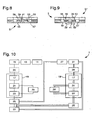
figure 10 est un schéma fonctionnel du procédé de fabrication selon l'invention ; - la
figure 11 est une représentation en perspective d'un rouage obtenu selon le procédé de l'invention ; - la
figure 12 est une représentation vue de dessus d'une aiguille obtenue selon l'invention ;
- the
Figures 1 to 7 are sections of a composite micromechanical part at different phases of the manufacturing method according to the invention; - the
figure 1b is a representation of thefigure 1 in perspective. - the
figure 8 is a representation of a first example of a final step according to the method of the invention; - the
figure 9 is a representation of a second example of a final step according to the method of the invention; - the
figure 10 is a block diagram of the manufacturing method according to the invention; - the
figure 11 is a perspective representation of a gear train obtained according to the method of the invention; - the
figure 12 is a view from above of a needle obtained according to the invention;
L'invention se rapporte à un procédé de fabrication 1 d'une pièce de micromécanique composite 51 silicium - métal. Comme visible aux
La première étape 11 consiste à se munir d'un substrat 3 du type « silicium sur isolant », très connu sous l'acronyme anglais « SOI ». Le substrat 3 comporte une couche supérieure 5 et une couche inférieure 7 composées de silicium mono ou polycristallin. Entre les couches supérieure 5 et inférieure 7 s'étend une couche intermédiaire 9 composée d'oxyde de silicium du type amorphe (SiO2).The
Préférentiellement dans cette étape 11, le substrat 3 est choisi afin que, comme visible à la
Dans une deuxième étape 13, comme visible aux
Dans l'exemple illustré à la
Dans une troisième étape 15, un gravage par attaque chimique humide ou sèche est réalisée pour prolonger, dans la couche intermédiaire 9, les cavités 37 et 45 afin que la partie 53 soit formée selon le même motif dans la couche intermédiaire 9 jusqu'à découvrir partiellement la couche inférieure 7.In a
Le procédé 1 selon l'invention comporte ensuite la mise en oeuvre d'un processus 19 du type LIGA (acronyme très connu provenant de l'allemand « Röntgenlithographie, Galvanoformung & Abformung ») comportant une succession d'étapes (17, 21 & 23) permettant d'électrodéposer selon une forme particulière un métal sur la face supérieure du substrat 3 à l'aide d'une résine photostructurée.The method 1 according to the invention then comprises the implementation of a
Dans une quatrième étape 17, on dépose, sur la face supérieure du substrat 3, une couche de résine photosensible 57 comme visible à la
Dans une cinquième étape 21, on réalise une photolithographie, c'est-à-dire qu'on expose sélectivement à un rayonnement R, au moyen par exemple d'un masque M partiellement ajouré comme visible à la
Dans l'exemple de la
Préférentiellement dans une sixième étape 29, on dépose sur la face supérieure du substrat 3 une couche 61 d'accrochage conductrice comme visible à la
Dans une septième étape 23, on réalise par électrodéposition le départ d'une couche métallique sur la face supérieure du substrat 3, c'est-à-dire que l'on fait croître un couche 63 métallique afin de former au moins une partie métallique 41 de la pièce de micromécanique 51. Dans l'exemple illustré à la
La présence du cylindre 75 de résine photostructurée oblige la croissance de la couche métallique 63 à se former par couches annulaires successives entre le cylindre 75 et la couche intermédiaire 9 puis entre le cylindre 75 et la couche supérieure 5 du substrat 3. Cette première phase d'électrodéposition permet de former une première partie 41 métallique dans au moins une portion de la cavité 45.The presence of the
On comprend donc à cette première phase de l'étape 23 que la pièce de micromécanique 51 est désormais formée sur une couche qui comporte une partie 53 en silicium et en oxyde de silicium dont au moins une portion d'une des cavités 45 comporte une partie 41 métallique.It is thus clear in this first phase of
Dans l'exemple illustré à la
Préférentiellement, la couche 63, c'est-à-dire notamment les parties métalliques 39 et 41 comporte du nickel, c'est-à-dire du nickel pur ou un de ses alliages. Préférentiellement, la différence de potentiel du substrat 3 nécessaire à l'étape 23 d'électrodéposition est réalisée par contact sur sa face inférieure et/ou supérieure.Preferably, the
Dans une huitième étape 25, un usinage de la face supérieure du substrat 3 est réalisée, par exemple par rodage, afin de niveler la hauteur de la partie métallique 39, obtenue lors ladite deuxième phase de l'étape 23, par rapport à l'épaisseur de l'anneau supérieur 73 et du cylindre 75 en la résine photostructurée comme visible à la
On comprend donc à cette étape 25 que la pièce de micromécanique 51 est désormais formée sur deux couches. La première couche comporte une partie 53 en silicium et en oxyde de silicium dont au moins une portion d'une des cavités 45 comporte une partie 41 métallique. La deuxième couche formée au-dessus de la première est formée par une deuxième partie 39 métallique.It is therefore understood at this
Dans des neuvième et dixième étapes 27 & 31, comme illustré par les doubles traits à la
Dans l'exemple illustré à la
Les étapes 27 et 31 n'ont pas une consécutivité préférée, de sorte que l'une peut être initiée avant l'autre et inversement. Préférentiellement, l'étape 27 d'usinage peut consister en un polissage mécano-chimique comme un rodage par abrasion chimique.
On comprend donc que, après ces étapes 27 & 31, la pièce de micromécanique 51 est désormais formée sur trois couches. La première couche comporte une partie 53 en silicium et en oxyde de silicium dont au moins une portion d'une des cavités 45 comporte une partie 41 métallique. La deuxième couche au-dessus de la première est formée par une deuxième partie 39 métallique. La troisième couche en dessous de la première est formée par une deuxième partie 65 en silicium.It is therefore understood that after these
Le procédé 1 selon l'invention comporte ensuite, comme illustré par les triples traits à la
Dans une onzième étape 17', on dépose sur la face inférieure du substrat 3 une couche de résine photosensible, par exemple à l'aide d'un procédé du type coulée par moule. Dans une douzième étape 21', on réalise une photolithographie permettant de réaliser le motif de la croissance de la future électrodéposition métallique.In an eleventh step 17 ', a layer of photoresist is deposited on the underside of the
Préférentiellement dans une treizième étape 29', on dépose sur la face inférieure du substrat 3 une couche d'accrochage. Cette étape peut être réalisée, par exemple, par dépôt sous vide, comme mentionné ci-dessus, d'une couche d'or pur ou un de ses alliages.Preferably in a thirteenth step 29 'is deposited on the underside of the substrate 3 a bonding layer. This step can be carried out, for example, by vacuum deposition, as mentioned above, of a layer of pure gold or one of its alloys.
Dans une quatorzième étape 23', on réalise par électrodéposition une couche métallique sur la face inférieure du substrat 3 afin de former au moins une partie supplémentaire métallique 41' de la pièce de micromécanique 51 dans au moins une portion de la cavité 47.In a fourteenth step 23 ', a metal layer is electroplated on the underside of the
On comprend donc à cette étape que la pièce de micromécanique 51 est toujours formée sur trois couches. La première couche comporte une partie 53 en silicium et en oxyde de silicium dont au moins une portion d'une des cavités 45 comporte une partie 41 métallique. La deuxième couche au-dessus de la première est formée par une deuxième partie 39 métallique. La troisième couche en dessous de la première est formée par une deuxième partie 65 en silicium dont au moins une portion d'une des cavités 47 comporte une partie supplémentaire 41' métallique.It is therefore understood at this stage that the
L'étape 23' d'électrodéposition peut être continuée afin de former des couches non plus dans la cavité 47 mais en dessous et, éventuellement, sur une partie de la couche inférieure 7 du substrat 3. Les couches successives sont alors formées exclusivement entre la résine, photostructurée lors de l'étape 21', en une deuxième partie supplémentaire 39' métallique.The electroplating step 23 'can be continued to form layers no longer in the
Préférentiellement, la couche métallique électrodéposée, c'est-à-dire notamment les parties métalliques supplémentaires 39' et 41' comporte du nickel, c'est-à-dire du nickel pur ou un de ses alliages.Preferably, the electrodeposited metal layer, that is to say in particular the additional metal parts 39 'and 41' comprises nickel, that is to say pure nickel or one of its alloys.
Dans une quinzième étape 25', un usinage de la face inférieure du substrat 3 est réalisée, par exemple par rodage, afin de correctement délimiter la deuxième partie supplémentaire métallique 39'. De manière similaire à la deuxième partie 39, la deuxième partie supplémentaire 39' métallique peut également comporter une denture 59'.In a fifteenth step 25 ', a machining of the underside of the
On comprend donc à cette étape que la pièce de micromécanique 51 est désormais formée sur quatre couches. La première couche comporte une partie 53 en silicium & en oxyde de silicium dont au moins une portion d'une des cavités 45 comporte une partie 41 métallique. La deuxième couche au-dessus de la première est formée par une deuxième partie 39 métallique. La troisième couche en dessous de la première est formée par une deuxième partie 65 en silicium dont au moins une portion d'une des cavités 47 comporte une partie supplémentaire 41' métallique. La quatrième couche en dessous de la troisième est formée par une deuxième partie supplémentaire 39' métallique.It is therefore understood at this stage that the
Bien entendu, l'intérêt d'un tel procédé est aussi de permettre, avantageusement, la réalisation de plusieurs pièces de micromécanique 51 sur un même substrat 3. De plus, à l'aide de l'explication ci-dessus et des traits simple, double et triple de la
Dans un premier mode de réalisation, l'étape de libération 33 du procédé 1 est réalisée après l'étape 25 de construction de la partie métallique 41 dans la partie 53 en silicium comme visualisé par les simples traits à la
Dans un deuxième mode de réalisation illustré à la
La pièce de micromécanique 51 obtenue selon ledit deuxième mode de réalisation du procédé 1 expliqué ci-dessus et en relation avec les
Dans un troisième mode de réalisation illustré à la
La pièce de micromécanique 51' comporte ainsi, comme visible à la
La pièce de micromécanique 51' obtenue selon ledit troisième mode de réalisation du procédé 1 expliqué ci-dessus et en relation avec les
Dans tous ces modes de réalisation, les pièces de micromécanique 51, 51', 51" sont avantageusement chassées non pas directement sur une partie 53 & 65 en silicium mais sur les parties métalliques 39, 39', 41 et 41'. Préférentiellement afin que, notamment, la partie métallique 41 isole suffisamment la partie 53 en silicium, l'épaisseur est supérieure à 6 microns. En effet, au-delà de cette épaisseur et idéalement à partir de 10 microns, un métal comme par exemple le nickel est capable d'absorber élastiquement ou plastiquement les efforts sans les restituer au silicium.In all these embodiments, the pieces of
Il faut comprendre à la lecture de l'explication ci-dessus que les pièces de micromécanique 51, 51', 51" des figures ne sont que des exemples de réalisation qui montre que le procédé 1 permet de réaliser un empilement jusqu'à quatre couches (deux comportant du métal et deux comportant du silicium et du métal) sans complications excessives. La configuration du premier mode de réalisation pourrait ainsi constituer la plus simple des pièces de micromécanique et, celle du troisième mode de réalisation, une complication haute.It should be understood from the reading of the above explanation that the
Dans une variante visualisé en traits interrompus courts à la
Bien entendu, la présente invention ne se limite pas à l'exemple illustré mais est susceptible de diverses variantes et modifications qui apparaîtront à l'homme de l'art. En particulier, d'autres couches 63 métalliques peuvent être envisagées comme par exemple de l'or, de l'aluminium, du chrome ou un de leur alliages. De même, d'autres couches d'accrochage 61 peuvent être envisagées si elles sont conductrices et qu'elles adhèrent parfaitement au métal choisi pour la couche 63 de croissance galvanique. Cependant, il est à noter que l'étape 29 de dépôt de la couche 61 n'est pas essentielle au bon déroulement de la croissance galvanique si les deux couches en silicium 5 et 7 sont dopées.Of course, the present invention is not limited to the illustrated example but is susceptible of various variations and modifications that will occur to those skilled in the art. In particular, other
De même d'autres motifs que les dentures 55, 59, 59' & 67 peuvent être gravés comme des crochets ou des cliquets. Il est également à noter que la couche 63 peut être réalisée contre lesdits motifs gravés tels que les dentures 55, 59, 59' & 67 par exemple.Similarly other reasons that the
De même, la photolithographie peut, bien sûr, former une structure en négatif ou en positif suivant la résine photosensible employée ou l'application prévue. Le dépôt de la couche de résine 57 peut également être envisagé d'être réalisé par un processus connu sous le terme anglais de « spray coating ».Similarly, photolithography can, of course, form a negative or positive structure depending on the photoresist used or the intended application. The deposition of the
Enfin, la couche 63 métallique peut être réalisée aussi bien sur une portion de paroi intérieure d'une cavité 45 que sur la paroi périphérique d'au moins une des parties en silicium 53 et 65. La couche 63 peut également être structurée afin qu'elle soit reliée à ladite paroi en silicium par l'intermédiaire de ponts de matière.Finally, the
Claims (13)
- Method of manufacturing (1) a silicon-metal composite micromechanical component (51, 51', 51") including the following steps:a) taking (11) a substrate (3) including a top (5) and bottom (7) silicon layer between which an intermediate silicon oxide layer (9) extends,b) selectively etching (13) at least one cavity (37, 45, 45") in the top layer (5) to define the pattern of a silicon part (53, 53") of said component;c) continuing the etch (15) of said at least one cavity (37, 45, 45") in the intermediate layer (9);characterized in that it further includes the following steps:d) growing (17, 21, 23) a metal layer (63) at least from one portion of said at least one cavity (37, 45, 45") in order to form a metal part (41, 41', 41") in the thickness of said component in order to insulate the silicon part (53, 53") of said micromechanical component from destructive stress;e) releasing (33) the silicon-metal composite micromechanical component (51, 51', 51") from the substrate (3).
- Method (1) according to claim 1, characterized in that step d) includes the following steps:- covering (17) the top of the substrate (3) with photosensitive resin (57);- selectively performing (21) photolithography on the photosensitive resin (57) to photostructure (71, 73, 75) said resin in accordance with the predetermined pattern of the metal part (39, 41);- depositing (23) a metal layer by electroplating, starting from the top conductive surface of the bottom layer (7), which is vertical to said at least one cavity (37, 45, 45") by growing, from the bottom, the layer (63) between respectively the photostructured resin (75) and the intermediate (9) or top (5) layer for forming the metal part (41, 41', 41") in accordance with said pattern; and in that step e) is performed by removing (33) the photostructured resin (71, 73, 75).
- Method (1) according to claim 2, characterized in that said top conductive surface of the bottom layer (7), which is vertical to said at least once cavity (37, 45, 45") is made conductive by doping the bottom layer (7) and/or by the deposition (29) of a conductive layer (61).
- Method (1) according to claim 2 or 3, characterized in that, during photolithography step (21), the photostructured resin (71, 73, 75) projects (73, 75) from the top layer (5) of the substrate (3) so that the layer (63) can continue to grow by electroplating (23) at least between said projecting portions of the photostructured resin (73, 75) in order to form a second metal part (39) of the micromechanical component (51, 51') above the silicon part (53).
- Method (1) according to any of the preceding claims, characterized in that, after step d), it includes a step (25) of machining the top surface of the substrate (3) so as to level the metal layer (63) to the same height as the top end of said photostructured resin (73, 75).
- Method (1) according to any of the preceding claims, characterized in that the metal layer (63, 39, 39', 41, 41', 41") includes nickel.
- Method (1) according to any of the preceding claims, characterized in that, before the release step (33), it includes steps of machining (27) and etching (31) at least one cavity (47, 49) in the bottom layer (7) of the substrate (3) to form a second silicon part (65) in the micromechanical component (51, 51') in accordance with a determined shape and thickness.
- Method (1) according to claim 7, characterized in that, between the steps of machining and etching (27, 31) the bottom layer (7) of the substrate (3), it includes a release step (33), a step (17', 21', 23') of growing a second metal layer (41') by electroplating in at least one portion of said at least one cavity (47) of the bottom layer (7) so as to form at least one additional metal part (41') in the thickness of the bottom layer (7).
- Method (1) according to claim 8, characterized in that the growth step includes the following steps:- covering (17') the bottom of the substrate (3) with photosensitive resin;- selectively (21') performing photolithography on the photosensitive resin in order to photostructure said resin in accordance with the predetermined pattern of the metal part (41');- depositing (23') a metal layer by electroplating starting from the bottom of said at least one cavity (47), by growing therein, from the bottom, the layer for forming the metal part (41') in accordance with said pattern.
- Method (1) according to claim 9, characterized in that, during the photolithography step (21'), the photostructured resin projects from the bottom layer (7) of the substrate (3) so that the layer can continue to grow by electroplating (23') in order to form a second additional metal part (39') of the micromechanical component (51') below the second silicon part (65).
- Method (1) according to any of the preceding claims, characterized in that, before the release step (33), it includes a step (25') of machining the bottom surface of the substrate (3) in order to level the metal part (39') to the same height as the bottom end of said photostructured resin.
- Method (1) according to any of claims 8 to 11, characterized in that the second electroplated metal layer (39', 41') includes nickel.
- Method (1) according to any of the preceding claims, characterized in that several micromechanical components (51, 51', 51") are manufactured in the same substrate (3).
Priority Applications (1)
| Application Number | Priority Date | Filing Date | Title |
|---|---|---|---|
| EP08848955.4A EP2259997B2 (en) | 2007-11-16 | 2008-11-12 | Method for manufacturing a composite silicon-metal micromechanical component |
Applications Claiming Priority (3)
| Application Number | Priority Date | Filing Date | Title |
|---|---|---|---|
| EP07120883A EP2060534A1 (en) | 2007-11-16 | 2007-11-16 | Composite silicon-metal micromechanical component and method for manufacturing same |
| PCT/EP2008/065347 WO2009062943A1 (en) | 2007-11-16 | 2008-11-12 | Silicon-metal composite micromechanical part and method for producing same |
| EP08848955.4A EP2259997B2 (en) | 2007-11-16 | 2008-11-12 | Method for manufacturing a composite silicon-metal micromechanical component |
Publications (3)
| Publication Number | Publication Date |
|---|---|
| EP2259997A1 EP2259997A1 (en) | 2010-12-15 |
| EP2259997B1 EP2259997B1 (en) | 2011-06-01 |
| EP2259997B2 true EP2259997B2 (en) | 2015-09-30 |
Family
ID=39420509
Family Applications (2)
| Application Number | Title | Priority Date | Filing Date |
|---|---|---|---|
| EP07120883A Withdrawn EP2060534A1 (en) | 2007-11-16 | 2007-11-16 | Composite silicon-metal micromechanical component and method for manufacturing same |
| EP08848955.4A Active EP2259997B2 (en) | 2007-11-16 | 2008-11-12 | Method for manufacturing a composite silicon-metal micromechanical component |
Family Applications Before (1)
| Application Number | Title | Priority Date | Filing Date |
|---|---|---|---|
| EP07120883A Withdrawn EP2060534A1 (en) | 2007-11-16 | 2007-11-16 | Composite silicon-metal micromechanical component and method for manufacturing same |
Country Status (10)
| Country | Link |
|---|---|
| US (2) | US8486279B2 (en) |
| EP (2) | EP2060534A1 (en) |
| JP (1) | JP5478498B2 (en) |
| KR (1) | KR20100084527A (en) |
| CN (1) | CN101861281B (en) |
| AT (1) | ATE511494T1 (en) |
| HK (1) | HK1144190A1 (en) |
| RU (1) | RU2474532C2 (en) |
| TW (1) | TWI436939B (en) |
| WO (1) | WO2009062943A1 (en) |
Families Citing this family (28)
| Publication number | Priority date | Publication date | Assignee | Title |
|---|---|---|---|---|
| EP2230206B1 (en) | 2009-03-13 | 2013-07-17 | Nivarox-FAR S.A. | Electroplating mould and method for manufacturing same |
| EP2230207A1 (en) | 2009-03-13 | 2010-09-22 | Nivarox-FAR S.A. | Electroplating mould and method for manufacturing the same |
| EP2263971A1 (en) | 2009-06-09 | 2010-12-22 | Nivarox-FAR S.A. | Composite micromechanical part and method for manufacturing same |
| EP2309342A1 (en) * | 2009-10-07 | 2011-04-13 | Nivarox-FAR S.A. | Loose-mounted wheel made from a micro-machinable material, and manufacturing method |
| CH702156B1 (en) * | 2009-11-13 | 2017-08-31 | Nivarox Far Sa | Spiral balance resonator for a timepiece. |
| DE102010004269B4 (en) | 2010-01-09 | 2018-06-28 | Micromotion Gmbh | Gear pairing and gearbox, in particular eccentric gear, planetary gear or stress wave gear |
| EP2405300A1 (en) * | 2010-07-09 | 2012-01-11 | Mimotec S.A. | Manufacturing method for multi-level metal parts through an LIGA type method and parts obtained using the method |
| EP2484629B1 (en) * | 2011-02-03 | 2013-06-26 | Nivarox-FAR S.A. | Perforated complex micromechanical part |
| EP2484628A1 (en) * | 2011-02-03 | 2012-08-08 | Nivarox-FAR S.A. | Micromechanical item having low surface roughness |
| CN102167282A (en) * | 2011-04-07 | 2011-08-31 | 天津海鸥表业集团有限公司 | Method for processing microstructure of silicon and metal composite material |
| CH705228A1 (en) * | 2011-07-06 | 2013-01-15 | Suisse Electronique Microtech | Mechanical piece composite silicon metal and its production process. |
| EP2579104B1 (en) * | 2011-10-07 | 2014-06-25 | CSEM Centre Suisse d'Electronique et de Microtechnique SA - Recherche et Développement | Method for manufacturing a composite timepiece |
| CH705724B9 (en) | 2011-11-03 | 2016-05-13 | Sigatec Sa | micromechanical component, in particular for watches. |
| JP6345493B2 (en) * | 2014-02-25 | 2018-06-20 | シチズン時計株式会社 | Hairspring |
| EP2937311B1 (en) * | 2014-04-25 | 2019-08-21 | Rolex Sa | Method for manufacturing a reinforced timepiece component, corresponding timepiece component and timepiece |
| CH709729A2 (en) * | 2014-06-03 | 2015-12-15 | Swatch Group Res & Dev Ltd | lining part based photostructurable glass. |
| EP2952979B1 (en) * | 2014-06-03 | 2017-03-01 | Nivarox-FAR S.A. | Timepiece component made of photostructurable glass |
| CH710107B1 (en) * | 2014-09-09 | 2019-06-14 | Seiko Instr Lnc | Mechanical component, movement, timepiece and method of manufacturing the mechanical component. |
| EP3232277B1 (en) | 2014-12-12 | 2021-04-21 | Citizen Watch Co., Ltd. | Timepiece component and method for manufacturing timepiece component |
| EP3034461B1 (en) | 2014-12-19 | 2020-07-01 | Rolex Sa | Production of a multi-level clock component |
| EP3035125B1 (en) * | 2014-12-19 | 2018-01-10 | Rolex Sa | Method for manufacturing a multi-level clock component |
| EP3181515A1 (en) | 2015-12-15 | 2017-06-21 | CSEM Centre Suisse d'Electronique et de Microtechnique SA - Recherche et Développement | Composite timepiece and method for manufacturing same |
| EP3202708B1 (en) * | 2016-02-03 | 2023-05-03 | Rolex Sa | Method for manufacturing a hybrid clock component |
| CH712210B1 (en) * | 2016-03-14 | 2020-02-14 | Nivarox Sa | Method of manufacturing a clock display component. |
| EP3249474B1 (en) * | 2016-05-26 | 2019-03-13 | ETA SA Manufacture Horlogère Suisse | Analogue display hand |
| EP3266738B1 (en) * | 2016-07-06 | 2019-03-06 | The Swatch Group Research and Development Ltd. | Method for manufacturing a part for a timepiece provided with a multi-level exterior element |
| EP3764167A1 (en) * | 2019-07-10 | 2021-01-13 | Patek Philippe SA Genève | Method for obtaining a timepiece component in which the surface is at least partially covered with a coloured layer |
| EP3839625A1 (en) * | 2019-12-18 | 2021-06-23 | Nivarox-FAR S.A. | Method for manufacturing a timepiece component and component produced by this method |
Family Cites Families (14)
| Publication number | Priority date | Publication date | Assignee | Title |
|---|---|---|---|---|
| RU2137249C1 (en) * | 1998-03-31 | 1999-09-10 | Санкт-Петербургский государственный электротехнический университет | Process of manufacture of micromechanical instruments |
| DE19817311B4 (en) * | 1998-04-18 | 2007-03-22 | Robert Bosch Gmbh | Manufacturing method for micromechanical component |
| US6887391B1 (en) * | 2000-03-24 | 2005-05-03 | Analog Devices, Inc. | Fabrication and controlled release of structures using etch-stop trenches |
| DE10055421A1 (en) * | 2000-11-09 | 2002-05-29 | Bosch Gmbh Robert | Method for producing a micromechanical structure and micromechanical structure |
| US6506620B1 (en) * | 2000-11-27 | 2003-01-14 | Microscan Systems Incorporated | Process for manufacturing micromechanical and microoptomechanical structures with backside metalization |
| FR2852111B1 (en) * | 2003-03-05 | 2005-06-24 | Univ Franche Comte | CLOCK DEVICE USING MEMS TECHNOLOGY |
| JP2006064575A (en) * | 2004-08-27 | 2006-03-09 | Seiko Epson Corp | Components of watch, sub-assembly of watch, and watch |
| US7204737B2 (en) * | 2004-09-23 | 2007-04-17 | Temic Automotive Of North America, Inc. | Hermetically sealed microdevice with getter shield |
| CH696475A5 (en) * | 2005-05-12 | 2007-06-29 | Eta Sa Mft Horlogere Suisse | Body analog display crystalline material, timepiece provided with such a display element and method for its manufacture. |
| EP1780612A1 (en) * | 2005-10-25 | 2007-05-02 | ETA SA Manufacture Horlogère Suisse | Vorrichtung zur analogen Anzeige, die eine Planetengetriebe aufweist |
| TWI276805B (en) * | 2005-11-10 | 2007-03-21 | Mjc Probe Inc | Probe of probe card and manufacturing method thereof |
| ES2327350T3 (en) * | 2006-04-07 | 2009-10-28 | Eta Sa Manufacture Horlogere Suisse | INVESTING MECHANISM FOR UNIDIRECTIONAL ROTARY DRIVING OF A MOBILE. |
| JP5231769B2 (en) * | 2007-02-27 | 2013-07-10 | セイコーインスツル株式会社 | ELECTROMOLD, ELECTROMOLD MANUFACTURING METHOD, WATCH PARTS, AND WATCH |
| CH714952B1 (en) * | 2007-05-08 | 2019-10-31 | Patek Philippe Sa Geneve | Watchmaking component, its method of manufacture and application of this method. |
-
2007
- 2007-11-16 EP EP07120883A patent/EP2060534A1/en not_active Withdrawn
-
2008
- 2008-11-12 RU RU2010124426/28A patent/RU2474532C2/en active
- 2008-11-12 WO PCT/EP2008/065347 patent/WO2009062943A1/en active Application Filing
- 2008-11-12 JP JP2010533559A patent/JP5478498B2/en active Active
- 2008-11-12 KR KR1020107009432A patent/KR20100084527A/en not_active Application Discontinuation
- 2008-11-12 EP EP08848955.4A patent/EP2259997B2/en active Active
- 2008-11-12 US US12/743,210 patent/US8486279B2/en active Active
- 2008-11-12 CN CN2008801161499A patent/CN101861281B/en active Active
- 2008-11-12 AT AT08848955T patent/ATE511494T1/en not_active IP Right Cessation
- 2008-11-14 TW TW097144155A patent/TWI436939B/en not_active IP Right Cessation
-
2010
- 2010-11-19 HK HK10110805.2A patent/HK1144190A1/en unknown
-
2013
- 2013-06-14 US US13/917,975 patent/US20130279307A1/en not_active Abandoned
Non-Patent Citations (1)
| Title |
|---|
| MARC-ANDRÉ GLASSEY: "Sigatec SA: a start-up company for Silicon Microparts", SWISS CONFEDERATION - STATE SECRETARIAT FOR EDUCATION, RESEARCH AND INNOVATION SERI, 15 November 2007 (2007-11-15), pages 1 - 39, XP055186088, Retrieved from the Internet <URL:http://www.sbfi.admin.ch/kti/aktuell/00545/00598/index.html?lang=en&print_style=yes> [retrieved on 20150427] † |
Also Published As
| Publication number | Publication date |
|---|---|
| RU2010124426A (en) | 2011-12-27 |
| EP2060534A1 (en) | 2009-05-20 |
| TWI436939B (en) | 2014-05-11 |
| CN101861281A (en) | 2010-10-13 |
| ATE511494T1 (en) | 2011-06-15 |
| EP2259997A1 (en) | 2010-12-15 |
| RU2474532C2 (en) | 2013-02-10 |
| KR20100084527A (en) | 2010-07-26 |
| HK1144190A1 (en) | 2011-02-02 |
| JP2011514846A (en) | 2011-05-12 |
| US20130279307A1 (en) | 2013-10-24 |
| TW200927640A (en) | 2009-07-01 |
| CN101861281B (en) | 2012-11-21 |
| US20100243603A1 (en) | 2010-09-30 |
| EP2259997B1 (en) | 2011-06-01 |
| US8486279B2 (en) | 2013-07-16 |
| JP5478498B2 (en) | 2014-04-23 |
| WO2009062943A1 (en) | 2009-05-22 |
Similar Documents
| Publication | Publication Date | Title |
|---|---|---|
| EP2259997B2 (en) | Method for manufacturing a composite silicon-metal micromechanical component | |
| EP2105807B1 (en) | Monobloc elevated curve spiral and method for manufacturing same | |
| EP2261171B1 (en) | Method for manufacturing a composite micromechanical part | |
| EP2257856B1 (en) | Integral adjusting member and method for making same | |
| EP2230208B1 (en) | Electroplating mould and method for manufacturing the same | |
| EP2104006B1 (en) | Single-body double spiral and method for manufacturing same | |
| EP2230206B1 (en) | Electroplating mould and method for manufacturing same | |
| WO2009115470A1 (en) | Integral hairspring made of a silicon-based material and method for making same | |
| EP3066044B1 (en) | Hollow micromechanical part which has a plurality of functional levels and is unitary made of a material comprising a synthetic carbon allotrope | |
| EP2154582A1 (en) | Gear method for a clock piece | |
| CH705433B1 (en) | Manufacturing micromechanics composite silicon-metal part useful in clock element, comprises manufacturing substrate with upper and lower layers, and selectively etching cavity in upper layer to define pattern in portion of silicon part | |
| EP2309341B1 (en) | Manufacturing method of a loose-mounted wheel made from a micro-machinable material | |
| WO2012104110A1 (en) | Method for producing a complex smooth micromechanical part | |
| CH701266A2 (en) | Composite micromechanical piece e.g. escape wheel, fabrication method for timepiece, involves realizing electroplating process by connecting electrode to lower layer to form metallic parts of micromechanical piece released from substrate | |
| EP3839659B1 (en) | Method for decorating a mechanical part | |
| EP3412625A1 (en) | Method for manufacturing a micromechanical part | |
| CH706252B1 (en) | Method for manufacturing integral single-piece spiral of clock element, involves selectively engraving cavity in additional layer to define portion for spiral spring made of material containing silicon, and releasing spiral of substrate | |
| CH700554A2 (en) | Manufacturing a mold, comprises supplying substrate comprising upper layer and lower layer, etching pattern in upper layer up to intermediate layer, and overlaying upper part of substrate with electrically insulating coating | |
| EP4312085A1 (en) | Method for manufacturing a clock component | |
| CH701972A2 (en) | Method for manufacturing wheel of clock element in clock industry, involves forming unit in lower layer for forming another cavity of another wheel to structure photo resist resin at side of lower layer that forms liner at walls of cavity | |
| CH713854A2 (en) | Method of manufacturing a micromechanical part | |
| CH700553A2 (en) | Manufacturing a mold, comprises depositing electrically conductive layer on top and bottom of plate, soldering plate with substrate using adhesive layer, removing part of top conductive layer from plate, and etching the plate | |
| CH707297B1 (en) | Single-piece regulating element for timepiece, has balancer cooperating with spiral having hairspring mounted coaxially on ferrule, where axial extension portion of ferrule is connected to balancer as single-piece |
Legal Events
| Date | Code | Title | Description |
|---|---|---|---|
| PUAI | Public reference made under article 153(3) epc to a published international application that has entered the european phase |
Free format text: ORIGINAL CODE: 0009012 |
|
| 17P | Request for examination filed |
Effective date: 20101005 |
|
| AK | Designated contracting states |
Kind code of ref document: A1 Designated state(s): AT BE BG CH CY CZ DE DK EE ES FI FR GB GR HR HU IE IS IT LI LT LU LV MC MT NL NO PL PT RO SE SI SK TR |
|
| AX | Request for extension of the european patent |
Extension state: AL BA MK RS |
|
| GRAP | Despatch of communication of intention to grant a patent |
Free format text: ORIGINAL CODE: EPIDOSNIGR1 |
|
| DAX | Request for extension of the european patent (deleted) | ||
| REG | Reference to a national code |
Ref country code: DE Ref legal event code: R079 Ref document number: 602008007376 Country of ref document: DE Free format text: PREVIOUS MAIN CLASS: B81C0005000000 Ipc: B81C0099000000 |
|
| RIC1 | Information provided on ipc code assigned before grant |
Ipc: B81C 99/00 20100101AFI20110307BHEP Ipc: C25D 1/00 20060101ALI20110307BHEP Ipc: G04B 13/00 20060101ALI20110307BHEP |
|
| GRAS | Grant fee paid |
Free format text: ORIGINAL CODE: EPIDOSNIGR3 |
|
| GRAA | (expected) grant |
Free format text: ORIGINAL CODE: 0009210 |
|
| AK | Designated contracting states |
Kind code of ref document: B1 Designated state(s): AT BE BG CH CY CZ DE DK EE ES FI FR GB GR HR HU IE IS IT LI LT LU LV MC MT NL NO PL PT RO SE SI SK TR |
|
| REG | Reference to a national code |
Ref country code: GB Ref legal event code: FG4D Free format text: NOT ENGLISH |
|
| REG | Reference to a national code |
Ref country code: CH Ref legal event code: EP |
|
| REG | Reference to a national code |
Ref country code: IE Ref legal event code: FG4D Free format text: LANGUAGE OF EP DOCUMENT: FRENCH |
|
| REG | Reference to a national code |
Ref country code: CH Ref legal event code: NV Representative=s name: ICB INGENIEURS CONSEILS EN BREVETS SA |
|
| REG | Reference to a national code |
Ref country code: DE Ref legal event code: R096 Ref document number: 602008007376 Country of ref document: DE Effective date: 20110714 |
|
| REG | Reference to a national code |
Ref country code: NL Ref legal event code: VDEP Effective date: 20110601 |
|
| PG25 | Lapsed in a contracting state [announced via postgrant information from national office to epo] |
Ref country code: HR Free format text: LAPSE BECAUSE OF FAILURE TO SUBMIT A TRANSLATION OF THE DESCRIPTION OR TO PAY THE FEE WITHIN THE PRESCRIBED TIME-LIMIT Effective date: 20110601 Ref country code: SE Free format text: LAPSE BECAUSE OF FAILURE TO SUBMIT A TRANSLATION OF THE DESCRIPTION OR TO PAY THE FEE WITHIN THE PRESCRIBED TIME-LIMIT Effective date: 20110601 Ref country code: LT Free format text: LAPSE BECAUSE OF FAILURE TO SUBMIT A TRANSLATION OF THE DESCRIPTION OR TO PAY THE FEE WITHIN THE PRESCRIBED TIME-LIMIT Effective date: 20110601 Ref country code: NO Free format text: LAPSE BECAUSE OF FAILURE TO SUBMIT A TRANSLATION OF THE DESCRIPTION OR TO PAY THE FEE WITHIN THE PRESCRIBED TIME-LIMIT Effective date: 20110901 |
|
| PG25 | Lapsed in a contracting state [announced via postgrant information from national office to epo] |
Ref country code: LV Free format text: LAPSE BECAUSE OF FAILURE TO SUBMIT A TRANSLATION OF THE DESCRIPTION OR TO PAY THE FEE WITHIN THE PRESCRIBED TIME-LIMIT Effective date: 20110601 Ref country code: AT Free format text: LAPSE BECAUSE OF FAILURE TO SUBMIT A TRANSLATION OF THE DESCRIPTION OR TO PAY THE FEE WITHIN THE PRESCRIBED TIME-LIMIT Effective date: 20110601 Ref country code: CY Free format text: LAPSE BECAUSE OF FAILURE TO SUBMIT A TRANSLATION OF THE DESCRIPTION OR TO PAY THE FEE WITHIN THE PRESCRIBED TIME-LIMIT Effective date: 20110601 Ref country code: ES Free format text: LAPSE BECAUSE OF FAILURE TO SUBMIT A TRANSLATION OF THE DESCRIPTION OR TO PAY THE FEE WITHIN THE PRESCRIBED TIME-LIMIT Effective date: 20110912 Ref country code: FI Free format text: LAPSE BECAUSE OF FAILURE TO SUBMIT A TRANSLATION OF THE DESCRIPTION OR TO PAY THE FEE WITHIN THE PRESCRIBED TIME-LIMIT Effective date: 20110601 Ref country code: SI Free format text: LAPSE BECAUSE OF FAILURE TO SUBMIT A TRANSLATION OF THE DESCRIPTION OR TO PAY THE FEE WITHIN THE PRESCRIBED TIME-LIMIT Effective date: 20110601 Ref country code: GR Free format text: LAPSE BECAUSE OF FAILURE TO SUBMIT A TRANSLATION OF THE DESCRIPTION OR TO PAY THE FEE WITHIN THE PRESCRIBED TIME-LIMIT Effective date: 20110902 |
|
| REG | Reference to a national code |
Ref country code: IE Ref legal event code: FD4D |
|
| PG25 | Lapsed in a contracting state [announced via postgrant information from national office to epo] |
Ref country code: NL Free format text: LAPSE BECAUSE OF FAILURE TO SUBMIT A TRANSLATION OF THE DESCRIPTION OR TO PAY THE FEE WITHIN THE PRESCRIBED TIME-LIMIT Effective date: 20110601 |
|
| PG25 | Lapsed in a contracting state [announced via postgrant information from national office to epo] |
Ref country code: CZ Free format text: LAPSE BECAUSE OF FAILURE TO SUBMIT A TRANSLATION OF THE DESCRIPTION OR TO PAY THE FEE WITHIN THE PRESCRIBED TIME-LIMIT Effective date: 20110601 Ref country code: EE Free format text: LAPSE BECAUSE OF FAILURE TO SUBMIT A TRANSLATION OF THE DESCRIPTION OR TO PAY THE FEE WITHIN THE PRESCRIBED TIME-LIMIT Effective date: 20110601 Ref country code: PT Free format text: LAPSE BECAUSE OF FAILURE TO SUBMIT A TRANSLATION OF THE DESCRIPTION OR TO PAY THE FEE WITHIN THE PRESCRIBED TIME-LIMIT Effective date: 20111003 Ref country code: IE Free format text: LAPSE BECAUSE OF FAILURE TO SUBMIT A TRANSLATION OF THE DESCRIPTION OR TO PAY THE FEE WITHIN THE PRESCRIBED TIME-LIMIT Effective date: 20110601 Ref country code: IS Free format text: LAPSE BECAUSE OF FAILURE TO SUBMIT A TRANSLATION OF THE DESCRIPTION OR TO PAY THE FEE WITHIN THE PRESCRIBED TIME-LIMIT Effective date: 20111001 |
|
| PG25 | Lapsed in a contracting state [announced via postgrant information from national office to epo] |
Ref country code: RO Free format text: LAPSE BECAUSE OF FAILURE TO SUBMIT A TRANSLATION OF THE DESCRIPTION OR TO PAY THE FEE WITHIN THE PRESCRIBED TIME-LIMIT Effective date: 20110601 Ref country code: PL Free format text: LAPSE BECAUSE OF FAILURE TO SUBMIT A TRANSLATION OF THE DESCRIPTION OR TO PAY THE FEE WITHIN THE PRESCRIBED TIME-LIMIT Effective date: 20110601 Ref country code: SK Free format text: LAPSE BECAUSE OF FAILURE TO SUBMIT A TRANSLATION OF THE DESCRIPTION OR TO PAY THE FEE WITHIN THE PRESCRIBED TIME-LIMIT Effective date: 20110601 |
|
| PLBI | Opposition filed |
Free format text: ORIGINAL CODE: 0009260 |
|
| PLAX | Notice of opposition and request to file observation + time limit sent |
Free format text: ORIGINAL CODE: EPIDOSNOBS2 |
|
| 26 | Opposition filed |
Opponent name: MIMOTEC S.A. Effective date: 20120224 |
|
| REG | Reference to a national code |
Ref country code: DE Ref legal event code: R026 Ref document number: 602008007376 Country of ref document: DE Effective date: 20120224 |
|
| BERE | Be: lapsed |
Owner name: NIVAROX-FAR S.A. Effective date: 20111130 |
|
| PG25 | Lapsed in a contracting state [announced via postgrant information from national office to epo] |
Ref country code: IT Free format text: LAPSE BECAUSE OF FAILURE TO SUBMIT A TRANSLATION OF THE DESCRIPTION OR TO PAY THE FEE WITHIN THE PRESCRIBED TIME-LIMIT Effective date: 20110601 |
|
| PG25 | Lapsed in a contracting state [announced via postgrant information from national office to epo] |
Ref country code: MC Free format text: LAPSE BECAUSE OF NON-PAYMENT OF DUE FEES Effective date: 20111130 Ref country code: DK Free format text: LAPSE BECAUSE OF FAILURE TO SUBMIT A TRANSLATION OF THE DESCRIPTION OR TO PAY THE FEE WITHIN THE PRESCRIBED TIME-LIMIT Effective date: 20110601 |
|
| PLBB | Reply of patent proprietor to notice(s) of opposition received |
Free format text: ORIGINAL CODE: EPIDOSNOBS3 |
|
| PG25 | Lapsed in a contracting state [announced via postgrant information from national office to epo] |
Ref country code: BE Free format text: LAPSE BECAUSE OF NON-PAYMENT OF DUE FEES Effective date: 20111130 |
|
| PG25 | Lapsed in a contracting state [announced via postgrant information from national office to epo] |
Ref country code: MT Free format text: LAPSE BECAUSE OF FAILURE TO SUBMIT A TRANSLATION OF THE DESCRIPTION OR TO PAY THE FEE WITHIN THE PRESCRIBED TIME-LIMIT Effective date: 20110601 |
|
| PG25 | Lapsed in a contracting state [announced via postgrant information from national office to epo] |
Ref country code: LU Free format text: LAPSE BECAUSE OF NON-PAYMENT OF DUE FEES Effective date: 20111112 |
|
| PG25 | Lapsed in a contracting state [announced via postgrant information from national office to epo] |
Ref country code: BG Free format text: LAPSE BECAUSE OF FAILURE TO SUBMIT A TRANSLATION OF THE DESCRIPTION OR TO PAY THE FEE WITHIN THE PRESCRIBED TIME-LIMIT Effective date: 20110901 |
|
| PG25 | Lapsed in a contracting state [announced via postgrant information from national office to epo] |
Ref country code: TR Free format text: LAPSE BECAUSE OF FAILURE TO SUBMIT A TRANSLATION OF THE DESCRIPTION OR TO PAY THE FEE WITHIN THE PRESCRIBED TIME-LIMIT Effective date: 20110601 |
|
| PG25 | Lapsed in a contracting state [announced via postgrant information from national office to epo] |
Ref country code: HU Free format text: LAPSE BECAUSE OF FAILURE TO SUBMIT A TRANSLATION OF THE DESCRIPTION OR TO PAY THE FEE WITHIN THE PRESCRIBED TIME-LIMIT Effective date: 20110601 |
|
| PUAH | Patent maintained in amended form |
Free format text: ORIGINAL CODE: 0009272 |
|
| STAA | Information on the status of an ep patent application or granted ep patent |
Free format text: STATUS: PATENT MAINTAINED AS AMENDED |
|
| 27A | Patent maintained in amended form |
Effective date: 20150930 |
|
| AK | Designated contracting states |
Kind code of ref document: B2 Designated state(s): AT BE BG CH CY CZ DE DK EE ES FI FR GB GR HR HU IE IS IT LI LT LU LV MC MT NL NO PL PT RO SE SI SK TR |
|
| REG | Reference to a national code |
Ref country code: CH Ref legal event code: AELC Ref country code: DE Ref legal event code: R102 Ref document number: 602008007376 Country of ref document: DE |
|
| REG | Reference to a national code |
Ref country code: FR Ref legal event code: PLFP Year of fee payment: 8 |
|
| REG | Reference to a national code |
Ref country code: FR Ref legal event code: PLFP Year of fee payment: 9 |
|
| PGFP | Annual fee paid to national office [announced via postgrant information from national office to epo] |
Ref country code: GB Payment date: 20161027 Year of fee payment: 9 |
|
| REG | Reference to a national code |
Ref country code: FR Ref legal event code: PLFP Year of fee payment: 10 |
|
| GBPC | Gb: european patent ceased through non-payment of renewal fee |
Effective date: 20171112 |
|
| REG | Reference to a national code |
Ref country code: FR Ref legal event code: PLFP Year of fee payment: 11 |
|
| PG25 | Lapsed in a contracting state [announced via postgrant information from national office to epo] |
Ref country code: GB Free format text: LAPSE BECAUSE OF NON-PAYMENT OF DUE FEES Effective date: 20171112 |
|
| P01 | Opt-out of the competence of the unified patent court (upc) registered |
Effective date: 20230611 |
|
| PGFP | Annual fee paid to national office [announced via postgrant information from national office to epo] |
Ref country code: FR Payment date: 20231020 Year of fee payment: 16 Ref country code: DE Payment date: 20231019 Year of fee payment: 16 Ref country code: CH Payment date: 20231202 Year of fee payment: 16 |