EP3266738B1 - Method for manufacturing a part for a timepiece provided with a multi-level exterior element - Google Patents
Method for manufacturing a part for a timepiece provided with a multi-level exterior element Download PDFInfo
- Publication number
- EP3266738B1 EP3266738B1 EP16178118.2A EP16178118A EP3266738B1 EP 3266738 B1 EP3266738 B1 EP 3266738B1 EP 16178118 A EP16178118 A EP 16178118A EP 3266738 B1 EP3266738 B1 EP 3266738B1
- Authority
- EP
- European Patent Office
- Prior art keywords
- layer
- orifice
- additional
- metal
- base
- Prior art date
- Legal status (The legal status is an assumption and is not a legal conclusion. Google has not performed a legal analysis and makes no representation as to the accuracy of the status listed.)
- Active
Links
- 238000000034 method Methods 0.000 title claims description 52
- 238000004519 manufacturing process Methods 0.000 title claims description 13
- 239000002184 metal Substances 0.000 claims description 41
- 229910052751 metal Inorganic materials 0.000 claims description 41
- 239000011347 resin Substances 0.000 claims description 29
- 229920005989 resin Polymers 0.000 claims description 29
- 239000000463 material Substances 0.000 claims description 25
- 229910001092 metal group alloy Inorganic materials 0.000 claims description 21
- 238000005240 physical vapour deposition Methods 0.000 claims description 9
- 229910001369 Brass Inorganic materials 0.000 claims description 6
- 239000010951 brass Substances 0.000 claims description 6
- 238000005520 cutting process Methods 0.000 claims description 6
- 239000011248 coating agent Substances 0.000 claims description 4
- 238000000576 coating method Methods 0.000 claims description 4
- XUIMIQQOPSSXEZ-UHFFFAOYSA-N Silicon Chemical compound [Si] XUIMIQQOPSSXEZ-UHFFFAOYSA-N 0.000 claims description 3
- 230000000284 resting effect Effects 0.000 claims description 3
- 229910052710 silicon Inorganic materials 0.000 claims description 3
- 239000010703 silicon Substances 0.000 claims description 3
- 238000003698 laser cutting Methods 0.000 claims 2
- 229910045601 alloy Inorganic materials 0.000 description 20
- 239000000956 alloy Substances 0.000 description 20
- 238000000151 deposition Methods 0.000 description 14
- 230000008021 deposition Effects 0.000 description 10
- 239000000758 substrate Substances 0.000 description 7
- 238000005253 cladding Methods 0.000 description 6
- 229920002120 photoresistant polymer Polymers 0.000 description 6
- PXHVJJICTQNCMI-UHFFFAOYSA-N Nickel Chemical compound [Ni] PXHVJJICTQNCMI-UHFFFAOYSA-N 0.000 description 4
- 238000011084 recovery Methods 0.000 description 4
- 239000002131 composite material Substances 0.000 description 3
- 229920000642 polymer Polymers 0.000 description 3
- 229910001299 Cm alloy Inorganic materials 0.000 description 2
- 229920000297 Rayon Polymers 0.000 description 2
- 230000015572 biosynthetic process Effects 0.000 description 2
- 238000005323 electroforming Methods 0.000 description 2
- PCHJSUWPFVWCPO-UHFFFAOYSA-N gold Chemical compound [Au] PCHJSUWPFVWCPO-UHFFFAOYSA-N 0.000 description 2
- 229910052737 gold Inorganic materials 0.000 description 2
- 239000010931 gold Substances 0.000 description 2
- 229910052500 inorganic mineral Inorganic materials 0.000 description 2
- 239000011707 mineral Substances 0.000 description 2
- 229910052759 nickel Inorganic materials 0.000 description 2
- 239000012071 phase Substances 0.000 description 2
- 239000002964 rayon Substances 0.000 description 2
- 229920000049 Carbon (fiber) Polymers 0.000 description 1
- 235000005921 Cynara humilis Nutrition 0.000 description 1
- 240000002228 Cynara humilis Species 0.000 description 1
- BQCADISMDOOEFD-UHFFFAOYSA-N Silver Chemical compound [Ag] BQCADISMDOOEFD-UHFFFAOYSA-N 0.000 description 1
- 239000002253 acid Substances 0.000 description 1
- 229910002065 alloy metal Inorganic materials 0.000 description 1
- 229910000808 amorphous metal alloy Inorganic materials 0.000 description 1
- 239000004917 carbon fiber Substances 0.000 description 1
- 239000000919 ceramic Substances 0.000 description 1
- 239000003795 chemical substances by application Substances 0.000 description 1
- 230000001419 dependent effect Effects 0.000 description 1
- 238000009713 electroplating Methods 0.000 description 1
- 238000005530 etching Methods 0.000 description 1
- 238000000605 extraction Methods 0.000 description 1
- 238000009413 insulation Methods 0.000 description 1
- 230000001678 irradiating effect Effects 0.000 description 1
- 239000005300 metallic glass Substances 0.000 description 1
- VNWKTOKETHGBQD-UHFFFAOYSA-N methane Chemical compound C VNWKTOKETHGBQD-UHFFFAOYSA-N 0.000 description 1
- 238000012986 modification Methods 0.000 description 1
- 230000004048 modification Effects 0.000 description 1
- 238000002161 passivation Methods 0.000 description 1
- 235000011837 pasties Nutrition 0.000 description 1
- 238000000206 photolithography Methods 0.000 description 1
- 238000005289 physical deposition Methods 0.000 description 1
- 238000000926 separation method Methods 0.000 description 1
- 230000035939 shock Effects 0.000 description 1
- 229910052709 silver Inorganic materials 0.000 description 1
- 239000004332 silver Substances 0.000 description 1
- 238000004381 surface treatment Methods 0.000 description 1
- 239000012808 vapor phase Substances 0.000 description 1
- 239000002966 varnish Substances 0.000 description 1
Images

Classifications
-
- C—CHEMISTRY; METALLURGY
- C25—ELECTROLYTIC OR ELECTROPHORETIC PROCESSES; APPARATUS THEREFOR
- C25D—PROCESSES FOR THE ELECTROLYTIC OR ELECTROPHORETIC PRODUCTION OF COATINGS; ELECTROFORMING; APPARATUS THEREFOR
- C25D1/00—Electroforming
- C25D1/003—3D structures, e.g. superposed patterned layers
-
- B—PERFORMING OPERATIONS; TRANSPORTING
- B81—MICROSTRUCTURAL TECHNOLOGY
- B81C—PROCESSES OR APPARATUS SPECIALLY ADAPTED FOR THE MANUFACTURE OR TREATMENT OF MICROSTRUCTURAL DEVICES OR SYSTEMS
- B81C99/00—Subject matter not provided for in other groups of this subclass
- B81C99/0075—Manufacture of substrate-free structures
- B81C99/008—Manufacture of substrate-free structures separating the processed structure from a mother substrate
-
- C—CHEMISTRY; METALLURGY
- C23—COATING METALLIC MATERIAL; COATING MATERIAL WITH METALLIC MATERIAL; CHEMICAL SURFACE TREATMENT; DIFFUSION TREATMENT OF METALLIC MATERIAL; COATING BY VACUUM EVAPORATION, BY SPUTTERING, BY ION IMPLANTATION OR BY CHEMICAL VAPOUR DEPOSITION, IN GENERAL; INHIBITING CORROSION OF METALLIC MATERIAL OR INCRUSTATION IN GENERAL
- C23C—COATING METALLIC MATERIAL; COATING MATERIAL WITH METALLIC MATERIAL; SURFACE TREATMENT OF METALLIC MATERIAL BY DIFFUSION INTO THE SURFACE, BY CHEMICAL CONVERSION OR SUBSTITUTION; COATING BY VACUUM EVAPORATION, BY SPUTTERING, BY ION IMPLANTATION OR BY CHEMICAL VAPOUR DEPOSITION, IN GENERAL
- C23C16/00—Chemical coating by decomposition of gaseous compounds, without leaving reaction products of surface material in the coating, i.e. chemical vapour deposition [CVD] processes
- C23C16/44—Chemical coating by decomposition of gaseous compounds, without leaving reaction products of surface material in the coating, i.e. chemical vapour deposition [CVD] processes characterised by the method of coating
- C23C16/48—Chemical coating by decomposition of gaseous compounds, without leaving reaction products of surface material in the coating, i.e. chemical vapour deposition [CVD] processes characterised by the method of coating by irradiation, e.g. photolysis, radiolysis, particle radiation
-
- G—PHYSICS
- G04—HOROLOGY
- G04B—MECHANICALLY-DRIVEN CLOCKS OR WATCHES; MECHANICAL PARTS OF CLOCKS OR WATCHES IN GENERAL; TIME PIECES USING THE POSITION OF THE SUN, MOON OR STARS
- G04B19/00—Indicating the time by visual means
- G04B19/04—Hands; Discs with a single mark or the like
- G04B19/042—Construction and manufacture of the hands; arrangements for increasing reading accuracy
-
- B—PERFORMING OPERATIONS; TRANSPORTING
- B81—MICROSTRUCTURAL TECHNOLOGY
- B81C—PROCESSES OR APPARATUS SPECIALLY ADAPTED FOR THE MANUFACTURE OR TREATMENT OF MICROSTRUCTURAL DEVICES OR SYSTEMS
- B81C2201/00—Manufacture or treatment of microstructural devices or systems
- B81C2201/03—Processes for manufacturing substrate-free structures
- B81C2201/032—LIGA process
-
- G—PHYSICS
- G04—HOROLOGY
- G04D—APPARATUS OR TOOLS SPECIALLY DESIGNED FOR MAKING OR MAINTAINING CLOCKS OR WATCHES
- G04D3/00—Watchmakers' or watch-repairers' machines or tools for working materials
- G04D3/0069—Watchmakers' or watch-repairers' machines or tools for working materials for working with non-mechanical means, e.g. chemical, electrochemical, metallising, vapourising; with electron beams, laser beams
-
- G—PHYSICS
- G04—HOROLOGY
- G04D—APPARATUS OR TOOLS SPECIALLY DESIGNED FOR MAKING OR MAINTAINING CLOCKS OR WATCHES
- G04D3/00—Watchmakers' or watch-repairers' machines or tools for working materials
- G04D3/0074—Watchmakers' or watch-repairers' machines or tools for working materials for treatment of the material, e.g. surface treatment
- G04D3/0092—Watchmakers' or watch-repairers' machines or tools for working materials for treatment of the material, e.g. surface treatment for components of the time-indicating mechanism, e.g. dials
Definitions
- the invention relates to a method of manufacturing a piece such as a timepiece, jewelery or jewelery, for example a watch face, a bezel, a crown, a bracelet link, a clasp, etc., or a piece of tooling such as a striking tool, a mold, etc.
- the method more particularly makes it possible to produce a part comprising a workpiece body and a multi-level dressing element embossed on the body of the workpiece, the cladding element being such that an hour indicator, a decorative element , a letter, etc.
- Multilevel means that the element comprises at least two visible planar faces which extend parallel to each other and parallel to the body of the part.
- the multi-level elements thus manufactured are then separated from the substrate and implanted on a timepiece, jewelery or jewelery body.
- This method of manufacturing parts with multi-level trim elements has the disadvantage of being long to implement, especially because of the need to completely fill the openings of the mold during the galvanic deposition.
- a second disadvantage is the need for an assembly of the cladding elements on the body of the room, hence the risk of disengagement in case of shocks, for example.
- the present invention aims to overcome all or part of the disadvantages mentioned above.
- the method makes it possible simultaneously to manufacture the body of the part (constituted by the volume of base material of the part) and the covering element (constituted by the metal or alloy layer).
- the cladding element is directly attached to the workpiece body, without the need for an assembly step. Indeed, the lateral zone of the metal layer or alloy resting on the insulating layer at the end of the deposition phase, is found sealed in the volume at the end of the recovery phase.
- the method is faster to implement than the method of the prior art described above.
- the duration of the galvanic deposition is shorter, because the metal or alloy layer does not have to fill the holes, openings and holes (forming a mold), but simply needs to cover their walls as well as the pattern.
- the metal structure or metal alloy is not massive, it instead forms a hollow shell. The thickness to be deposited by electroplating is therefore lower.
- the interfaces between the workpiece body and the cladding element are sharp without burrs. Moreover, by choosing appropriate shapes and dimensions for the various patterns, openings, or holes or holes involved in the manufacturing processes, it is possible to produce trim elements of various shapes and sizes. In addition, a texture on the additional layer is imprinted on the workpiece (the volume of base material of the workpiece).
- the manufacturing method may include one or more of the features below, taken independently or in any technically possible combination.
- the method comprises a step of forming electrically conductive surfaces on the walls of the base pattern, the first orifice, the first opening and / or the first hole, for example by a physical deposition technique. by vapor phase.
- the method comprises a step of forming an electrically conductive surface on a portion of an upper face of the insulating layer located at the periphery of the first orifice.
- the method comprises a step of forming the base pattern on the base layer, comprising an application, an irradiation and a development of a photosensitive resin, for example an SU8 resin.
- the method comprises a step of forming the base layer from a silicon wafer, comprising a coating of said wafer with a conductive film.
- the method comprises a step of forming electrically conductive surfaces on the walls of the intermediate pattern, the second orifice and / or the second opening.
- the method comprises a step of forming an electrically conductive surface on a portion of an upper face of the insulating layer located at the periphery of the second orifice.
- the method comprises a step of forming the intermediate pattern on the intermediate layer, comprising an application, an irradiation and a development of a photosensitive resin, for example an SU8 resin.
- the method comprises a step of forming the intermediate layer comprising cutting, for example by laser, a plate, for example brass.
- the method comprises a step of forming the additional layer comprising a cutting, for example by laser, of a plate, for example brass.
- the step of forming the additional layer comprises a stamping of the additional layer so as to form an additional pattern, the electrically insulating layer having an additional orifice, the additional orifice being placed opposite additional pattern when the insulating layer and the additional layer are superimposed.
- the step of forming the additional layer comprises etching the additional layer so as to locally reduce its thickness, the insulating layer comprising areas of extra thickness so that the assembly comprising the additional layer and the superimposed insulating layer is of constant thickness.
- the method comprises a step of forming the insulating layer comprising an application, an irradiation and a development of a photosensitive resin, for example an SU8 resin, on the additional layer, so as to form a additional orifice, the additional orifice being placed opposite the additional pattern when the insulating layer and the additional layer are superimposed.
- a photosensitive resin for example an SU8 resin
- the volume is constituted in part by a second material, other than the base material, such that the second material fills the internal space to the shell of metal or metal alloy.
- the method comprises a step of cutting the lateral zone, made before the recovery step.
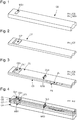
- the present description relates to a manufacturing method Pr1, the combined implementation of which makes it possible to manufacture a PC timepiece with a multi-level EH1 trim element such as that shown in FIG. figure 7 .
- the method Pr1 could apply to all kinds of parts, for example a piece of jewelry or jewelery, or a piece of tooling, and all kinds of elements of multi-level clothing. Finally, the piece could naturally have more than one dressing element.
- the Figures 1 to 3 show four layers CB, CT, CS and CL, which are then superimposed on each other during a superposition step of the manufacturing process.
- Each of the layers CB, CT, CS and CL is metallic, or metal alloy, or mineral.
- a layer is mineral, some of its zones must be made electrically conductive, for example by a physical vapor deposition technique (or PVD for the English "Physical Vapor Deposition"), as explained in the following of the description.
- step Pr1_fMB1 the basic pattern MB1 is formed by depositing a uniform layer (varnish or other) which is then selectively ablated by laser
- the figure 2 shows an intermediate layer CT comprising a first through hole OT1.
- the intermediate layer CT is formed of a metal alloy plate, for example brass, which is cut, for example by laser, to obtain the first hole OT1.
- the first hole OT1 is smaller than the first opening OS1 of the figure 3 .
- the figure 3 shows an additional layer CS comprising a first aperture OS1 through, an additional pattern MS3, and areas of reduced thickness ZS.
- the additional layer CS is superimposed on an electrically insulating layer CL comprising a first orifice OL1, an additional orifice OL3 and zones of excess thickness ZL.
- the areas of reduced thickness ZS of the additional layer CS could alternatively be zones of overthickness. In this case, the areas of extra thickness ZL would be areas of reduced thickness.
- the additional layer CS was obtained by a Pr1_fCS forming step of said layer according to the method Pr1.
- the additional layer CS is formed of a metal alloy plate, for example brass, which is cut, for example by laser, to obtain the first opening OS1.
- the plate is previously textured, for example guilloche or brushed.
- the additional layer CS is stamped so as to create a fingerprint forming an additional pattern MS3 such as that visible in FIG. figure 3 .
- step Pr1_fCS zones ZS of the additional layer CS are etched, so as to reduce their thickness, as represented in FIG. figure 3 .
- all these substeps of the step Pr1_fCS are not mandatory, only some of them can be realized.
- SC walls visible at the figure 5 of the basic pattern MB1, the first orifice OL1, the first opening OS1, the first hole OT1, and the exposed walls of the base layer CB are made conductive, for example by PVD deposition of a conductive film.
- the PVD deposition of the conductive film is only necessary on non-initially conducting faces.
- only some of the aforementioned walls undergo PVD deposition or any other equivalent treatment in order to make them conductive.
- an SCL portion of the upper face of the insulating layer CL that is to say the non-contacting surface with the upper layer CS
- the periphery of the first orifice OL1 can also be made conductive.
- the walls of the additional pattern MS3, the additional orifice OL3, and the exposed walls of the additional layer CS are the same for the walls of the additional pattern MS3, the additional orifice OL3, and the exposed walls of the additional layer CS. Similarly, a portion of the upper face of the diaper insulation CL at the periphery of the additional orifice OL3 can also be made conductive.
- the figure 5 schematically represents a pr1_gal galvanic deposition step of a metal layer or CM alloy on the inner faces of the first orifice OL1, the first opening OS1, the first hole OT1, on the faces of the base pattern MB and on the faces exposed base layer CB, according to the method Pr1.
- the four layers CB, CT, CS and CL superimposed are immersed in a galvanic bath suitable for the deposition of a metal such as gold, silver, nickel, or any other metal or metal alloy that can be deposited in relatively thick layer, to undergo electroforming.
- the electroforming is completed when the aforementioned walls are completely covered with the metal layer or alloy CM and that the thickness of the shell obtained is considered sufficient.
- the metal or alloy layer CM then comprises a lateral zone EL which rests on the insulating layer CL.
- the lateral zone EL extends at least in part on said portion SCL.
- a metal or alloy layer is similarly deposited on the walls of the additional orifice OL3, the additional pattern MS3 and on the exposed walls of the additional layer CS.
- the lateral zone EL extends at least in part over said portion.
- the metal or alloy CM layer forms a shell of a certain thickness. Then, in a step not shown, the insulating layer CL is dissolved by passing through suitable baths. The lateral zone EL is then optionally cut, depending on the type of part to be produced. Cutting the lateral zone EL is interesting if the part to be manufactured is a punch-type tool, for example.
- the figure 6 schematically represents a step of recovery or incrustation Pr1_rec of the additional layer CS and the metal layer or alloy CM, by a volume VL of a base material of the part to be manufactured, according to the method Pr1.
- the base material is amorphous or partially amorphous metal, interesting for its mechanical properties.
- the base material is a polymer or a composite (polymer ceramic, carbon fiber composite, etc.). In these two cases, a block of metal or metal alloy or of amorphous or partially amorphous alloy, or of polymer or composite, is pressed on the additional layer CS and against the metal or alloy layer CM at a temperature of which has a pasty consistency.
- the base material can be cast.
- the base material is any other metal or metal alloy, for example nickel, gold, etc., and the coating is made by galvanic growth of said metal.
- the volume VL is not entirely made up of the base material of the part.
- only part of the volume is made of the base material of the part, while the other part is made of a second material, advantageously less expensive than the base material.
- the part of volume VL consisting of the second the material advantageously fills the space inside the alloy metal shell, while the volume portions VL made of the base material are located in the visible, external locations of the part.
- the figure 7 schematically represents an extraction step Pr1_ext, volume VL and metal layers or CM alloys, according to the method Pr1.
- the volume VL and the metal or alloy layers CM are separated from the additional layer CS, the intermediate layer CT and the base layer CB.
- the assembly is for example immersed in a selective acid bath in which the additional layer CS, the intermediate layer CT and the base layer CB are dissolved.
- the separation is carried out by force demolding.
- a surface treatment of the additional layer CS facilitates demolding. This treatment is for example the application of a release agent or a passivation treatment.
- the volume VL then forms the body of the part PC, and the metal or alloy layers CM form the covering element EH1 (the additional covering element, resulting from the duplication of the supplementary pattern MS3, is not not represented on the figure 7 ). It is therefore understood that the shapes and dimensions of the cladding elements are directly dependent on the shapes and dimensions of the patterns, as well as the shapes and dimensions of the various orifices, openings and holes involved during the processes.
- the disengagement of the trim elements from the volume of base material is impossible without destroying the part.
- the interfaces between the workpiece body and the cladding elements are clear.
- the workpiece body is textured.
Landscapes
- Chemical & Material Sciences (AREA)
- Engineering & Computer Science (AREA)
- Manufacturing & Machinery (AREA)
- Chemical Kinetics & Catalysis (AREA)
- Organic Chemistry (AREA)
- Metallurgy (AREA)
- Materials Engineering (AREA)
- Physics & Mathematics (AREA)
- General Physics & Mathematics (AREA)
- Electrochemistry (AREA)
- Crystallography & Structural Chemistry (AREA)
- Microelectronics & Electronic Packaging (AREA)
- General Chemical & Material Sciences (AREA)
- Mechanical Engineering (AREA)
- Toxicology (AREA)
- Health & Medical Sciences (AREA)
- Micromachines (AREA)
- Adornments (AREA)
- Particle Formation And Scattering Control In Inkjet Printers (AREA)
- Laminated Bodies (AREA)
Description
L'invention se rapporte à un procédé de fabrication d'une pièce telle qu'une pièce d'horlogerie, de joaillerie ou de bijouterie, par exemple un cadran de montre, une lunette, une couronne, un maillon de bracelet, un fermoir, etc., ou encore une pièce d'outillage telle qu'un outil de frappe, un moule, etc. Le procédé permet plus particulièrement de réaliser une pièce comprenant un corps de pièce et un élément d'habillage multi-niveaux en relief sur le corps de la pièce, l'élément d'habillage étant tel qu'un indicateur des heures, un élément décoratif, une lettre, etc. Par multi-niveaux, on entend que l'élément comporte au moins deux faces planes visibles qui s'étendent parallèlement l'une à l'autre et parallèlement au corps de la pièce.The invention relates to a method of manufacturing a piece such as a timepiece, jewelery or jewelery, for example a watch face, a bezel, a crown, a bracelet link, a clasp, etc., or a piece of tooling such as a striking tool, a mold, etc. The method more particularly makes it possible to produce a part comprising a workpiece body and a multi-level dressing element embossed on the body of the workpiece, the cladding element being such that an hour indicator, a decorative element , a letter, etc. Multilevel means that the element comprises at least two visible planar faces which extend parallel to each other and parallel to the body of the part.
Dans le domaine de l'horlogerie, la joaillerie ou la bijouterie, il est classique de réaliser des éléments d'habillage multi-niveaux par des techniques de photolithographie et de dépôt galvanique. Le document
- se munir d'un substrat comportant une surface conductrice
- recouvrir la surface conductrice du substrat d'une première couche de résine photosensible
- irradier la première couche de résine photosensible à travers un masque correspondant à une empreinte désirée
- développer la première couche de résine photosensible de manière à creuser dans celle-ci des ouvertures et à obtenir ainsi un premier niveau d'un moule en résine, les ouvertures dans la première couche de résine laissant apparaître la surface conductrice du substrat
- déposer une nouvelle couche de résine photosensible sur la couche de résine développée, de manière à recouvrir cette dernière et, de préférence, à remplir les ouvertures dans celle-ci
- irradier la nouvelle couche de résine photosensible à travers un masque correspondant à l'empreinte désirée
- développer la nouvelle couche de résine photosensible de manière à creuser dans celle-ci des ouvertures et à obtenir un moule en résine multi-niveaux, les ouvertures dans le moule multi-niveaux laissant apparaître la surface conductrice du substrat
- remplir les ouvertures du moule en résine multi-niveaux d'un métal ou d'un alliage, par dépôt galvanique
- éliminer les couches de résine de manière à faire apparaître un élément métallique ou d'alliage multi-niveaux constitué par ledit métal ou alliage déposé dans les ouvertures.
- provide a substrate with a conductive surface
- covering the conductive surface of the substrate with a first layer of photoresist
- irradiating the first photoresist layer through a mask corresponding to a desired imprint
- developing the first layer of photosensitive resin so as to dig openings therein and thereby obtain a first level of a resin mold, the openings in the first resin layer revealing the conductive surface of the substrate
- depositing a new layer of photoresist on the layer of resin developed, so as to cover the latter and, preferably, to fill the openings therein
- irradiate the new layer of photoresist through a mask corresponding to the desired imprint
- developing the new layer of photosensitive resin so as to dig openings therein and to obtain a multi-level resin mold, the openings in the multi-level mold revealing the conductive surface of the substrate
- fill the openings of the multi-level resin mold of a metal or alloy, by galvanic deposition
- removing the resin layers so as to reveal a metal element or multi-level alloy consisting of said metal or alloy deposited in the openings.
Les éléments multi-niveaux ainsi fabriqués sont ensuite séparés du substrat et implantés sur un corps de pièce d'horlogerie, de joaillerie ou de bijouterie.The multi-level elements thus manufactured are then separated from the substrate and implanted on a timepiece, jewelery or jewelery body.
Ce procédé de fabrication de pièces dotées d'éléments d'habillage multi-niveaux présente l'inconvénient d'être long à mettre en oeuvre, notamment à cause de la nécessité de remplir intégralement les ouvertures du moule lors du dépôt galvanique. Un deuxième inconvénient est la nécessité d'un assemblage des éléments d'habillage sur le corps de pièce, d'où des risques de désolidarisation en cas de chocs, par exemple.This method of manufacturing parts with multi-level trim elements has the disadvantage of being long to implement, especially because of the need to completely fill the openings of the mold during the galvanic deposition. A second disadvantage is the need for an assembly of the cladding elements on the body of the room, hence the risk of disengagement in case of shocks, for example.
La présente invention vise à pallier en tout ou en partie les inconvénients évoqués précédemment.The present invention aims to overcome all or part of the disadvantages mentioned above.
A cet effet, l'invention se rapporte à un procédé de fabrication d'une pièce dotée d'un élément d'habillage, comportant les étapes suivantes :
- Superposer une couche électriquement isolante comportant un premier orifice traversant, une couche supplémentaire comportant une première ouverture traversante de dimensions similaires au premier orifice, une couche intermédiaire comprenant un premier trou traversant, et une couche de base surmontée d'un motif de base, de sorte à placer le motif de base dans le premier trou, recouvrir le premier trou par la première ouverture, et superposer la première ouverture et le premier orifice
- Déposer galvaniquement une couche métallique ou d'alliage métallique, de sorte qu'à l'issue de cette étape, la couche métallique ou d'alliage métallique forme une coque recouvrant des parois électriquement conductrices du motif de base, du premier orifice, de la première ouverture et du premier trou, et comporte une zone latérale reposant sur la couche isolante
- Dissoudre la couche isolante
- Recouvrir la couche métallique ou d'alliage métallique d'un volume constitué au moins en partie par un matériau de base de la pièce, de sorte que le volume épouse les formes de la couche métallique ou d'alliage métallique
- Extraire le volume et la couche métallique ou d'alliage métallique.
- Overlapping an electrically insulating layer having a first through hole, an additional layer having a first through opening of dimensions similar to the first port, an intermediate layer comprising a first through hole, and a base layer surmounted by a base pattern, so placing the base pattern in the first hole, covering the first hole with the first opening, and superimposing the first opening and the first hole
- Galvanically depositing a metal or metal alloy layer, so that at the end of this step, the metal or metal alloy layer forms a shell covering electrically conductive walls of the base pattern, the first orifice, the first opening and the first hole, and has a lateral zone resting on the insulating layer
- Dissolve the insulating layer
- Covering the metal or metal alloy layer with a volume formed at least in part by a base material of the workpiece, so that the volume conforms to the shapes of the metal layer or metal alloy
- Extract the volume and the metal layer or metal alloy.
Le procédé permet de fabriquer simultanément le corps de la pièce (constitué par le volume de matériau de base de la pièce) et l'élément d'habillage (constitué par la couche métallique ou d'alliage). L'élément d'habillage est directement fixé au corps de pièce, sans qu'il y ait besoin d'une étape d'assemblage. En effet, la zone latérale de la couche métallique ou d'alliage reposant sur la couche isolante à l'issue de la phase de dépôt, se retrouve scellée dans le volume à l'issue de la phase de recouvrement.The method makes it possible simultaneously to manufacture the body of the part (constituted by the volume of base material of the part) and the covering element (constituted by the metal or alloy layer). The cladding element is directly attached to the workpiece body, without the need for an assembly step. Indeed, the lateral zone of the metal layer or alloy resting on the insulating layer at the end of the deposition phase, is found sealed in the volume at the end of the recovery phase.
De plus, le procédé est plus rapide à mettre en oeuvre que le procédé de l'art antérieur précédemment décrit. En effet, la durée du dépôt galvanique est plus courte, car la couche métallique ou d'alliage n'a pas à remplir les orifices, ouvertures et trous (formant un moule), mais doit simplement recouvrir leurs parois ainsi que le motif. En d'autres termes, la structure métallique ou en alliage métallique n'est pas massive, elle forme au contraire une coque creuse. L'épaisseur à déposer par galvanoplastie est donc plus faible.In addition, the method is faster to implement than the method of the prior art described above. Indeed, the duration of the galvanic deposition is shorter, because the metal or alloy layer does not have to fill the holes, openings and holes (forming a mold), but simply needs to cover their walls as well as the pattern. In other words, the metal structure or metal alloy is not massive, it instead forms a hollow shell. The thickness to be deposited by electroplating is therefore lower.
Les interfaces entre le corps de pièce et l'élément d'habillage sont nettes, sans bavure. De plus, en choisissant des formes et dimensions appropriées pour les différents motifs, ouvertures, orifices ou trous intervenant dans les procédés de fabrication, il est possible de réaliser des éléments d'habillage de formes et de dimensions variées. En outre, une texture se trouvant sur la couche supplémentaire se retrouve gravée par effet d'empreinte sur le corps de pièce (le volume de matériau de base de la pièce).The interfaces between the workpiece body and the cladding element are sharp without burrs. Moreover, by choosing appropriate shapes and dimensions for the various patterns, openings, or holes or holes involved in the manufacturing processes, it is possible to produce trim elements of various shapes and sizes. In addition, a texture on the additional layer is imprinted on the workpiece (the volume of base material of the workpiece).
En outre, le procédé de fabrication peut comprendre une ou plusieurs des caractéristiques ci-dessous, prises indépendamment ou selon toutes les combinaisons techniquement possibles.In addition, the manufacturing method may include one or more of the features below, taken independently or in any technically possible combination.
Selon un mode de réalisation non limitatif, le procédé comporte une étape de formation de surfaces électriquement conductrices sur les parois du motif de base, du premier orifice, de la première ouverture et/ou du premier trou, par exemple par une technique de dépôt physique par phase vapeur.According to a non-limiting embodiment, the method comprises a step of forming electrically conductive surfaces on the walls of the base pattern, the first orifice, the first opening and / or the first hole, for example by a physical deposition technique. by vapor phase.
Selon un mode de réalisation non limitatif, le procédé comporte une étape de formation d'une surface électriquement conductrice sur une portion d'une face supérieure de la couche isolante située en périphérie du premier orifice.According to a non-limiting embodiment, the method comprises a step of forming an electrically conductive surface on a portion of an upper face of the insulating layer located at the periphery of the first orifice.
Selon un mode de réalisation non limitatif, le procédé comprend une étape de formation du motif de base sur la couche de base, comportant une application, une irradiation et un développement d'une résine photosensible, par exemple une résine SU8.According to a non-limiting embodiment, the method comprises a step of forming the base pattern on the base layer, comprising an application, an irradiation and a development of a photosensitive resin, for example an SU8 resin.
Selon un mode de réalisation non limitatif, le procédé comprend une étape de formation de la couche de base à partir d'un wafer en silicium, comportant un revêtement dudit wafer par un film conducteur.According to a non-limiting embodiment, the method comprises a step of forming the base layer from a silicon wafer, comprising a coating of said wafer with a conductive film.
Selon un mode de réalisation non limitatif, le procédé comporte une étape de formation de surfaces électriquement conductrices sur les parois du motif intermédiaire, du deuxième orifice et/ou de la deuxième ouverture.According to a non-limiting embodiment, the method comprises a step of forming electrically conductive surfaces on the walls of the intermediate pattern, the second orifice and / or the second opening.
Selon un mode de réalisation non limitatif, le procédé comporte une étape de formation d'une surface électriquement conductrice sur une portion d'une face supérieure de la couche isolante située en périphérie du deuxième orifice.According to a non-limiting embodiment, the method comprises a step of forming an electrically conductive surface on a portion of an upper face of the insulating layer located at the periphery of the second orifice.
Selon un mode de réalisation non limitatif, le procédé comporte une étape de formation du motif intermédiaire sur la couche intermédiaire, comportant une application, une irradiation et un développement d'une résine photosensible, par exemple une résine SU8.According to one nonlimiting embodiment, the method comprises a step of forming the intermediate pattern on the intermediate layer, comprising an application, an irradiation and a development of a photosensitive resin, for example an SU8 resin.
Selon un mode de réalisation non limitatif, le procédé comporte une étape de formation de la couche intermédiaire comportant une découpe, par exemple au laser, d'une plaque, par exemple en laiton.According to a non-limiting embodiment, the method comprises a step of forming the intermediate layer comprising cutting, for example by laser, a plate, for example brass.
Selon un mode de réalisation non limitatif, le procédé comporte une étape de formation de la couche supplémentaire comportant une découpe, par exemple au laser, d'une plaque, par exemple en laiton.According to a non-limiting embodiment, the method comprises a step of forming the additional layer comprising a cutting, for example by laser, of a plate, for example brass.
Selon un mode de réalisation non limitatif, l'étape de formation de la couche supplémentaire comprend un estampillage de la couche supplémentaire de sorte à y former un motif supplémentaire, la couche électriquement isolante comportant un orifice supplémentaire, l'orifice supplémentaire étant placé en regard du motif supplémentaire lorsque le couche isolante et la couche supplémentaire sont superposées.According to one nonlimiting embodiment, the step of forming the additional layer comprises a stamping of the additional layer so as to form an additional pattern, the electrically insulating layer having an additional orifice, the additional orifice being placed opposite additional pattern when the insulating layer and the additional layer are superimposed.
Selon un mode de réalisation non limitatif, l'étape de formation de la couche supplémentaire comprend une gravure de la couche supplémentaire de sorte à diminuer localement son épaisseur, la couche isolante comportant des zones de surépaisseur de sorte que l'ensemble comprenant la couche supplémentaire et la couche isolante superposées soit d'épaisseur constante.According to a non-limiting embodiment, the step of forming the additional layer comprises etching the additional layer so as to locally reduce its thickness, the insulating layer comprising areas of extra thickness so that the assembly comprising the additional layer and the superimposed insulating layer is of constant thickness.
Selon un mode de réalisation non limitatif, le procédé comporte une étape de formation de la couche isolante comportant une application, une irradiation et un développement d'une résine photosensible, par exemple une résine SU8, sur la couche supplémentaire, de sorte à former un orifice supplémentaire, l'orifice supplémentaire étant placé en regard du motif supplémentaire lorsque la couche isolante et la couche supplémentaire sont superposées.According to a nonlimiting embodiment, the method comprises a step of forming the insulating layer comprising an application, an irradiation and a development of a photosensitive resin, for example an SU8 resin, on the additional layer, so as to form a additional orifice, the additional orifice being placed opposite the additional pattern when the insulating layer and the additional layer are superimposed.
Selon un mode de réalisation non limitatif, le volume est constitué en partie d'un deuxième matériau, autre que le matériau de base, tel que le deuxième matériau remplit l'espace interne à la coque en métal ou en alliage métallique.According to a non-limiting embodiment, the volume is constituted in part by a second material, other than the base material, such that the second material fills the internal space to the shell of metal or metal alloy.
Selon un mode de réalisation non limitatif, le procédé comporte une étape de découpe de la zone latérale, réalisée avant l'étape de recouvrement.According to a non-limiting embodiment, the method comprises a step of cutting the lateral zone, made before the recovery step.
D'autres particularités et avantages ressortiront clairement de la description qui en est faite ci-après, à titre indicatif et nullement limitatif, en référence aux dessins annexés, dans lesquels :
- la
figure 1 est une représentation schématique d'une couche de base utilisée au sein d'un procédé selon un mode de réalisation non limitatif de l'invention, le procédé permettant de réaliser une pièce dotée d'au moins un élément d'habillage multi-niveaux - la
figure 2 est une représentation schématique d'une couche intermédiaire utilisée au sein du procédé - la
figure 3 est une représentation schématique d'une couche supplémentaire et d'une couche électriquement isolante, lesdites couches étant utilisées au sein du procédé - la
figure 4 représente une étape de superposition des couches desfigures 1, 2 et 3 , selon le procédé - la
figure 5 représente une étape de dépôt galvanique d'une couche métallique ou d'alliage selon le procédé - la
figure 6 représente une étape de recouvrement ou d'incrustation de la couche métallique ou d'alliage par un volume d'un matériau de base de la pièce selon le procédé - la
figure 7 représente la pièce finale obtenue par le procédé, la pièce étant dotée de deux éléments d'habillage multi-niveaux.
- the
figure 1 is a schematic representation of a base layer used in a method according to a non-limiting embodiment of the invention, the method for producing a part provided with at least one multi-level dressing element - the
figure 2 is a schematic representation of an intermediate layer used in the process - the
figure 3 is a schematic representation of an additional layer and an electrically insulating layer, said layers being used within the process - the
figure 4 represents a step of superposition of the layers ofFigures 1, 2 and 3 according to the method - the
figure 5 represents a step of galvanic deposition of a metal layer or alloy according to the method - the
figure 6 represents a step of recovery or incrustation of the metal layer or alloy by a volume of a base material of the part according to the method - the
figure 7 represents the final piece obtained by the method, the piece being provided with two elements of multi-level dressing.
La présente description porte sur un procédé de fabrication Pr1 dont la mise en oeuvre combinée permet de fabriquer une pièce PC d'horlogerie dotée d'un élément d'habillage EH1 multi-niveaux telle que celle représentée à la
Les
La
- application d'une résine photosensible sur la couche de base CB, par exemple une résine de type SU-8
- irradiation de la résine à travers un photomasque correspondant à la forme souhaitée du motif de base MB1, par rayons ultra-violets dans le cas d'une résine SU-8, pour polymériser une zone de la résine correspondant au motif de base MB1
- développement de la résine, pour dissoudre les zones non polymérisées et faire apparaître le motif de base MB1.
- applying a photoresist to the base layer CB, for example a SU-8 type resin
- irradiation of the resin through a photomask corresponding to the desired shape of the basic pattern MB1, by ultraviolet rays in the case of a SU-8 resin, to polymerize an area of the resin corresponding to the basic pattern MB1
- development of the resin, to dissolve the unpolymerized zones and to reveal the basic pattern MB1.
Dans un autre mode de réalisation non limitatif de l'étape Pr1_fMB1, le motif de base MB1 est formé par dépôt d'une couche uniforme (de vernis ou autre) qui est ensuite sélectivement ablatée par laserIn another non-limiting embodiment of step Pr1_fMB1, the basic pattern MB1 is formed by depositing a uniform layer (varnish or other) which is then selectively ablated by laser
La
La
La couche supplémentaire CS a été obtenue par une étape de formation Pr1_fCS de ladite couche selon le procédé Pr1. Dans un mode de réalisation non limitatif de l'étape Pr1_fCS, la couche supplémentaire CS est formée d'une plaque en alliage métallique, par exemple en laiton, que l'on découpe, par exemple au laser, pour obtenir la première ouverture OS1. On note que dans un mode de réalisation non limitatif de l'étape Pr1_fCS, la plaque est préalablement texturée, par exemple guillochée ou brossée. En outre, dans un mode de réalisation non limitatif de l'étape Pr1_fCS, la couche supplémentaire CS est estampillée de sorte à créer une empreinte formant un motif supplémentaire MS3 tel que celui visible à la
La couche isolante CL a été obtenue par une étape de formation Pr1_fCL de ladite couche selon le procédé. Dans un mode de réalisation non limitatif de l'étape Pr1_fCL, la couche isolante CL est obtenue par :
- application d'une résine photosensible sur la couche supplémentaire CS, par exemple une résine de type SU-8. On note que la résine présente alors des zones de surépaisseur ZL au niveau des zones d'épaisseur réduite de la couche supplémentaire CS, ou inversement si la couche supplémentaire CS comporte des zones de surépaisseur.
- irradiation de la résine à travers un photomasque, par rayons ultra-violets dans le cas d'une résine SU-8, pour polymériser la résine à l'exception des zones en regard de la première ouverture OS1 et du motif supplémentaire MS3
- développement de la résine, pour dissoudre les zones non polymérisées et faire apparaître un premier orifice OL1 superposé à la première ouverture OS1, et un orifice supplémentaire OL3 en regard du motif supplémentaire MS3.
- applying a photoresist to the additional layer CS, for example a SU-8 type resin. It is noted that the resin then has areas of extra thickness ZL at the reduced thickness areas of the additional layer CS, or conversely if the additional layer CS has areas of extra thickness.
- irradiation of the resin through a photomask, by ultraviolet rays in the case of a resin SU-8, to polymerize the resin except for the zones opposite the first opening OS1 and additional pattern MS3
- development of the resin, to dissolve the uncured areas and reveal a first orifice OL1 superimposed on the first opening OS1, and an additional orifice OL3 next to the additional pattern MS3.
La
- le motif de base MB1 est positionné dans le premier trou OT1, le premier trou OT1 est recouvert par la première ouverture OS1, et le premier orifice OL1 est superposé à la première ouverture OS1
- le motif supplémentaire MS3 est positionné en regard de l'orifice supplémentaire OL3.
- the basic pattern MB1 is positioned in the first hole OT1, the first hole OT1 is covered by the first opening OS1, and the first hole OL1 is superimposed on the first opening OS1
- the additional pattern MS3 is positioned opposite the additional orifice OL3.
Puis, dans une étape non représentée, des parois SC (visibles à la
Il en est de même pour des parois du motif supplémentaire MS3, de l'orifice supplémentaire OL3, et des parois exposées de la couche supplémentaire CS. De même, une portion de la face supérieure de la couche isolante CL en périphérie de l'orifice supplémentaire OL3 peut également être rendue conductrice.It is the same for the walls of the additional pattern MS3, the additional orifice OL3, and the exposed walls of the additional layer CS. Similarly, a portion of the upper face of the diaper insulation CL at the periphery of the additional orifice OL3 can also be made conductive.
La
De même, une couche métallique ou d'alliage est déposée de manière similaire sur les parois de l'orifice supplémentaire OL3, du motif supplémentaire MS3 et sur les parois exposées de la couche supplémentaire CS. Dans le cas où une portion de la face supérieure de la couche isolante CL en périphérie de l'orifice supplémentaire OL3 a été rendue conductrice, la zone latérale EL s'étend au moins en partie sur ladite portion.Similarly, a metal or alloy layer is similarly deposited on the walls of the additional orifice OL3, the additional pattern MS3 and on the exposed walls of the additional layer CS. In the case where a portion of the upper face of the insulating layer CL at the periphery of the additional orifice OL3 has been made conductive, the lateral zone EL extends at least in part over said portion.
La couche métallique ou d'alliage CM forme une coque d'une certaine épaisseur. Puis, dans une étape non représentée, on dissout la couche isolante CL par passage dans des bains adaptés. La zone latérale EL est alors éventuellement découpée, en fonction du type de pièce à réaliser. Découper la zone latérale EL est intéressant si la pièce à fabriquer est un outillage de type poinçon par exemple.The metal or alloy CM layer forms a shell of a certain thickness. Then, in a step not shown, the insulating layer CL is dissolved by passing through suitable baths. The lateral zone EL is then optionally cut, depending on the type of part to be produced. Cutting the lateral zone EL is interesting if the part to be manufactured is a punch-type tool, for example.
La
Dans un mode de réalisation alternatif de l'étape de recouvrement/d'incrustation Pr1_rec, le volume VL n'est pas intégralement constitué du matériau de base de la pièce. Dans ce cas, une partie seulement du volume est constituée du matériau de base de la pièce, tandis que l'autre partie est constituée d'un deuxième matériau, avantageusement moins cher que le matériau de base. La partie du volume VL constituée du deuxième matériau remplit ainsi avantageusement l'espace interne à la coque en métal en alliage, tandis que les parties du volume VL constituées du matériau de base sont situées aux endroits visibles, externes, de la pièce.In an alternative embodiment of the overlay step Pr1_rec, the volume VL is not entirely made up of the base material of the part. In this case, only part of the volume is made of the base material of the part, while the other part is made of a second material, advantageously less expensive than the base material. The part of volume VL consisting of the second Thus, the material advantageously fills the space inside the alloy metal shell, while the volume portions VL made of the base material are located in the visible, external locations of the part.
La
Le volume VL forme alors le corps de la pièce PC, et les couches métalliques ou d'alliages CM forment l'élément d'habillage EH1 (l'élément d'habillage supplémentaire, résultant de la duplication du motif supplémentaire MS3, n'est pas représenté sur la
Grâce aux procédés décrits, le désengagement des éléments d'habillage du volume de matériau de base est impossible sans détruire la pièce. De plus, on note que les interfaces entre le corps de pièce et les éléments d'habillage sont nettes. Par ailleurs, par un effet d'empreinte de la texture de la couche supplémentaire sur le volume se produisant lors de l'étape de recouvrement, le corps de pièce est texturé.With the methods described, the disengagement of the trim elements from the volume of base material is impossible without destroying the part. In addition, it is noted that the interfaces between the workpiece body and the cladding elements are clear. On the other hand, by imprinting the texture of the additional layer on the volume occurring during the covering step, the workpiece body is textured.
Bien entendu, la présente invention ne se limite pas à l'exemple illustré mais est susceptible de diverses variantes et modifications qui apparaîtront à l'homme de l'art, en particulier en ce qui concerne le nombre des couches superposées, les formes et dimensions des différents orifices, ouvertures, trous, motifs, etc.Of course, the present invention is not limited to the illustrated example but is susceptible of various variations and modifications which will occur to those skilled in the art, in particular as regards the number of superposed layers, the shapes and dimensions different holes, openings, holes, patterns, etc.
Claims (11)
- Method (Pr1) for fabrication of a piece (PC) provided with an exterior element (EH1), comprising the following ordered steps:- Superposing (Pr1_sup) an electrically insulating layer (CL) including a first through orifice (OL1), an additional layer (CS) including a first through aperture (OS1) of similar dimensions to the first orifice (OL1), an intermediate layer (CT) including a first through hole (OT1), and a base layer (CB) surmounted by a base motif (MB1), so as to place the base motif (MB1) inside the first hole (OT1), cover the first hole (OT1) with the first aperture (OS1), and superpose the first aperture (OS1) and the first orifice (OL1)- Electrodepositing (Pr1_gal) a metal or metal alloy layer (CM), so that at the end of this step, the metal or metal alloy layer (CM) forms a shell covering electrically conductive walls of the base motif (MB1), of the first orifice (OL1), of the first aperture (OS1) and of the first hole (OT1), and comprises a lateral area (EL) resting on the insulating layer (CL)- Dissolving the insulating layer (CL)- Coating (Pr1_rec) the metal or metal alloy layer (CM) with a volume (VL) at least partly formed by a base material of the piece (PC), so that the volume (VL) conforms to the shapes of the metal or metal alloy layer (CM)- Removing (Pr1_ext) the volume (VL) and the metal or metal alloy layer (CM).
- Method (Pr1) according to the preceding claim, including a step of forming electrically conductive surfaces (SC) on the walls of the base motif (MB1), of the first orifice (OL1), of the first aperture (OS1) and/or of the first hole (OT1), for example by a physical vapour deposition technique.
- Method (Pr1) according to the preceding claim, including a step of forming an electrically conductive surface (SCL) on one portion of an upper face of the insulating layer (CL) located at the periphery of the first orifice (OL1).
- Method (Pr1) according to any of the preceding claims, including a step (Pr1_fMB1) of forming the base motif (MB1) on the base layer (CB), including an application, irradiation and development of a photosensitive resin, for example an SU-8 resin.
- Method (Pr1) according to any of the preceding claims, including a step (Pr1_fCB) of forming the base layer (CB) from a silicon wafer, including coating said wafer with a conductive film.
- Method (Pr1) according to any of the preceding claims, including a step (Pr1_fCT) of forming the intermediate layer (CT) including cutting, for example laser cutting, of a plate, for example made of brass.
- Method (Pr1) according to any of the preceding claims, including a step (Pr1_fCS) of forming the additional layer (CS) including cutting, for example laser cutting, of a plate, for example made of brass.
- Method (Pr1) according to the preceding claim, the step (Pr1_fCS) of forming the additional layer (CS) including stamping the additional layer (CS) so as to form therein an additional motif (MS3), the electrically insulating layer (CL) including a third orifice (OL3), the third orifice (OL3) being placed facing the additional motif (MS3) when the insulating layer (CL) and the additional layer (CS) are superposed.
- Method (Pr1) according to any of claims 7 or 8, the step (Pr1_fCS) of forming the additional layer (CS) including an etch of the additional layer (CS) to locally diminish the thickness thereof, the insulating layer (CL) including areas of excess thickness so that the assembly comprising the superposed additional layer (CS) and insulating layer (CL) is of constant thickness.
- Method (Pr1) according to any of claims 8 or 9, including a step (Pr1_fCL) of forming the insulating layer (CL) including an application, irradiation and development of a photosensitive resin, for example an SU-8 resin, on the additional layer (CS), so as to form a third orifice (OL3), the third orifice (OL3) being placed facing the additional motif (MS3) when the insulating layer (CL) and the additional layer (CS) are superposed.
- Method (Pr1) according to any of the preceding claims, characterized the volume (VL) is partly formed of a second material, different from the base material, so that the second material fills the space inside the metal or metal alloy shell.
Priority Applications (5)
| Application Number | Priority Date | Filing Date | Title |
|---|---|---|---|
| EP16178118.2A EP3266738B1 (en) | 2016-07-06 | 2016-07-06 | Method for manufacturing a part for a timepiece provided with a multi-level exterior element |
| JP2017130236A JP6526748B2 (en) | 2016-07-06 | 2017-07-03 | Method of manufacturing a timepiece comprising a multilevel outer element |
| US15/640,650 US10301732B2 (en) | 2016-07-06 | 2017-07-03 | Method for fabrication of a timepiece provided with a multi-level exterior element |
| CN201710542563.7A CN107587171B (en) | 2016-07-06 | 2017-07-05 | For manufacturing the method for being equipped with the clock and watch of multi-layer outer member |
| HK18108417.8A HK1248777A1 (en) | 2016-07-06 | 2018-06-29 | Method for fabrication of a timepiece provided with a multi-level exterior element |
Applications Claiming Priority (1)
| Application Number | Priority Date | Filing Date | Title |
|---|---|---|---|
| EP16178118.2A EP3266738B1 (en) | 2016-07-06 | 2016-07-06 | Method for manufacturing a part for a timepiece provided with a multi-level exterior element |
Publications (2)
| Publication Number | Publication Date |
|---|---|
| EP3266738A1 EP3266738A1 (en) | 2018-01-10 |
| EP3266738B1 true EP3266738B1 (en) | 2019-03-06 |
Family
ID=56360304
Family Applications (1)
| Application Number | Title | Priority Date | Filing Date |
|---|---|---|---|
| EP16178118.2A Active EP3266738B1 (en) | 2016-07-06 | 2016-07-06 | Method for manufacturing a part for a timepiece provided with a multi-level exterior element |
Country Status (5)
| Country | Link |
|---|---|
| US (1) | US10301732B2 (en) |
| EP (1) | EP3266738B1 (en) |
| JP (1) | JP6526748B2 (en) |
| CN (1) | CN107587171B (en) |
| HK (1) | HK1248777A1 (en) |
Families Citing this family (1)
| Publication number | Priority date | Publication date | Assignee | Title |
|---|---|---|---|---|
| EP4206829A1 (en) * | 2021-12-28 | 2023-07-05 | Montres Breguet S.A. | Trim component for timepiece or jewellery item and method for manufacturing such a trim component |
Family Cites Families (13)
| Publication number | Priority date | Publication date | Assignee | Title |
|---|---|---|---|---|
| US2594820A (en) * | 1947-04-10 | 1952-04-29 | Stern Charles | Process for manufacturing timepiece dials |
| US5242711A (en) * | 1991-08-16 | 1993-09-07 | Rockwell International Corp. | Nucleation control of diamond films by microlithographic patterning |
| US6189448B1 (en) * | 1997-11-07 | 2001-02-20 | O'neal Dennis | Dual image stencil apparatus having stencil including sections with curled edges |
| JPH11323592A (en) * | 1998-05-14 | 1999-11-26 | Athene Kk | Electroformed metallic body and its production |
| JP2009516080A (en) * | 2005-11-18 | 2009-04-16 | レプリソールス テクノロジーズ アーベー | Electrode and method for forming the same |
| EP1916567B1 (en) * | 2006-10-26 | 2010-04-07 | Mimotec S.A. | Mixed manufacturing method for parts by photolithography, adding inserts and electroforming |
| EP2060534A1 (en) * | 2007-11-16 | 2009-05-20 | Nivarox-FAR S.A. | Composite silicon-metal micromechanical component and method for manufacturing same |
| CH704572B1 (en) | 2007-12-31 | 2012-09-14 | Nivarox Sa | A method of manufacturing a metal microstructure and microstructure obtained using this method. |
| EP2157476A1 (en) | 2008-08-20 | 2010-02-24 | Nivarox-FAR S.A. | Method of manufacturing multi-level metal parts using the LIGA-UV technique |
| EP2405300A1 (en) * | 2010-07-09 | 2012-01-11 | Mimotec S.A. | Manufacturing method for multi-level metal parts through an LIGA type method and parts obtained using the method |
| CH708827A2 (en) * | 2013-11-08 | 2015-05-15 | Nivarox Sa | micromechanical part hollow, several functional levels and a one-piece based on a synthetic allotrope of carbon material. |
| EP3009896B1 (en) * | 2014-10-17 | 2020-03-11 | Nivarox-FAR S.A. | Integral part made of electroformed metal |
| CH710531A2 (en) * | 2014-12-17 | 2016-06-30 | Nivarox Far Sa | Process for producing a component decorated with a timepiece or jewelery, and component produced by the method. |
-
2016
- 2016-07-06 EP EP16178118.2A patent/EP3266738B1/en active Active
-
2017
- 2017-07-03 US US15/640,650 patent/US10301732B2/en active Active
- 2017-07-03 JP JP2017130236A patent/JP6526748B2/en active Active
- 2017-07-05 CN CN201710542563.7A patent/CN107587171B/en active Active
-
2018
- 2018-06-29 HK HK18108417.8A patent/HK1248777A1/en unknown
Non-Patent Citations (1)
| Title |
|---|
| None * |
Also Published As
| Publication number | Publication date |
|---|---|
| CN107587171A (en) | 2018-01-16 |
| US10301732B2 (en) | 2019-05-28 |
| JP6526748B2 (en) | 2019-06-05 |
| US20180016686A1 (en) | 2018-01-18 |
| EP3266738A1 (en) | 2018-01-10 |
| CN107587171B (en) | 2019-10-15 |
| JP2018003158A (en) | 2018-01-11 |
| HK1248777A1 (en) | 2018-10-19 |
Similar Documents
| Publication | Publication Date | Title |
|---|---|---|
| EP3035125B1 (en) | Method for manufacturing a multi-level clock component | |
| EP2230208B1 (en) | Electroplating mould and method for manufacturing the same | |
| EP3536826B1 (en) | Method for producing a metal decoration on a dial and dial obtained according to said method | |
| EP2405300A1 (en) | Manufacturing method for multi-level metal parts through an LIGA type method and parts obtained using the method | |
| CH713871B1 (en) | Clock component comprising graphic elements of various aspects and method of manufacturing such a component. | |
| EP3034461B1 (en) | Production of a multi-level clock component | |
| EP3839624B1 (en) | Method for manufacturing a timepiece component | |
| CH704086B1 (en) | Multilevel metal parts obtained by a process LIGA and manufacturing method relating thereto. | |
| EP3266738B1 (en) | Method for manufacturing a part for a timepiece provided with a multi-level exterior element | |
| EP3951512A1 (en) | Method for manufacturing a part comprising at least one three-dimensional metallised pattern | |
| EP3839626B1 (en) | Method for manufacturing a timepiece component | |
| EP3839625A1 (en) | Method for manufacturing a timepiece component and component produced by this method | |
| EP3802920B1 (en) | Method for producing a metal decoration on a dial and dial obtained according to said method | |
| EP3246767B1 (en) | Method for manufacturing a timepiece provided with a hollow or raised casing element | |
| EP2745177B1 (en) | Method for implanting a decoration in a timepiece element deposited by electroplating | |
| EP3786722A1 (en) | Method for decorating a mechanical part | |
| CH712650A2 (en) | A method of manufacturing a watch, jewelery or jewelery piece with a multi-level trim element. | |
| EP2672320B1 (en) | Method for producing three-dimensional metal micro-parts by growth in a mixed cavity and micro-parts obtained by the method | |
| EP3246766B1 (en) | Method for manufacturing a timepiece provided with a raised casing element | |
| EP3839627B1 (en) | Method for manufacturing a micromould for electroforming of micromechanical components | |
| EP3839659B1 (en) | Method for decorating a mechanical part | |
| CH716969A2 (en) | A method of manufacturing a watch component and a component obtained according to this method. | |
| EP3841433B1 (en) | Method for manufacturing a timepiece component and component produced by this method | |
| CH708454A2 (en) | A method of processing a photosensitive resin layer and process for producing a metallic component. | |
| CH716967A2 (en) | A method of manufacturing a watch component and a component obtained according to this method. |
Legal Events
| Date | Code | Title | Description |
|---|---|---|---|
| PUAI | Public reference made under article 153(3) epc to a published international application that has entered the european phase |
Free format text: ORIGINAL CODE: 0009012 |
|
| STAA | Information on the status of an ep patent application or granted ep patent |
Free format text: STATUS: THE APPLICATION HAS BEEN PUBLISHED |
|
| AK | Designated contracting states |
Kind code of ref document: A1 Designated state(s): AL AT BE BG CH CY CZ DE DK EE ES FI FR GB GR HR HU IE IS IT LI LT LU LV MC MK MT NL NO PL PT RO RS SE SI SK SM TR |
|
| AX | Request for extension of the european patent |
Extension state: BA ME |
|
| STAA | Information on the status of an ep patent application or granted ep patent |
Free format text: STATUS: REQUEST FOR EXAMINATION WAS MADE |
|
| 17P | Request for examination filed |
Effective date: 20180710 |
|
| RBV | Designated contracting states (corrected) |
Designated state(s): AL AT BE BG CH CY CZ DE DK EE ES FI FR GB GR HR HU IE IS IT LI LT LU LV MC MK MT NL NO PL PT RO RS SE SI SK SM TR |
|
| RIC1 | Information provided on ipc code assigned before grant |
Ipc: G04B 19/04 20060101ALI20180813BHEP Ipc: B81C 99/00 20100101AFI20180813BHEP Ipc: C25D 1/00 20060101ALI20180813BHEP |
|
| GRAP | Despatch of communication of intention to grant a patent |
Free format text: ORIGINAL CODE: EPIDOSNIGR1 |
|
| STAA | Information on the status of an ep patent application or granted ep patent |
Free format text: STATUS: GRANT OF PATENT IS INTENDED |
|
| INTG | Intention to grant announced |
Effective date: 20180928 |
|
| GRAS | Grant fee paid |
Free format text: ORIGINAL CODE: EPIDOSNIGR3 |
|
| GRAA | (expected) grant |
Free format text: ORIGINAL CODE: 0009210 |
|
| STAA | Information on the status of an ep patent application or granted ep patent |
Free format text: STATUS: THE PATENT HAS BEEN GRANTED |
|
| AK | Designated contracting states |
Kind code of ref document: B1 Designated state(s): AL AT BE BG CH CY CZ DE DK EE ES FI FR GB GR HR HU IE IS IT LI LT LU LV MC MK MT NL NO PL PT RO RS SE SI SK SM TR |
|
| REG | Reference to a national code |
Ref country code: GB Ref legal event code: FG4D Free format text: NOT ENGLISH |
|
| REG | Reference to a national code |
Ref country code: CH Ref legal event code: EP Ref country code: AT Ref legal event code: REF Ref document number: 1104272 Country of ref document: AT Kind code of ref document: T Effective date: 20190315 |
|
| REG | Reference to a national code |
Ref country code: DE Ref legal event code: R096 Ref document number: 602016010594 Country of ref document: DE |
|
| REG | Reference to a national code |
Ref country code: IE Ref legal event code: FG4D Free format text: LANGUAGE OF EP DOCUMENT: FRENCH |
|
| REG | Reference to a national code |
Ref country code: CH Ref legal event code: NV Representative=s name: ICB INGENIEURS CONSEILS EN BREVETS SA, CH |
|
| REG | Reference to a national code |
Ref country code: NL Ref legal event code: MP Effective date: 20190306 |
|
| REG | Reference to a national code |
Ref country code: LT Ref legal event code: MG4D |
|
| PG25 | Lapsed in a contracting state [announced via postgrant information from national office to epo] |
Ref country code: SE Free format text: LAPSE BECAUSE OF FAILURE TO SUBMIT A TRANSLATION OF THE DESCRIPTION OR TO PAY THE FEE WITHIN THE PRESCRIBED TIME-LIMIT Effective date: 20190306 Ref country code: FI Free format text: LAPSE BECAUSE OF FAILURE TO SUBMIT A TRANSLATION OF THE DESCRIPTION OR TO PAY THE FEE WITHIN THE PRESCRIBED TIME-LIMIT Effective date: 20190306 Ref country code: NO Free format text: LAPSE BECAUSE OF FAILURE TO SUBMIT A TRANSLATION OF THE DESCRIPTION OR TO PAY THE FEE WITHIN THE PRESCRIBED TIME-LIMIT Effective date: 20190606 Ref country code: LT Free format text: LAPSE BECAUSE OF FAILURE TO SUBMIT A TRANSLATION OF THE DESCRIPTION OR TO PAY THE FEE WITHIN THE PRESCRIBED TIME-LIMIT Effective date: 20190306 |
|
| PG25 | Lapsed in a contracting state [announced via postgrant information from national office to epo] |
Ref country code: GR Free format text: LAPSE BECAUSE OF FAILURE TO SUBMIT A TRANSLATION OF THE DESCRIPTION OR TO PAY THE FEE WITHIN THE PRESCRIBED TIME-LIMIT Effective date: 20190607 Ref country code: RS Free format text: LAPSE BECAUSE OF FAILURE TO SUBMIT A TRANSLATION OF THE DESCRIPTION OR TO PAY THE FEE WITHIN THE PRESCRIBED TIME-LIMIT Effective date: 20190306 Ref country code: NL Free format text: LAPSE BECAUSE OF FAILURE TO SUBMIT A TRANSLATION OF THE DESCRIPTION OR TO PAY THE FEE WITHIN THE PRESCRIBED TIME-LIMIT Effective date: 20190306 Ref country code: HR Free format text: LAPSE BECAUSE OF FAILURE TO SUBMIT A TRANSLATION OF THE DESCRIPTION OR TO PAY THE FEE WITHIN THE PRESCRIBED TIME-LIMIT Effective date: 20190306 Ref country code: LV Free format text: LAPSE BECAUSE OF FAILURE TO SUBMIT A TRANSLATION OF THE DESCRIPTION OR TO PAY THE FEE WITHIN THE PRESCRIBED TIME-LIMIT Effective date: 20190306 Ref country code: BG Free format text: LAPSE BECAUSE OF FAILURE TO SUBMIT A TRANSLATION OF THE DESCRIPTION OR TO PAY THE FEE WITHIN THE PRESCRIBED TIME-LIMIT Effective date: 20190606 |
|
| REG | Reference to a national code |
Ref country code: AT Ref legal event code: MK05 Ref document number: 1104272 Country of ref document: AT Kind code of ref document: T Effective date: 20190306 |
|
| PG25 | Lapsed in a contracting state [announced via postgrant information from national office to epo] |
Ref country code: AL Free format text: LAPSE BECAUSE OF FAILURE TO SUBMIT A TRANSLATION OF THE DESCRIPTION OR TO PAY THE FEE WITHIN THE PRESCRIBED TIME-LIMIT Effective date: 20190306 Ref country code: ES Free format text: LAPSE BECAUSE OF FAILURE TO SUBMIT A TRANSLATION OF THE DESCRIPTION OR TO PAY THE FEE WITHIN THE PRESCRIBED TIME-LIMIT Effective date: 20190306 Ref country code: RO Free format text: LAPSE BECAUSE OF FAILURE TO SUBMIT A TRANSLATION OF THE DESCRIPTION OR TO PAY THE FEE WITHIN THE PRESCRIBED TIME-LIMIT Effective date: 20190306 Ref country code: IT Free format text: LAPSE BECAUSE OF FAILURE TO SUBMIT A TRANSLATION OF THE DESCRIPTION OR TO PAY THE FEE WITHIN THE PRESCRIBED TIME-LIMIT Effective date: 20190306 Ref country code: CZ Free format text: LAPSE BECAUSE OF FAILURE TO SUBMIT A TRANSLATION OF THE DESCRIPTION OR TO PAY THE FEE WITHIN THE PRESCRIBED TIME-LIMIT Effective date: 20190306 Ref country code: EE Free format text: LAPSE BECAUSE OF FAILURE TO SUBMIT A TRANSLATION OF THE DESCRIPTION OR TO PAY THE FEE WITHIN THE PRESCRIBED TIME-LIMIT Effective date: 20190306 Ref country code: SK Free format text: LAPSE BECAUSE OF FAILURE TO SUBMIT A TRANSLATION OF THE DESCRIPTION OR TO PAY THE FEE WITHIN THE PRESCRIBED TIME-LIMIT Effective date: 20190306 Ref country code: PT Free format text: LAPSE BECAUSE OF FAILURE TO SUBMIT A TRANSLATION OF THE DESCRIPTION OR TO PAY THE FEE WITHIN THE PRESCRIBED TIME-LIMIT Effective date: 20190706 |
|
| PG25 | Lapsed in a contracting state [announced via postgrant information from national office to epo] |
Ref country code: PL Free format text: LAPSE BECAUSE OF FAILURE TO SUBMIT A TRANSLATION OF THE DESCRIPTION OR TO PAY THE FEE WITHIN THE PRESCRIBED TIME-LIMIT Effective date: 20190306 Ref country code: SM Free format text: LAPSE BECAUSE OF FAILURE TO SUBMIT A TRANSLATION OF THE DESCRIPTION OR TO PAY THE FEE WITHIN THE PRESCRIBED TIME-LIMIT Effective date: 20190306 |
|
| REG | Reference to a national code |
Ref country code: DE Ref legal event code: R097 Ref document number: 602016010594 Country of ref document: DE |
|
| PG25 | Lapsed in a contracting state [announced via postgrant information from national office to epo] |
Ref country code: IS Free format text: LAPSE BECAUSE OF FAILURE TO SUBMIT A TRANSLATION OF THE DESCRIPTION OR TO PAY THE FEE WITHIN THE PRESCRIBED TIME-LIMIT Effective date: 20190706 Ref country code: AT Free format text: LAPSE BECAUSE OF FAILURE TO SUBMIT A TRANSLATION OF THE DESCRIPTION OR TO PAY THE FEE WITHIN THE PRESCRIBED TIME-LIMIT Effective date: 20190306 |
|
| PLBE | No opposition filed within time limit |
Free format text: ORIGINAL CODE: 0009261 |
|
| STAA | Information on the status of an ep patent application or granted ep patent |
Free format text: STATUS: NO OPPOSITION FILED WITHIN TIME LIMIT |
|
| PG25 | Lapsed in a contracting state [announced via postgrant information from national office to epo] |
Ref country code: DK Free format text: LAPSE BECAUSE OF FAILURE TO SUBMIT A TRANSLATION OF THE DESCRIPTION OR TO PAY THE FEE WITHIN THE PRESCRIBED TIME-LIMIT Effective date: 20190306 |
|
| 26N | No opposition filed |
Effective date: 20191209 |
|
| PG25 | Lapsed in a contracting state [announced via postgrant information from national office to epo] |
Ref country code: SI Free format text: LAPSE BECAUSE OF FAILURE TO SUBMIT A TRANSLATION OF THE DESCRIPTION OR TO PAY THE FEE WITHIN THE PRESCRIBED TIME-LIMIT Effective date: 20190306 Ref country code: MC Free format text: LAPSE BECAUSE OF FAILURE TO SUBMIT A TRANSLATION OF THE DESCRIPTION OR TO PAY THE FEE WITHIN THE PRESCRIBED TIME-LIMIT Effective date: 20190306 |
|
| PG25 | Lapsed in a contracting state [announced via postgrant information from national office to epo] |
Ref country code: TR Free format text: LAPSE BECAUSE OF FAILURE TO SUBMIT A TRANSLATION OF THE DESCRIPTION OR TO PAY THE FEE WITHIN THE PRESCRIBED TIME-LIMIT Effective date: 20190306 |
|
| REG | Reference to a national code |
Ref country code: BE Ref legal event code: MM Effective date: 20190731 |
|
| PG25 | Lapsed in a contracting state [announced via postgrant information from national office to epo] |
Ref country code: LU Free format text: LAPSE BECAUSE OF NON-PAYMENT OF DUE FEES Effective date: 20190706 Ref country code: BE Free format text: LAPSE BECAUSE OF NON-PAYMENT OF DUE FEES Effective date: 20190731 |
|
| PG25 | Lapsed in a contracting state [announced via postgrant information from national office to epo] |
Ref country code: IE Free format text: LAPSE BECAUSE OF NON-PAYMENT OF DUE FEES Effective date: 20190706 |
|
| GBPC | Gb: european patent ceased through non-payment of renewal fee |
Effective date: 20200706 |
|
| PG25 | Lapsed in a contracting state [announced via postgrant information from national office to epo] |
Ref country code: GB Free format text: LAPSE BECAUSE OF NON-PAYMENT OF DUE FEES Effective date: 20200706 |
|
| PG25 | Lapsed in a contracting state [announced via postgrant information from national office to epo] |
Ref country code: CY Free format text: LAPSE BECAUSE OF FAILURE TO SUBMIT A TRANSLATION OF THE DESCRIPTION OR TO PAY THE FEE WITHIN THE PRESCRIBED TIME-LIMIT Effective date: 20190306 |
|
| PG25 | Lapsed in a contracting state [announced via postgrant information from national office to epo] |
Ref country code: MT Free format text: LAPSE BECAUSE OF FAILURE TO SUBMIT A TRANSLATION OF THE DESCRIPTION OR TO PAY THE FEE WITHIN THE PRESCRIBED TIME-LIMIT Effective date: 20190306 Ref country code: HU Free format text: LAPSE BECAUSE OF FAILURE TO SUBMIT A TRANSLATION OF THE DESCRIPTION OR TO PAY THE FEE WITHIN THE PRESCRIBED TIME-LIMIT; INVALID AB INITIO Effective date: 20160706 |
|
| PG25 | Lapsed in a contracting state [announced via postgrant information from national office to epo] |
Ref country code: MK Free format text: LAPSE BECAUSE OF FAILURE TO SUBMIT A TRANSLATION OF THE DESCRIPTION OR TO PAY THE FEE WITHIN THE PRESCRIBED TIME-LIMIT Effective date: 20190306 |
|
| P01 | Opt-out of the competence of the unified patent court (upc) registered |
Effective date: 20230615 |
|
| PGFP | Annual fee paid to national office [announced via postgrant information from national office to epo] |
Ref country code: CH Payment date: 20230801 Year of fee payment: 8 |
|
| PGFP | Annual fee paid to national office [announced via postgrant information from national office to epo] |
Ref country code: FR Payment date: 20240619 Year of fee payment: 9 |
|
| PGFP | Annual fee paid to national office [announced via postgrant information from national office to epo] |
Ref country code: DE Payment date: 20240619 Year of fee payment: 9 |