EP2249630A1 - Circuit board - Google Patents
Circuit board Download PDFInfo
- Publication number
- EP2249630A1 EP2249630A1 EP08710907A EP08710907A EP2249630A1 EP 2249630 A1 EP2249630 A1 EP 2249630A1 EP 08710907 A EP08710907 A EP 08710907A EP 08710907 A EP08710907 A EP 08710907A EP 2249630 A1 EP2249630 A1 EP 2249630A1
- Authority
- EP
- European Patent Office
- Prior art keywords
- circuit board
- pull
- face
- tabs
- release papers
- Prior art date
- Legal status (The legal status is an assumption and is not a legal conclusion. Google has not performed a legal analysis and makes no representation as to the accuracy of the status listed.)
- Withdrawn
Links
Images


Classifications
-
- H—ELECTRICITY
- H05—ELECTRIC TECHNIQUES NOT OTHERWISE PROVIDED FOR
- H05K—PRINTED CIRCUITS; CASINGS OR CONSTRUCTIONAL DETAILS OF ELECTRIC APPARATUS; MANUFACTURE OF ASSEMBLAGES OF ELECTRICAL COMPONENTS
- H05K3/00—Apparatus or processes for manufacturing printed circuits
- H05K3/0058—Laminating printed circuit boards onto other substrates, e.g. metallic substrates
-
- H—ELECTRICITY
- H05—ELECTRIC TECHNIQUES NOT OTHERWISE PROVIDED FOR
- H05K—PRINTED CIRCUITS; CASINGS OR CONSTRUCTIONAL DETAILS OF ELECTRIC APPARATUS; MANUFACTURE OF ASSEMBLAGES OF ELECTRICAL COMPONENTS
- H05K1/00—Printed circuits
- H05K1/02—Details
- H05K1/03—Use of materials for the substrate
- H05K1/0393—Flexible materials
-
- H—ELECTRICITY
- H05—ELECTRIC TECHNIQUES NOT OTHERWISE PROVIDED FOR
- H05K—PRINTED CIRCUITS; CASINGS OR CONSTRUCTIONAL DETAILS OF ELECTRIC APPARATUS; MANUFACTURE OF ASSEMBLAGES OF ELECTRICAL COMPONENTS
- H05K2201/00—Indexing scheme relating to printed circuits covered by H05K1/00
- H05K2201/09—Shape and layout
- H05K2201/09009—Substrate related
- H05K2201/09109—Locally detached layers, e.g. in multilayer
-
- H—ELECTRICITY
- H05—ELECTRIC TECHNIQUES NOT OTHERWISE PROVIDED FOR
- H05K—PRINTED CIRCUITS; CASINGS OR CONSTRUCTIONAL DETAILS OF ELECTRIC APPARATUS; MANUFACTURE OF ASSEMBLAGES OF ELECTRICAL COMPONENTS
- H05K2203/00—Indexing scheme relating to apparatus or processes for manufacturing printed circuits covered by H05K3/00
- H05K2203/02—Details related to mechanical or acoustic processing, e.g. drilling, punching, cutting, using ultrasound
- H05K2203/0264—Peeling insulating layer, e.g. foil, or separating mask
-
- H—ELECTRICITY
- H05—ELECTRIC TECHNIQUES NOT OTHERWISE PROVIDED FOR
- H05K—PRINTED CIRCUITS; CASINGS OR CONSTRUCTIONAL DETAILS OF ELECTRIC APPARATUS; MANUFACTURE OF ASSEMBLAGES OF ELECTRICAL COMPONENTS
- H05K2203/00—Indexing scheme relating to apparatus or processes for manufacturing printed circuits covered by H05K3/00
- H05K2203/02—Details related to mechanical or acoustic processing, e.g. drilling, punching, cutting, using ultrasound
- H05K2203/0271—Mechanical force other than pressure, e.g. shearing or pulling
-
- H—ELECTRICITY
- H05—ELECTRIC TECHNIQUES NOT OTHERWISE PROVIDED FOR
- H05K—PRINTED CIRCUITS; CASINGS OR CONSTRUCTIONAL DETAILS OF ELECTRIC APPARATUS; MANUFACTURE OF ASSEMBLAGES OF ELECTRICAL COMPONENTS
- H05K3/00—Apparatus or processes for manufacturing printed circuits
- H05K3/38—Improvement of the adhesion between the insulating substrate and the metal
- H05K3/386—Improvement of the adhesion between the insulating substrate and the metal by the use of an organic polymeric bonding layer, e.g. adhesive
Definitions
- the present invention relates to a circuit board having adhesive layers covered with release papers.
- each circuit board (each printed wiring board) on which the above-mentioned semiconductor packages and the like are mounted is formed with more than one layer, and flexible multilayer circuit boards are often used as the circuit boards.
- Such a multilayer circuit board having the above-mentioned semiconductor packages mounted thereon is placed and secured in, for example, a thin housing with a small mounting space.
- a so-called screw securing method or an adhering method is employed.
- the latter which is an adhering method, is for securing a wiring board in a housing by virtue of the viscoelasticity of an adhesive layer. Accordingly, the adhering method excels in shock resistance, compared with the former method, which is the screw securing method. Since the wiring board can be secured simply by pressing the appropriate portion of the wiring board against the inner wall or the like of the housing, the adhering method excels in workability in the mounting process.
- FIG. 7 illustrates an example of a flexible circuit board that secures a wiring board by a conventional adhering method. More specifically, in the example illustrated in FIG. 7 , an adhesive layer (not shown) and a release paper 2 covering the adhesive layer are bonded to one face of a circuit board 1 formed into an L-shape. The end portion of the release paper 2 is designed to stick out of the circuit board 1, and function as a pull-tab 2p to be used for removing the release paper 2.
- the multilayer circuit board 1 has appropriate electronic components mounted on a face other than the face to which the release paper 2 is bonded, or on the back side of the drawing.
- the release paper 2 is removed from the circuit board 1 by using the pull-tab 2p, and the adhesive layer remaining on the face of the circuit board 1 is pressed against the inner wall (not shown) of the housing or the like. In this manner, the circuit board 1 can be mounted in a predetermined position in the housing.
- FIG. 8 a circuit board in which a release paper is bonded within a face of a circuit board, and two diagonal corners of the release paper are formed as pull-tabs, as shown in FIG. 8 .
- the release paper 2 having a rectangular adhesive layer is bonded to one face (the upper face in the drawing) of a circuit board 1 or an electronic component.
- Two diagonal corners of the release paper 2 are designed to be nonadhesive portions 2p having no adhesive layers, and the nonadhesive portions 2p are used as pull-tabs.
- Patent Document 1 Japanese Patent Application Laid-Open No. 2005-157012
- FIGS. 7 and 8 are designed as a structure in which a release paper is bonded to one face of a circuit board or the like. Therefore, in some products, it is preferable to bond two or more separate release papers to different locations on the circuit board face. In cases of such a structure, the following measures can be taken depending on the product: one of the release papers may be selectively removed while the other one is left, or the order of removing release paper may be determined based on the order of mounting the components and the like constituting the mechanism, for example.
- An object of the invention is to provide a circuit board that has plural separate release papers bonded to different locations on a circuit board face as described above, and has pull-tabs, placed at preferred locations, for selectively removing the respective release papers.
- a circuit board having adhesive layers has a release paper bonded to at least one face of the circuit board via an adhesive layer, the release paper covering the adhesive layer, wherein a plurality of separated release papers is bonded to the one face of the circuit board, a nonadhesive portion without an adhesive layer is formed on a portion of the one face of the circuit board located between each two adjacent release papers, and pull-tabs for removing the respective release papers are formed at end portions of the respective release papers located at the nonadhesive portion.
- the separated release papers are bonded, without sticking out of the one face of the circuit board.
- the pull-tabs for removing the respective release papers are designed to face each other at the nonadhesive portion.
- top end portions of the pull-tabs are designed to overlap with each other on the one face of the circuit board.
- the circuit board is preferably formed of a flexible multilayer board.
- two or more release papers are separated and bonded at different locations on a circuit board face. Accordingly, in some products, one of the release papers may be selectively removed while the other one is left, and part of the circuit board may be bonded. Also, the order of removing release paper may be determined based on the order of mounting the components and the like constituting the mechanism, for example. In this manner, a structure can be flexibly mounted on a housing or the like including a circuit board.
- the respective release papers are bonded to a face of a circuit board, without sticking out of the face, and a nonadhesive portion having no adhesive layers is formed on a portion of the circuit board face located between the adjacent release papers.
- the pull-tabs for removing the respective release papers can be formed at the adjacent end portions of the respective release papers, so as to face each other.
- the top end portions of the pull-tabs are designed to overlap with each other on the circuit board face, so that the order of removing the respective release papers is inevitably determined. Accordingly, the correct working sequence can be set. Furthermore, the indicators indicating the order of removal are provided on the pull-tabs or the release papers, so that the correct working sequence can be set.
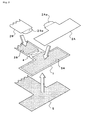
- FIG. 1 is a top view of the fundamental structure of the circuit board.
- FIG. 2 is a perspective view of a preferred exemplary stack structure of the circuit board.
- Reference numeral 1 denotes the circuit board.
- This circuit board 1 is formed into a T-shape as shown in the drawings, and is preferably a flexible multilayer board.
- Release papers are bonded to one face of the circuit board 1 via adhesive layers, and cover the adhesive layers.
- a release paper A (denoted by reference numeral 2A) and a release paper B (denoted by reference numeral 2B) are bonded to one face of the circuit board 1, so as not to stick out of the face of the circuit board 1.
- the release papers A and B are bonded to the circuit board 1 via adhesive layers 3A and 3B illustrated with hatchings of broken lines in FIGS. 1 and 2 .
- a nonadhesive portion 4 having no adhesive layers is formed at a location adjacent to the release papers A and B.
- the end portions of the release papers 2A and 2B located in the nonadhesive portion 4 are formed into circular arcs, and form pull-tabs 2Ap and 2Bp for removing the release papers 2A and 2B.
- the pull-tabs 2Ap and 2Bp for removing the release papers 2A and 2B or A and B are formed to face each other at the nonadhesive portion 4, and the top end portions of the pull-tabs are designed to overlap with each other on the face of the circuit board 1. More specifically, in this embodiment, the pull-tab 2Bp of the release paper 2B is the lower one of the two pull-tabs, and the pull-tab 2Ap of the release paper 2A is the upper one as shown in FIG. 1 .
- the release paper 2A illustrated as A is removed first. Accordingly, as described in the paragraph of the "Effects of the Invention", the order of removing the release papers can be inevitably determined, and the correct sequence of operation can be set.
- a reinforcing plate 5 having the same shape as the circuit board 1 is formed and stacked so as to line the circuit board 1, as shown in FIG. 2 .
- a composite board is formed.
- the reinforcing plate 5 is used when needed, and is not an essential component.
- the reinforcing plate 5 may be formed and stacked between the circuit board 1 and the adhesive layers 3A and 3B.
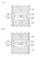
- FIG. 3 is a diagram for explaining another preferred example of the pull-tabs 2Ap and 2Bp that are formed in the nonadhesive portion 4 to remove the release papers 2A and 2B.
- the top end portions of the pull-tabs are designed to overlap with each other, as in the example illustrated in FIG. 1 .
- the pull-tab 2Bp of the release paper 2B is the lower one of the pull-tabs, and the pull-tab 2Ap of the release paper 2A is stacked on the pull-tab 2Bp.
- the pull-tabs 2Ap and 2Bp have indicators that indicate the order of removing the respective release papers 2A and 2B.
- a notch 2Am is formed in the upper pull-tab 2Ap, and two notches 2Bm are formed in the lower pull-tab 2Bp.
- FIG. 4 is a diagram for explaining yet another preferred example of the pull-tabs 2Ap and 2Bp for removing the respective release papers 2A and 2B formed in the nonadhesive portion 4.
- through holes are formed in the pull-tabs 2Ap and 2Bp, instead of the above-described notches. More specifically, one through hole 2Am is formed in the upper pull-tab 2Ap, and two through holes 2Bm are formed in the lower pull-tab 2Bp.
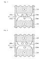
- FIGS. 5 and 6 are diagrams for explaining other preferred examples of the pull-tabs 2Ap and 2Bp for removing the release papers 2A and 2B formed in the nonadhesive portion 4.
- the respective pull-tabs 2Ap and 2Bp are designed not to overlap with each other in the nonadhesive portion 4, and the end portions of the respective pull-tabs face each other.
- indicators are provided in the form of notches or through holes formed in the pull-tabs.
- numerals or the like indicating the order of removal may be preferably printed on the pull-tabs or the release papers.
- the two release papers 2A and 2B are bonded to a circuit board face, while being separated from each other.
- the number of separated release papers may be three or more, for example.
Landscapes
- Engineering & Computer Science (AREA)
- Manufacturing & Machinery (AREA)
- Microelectronics & Electronic Packaging (AREA)
- Structure Of Printed Boards (AREA)
- Credit Cards Or The Like (AREA)
- Laminated Bodies (AREA)
- Production Of Multi-Layered Print Wiring Board (AREA)
Abstract
Description
- The present invention relates to a circuit board having adhesive layers covered with release papers.
- In response to the recent demands for high-performance, light-weight thin electronic devices, high-density integration and high-density mounting of electronic components are being developed. In this trend, the semiconductor packages used for the electronic devices are becoming smaller than ever, and are having more pins. Accordingly, each circuit board (each printed wiring board) on which the above-mentioned semiconductor packages and the like are mounted is formed with more than one layer, and flexible multilayer circuit boards are often used as the circuit boards. Such a multilayer circuit board having the above-mentioned semiconductor packages mounted thereon is placed and secured in, for example, a thin housing with a small mounting space.
- To place and secure the multilayer wiring board in the housing, a so-called screw securing method or an adhering method is employed. The latter, which is an adhering method, is for securing a wiring board in a housing by virtue of the viscoelasticity of an adhesive layer. Accordingly, the adhering method excels in shock resistance, compared with the former method, which is the screw securing method. Since the wiring board can be secured simply by pressing the appropriate portion of the wiring board against the inner wall or the like of the housing, the adhering method excels in workability in the mounting process.
-
FIG. 7 illustrates an example of a flexible circuit board that secures a wiring board by a conventional adhering method. More specifically, in the example illustrated inFIG. 7 , an adhesive layer (not shown) and arelease paper 2 covering the adhesive layer are bonded to one face of acircuit board 1 formed into an L-shape. The end portion of therelease paper 2 is designed to stick out of thecircuit board 1, and function as a pull-tab 2p to be used for removing therelease paper 2. Although not shown in the drawing, themultilayer circuit board 1 has appropriate electronic components mounted on a face other than the face to which therelease paper 2 is bonded, or on the back side of the drawing. - Accordingly, in the
circuit board 1 having the above-described structure, therelease paper 2 is removed from thecircuit board 1 by using the pull-tab 2p, and the adhesive layer remaining on the face of thecircuit board 1 is pressed against the inner wall (not shown) of the housing or the like. In this manner, thecircuit board 1 can be mounted in a predetermined position in the housing. - When a circuit board of this type is manufactured, a so-called multicavity technique is utilized to employ a large-size work board and divide the work board into two or more circuit boards in the end. In the circuit board having the structure illustrated in
FIG. 7 , however, the pull-tab 2p constituting part of therelease paper 2 sticks out of the face of thecircuit board 1, and the protruding portion is also regarded as part of the apparent circuit board. As a result, the number of circuit boards that can be obtained from a work board becomes smaller, which leads to cost increase. - To counter this problem, there is suggested a circuit board in which a release paper is bonded within a face of a circuit board, and two diagonal corners of the release paper are formed as pull-tabs, as shown in
FIG. 8 . More specifically, in the example illustrated inFIG. 8 , therelease paper 2 having a rectangular adhesive layer is bonded to one face (the upper face in the drawing) of acircuit board 1 or an electronic component. Two diagonal corners of therelease paper 2 are designed to benonadhesive portions 2p having no adhesive layers, and thenonadhesive portions 2p are used as pull-tabs. - With the structure illustrated in
FIG. 8 , thenonadhesive portions 2p functioning as pull-tabs are formed within a face of a circuit board or an electronic component. Accordingly, the problem with the structure illustrated inFIG. 7 can be solved. The structure of the circuit board illustrated inFIG. 8 is disclosed inPatent Document 1.
[Patent Document 1] Japanese Patent Application Laid-Open No.2005-157012 - Each of the structures illustrated in
FIGS. 7 and 8 is designed as a structure in which a release paper is bonded to one face of a circuit board or the like. Therefore, in some products, it is preferable to bond two or more separate release papers to different locations on the circuit board face. In cases of such a structure, the following measures can be taken depending on the product: one of the release papers may be selectively removed while the other one is left, or the order of removing release paper may be determined based on the order of mounting the components and the like constituting the mechanism, for example. - An object of the invention is to provide a circuit board that has plural separate release papers bonded to different locations on a circuit board face as described above, and has pull-tabs, placed at preferred locations, for selectively removing the respective release papers.
- To solve the above problems, a circuit board having adhesive layers according to the present invention has a release paper bonded to at least one face of the circuit board via an adhesive layer, the release paper covering the adhesive layer, wherein a plurality of separated release papers is bonded to the one face of the circuit board, a nonadhesive portion without an adhesive layer is formed on a portion of the one face of the circuit board located between each two adjacent release papers, and pull-tabs for removing the respective release papers are formed at end portions of the respective release papers located at the nonadhesive portion.
- In this case, the separated release papers are bonded, without sticking out of the one face of the circuit board. In addition, in a preferred embodiment, the pull-tabs for removing the respective release papers are designed to face each other at the nonadhesive portion. Furthermore, in one preferred example, top end portions of the pull-tabs are designed to overlap with each other on the one face of the circuit board.
- In addition, indicators that indicate the order of removal may be provided on the release papers or on the pull-tabs for removing the release papers. The circuit board is preferably formed of a flexible multilayer board.
- With the above-described structure of a circuit board, two or more release papers are separated and bonded at different locations on a circuit board face. Accordingly, in some products, one of the release papers may be selectively removed while the other one is left, and part of the circuit board may be bonded. Also, the order of removing release paper may be determined based on the order of mounting the components and the like constituting the mechanism, for example. In this manner, a structure can be flexibly mounted on a housing or the like including a circuit board.
- The respective release papers are bonded to a face of a circuit board, without sticking out of the face, and a nonadhesive portion having no adhesive layers is formed on a portion of the circuit board face located between the adjacent release papers. With this arrangement, the pull-tabs for removing the respective release papers can be formed at the adjacent end portions of the respective release papers, so as to face each other.
- In this case, the top end portions of the pull-tabs are designed to overlap with each other on the circuit board face, so that the order of removing the respective release papers is inevitably determined. Accordingly, the correct working sequence can be set. Furthermore, the indicators indicating the order of removal are provided on the pull-tabs or the release papers, so that the correct working sequence can be set.
-
-
FIG. 1 is a top view showing an embodiment of a circuit board according to the present invention. -
FIG. 2 is a perspective view showing an exemplary stack structure of the circuit board ofFIG. 1 . -
FIG. 3 is a partially enlarged view showing another preferred example of the pull-tabs for removing the respective release papers. -
FIG. 4 is a partially enlarged view showing still another preferred example of the pull-tabs. -
FIG. 5 is a partially enlarged view showing yet another preferred example of the pull-tabs. -
FIG. 6 is a partially enlarged view showing still yet another preferred example of the pull-tabs. -
FIG. 7 is a top view showing an example of a conventional circuit board. -
FIG. 8 is a perspective view showing another example of a conventional circuit board. -
- 1
- circuit board
- 2A, 2B
- release paper
- 2Ap, 2Bp
- pull-tab
- 2Am, 2Bm
- indicator
- 3A, 3B
- adhesive layer
- 4
- nonadhesive portion
- 5
- reinforcing plate
- A circuit board according to the present invention will be described below with reference to an embodiment illustrated in the accompanying drawings.
FIG. 1 is a top view of the fundamental structure of the circuit board.FIG. 2 is a perspective view of a preferred exemplary stack structure of the circuit board. -
Reference numeral 1 denotes the circuit board. Thiscircuit board 1 is formed into a T-shape as shown in the drawings, and is preferably a flexible multilayer board. Release papers are bonded to one face of thecircuit board 1 via adhesive layers, and cover the adhesive layers. In the embodiment illustrated in the drawings, a release paper A (denoted by reference numeral 2A) and a release paper B (denoted by reference numeral 2B) are bonded to one face of thecircuit board 1, so as not to stick out of the face of thecircuit board 1. - The release papers A and B are bonded to the
circuit board 1 via adhesive layers 3A and 3B illustrated with hatchings of broken lines inFIGS. 1 and2 . Anonadhesive portion 4 having no adhesive layers is formed at a location adjacent to the release papers A and B. The end portions of the release papers 2A and 2B located in thenonadhesive portion 4 are formed into circular arcs, and form pull-tabs 2Ap and 2Bp for removing the release papers 2A and 2B. - Therefore, in the embodiment illustrated in
FIGS. 1 and2 , the pull-tabs 2Ap and 2Bp for removing the release papers 2A and 2B or A and B are formed to face each other at thenonadhesive portion 4, and the top end portions of the pull-tabs are designed to overlap with each other on the face of thecircuit board 1. More specifically, in this embodiment, the pull-tab 2Bp of the release paper 2B is the lower one of the two pull-tabs, and the pull-tab 2Ap of the release paper 2A is the upper one as shown inFIG. 1 . - With the above structure, the release paper 2A illustrated as A is removed first. Accordingly, as described in the paragraph of the "Effects of the Invention", the order of removing the release papers can be inevitably determined, and the correct sequence of operation can be set.
- In the embodiment illustrated in the drawings, a reinforcing
plate 5 having the same shape as thecircuit board 1 is formed and stacked so as to line thecircuit board 1, as shown inFIG. 2 . In this manner, a composite board is formed. However, the reinforcingplate 5 is used when needed, and is not an essential component. Alternatively, the reinforcingplate 5 may be formed and stacked between thecircuit board 1 and the adhesive layers 3A and 3B. -
FIG. 3 is a diagram for explaining another preferred example of the pull-tabs 2Ap and 2Bp that are formed in thenonadhesive portion 4 to remove the release papers 2A and 2B. In the example illustrated inFIG. 3 , the top end portions of the pull-tabs are designed to overlap with each other, as in the example illustrated inFIG. 1 . The pull-tab 2Bp of the release paper 2B is the lower one of the pull-tabs, and the pull-tab 2Ap of the release paper 2A is stacked on the pull-tab 2Bp. - The pull-tabs 2Ap and 2Bp have indicators that indicate the order of removing the respective release papers 2A and 2B. In the example illustrated in
FIG. 3 , a notch 2Am is formed in the upper pull-tab 2Ap, and two notches 2Bm are formed in the lower pull-tab 2Bp. With this arrangement, it is possible to recognize that the release paper 2A having the one notch 2Am should be removed first, and the release paper 2B having the two notches 2Bm should be removed later. - In the structure illustrated in
FIG. 3 , even if the pull-tabs are overlapped the other way around during the operation to mount the board, the order of removing the respective release papers can be recognized from the number of notches formed in each of the pull-tabs 2Ap and 2Bp. -
FIG. 4 is a diagram for explaining yet another preferred example of the pull-tabs 2Ap and 2Bp for removing the respective release papers 2A and 2B formed in thenonadhesive portion 4. In the example illustrated inFIG. 4 , through holes are formed in the pull-tabs 2Ap and 2Bp, instead of the above-described notches. More specifically, one through hole 2Am is formed in the upper pull-tab 2Ap, and two through holes 2Bm are formed in the lower pull-tab 2Bp. - With this arrangement, it is possible to recognize that the release paper 2A having the one through hole 2Am formed therein is removed first, and the release paper 2B having the two through holes 2Bm formed therein is removed later. Accordingly, with the structure illustrated in
FIG. 4 , the same function effects as those in the example illustrated inFIG. 3 can be achieved. -
FIGS. 5 and 6 are diagrams for explaining other preferred examples of the pull-tabs 2Ap and 2Bp for removing the release papers 2A and 2B formed in thenonadhesive portion 4. In each of the examples illustrated inFIGS. 5 and 6 , the respective pull-tabs 2Ap and 2Bp are designed not to overlap with each other in thenonadhesive portion 4, and the end portions of the respective pull-tabs face each other. - In the example illustrated in
FIG. 5 , different numbers of notches 2Am and 2Bm are formed on the pull-tabs facing each other. In the example illustrated inFIG. 6 , different numbers of through holes 2Am and 2Bm are formed in the pull-tabs facing each other. Accordingly, it is possible to recognize the order of removing the respective release papers, according to the numbers of notches or through holes. - In the examples illustrated in
FIGS. 3 to 6 , indicators are provided in the form of notches or through holes formed in the pull-tabs. However, numerals or the like indicating the order of removal may be preferably printed on the pull-tabs or the release papers. - In the above-described embodiment, the two release papers 2A and 2B are bonded to a circuit board face, while being separated from each other. However, the number of separated release papers may be three or more, for example.
Claims (6)
- A circuit board that has a release paper bonded to at least one face of the circuit board via an adhesive layer, the release paper covering the adhesive layer,
wherein a plurality of separated release papers is bonded to the one face of the circuit board, a nonadhesive portion without an adhesive layer is formed on a portion of the one face of the circuit board located between each two adjacent release papers, and pull-tabs for removing the respective release papers are formed at end portions of the respective release papers located at the nonadhesive portion. - The circuit board according to claim 1, wherein the separated release papers are bonded, without sticking out of the one face of the circuit board.
- The circuit board according to claim 1 or 2, wherein the pull-tabs for removing the respective release papers are designed to face each other at the nonadhesive portion.
- The circuit board according to claim 3, wherein top end portions of the pull-tabs are designed to overlap with each other on the one face of the circuit board.
- The circuit board according to claim 1, wherein indicators that indicate the order of removal are provided on the release papers or on the pull-tabs for removing the release papers.
- The circuit board according to claim 1, which is formed of a flexible multilayer board.
Applications Claiming Priority (1)
| Application Number | Priority Date | Filing Date | Title |
|---|---|---|---|
| PCT/JP2008/052017 WO2009098765A1 (en) | 2008-02-07 | 2008-02-07 | Circuit board |
Publications (2)
| Publication Number | Publication Date |
|---|---|
| EP2249630A1 true EP2249630A1 (en) | 2010-11-10 |
| EP2249630A4 EP2249630A4 (en) | 2012-07-25 |
Family
ID=40951853
Family Applications (1)
| Application Number | Title | Priority Date | Filing Date |
|---|---|---|---|
| EP08710907A Withdrawn EP2249630A4 (en) | 2008-02-07 | 2008-02-07 | Circuit board |
Country Status (5)
| Country | Link |
|---|---|
| US (1) | US20100282497A1 (en) |
| EP (1) | EP2249630A4 (en) |
| KR (1) | KR20100110828A (en) |
| CN (1) | CN101940070A (en) |
| WO (1) | WO2009098765A1 (en) |
Families Citing this family (1)
| Publication number | Priority date | Publication date | Assignee | Title |
|---|---|---|---|---|
| US9723714B2 (en) * | 2015-10-20 | 2017-08-01 | Flexterra, Inc. | Electronic circuit device having a protective backing for low-velocity impacts and high-velocity impacts |
Family Cites Families (12)
| Publication number | Priority date | Publication date | Assignee | Title |
|---|---|---|---|---|
| JPS58148485A (en) * | 1982-02-27 | 1983-09-03 | 日本メクトロン株式会社 | Flexible circuit board with release sheet |
| SE455268B (en) * | 1986-05-23 | 1988-07-04 | Moelnlycke Ab | Needle PARTY TAPE |
| JPH0388367U (en) * | 1989-12-27 | 1991-09-10 | ||
| JPH04307987A (en) * | 1991-04-05 | 1992-10-30 | Canon Inc | Flexible wiring board for fixed tube attachment |
| CA2123003A1 (en) * | 1991-11-06 | 1993-05-13 | Dennis M. Kay | Occlusive wound dressing and applicator |
| JPH0550763U (en) * | 1991-12-03 | 1993-07-02 | 日本電産株式会社 | Flexible circuit board |
| JPH07307534A (en) * | 1994-05-12 | 1995-11-21 | Ibiden Co Ltd | Printed wiring board |
| JP3016144U (en) * | 1995-03-23 | 1995-09-26 | リバテープ製薬株式会社 | Waterproof wound protector |
| US6391138B1 (en) * | 1999-09-20 | 2002-05-21 | Molex Incorporated | Method of fabricating a laminated circuit assembly and product thereof |
| JP2004311907A (en) * | 2003-04-10 | 2004-11-04 | Olympus Corp | Packaging substrate |
| JP2005157012A (en) | 2003-11-27 | 2005-06-16 | Sharp Corp | Film mounting method, mounting apparatus, and electronic component manufacturing method using the same |
| JP4260800B2 (en) * | 2005-12-02 | 2009-04-30 | リバテープ製薬株式会社 | Adhesive plaster and method for producing the same |
-
2008
- 2008-02-07 WO PCT/JP2008/052017 patent/WO2009098765A1/en not_active Ceased
- 2008-02-07 CN CN2008801263628A patent/CN101940070A/en active Pending
- 2008-02-07 EP EP08710907A patent/EP2249630A4/en not_active Withdrawn
- 2008-02-07 KR KR1020107015863A patent/KR20100110828A/en not_active Withdrawn
- 2008-02-07 US US12/812,600 patent/US20100282497A1/en not_active Abandoned
Also Published As
| Publication number | Publication date |
|---|---|
| US20100282497A1 (en) | 2010-11-11 |
| CN101940070A (en) | 2011-01-05 |
| KR20100110828A (en) | 2010-10-13 |
| WO2009098765A1 (en) | 2009-08-13 |
| EP2249630A4 (en) | 2012-07-25 |
Similar Documents
| Publication | Publication Date | Title |
|---|---|---|
| US8519270B2 (en) | Circuit board and manufacturing method thereof | |
| KR101253401B1 (en) | Method of manufacturing for bonding pad | |
| KR20150125424A (en) | Rigid flexible printed circuit board and method of manufacturing the same | |
| US8426739B2 (en) | Printed circuit board and method for manufacturing the same, and panel for manufacturing the printed circuit board | |
| US20100282497A1 (en) | Circuit board | |
| US8563141B2 (en) | Carrier for manufacturing printed circuit board, method of manufacturing the same and method of manufacturing printed circuit board using the same | |
| JP5302927B2 (en) | Manufacturing method of multilayer wiring board | |
| JP4361325B2 (en) | Mounting substrate manufacturing method, electronic component mounting method, mounted substrate inspection method, mounted substrate dividing method, reinforcing substrate, and multilayer substrate | |
| JP2581729Y2 (en) | Flexible circuit board with reinforcing plate | |
| JPH10173299A (en) | Printed wiring board | |
| JP2008153483A (en) | Circuit board | |
| JP2015097227A (en) | Composite board | |
| JP4716199B2 (en) | Tamper-resistant structure | |
| WO2007135997A1 (en) | Printed board | |
| JP4072415B2 (en) | Flexible circuit board | |
| JPH0997956A (en) | Printed-circuit board | |
| JP2534005Y2 (en) | Multi-faced printed circuit board | |
| JPH1022590A (en) | Printed wiring board to take many faces | |
| JP2008159658A (en) | Circuit board | |
| JP3157875B2 (en) | Multi-layer flexible printed wiring board | |
| JPH11214807A (en) | Printed circuit board | |
| JPH07101462A (en) | Electronic parts | |
| KR200151370Y1 (en) | Machine Hole Reinforcement Structure of Array Printed Circuit Board | |
| JP4645261B2 (en) | Flexible printed circuit board | |
| JP3890717B2 (en) | Printed circuit board |
Legal Events
| Date | Code | Title | Description |
|---|---|---|---|
| PUAI | Public reference made under article 153(3) epc to a published international application that has entered the european phase |
Free format text: ORIGINAL CODE: 0009012 |
|
| 17P | Request for examination filed |
Effective date: 20100712 |
|
| AK | Designated contracting states |
Kind code of ref document: A1 Designated state(s): AT BE BG CH CY CZ DE DK EE ES FI FR GB GR HR HU IE IS IT LI LT LU LV MC MT NL NO PL PT RO SE SI SK TR |
|
| AX | Request for extension of the european patent |
Extension state: AL BA MK RS |
|
| DAX | Request for extension of the european patent (deleted) | ||
| A4 | Supplementary search report drawn up and despatched |
Effective date: 20120625 |
|
| RIC1 | Information provided on ipc code assigned before grant |
Ipc: H05K 3/00 20060101ALI20120619BHEP Ipc: B32B 15/08 20060101ALI20120619BHEP Ipc: H05K 1/02 20060101AFI20120619BHEP |
|
| STAA | Information on the status of an ep patent application or granted ep patent |
Free format text: STATUS: THE APPLICATION IS DEEMED TO BE WITHDRAWN |
|
| 18D | Application deemed to be withdrawn |
Effective date: 20120901 |