EP2244383A1 - Verfahren und Vorrichtung zur Steuerung einer Dämpferschaltung - Google Patents
Verfahren und Vorrichtung zur Steuerung einer Dämpferschaltung Download PDFInfo
- Publication number
- EP2244383A1 EP2244383A1 EP09158624A EP09158624A EP2244383A1 EP 2244383 A1 EP2244383 A1 EP 2244383A1 EP 09158624 A EP09158624 A EP 09158624A EP 09158624 A EP09158624 A EP 09158624A EP 2244383 A1 EP2244383 A1 EP 2244383A1
- Authority
- EP
- European Patent Office
- Prior art keywords
- snubber circuit
- switches
- input voltage
- voltage
- controlling
- Prior art date
- Legal status (The legal status is an assumption and is not a legal conclusion. Google has not performed a legal analysis and makes no representation as to the accuracy of the status listed.)
- Withdrawn
Links
Images

Classifications
-
- H—ELECTRICITY
- H03—ELECTRONIC CIRCUITRY
- H03K—PULSE TECHNIQUE
- H03K17/00—Electronic switching or gating, i.e. not by contact-making and –breaking
- H03K17/08—Modifications for protecting switching circuit against overcurrent or overvoltage
- H03K17/082—Modifications for protecting switching circuit against overcurrent or overvoltage by feedback from the output to the control circuit
-
- H—ELECTRICITY
- H02—GENERATION; CONVERSION OR DISTRIBUTION OF ELECTRIC POWER
- H02M—APPARATUS FOR CONVERSION BETWEEN AC AND AC, BETWEEN AC AND DC, OR BETWEEN DC AND DC, AND FOR USE WITH MAINS OR SIMILAR POWER SUPPLY SYSTEMS; CONVERSION OF DC OR AC INPUT POWER INTO SURGE OUTPUT POWER; CONTROL OR REGULATION THEREOF
- H02M1/00—Details of apparatus for conversion
- H02M1/32—Means for protecting converters other than automatic disconnection
- H02M1/34—Snubber circuits
Definitions
- the present invention relates generally to a method and an apparatus for controlling the operation of a snubber circuit.
- Snubber circuits are frequently used in electrical systems with an inductive load where the sudden interruption of current flow often leads to a sharp rise in voltage across the device creating the interruption. This sharp rise in voltage is a transient and can damage and lead to the failure of the semiconductor device. A spark is likely to be generated (arcing) and to cause electromagnetic interference.
- the snubber circuit prevents this undesired voltage by conducting transient current around the device.
- a simple snubber comprising a small resistor R S in series with a small capacitor C S is often used.
- the snubber circuit protects power devices against voltage breakdowns and also avoids electromagnetic interferences in order to comply with some rules and standards.
- Snubber circuits are often used in DC/DC converters.
- Classical DC/DC converters use inductors in order to convert a direct current from a first voltage to a second voltage which may be larger or smaller than the first voltage.
- Inductors are used for storing energy in the form of magnetic field (current) and they have many drawbacks. Inductors are heavy, their cost is relatively important because they are mainly composed of copper material.
- charge pumps also known as DC/DC converters use capacitors as energy storage elements.
- charge pumps offer unique characteristics that make them attractive for certain end-user applications.
- each bridge device is composed of four switches and a capacitor.
- the voltage on each bridge may be positive, null or negative according to the control of the switches. Dead-time needs to be applied between switching of the high side and low side switches of each bridge leg in order to avoid that the bridge capacitors may be short circuited.
- the dead-time may lead to some drawbacks, such as high voltage overshoots that appear on the switches. These overshoots will also appear in the input of the boost converter composed of plural bridge devices several times within a single switching period which is usually up to 2 k times, where k is the number of bridge devices.
- the input voltage variations are even more undesirable as there may represent loss of power generation due to the oscillations around the maximum power point (MPP) of the photovoltaic module.
- MPP maximum power point
- Snubber circuits avoid voltage overshoots and protect the switches.
- snubber circuit avoid voltage overshoots and the consequent power generation losses around the MPP.
- Periodical switching patterns are selected in order to provide different boost ratios. When the input voltage varies, it is sometimes necessary to select another switching pattern which provides another boost ratio.
- the input voltage of the photovoltaic module may vary during a certain time voltage levels which exist on each bridge capacitor for each duty-cycle case at equilibrium condition may be different between different boost ratios.
- the snubber circuit of the boost converter composed of plural bridge devices has to cope with such input voltage variation and large current peaks can be generated if the voltage imposed by the boost converter composed of plural bridge devices in the input is smaller than the voltage level on the snubber capacitor.
- the components of snubber circuits need then to be sized in order to cope with the large current peaks.
- the overall cost of the boost converter composed of plural bridge devices is then increased.
- the present invention aims at providing a method and an apparatus which provide the advantages of snubber circuits in normal operation conditions for a given duty-cycle, without the need of a snubber circuit which is able to withstand high currents.
- the present invention concerns an apparatus for controlling the operation of a snubber circuit in a system in which an input voltage is processed using at least switches controlled with at least one periodical pattern, characterised in that the input voltage is applied to the snubber circuit when the operation of the snubber circuit is enabled, and in that the apparatus comprises:
- the present invention concerns also a method for controlling the operation of a snubber circuit in a system in which an input voltage is processed using at least switches using at least one periodical pattern, characterised in that the input voltage is applied to the snubber circuit when the operation of the snubber circuit is enabled, and in that the method comprises the steps of:
- the switches used for processing the input voltage are switches of a boost converter composed of plural bridge devices.
- the means for enabling/disabling the operation of the snubber circuit are composed of a switch.
- the snubber circuit can be continuously connected to the boost converter composed of plural bridge devices, except for the moments in which high current could be generated due to its presence such as during the converter start-up and also during the duty-cycles changes.
- the means for enabling/disabling the operation of the snubber circuit are composed of two N-MOSFET transistors and their respective body diodes, connected in series and in opposite position.
- the anode of a first diode is connected to the source of a first N-MOSFET transistor S WS1 , the cathode of the first diode is connected to the drain of the first N-MOSFET transistor, the anode of a second diode is connected to the source of a second N-MOSFET transistor and the cathode of the second diode is connected to the drain of the second N-MOSFET transistor S WS and the drain of the first N-MOSFET transistor S WS1 is connected to the drain of the second N-MOSFET transistor.
- the snubber circuit is composed of a capacitor connected in series with a sub-circuit composed of a resistor and a diode connected in parallel.
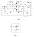
- Fig. 1 is an example of a boost converter composed of three bridge devices in which the present invention is implemented.
- the boost converter is also named Reactor Less Boost Converter or an inductor less boost converter, herein named RLBC.
- the present invention is described in a RLBC connected to a photovoltaic module.
- the present application is also applicable in any system wherein input voltage may vary and wherein switches and capacitors are used.
- the inductor of the conventional DC/DC Boost converter is replaced by "k" bridge devices connected in series.
- Each bridge device is composed of four switches and a capacitor as shown in Fig. 1 . It has to be noted here that two switches may be under the form of diodes acting as switches.
- This individual bridge structure is also named "bit”.
- the boost converter composed of plural bridge devices also contains an output stage comprising a diode Do and a capacitor Co.
- Fig. 1 three bits or bridge devices B1, B2 and B3 are shown and are connected in series; the third bit B3 is connected to the output stage.
- a boost converter comprising a more important number of bridge devices can be obtained by duplicating the bit B1 as much as necessary.
- the bit B1 is composed of four switches S 11 , S 12 , S 13 and S 14 and one capacitor C 1 .
- the switches S 11 and S 14 are the switches of the high side of the bit B1 and the switches S 12 and S 13 are the switches of the low side of the bit B1.
- the switches S 11 and S 12 are the switches of one leg of the bit B1 and the switches S 14 and S 13 are the switches of the other leg of the bit B1.
- the bit B2 is composed of four switches S 21 , S 22 , S 23 and S 24 and one capacitor C 2 .
- the switches S 21 and S 24 are the switches of the high side of the bit B2 and the switches S 22 and S 23 are the switches of the low side of the bit B2.
- the switches S 21 and S 22 are the switches of one leg of the bit B2 and the switches S 24 and S 23 are the switches of the other leg of the bit B2.
- the bit B3 is composed of three switches S 31 , S 32 and S 33 and one capacitor C 3 .
- the first terminal of the switch S i1 is connected to the second terminal of the switch S i2 .
- the second terminal of the switch S i1 is connected to the second terminal of the switch S i4 and to the positive terminal of the capacitor C i .
- the first terminal of the switch S i2 is connected to the negative terminal of the capacitor C i and to the first terminal of the switch S i3 .
- the first terminal of the switch S i4 is connected to the second terminal of the switch S i3 .
- Electric DC providing means like photovoltaic modules provide an input voltage Vin.
- the positive terminal of electric DC providing means is connected to the first terminal of the switch S 11 .
- the first terminal of the switch S 31 is connected to the second terminal of the switch S 32 .
- the second terminal of the switch S 31 is connected to anode of the diode Do and to the positive terminal of the capacitor C 3 .
- the first terminal of the switch S 32 is connected to the negative terminal of the capacitor C 3 and to the second terminal of the switch S 33 .
- the first terminal of the switch S 33 is connected to the negative terminal of electric DC providing means.
- the cathode of the diode Do is connected to the positive terminal of the capacitor C o .
- the negative terminal of the capacitor C O is connected to the negative terminal of electric DC providing means.
- the first terminal of the switch S 14 is connected to the first terminal of the switch S 21 .
- the first terminal of the switch S 24 is connected to the first terminal of the switch S 31 .
- the voltage on the capacitor C O is equal to Vout.
- Vb1 The difference of voltage between the input and the output of B1 is named Vb1
- Vb2 the difference of voltage between the input and the output of B2
- Vb3 the difference of voltage between the input and the output of B3 is named Vb3.
- Vb3 equals Vb3* when switch S 33 is on, and equals Vb3** when switch S 33 is off.
- V C1 The difference of voltage in C 1 is named V C1
- V C2 the difference of voltage in C 2
- V C3 the difference of voltage in C 3
- the RLBC further comprises a snubber circuit.
- the snubber circuit is composed of a diode D S , a resistor R S and a capacitor C S .
- the positive terminal of electric DC providing means is connected to the anode of the diode D S and to the first terminal of the resistor R S .
- the cathode of the diode D S is connected to the second terminal of the resistor R S and to a first terminal of the capacitor C S .
- a switch is provided in the present invention for enabling or disabling the operation of the snubber circuit.
- the second terminal of the capacitor C S is connected to the first terminal of the switch S WS .
- the second terminal of the switch S WS is connected to the negative terminal of electric DC providing means.
- Vc ⁇ 1 : Vc ⁇ 2 : ⁇ : Vcn 1 : 2 : ... 2 k - 1 ⁇ V CO / 2 k
- V CO is the stepped-up output voltage
- the switching pattern of the switches of each bridge Bi is defined so as to offer a voltage Vbi at the connectors of the bridge that equals + Vci, -Vci, or 0, where Vci is the voltage of the capacitor C i .
- the switching patterns are applied on the switches S 11 , S 12 , S 13 , S 14 , S 21 , S 22 , S 23 , S 245 S 315 S 32 and S 33 .
- the operation of a snubber circuit in a system in which an input voltage is processed using at least switches controlled with at least one periodical pattern is controlled.
- the input voltage is applied to the snubber circuit when the operation of snubber circuit is enabled.
- a periodical pattern to be used for controlling the switches is determined, the periodical pattern boosting the input voltage and which will cause some modification on the input voltage value during the transient state.
- the operation of the snubber circuit is disabled, the switches are controlled with the determined periodical pattern and it is checked if the transient state is over and the input voltage is stable.
- the operation of the snubber circuit is enabled if the input voltage is compatible with a given value.
- Fig. 2 represents an example of a switch for disconnecting or not the snubber circuit.
- the switch S WS is for example composed of two N-MOSFET transistors and their respective body diodes.
- the anode of the body diode D S1 is connected to the source of the N-MOSFET transistor S WS1 and the cathode of the body diode D S1 is connected to the drain of the N-MOSFET transistor S WS1 .
- the anode of the body diode D S2 is connected to the source of the N-MOSFET transistor S WS2 and the cathode of the body diode D S2 is connected to the drain of the N-MOSFET transistor S WS2 .
- the drain of the N-MOSFET transistor S WS1 is connected to the drain of the N-MOSFET transistor S WS2 .
- the source of the N-MOSFET transistor S WS2 is connected to the negative terminal of the electric DC providing means.
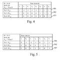
- Fig. 3 represents an example of a device comprising a boost converter composed of plural bridge devices.
- the device 30 has, for example, an architecture based on components connected together by a bus 301 and a processor 300 controlled by the program related to the algorithm as disclosed in the Fig. 6 .
- the device 30 is, in a variant, implemented under the form of one or several dedicated integrated circuits which execute the same operations as the one executed by the processor 300 as disclosed hereinafter.
- the bus 301 links the processor 300 to a read only memory ROM 302, a random access memory RAM 303, an analogue to digital converter ADC 306 and the RLBC module as the one disclosed in Fig. 1 .
- the read only memory ROM 302 contains instructions of the program related to the algorithm as disclosed in the Fig. 6 which are transferred, when the device 30 is powered on to the random access memory RAM 303.
- the read only memory ROM 302 memorizes the tables shown in Figs. 4 and 5 .
- the RAM memory 303 contains registers intended to receive variables, and the instructions of the program related to the algorithm as disclosed in the Fig. 6 .
- the analogue to digital converter 306 is connected to the RLBC and converts voltages representative of the input voltage Vin and/or the output voltage Vout into binary information.
- Fig. 4 is an example of voltage values on the bridges of the boost converter composed of three bridges in order to have a first step-up ratio when the periodical pattern is decomposed into eight time intervals.
- Vb1 V ref
- Vb1 -V ref
- Vb1 V ref
- Vb1 V ref
- Fig. 5 is an example of voltage values on the bridges of the boost converter composed of three bridges in order to have a second step-up ratio when the periodical pattern is decomposed into seven time intervals;
- Vb1 V ref
- Vb1 V ref
- Fig. 6 is an example of an algorithm for controlling the snubber circuit according to the present invention.
- the present algorithm is executed by the processor 300 of the device 30.
- the processor 200 gets the input voltage Vin that the boost converter composed of plural bridge devices has to boost.
- Vin could be the result of a measurement made by digital converter 306 of the input voltage applied to the boost converter composed of plural bridge devices.
- Vin could be determined by computation by processor 300 from yet other measurement made by digital converter 306 of other signals, such as bit voltages, output voltage, input or output currents, so as to realise a specific regulation function.
- the regulation function is determined so as to maximise the electrical power passing through the boost converter composed of plural bridge devices.
- the processor 300 checks the input voltage Vin boosted by the RLBC using a given duty cycle D, for example, the one provided by the periodical pattern corresponding to the table of the Fig. 4 .
- step S600 If the input voltage Vin provides an output voltage value which is comprised in a desired range of output voltage, the processor 300 returns to step S600. Otherwise, the processor 300 moves to step S602.
- the processor 300 sets the value of the variable Vprev to the value of Vin.
- the processor 300 disables the operation of the snubber circuit of the RLBC by transferring a command to the RLBC setting the switch S WS in non conductive state (OFF state).
- the processor 300 selects another duty cycle D which enables the boost of the input voltage to an output voltage value which is comprised in the desired range of output voltage. For example, the processor 300 selects the duty cycle D provided by the periodical pattern corresponding to the table of the Fig. 5 .
- the processor 300 commands the switches of the RLBC 305 according to the pattern stored in memory 302 which corresponds to the duty cycle selected at step S604.
- the processor 300 gets the input voltage Vin that the boost converter composed of plural bridge devices has to boost as disclosed at step S600.
- the processor 300 checks if the voltage Vin is compatible with a given value.
- the voltage Vin is compatible with a given value if Vin is stable and if the transient variations due to the duty-cycle change is over.
- the voltage Vin is stable when variations around its average value is plus or minus five percent.
- the stability of Vin is checked by means of a moving average calculation using all the points available during every single switching period. When the difference between two consecutive average calculations is smaller than five percent, the stability is reached.
- the processor 300 If the voltage Vin is stable but Vin is less than the memorized value Vprev, the processor 300 also returns to step S606.
- step S6 If the voltage Vin is stable and greater or equal Vprev, the processor 300 moves to step S608.
- the processor 300 enables to operation of the snubber circuit of the RLBC by transferring a command to the RLBC setting the switch S WS in the conductive state (ON state).
- the processor 300 when the RLBC is powered on or when the RLCB is resetted in initial conditions, the processor 300 enables to operation of the snubber circuit of the RLBC only when Vin is stable as explained in step S607.
- the stability of Vin is checked by means of a moving average calculation using all the points available during every single switching period.
- the snubber capacitor is completely or almost completely discharged in such situations.
- the snubber circuit can be enabled (S SW in ON state) without any other concern.
Landscapes
- Engineering & Computer Science (AREA)
- Power Engineering (AREA)
- Dc-Dc Converters (AREA)
Priority Applications (6)
| Application Number | Priority Date | Filing Date | Title |
|---|---|---|---|
| EP09158624A EP2244383A1 (de) | 2009-04-23 | 2009-04-23 | Verfahren und Vorrichtung zur Steuerung einer Dämpferschaltung |
| CN2010800177730A CN102428650A (zh) | 2009-04-23 | 2010-04-22 | 用于控制缓冲电路的操作的方法和设备 |
| EP10718115A EP2422449B1 (de) | 2009-04-23 | 2010-04-22 | Verfahren und vorrichtung zur steuerung einer dämpferschaltung |
| US13/265,658 US20120038337A1 (en) | 2009-04-23 | 2010-04-22 | Method and apparatus for controlling the operation of a snubber circuit |
| PCT/EP2010/055315 WO2010122085A1 (en) | 2009-04-23 | 2010-04-22 | Method and apparatus for controlling the operation of a snubber circuit |
| JP2012506489A JP2012525111A (ja) | 2009-04-23 | 2010-04-22 | スナバ回路の動作を制御する方法及び装置 |
Applications Claiming Priority (1)
| Application Number | Priority Date | Filing Date | Title |
|---|---|---|---|
| EP09158624A EP2244383A1 (de) | 2009-04-23 | 2009-04-23 | Verfahren und Vorrichtung zur Steuerung einer Dämpferschaltung |
Publications (1)
| Publication Number | Publication Date |
|---|---|
| EP2244383A1 true EP2244383A1 (de) | 2010-10-27 |
Family
ID=41278901
Family Applications (2)
| Application Number | Title | Priority Date | Filing Date |
|---|---|---|---|
| EP09158624A Withdrawn EP2244383A1 (de) | 2009-04-23 | 2009-04-23 | Verfahren und Vorrichtung zur Steuerung einer Dämpferschaltung |
| EP10718115A Not-in-force EP2422449B1 (de) | 2009-04-23 | 2010-04-22 | Verfahren und vorrichtung zur steuerung einer dämpferschaltung |
Family Applications After (1)
| Application Number | Title | Priority Date | Filing Date |
|---|---|---|---|
| EP10718115A Not-in-force EP2422449B1 (de) | 2009-04-23 | 2010-04-22 | Verfahren und vorrichtung zur steuerung einer dämpferschaltung |
Country Status (5)
| Country | Link |
|---|---|
| US (1) | US20120038337A1 (de) |
| EP (2) | EP2244383A1 (de) |
| JP (1) | JP2012525111A (de) |
| CN (1) | CN102428650A (de) |
| WO (1) | WO2010122085A1 (de) |
Families Citing this family (3)
| Publication number | Priority date | Publication date | Assignee | Title |
|---|---|---|---|---|
| US9106103B2 (en) * | 2011-09-23 | 2015-08-11 | Eaton Corporation | Unintteruptible power supply systems and methods employing on-demand energy storage |
| TW201336214A (zh) * | 2012-02-20 | 2013-09-01 | Hon Hai Prec Ind Co Ltd | 電源裝置 |
| KR101998078B1 (ko) * | 2012-12-10 | 2019-07-09 | 삼성전자 주식회사 | 하이브리드 차지 펌프 및 그 구동 방법, 파워 관리 회로, 및 디스플레이 장치 |
Citations (3)
| Publication number | Priority date | Publication date | Assignee | Title |
|---|---|---|---|---|
| US6002241A (en) * | 1998-10-30 | 1999-12-14 | Lucent Technologies Inc. | Dual mode split-boost converter and method of operation thereof |
| WO2000015013A2 (en) * | 1998-09-03 | 2000-03-16 | Electro-Mag International, Inc. | Ballast circuit with lamp current regulating circuit |
| US6556462B1 (en) * | 2002-06-28 | 2003-04-29 | General Electric Company | High power factor converter with a boost circuit having continuous/discontinuous modes |
Family Cites Families (12)
| Publication number | Priority date | Publication date | Assignee | Title |
|---|---|---|---|---|
| JP2658427B2 (ja) * | 1989-01-17 | 1997-09-30 | 富士電機株式会社 | 電力変換用半導体素子のスナバ回路とそのモジュール装置 |
| EP0723331B1 (de) * | 1995-01-17 | 2003-05-07 | Vlt Corporation | Regelung der in den Transformatoren von Schaltnetzteilen gepseicherten Energie |
| US6166500A (en) * | 1997-07-18 | 2000-12-26 | Siemens Canada Limited | Actively controlled regenerative snubber for unipolar brushless DC motors |
| DE10156694B4 (de) * | 2001-11-17 | 2005-10-13 | Semikron Elektronik Gmbh & Co. Kg | Schaltungsanordnung |
| JP3829127B2 (ja) * | 2002-06-24 | 2006-10-04 | 日本碍子株式会社 | 電子放出素子 |
| JP4067367B2 (ja) * | 2002-09-09 | 2008-03-26 | シャープ株式会社 | 負荷制御装置 |
| US7515072B2 (en) * | 2003-09-25 | 2009-04-07 | International Rectifier Corporation | Method and apparatus for converting PCM to PWM |
| KR100638484B1 (ko) * | 2005-07-09 | 2006-11-02 | 학교법인 포항공과대학교 | 고효율 역률 개선 회로 |
| CN2865136Y (zh) * | 2005-09-20 | 2007-01-31 | 乐金电子(天津)电器有限公司 | 晶体管开关保护电路 |
| CN101309048A (zh) * | 2007-05-17 | 2008-11-19 | 比亚迪股份有限公司 | 一种电荷泵装置及电源电路 |
| JP4472738B2 (ja) * | 2007-09-07 | 2010-06-02 | ミネベア株式会社 | 負荷駆動装置 |
| JP4966249B2 (ja) * | 2008-05-07 | 2012-07-04 | コーセル株式会社 | スイッチング電源装置 |
-
2009
- 2009-04-23 EP EP09158624A patent/EP2244383A1/de not_active Withdrawn
-
2010
- 2010-04-22 US US13/265,658 patent/US20120038337A1/en not_active Abandoned
- 2010-04-22 WO PCT/EP2010/055315 patent/WO2010122085A1/en active Application Filing
- 2010-04-22 CN CN2010800177730A patent/CN102428650A/zh active Pending
- 2010-04-22 EP EP10718115A patent/EP2422449B1/de not_active Not-in-force
- 2010-04-22 JP JP2012506489A patent/JP2012525111A/ja not_active Withdrawn
Patent Citations (3)
| Publication number | Priority date | Publication date | Assignee | Title |
|---|---|---|---|---|
| WO2000015013A2 (en) * | 1998-09-03 | 2000-03-16 | Electro-Mag International, Inc. | Ballast circuit with lamp current regulating circuit |
| US6002241A (en) * | 1998-10-30 | 1999-12-14 | Lucent Technologies Inc. | Dual mode split-boost converter and method of operation thereof |
| US6556462B1 (en) * | 2002-06-28 | 2003-04-29 | General Electric Company | High power factor converter with a boost circuit having continuous/discontinuous modes |
Also Published As
| Publication number | Publication date |
|---|---|
| WO2010122085A1 (en) | 2010-10-28 |
| JP2012525111A (ja) | 2012-10-18 |
| CN102428650A (zh) | 2012-04-25 |
| EP2422449A1 (de) | 2012-02-29 |
| US20120038337A1 (en) | 2012-02-16 |
| EP2422449B1 (de) | 2013-02-13 |
Similar Documents
| Publication | Publication Date | Title |
|---|---|---|
| US7372239B2 (en) | Multi-output type DC/DC converter | |
| US8982588B2 (en) | Method and an apparatus for controlling the output voltage of a boost converter composed of plural bridge devices | |
| US10411596B2 (en) | High efficiency power regulator and method | |
| US20080231115A1 (en) | Multiple-Output DC-DC Converter | |
| US10763668B2 (en) | Converter with inductors coupled in series | |
| Schaef et al. | A coupled-inductor multi-level ladder converter for sub-module PV power management | |
| EP2422449B1 (de) | Verfahren und vorrichtung zur steuerung einer dämpferschaltung | |
| JP2009273236A (ja) | 降圧形コンバータ | |
| US20120091807A1 (en) | Method and apparatus for discharging the capacitors of a boost converter composed of plural bridge devices | |
| EP3787167B1 (de) | Fliegender kondensatorwandler | |
| US8873260B2 (en) | Method and an apparatus for controlling the output voltage of a boost converter | |
| JP5517529B2 (ja) | 電力変換装置 | |
| Khwan-on et al. | The control of a multi-input boost converter for renewable energy system applications | |
| CN111614251B (zh) | 多相直流对直流电源转换器及其驱动方法 | |
| Avalur et al. | System Efficiency Improvement technique for Automotive Power Management IC using maximum load current selector circuit | |
| CN109792211B (zh) | 电能系统中的部分功率转换器(ppc) | |
| CN113315349A (zh) | 控制电路及电源电路 | |
| KR102626216B1 (ko) | 파워시스템용 돌입전류 제한회로 | |
| KR102335553B1 (ko) | Dc/dc 컨버터 | |
| Ma et al. | A high efficiency adaptive current mode step-up/step-down DC–DC converter with four modes for smooth transition | |
| EP2273659A1 (de) | Verfahren und Vorrichtung zum Erhalt von Informationen zur Bestimmung des Punkts maximaler Leistung einer Stromquelle | |
| WO2007053811A2 (en) | High-win circuit for multi-phase current mode control | |
| Namburi | A GaN-Based High-Conversion-Ratio DC-DC Converter with Fast-Transients and Fault-Isolation for Automotive Applications | |
| KR101356385B1 (ko) | 전력변환장치 및 전력변환장치 제어 방법 | |
| EP2421133A1 (de) | Schaltwandler |
Legal Events
| Date | Code | Title | Description |
|---|---|---|---|
| PUAI | Public reference made under article 153(3) epc to a published international application that has entered the european phase |
Free format text: ORIGINAL CODE: 0009012 |
|
| AK | Designated contracting states |
Kind code of ref document: A1 Designated state(s): AT BE BG CH CY CZ DE DK EE ES FI FR GB GR HR HU IE IS IT LI LT LU LV MC MK MT NL NO PL PT RO SE SI SK TR |
|
| AX | Request for extension of the european patent |
Extension state: AL BA RS |
|
| STAA | Information on the status of an ep patent application or granted ep patent |
Free format text: STATUS: THE APPLICATION IS DEEMED TO BE WITHDRAWN |
|
| 18D | Application deemed to be withdrawn |
Effective date: 20110428 |