EP2242172A1 - Wechselrichter mit nur einem 1-Bit Rückkopplungssignal zur Regelung dreier Schaltzustände - Google Patents
Wechselrichter mit nur einem 1-Bit Rückkopplungssignal zur Regelung dreier Schaltzustände Download PDFInfo
- Publication number
- EP2242172A1 EP2242172A1 EP09157852A EP09157852A EP2242172A1 EP 2242172 A1 EP2242172 A1 EP 2242172A1 EP 09157852 A EP09157852 A EP 09157852A EP 09157852 A EP09157852 A EP 09157852A EP 2242172 A1 EP2242172 A1 EP 2242172A1
- Authority
- EP
- European Patent Office
- Prior art keywords
- side transistor
- state
- binary
- low side
- feedback signal
- Prior art date
- Legal status (The legal status is an assumption and is not a legal conclusion. Google has not performed a legal analysis and makes no representation as to the accuracy of the status listed.)
- Withdrawn
Links
- 238000000034 method Methods 0.000 claims description 11
- 238000004804 winding Methods 0.000 claims description 11
- 239000003990 capacitor Substances 0.000 claims description 8
- 238000002955 isolation Methods 0.000 claims description 4
- 230000001419 dependent effect Effects 0.000 claims description 3
- 238000012937 correction Methods 0.000 claims description 2
- 230000003287 optical effect Effects 0.000 description 10
- 238000000926 separation method Methods 0.000 description 6
- 238000004891 communication Methods 0.000 description 2
- 239000004973 liquid crystal related substance Substances 0.000 description 2
- 238000013459 approach Methods 0.000 description 1
- 238000009499 grossing Methods 0.000 description 1
- 238000012986 modification Methods 0.000 description 1
- 230000004048 modification Effects 0.000 description 1
- 230000010355 oscillation Effects 0.000 description 1
Images



Classifications
-
- H—ELECTRICITY
- H02—GENERATION; CONVERSION OR DISTRIBUTION OF ELECTRIC POWER
- H02M—APPARATUS FOR CONVERSION BETWEEN AC AND AC, BETWEEN AC AND DC, OR BETWEEN DC AND DC, AND FOR USE WITH MAINS OR SIMILAR POWER SUPPLY SYSTEMS; CONVERSION OF DC OR AC INPUT POWER INTO SURGE OUTPUT POWER; CONTROL OR REGULATION THEREOF
- H02M7/00—Conversion of AC power input into DC power output; Conversion of DC power input into AC power output
- H02M7/42—Conversion of DC power input into AC power output without possibility of reversal
- H02M7/44—Conversion of DC power input into AC power output without possibility of reversal by static converters
- H02M7/48—Conversion of DC power input into AC power output without possibility of reversal by static converters using discharge tubes with control electrode or semiconductor devices with control electrode
- H02M7/53—Conversion of DC power input into AC power output without possibility of reversal by static converters using discharge tubes with control electrode or semiconductor devices with control electrode using devices of a triode or transistor type requiring continuous application of a control signal
- H02M7/537—Conversion of DC power input into AC power output without possibility of reversal by static converters using discharge tubes with control electrode or semiconductor devices with control electrode using devices of a triode or transistor type requiring continuous application of a control signal using semiconductor devices only, e.g. single switched pulse inverters
- H02M7/538—Conversion of DC power input into AC power output without possibility of reversal by static converters using discharge tubes with control electrode or semiconductor devices with control electrode using devices of a triode or transistor type requiring continuous application of a control signal using semiconductor devices only, e.g. single switched pulse inverters in a push-pull configuration
- H02M7/53803—Conversion of DC power input into AC power output without possibility of reversal by static converters using discharge tubes with control electrode or semiconductor devices with control electrode using devices of a triode or transistor type requiring continuous application of a control signal using semiconductor devices only, e.g. single switched pulse inverters in a push-pull configuration with automatic control of output voltage or current
-
- H—ELECTRICITY
- H02—GENERATION; CONVERSION OR DISTRIBUTION OF ELECTRIC POWER
- H02M—APPARATUS FOR CONVERSION BETWEEN AC AND AC, BETWEEN AC AND DC, OR BETWEEN DC AND DC, AND FOR USE WITH MAINS OR SIMILAR POWER SUPPLY SYSTEMS; CONVERSION OF DC OR AC INPUT POWER INTO SURGE OUTPUT POWER; CONTROL OR REGULATION THEREOF
- H02M7/00—Conversion of AC power input into DC power output; Conversion of DC power input into AC power output
- H02M7/42—Conversion of DC power input into AC power output without possibility of reversal
- H02M7/44—Conversion of DC power input into AC power output without possibility of reversal by static converters
- H02M7/48—Conversion of DC power input into AC power output without possibility of reversal by static converters using discharge tubes with control electrode or semiconductor devices with control electrode
- H02M7/53—Conversion of DC power input into AC power output without possibility of reversal by static converters using discharge tubes with control electrode or semiconductor devices with control electrode using devices of a triode or transistor type requiring continuous application of a control signal
- H02M7/537—Conversion of DC power input into AC power output without possibility of reversal by static converters using discharge tubes with control electrode or semiconductor devices with control electrode using devices of a triode or transistor type requiring continuous application of a control signal using semiconductor devices only, e.g. single switched pulse inverters
- H02M7/5387—Conversion of DC power input into AC power output without possibility of reversal by static converters using discharge tubes with control electrode or semiconductor devices with control electrode using devices of a triode or transistor type requiring continuous application of a control signal using semiconductor devices only, e.g. single switched pulse inverters in a bridge configuration
- H02M7/53871—Conversion of DC power input into AC power output without possibility of reversal by static converters using discharge tubes with control electrode or semiconductor devices with control electrode using devices of a triode or transistor type requiring continuous application of a control signal using semiconductor devices only, e.g. single switched pulse inverters in a bridge configuration with automatic control of output voltage or current
-
- H—ELECTRICITY
- H05—ELECTRIC TECHNIQUES NOT OTHERWISE PROVIDED FOR
- H05B—ELECTRIC HEATING; ELECTRIC LIGHT SOURCES NOT OTHERWISE PROVIDED FOR; CIRCUIT ARRANGEMENTS FOR ELECTRIC LIGHT SOURCES, IN GENERAL
- H05B41/00—Circuit arrangements or apparatus for igniting or operating discharge lamps
- H05B41/14—Circuit arrangements
- H05B41/26—Circuit arrangements in which the lamp is fed by power derived from DC by means of a converter, e.g. by high-voltage DC
- H05B41/28—Circuit arrangements in which the lamp is fed by power derived from DC by means of a converter, e.g. by high-voltage DC using static converters
- H05B41/282—Circuit arrangements in which the lamp is fed by power derived from DC by means of a converter, e.g. by high-voltage DC using static converters with semiconductor devices
- H05B41/2825—Circuit arrangements in which the lamp is fed by power derived from DC by means of a converter, e.g. by high-voltage DC using static converters with semiconductor devices by means of a bridge converter in the final stage
- H05B41/2828—Circuit arrangements in which the lamp is fed by power derived from DC by means of a converter, e.g. by high-voltage DC using static converters with semiconductor devices by means of a bridge converter in the final stage using control circuits for the switching elements
-
- H—ELECTRICITY
- H05—ELECTRIC TECHNIQUES NOT OTHERWISE PROVIDED FOR
- H05B—ELECTRIC HEATING; ELECTRIC LIGHT SOURCES NOT OTHERWISE PROVIDED FOR; CIRCUIT ARRANGEMENTS FOR ELECTRIC LIGHT SOURCES, IN GENERAL
- H05B41/00—Circuit arrangements or apparatus for igniting or operating discharge lamps
- H05B41/14—Circuit arrangements
- H05B41/36—Controlling
- H05B41/38—Controlling the intensity of light
- H05B41/39—Controlling the intensity of light continuously
- H05B41/392—Controlling the intensity of light continuously using semiconductor devices, e.g. thyristor
- H05B41/3921—Controlling the intensity of light continuously using semiconductor devices, e.g. thyristor with possibility of light intensity variations
- H05B41/3925—Controlling the intensity of light continuously using semiconductor devices, e.g. thyristor with possibility of light intensity variations by frequency variation
-
- Y—GENERAL TAGGING OF NEW TECHNOLOGICAL DEVELOPMENTS; GENERAL TAGGING OF CROSS-SECTIONAL TECHNOLOGIES SPANNING OVER SEVERAL SECTIONS OF THE IPC; TECHNICAL SUBJECTS COVERED BY FORMER USPC CROSS-REFERENCE ART COLLECTIONS [XRACs] AND DIGESTS
- Y02—TECHNOLOGIES OR APPLICATIONS FOR MITIGATION OR ADAPTATION AGAINST CLIMATE CHANGE
- Y02B—CLIMATE CHANGE MITIGATION TECHNOLOGIES RELATED TO BUILDINGS, e.g. HOUSING, HOUSE APPLIANCES OR RELATED END-USER APPLICATIONS
- Y02B20/00—Energy efficient lighting technologies, e.g. halogen lamps or gas discharge lamps
Definitions
- the invention relates to an inverter, i.e. a switching power supply, with mains separation and a method of using such an supply.
- transmissive liquid crystal displays There are a number of applications for power supplies.
- One such application is for transmissive liquid crystal displays.
- a transmissive liquid crystal display (LCD) panel is mounted in front of a light source, often known as a backlight unit (BLU).
- BLUs backlight unit
- BLUs contain cold cathode fluorescent lamps that need to be supplied with an alternating voltage typically in the range 600V to 1200V, often around 1000V.
- the first mass application for such panels was in laptop computers with relatively small screens, typically 14 inch and generally no more than 17 inch.
- the BLUs were generally driven from a DC battery with a voltage around 12V to 24V through an inverter.
- an input mains voltage whether 110V or 230V, was typically rectified and converted to a voltage around 12V to 24V. Then, an inverter was used to generate the 600V to 1200V ac required to drive the cold cathode fluorescent lamps.
- the inverter may be driven directly from the rectified mains voltage without an intermediate low voltage.
- the use of an inverter directly driven by a rectified mains voltage introduces the requirement of mains separation, i.e. the dc isolation of the secondary side of the inverter from the mains.
- the circuit converts input AC to a relatively high voltage direct current signal (370V to 420V) in a primary side and uses an inverter circuit to drive backlight lamps in a secondary side.
- the primary side is separated from the secondary side using a transformer and a photo-coupler circuit on the reverse feedback path.
- the circuit has the controller and driver on the primary side, and a feedback circuit on the secondary side. It is not, however clear from this patent application how the analogue current value measured in the secondary side is transmitted back to the controller through a single photo-coupler.
- the driver By providing for a memory time, it is possible for the driver to drive a high side transistor and a low side transistor into three states, a first state with both transistors off, a second state with the high-side transistor on, and a third state with the low-side transistor on. This is achieved with a single on-off binary signal.
- the binary signal can accordingly be transmitted through a single isolation device such as a single optocoupler.
- the load may be a cold cathode fluorescent lamp.
- the memory time is dependent on the length of time that the communications line has been in the other one of first and second states to the predetermined state.
- a full bridge circuit is used.
- the circuit includes a first pair of high and low side transistors and a second pair of high and low side transistors, each pair being driven by a separate binary signal.
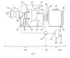
- a circuit according to the first embodiment of the invention is an inverter circuit with a primary side 100 and a secondary side 200.
- rectifier 10 On the primary side 100, rectifier 10 has outputs connected to power factor correction (PFC) stage 12 which are in turn connected across a pair of transistors in series, a high side transistor 14 in series with low side transistor 16.
- PFC power factor correction
- the central node 18 between high and low side transistors 14, 16 is connected to the primary winding 20 of transformer 22 and then through the primary winding 20 to capacitor 24.
- Driver circuit 26 is connected to the gate 28 of the high side transistor 14 and to the gate 30 of the low side transistor 16.
- the secondary winding 32 of transformer 22 is connected through an inductor 34 to the load, a cold cathode fluorescent tube 36.
- the external inductor 34 is omitted, and the secondary winding 32 itself is made lossy.
- a sense coil 38 is arranged to sense the current passing through the cold cathode fluorescent tube 36, the sense coil 38 being connected to controller 40.
- the controller 40 has control inputs 42 and a control output 44 which is connected through optical isolator 46 to an input 48 on the driver 26 in the primary side.
- the primary 100 and secondary 200 sides are accordingly isolated across mains separation 50, with the power being transmitted forward across the mains separation 50 by transformer 22 and feedback transmitted back across the mains separation by optical isolator 46.
- the high and low side transistors 14,16 In use, there are four possible states of the high and low side transistors 14,16. In an idle state (state one), both transistors are switched off. In a second state (state two), the low side transistor 16 is off and the high side transistor 14 on. In a third state (state three), the low side transistor 16 is on and the high side transistor 16 off. A fourth state has both high and low side transistors on, and is to be avoided since this state acts effectively as a short circuit.
- the controller 40 needs to transmit a signal back to the driver 26 indicating which of the three states is required.
- One way of achieving this would be to provide two optical couplers 46 and two one-bit signals across mains separation 50, for example one signal to control the high side transistor 14 and one signal to control the low side transistor 16.
- the inventor has realised that the difficulty and expense of such a solution can be avoided and only a single binary signal (with high and low states) used to control the high and low side transistors 14,16 by defining a memory time, and defining state one (the idle state) to exist after the binary signal has been in one of the high and low states for at least the memory time. If the binary signal has changed within the memory time, then the binary signal defines either state two or state three depending on the state of the binary signal.
- the memory time is a predetermined constant.
- Figure 2 illustrates this; the graph shows the binary signal and the corresponding state of the system, where 1 indicates state one, 2 indicates state two and 3 indicates state three.
- the system starts in idle state (state one) with the binary signal low.
- the binary signal then switches to high, indicating state two, and then low again, indicating state three.
- the binary signal stays low for less time than the memory time, t mem , before going high to indicate state two again.
- the binary signal goes low again, indicating state three. This time, however, the binary signal stays low for more than the memory time t mem and so after the expiry of the memory time t mem the binary signal indicates state one. In this way, a single binary signal with two values can be used to communicate all three required states.
- state one is indicated by the binary signal being in a predetermined one of its two states - in the example low - for at least the memory time. At times when the binary signal is in this predetermined one of its two states - in the example low - for less than the memory time the high and low side transistors are driven in a predetermined one of state two and state three.
- driver 26 The interpretation of the signal by driver 26 is achieved by a memory cell 52 which stores the state of the binary signal input to driver 26 on input 48 for the memory time.
- an ac mains signal is applied to rectifier 10 and this is rectified and passed through PFC stage 12 to supply a voltage of approximately 400V dc across the high and low side transistors 14,16.
- the signal is switched by high and low side transistors 14, 16 under control of driver 26 in turn under the control of controller 40 to supply a switched current through the primary winding 20 of transformer 22 and to induce a current in the secondary winding 32 on the secondary side.
- the currrent drives the load, the cold cathode fluorescent tube 36.
- the current through the load is sensed on sense coil 38 which is used as an input to controller 40 which supplies a binary feedback signal having two states (high and low) back through optical isolator 46 to input 48 of driver 26.
- optical isolator 46 alternative isolation components may be used such as a two-winding transformer.
- Other current sensing components may be used instead of sense coil 38.
- the idle state is indicated by the binary signal being low for the memory time.
- the idle state can be indicated by the binary signal being high for the memory time.
- the memory time is a constant.
- the memory time varies, depending on the length of time the binary signal is held in the other one of the two states from the predetermined state.
- the memory time may depend on the time that the binary signal was previously held high.
- the memory time will be set to be a little longer than the time the binary signal was previously in its high state.
- the system can be switched off by reducing the time of each successive high state in a number of successive cycles to reduce the memory time before finally switching the circuit into the idle state.
- a higher initial value of memory time can be used.
- Figure 3 illustrates the square wave signal output on output node 18 (top graph) and the current in the primary coil 20 in two cases with different t mem , the lower graph having a longer t mem at the time the circuit is finally switched into the idle state.
- the initial state of the inverter (up until time t mem ) has the low side transistor on hence driving an output on the output node 18.
- This drive causes a current through the primary coil 20, so the longer the low side transistor is on the more current builds up in the primary coil 20.
- the high and low side transistors are switched off and the current decays with a "ringing" type oscillation.
- the longer the time period t mem at the moment the inverter is switched off the larger the current that has built up in the primary coil 20 and so the larger the ringing.
- the controller 40 is arranged to switch the inverter into the idle state over a plurality of cycles by reducing the time the binary signal is high over successive cycles to reduce t mem before ending the cycles to switch the inverter into the idle state.
- the value of t mem can be reduced to a lower or minimal value before finally switching the inverter off. In this way, the ringing is reduced.
- FIG. 4 illustrates an alternative embodiment in which, instead of a memory cell 52 integrated into driver 26, the driver 26 includes external circuit components 54 having a time constant corresponding to the memory time is used.
- the driver has a pair of inputs, a first input 56 directly connected to the optical isolator 46, and a second input 58 connected to the first input 56, and hence the optical isolator 46, through diode 60.
- An RC circuit with a resistor 62 and capacitor 64 connects the second input to the low side.
- the driver 26 in this embodiment compares the voltage on the second input 58 with a reference voltage V ref , and whilst the signal on the first input 56 is low but the voltage on the second input 58 is above the reference voltage V ref , the driver drives the transistors in state three with the low side transistor 16 on and the high side transistor 14 off.
- the driver drives the transistors in state one with both the low side transistor 16 and the high side transistor 14 off.
- the time constant of the RC circuit of resistor 62 and capacitor 64 together with the relative sizes of the reference voltage and the signal voltage determine the memory time.
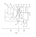
- FIG. 5 illustrates an alternative arrangement using an LLC resonant converter using the same technique as the embodiments above.
- the converter On the secondary side 200 the converter has a pair of secondary windings 70,72 each of which is connected through a respective output diode 74,76 to a first dc voltage output 78.
- the secondary windings are connected together at a centre node 80 connected to a second dc voltage output 82.
- the output voltage is delivered across first and second dc voltage outputs 78, 82.
- the controller 40 is connected to the first and second dc voltage outputs 78, 82.
- Smoothing capacitor 81 is provided across the voltage outputs 78, 82.
- the voltage across the first and second dc voltage outputs is determined and used to generate the feedback signal.
- the embodiments above are half bridge arrangements in which there is a single high side transistor and a single low side transistor.
- the invention is also applicable to a full bridge arrangements as illustrated in Figure 6 .
- the primary winding 20 is connected between first 84 and second 86 primary side output nodes in series with capacitor 87.
- the first primary side output node 84 is connected between a first high side transistor 88 and a first low side transistor 90 and the second primary side output node 86 is connected between a second high side transistor 92 and a second low side transistor 94.
- each of the first and second bridge circuit needs a separate binary control line from the controller 40 on the secondary side 200 and so a first optical isolator 96 is used for a first binary signal to control the first high side transistor and the first low side transistor and a second optical isolator 98 is used for a second binary signal to control the second high side transistor and the second low side transistor.
- each of the first and second binary signals controls the respective transistors in exactly the same way as in the half bridge embodiments above.
- the first and second binary signals will control the respective transistors differently, as appropriate for a full bridge rectifier, so the controller 40 will need to output different control signals.
- the output voltage may now be adjusted by adjusting the phase between the first and second binary signals as is known to those skilled in the art.
- the high and low states of the binary signal can be interchanged, and indeed rearranged; for example, the binary signal being high may correspond to a state with the low side transistor on.
Landscapes
- Engineering & Computer Science (AREA)
- Power Engineering (AREA)
- Inverter Devices (AREA)
- Circuit Arrangements For Discharge Lamps (AREA)
Priority Applications (2)
| Application Number | Priority Date | Filing Date | Title |
|---|---|---|---|
| EP09157852A EP2242172A1 (de) | 2009-04-14 | 2009-04-14 | Wechselrichter mit nur einem 1-Bit Rückkopplungssignal zur Regelung dreier Schaltzustände |
| PCT/IB2010/051591 WO2010119399A2 (en) | 2009-04-14 | 2010-04-13 | Mains separator in an inverter |
Applications Claiming Priority (1)
| Application Number | Priority Date | Filing Date | Title |
|---|---|---|---|
| EP09157852A EP2242172A1 (de) | 2009-04-14 | 2009-04-14 | Wechselrichter mit nur einem 1-Bit Rückkopplungssignal zur Regelung dreier Schaltzustände |
Publications (1)
| Publication Number | Publication Date |
|---|---|
| EP2242172A1 true EP2242172A1 (de) | 2010-10-20 |
Family
ID=41119260
Family Applications (1)
| Application Number | Title | Priority Date | Filing Date |
|---|---|---|---|
| EP09157852A Withdrawn EP2242172A1 (de) | 2009-04-14 | 2009-04-14 | Wechselrichter mit nur einem 1-Bit Rückkopplungssignal zur Regelung dreier Schaltzustände |
Country Status (2)
| Country | Link |
|---|---|
| EP (1) | EP2242172A1 (de) |
| WO (1) | WO2010119399A2 (de) |
Cited By (1)
| Publication number | Priority date | Publication date | Assignee | Title |
|---|---|---|---|---|
| CN102594153A (zh) * | 2012-02-28 | 2012-07-18 | 长城汽车股份有限公司 | 一种车用直流变换器 |
Citations (2)
| Publication number | Priority date | Publication date | Assignee | Title |
|---|---|---|---|---|
| US20060284568A1 (en) | 2005-06-17 | 2006-12-21 | Hon Hai Precision Industry Co., Ltd. | Power supply system for flat panel display devices |
| JP2008178283A (ja) * | 2006-12-22 | 2008-07-31 | Sanken Electric Co Ltd | 交流電源装置及び交流電源装置用集積回路 |
-
2009
- 2009-04-14 EP EP09157852A patent/EP2242172A1/de not_active Withdrawn
-
2010
- 2010-04-13 WO PCT/IB2010/051591 patent/WO2010119399A2/en not_active Ceased
Patent Citations (3)
| Publication number | Priority date | Publication date | Assignee | Title |
|---|---|---|---|---|
| US20060284568A1 (en) | 2005-06-17 | 2006-12-21 | Hon Hai Precision Industry Co., Ltd. | Power supply system for flat panel display devices |
| JP2008178283A (ja) * | 2006-12-22 | 2008-07-31 | Sanken Electric Co Ltd | 交流電源装置及び交流電源装置用集積回路 |
| US20090122581A1 (en) * | 2006-12-22 | 2009-05-14 | Sanken Electric Co., Ltd | Alternating current power supply device and integrated circuit for alternating current power supply device |
Cited By (2)
| Publication number | Priority date | Publication date | Assignee | Title |
|---|---|---|---|---|
| CN102594153A (zh) * | 2012-02-28 | 2012-07-18 | 长城汽车股份有限公司 | 一种车用直流变换器 |
| CN102594153B (zh) * | 2012-02-28 | 2014-06-04 | 长城汽车股份有限公司 | 一种车用直流变换器 |
Also Published As
| Publication number | Publication date |
|---|---|
| WO2010119399A2 (en) | 2010-10-21 |
| WO2010119399A3 (en) | 2010-12-09 |
Similar Documents
| Publication | Publication Date | Title |
|---|---|---|
| US6778415B2 (en) | Controller electrical power circuit supplying energy to a display device | |
| US9048736B2 (en) | Power adaptor with power-saving mechanism | |
| EP2306786A1 (de) | Rückbeleuchtungsanordnung und Anzeigevorrichtung und Fernseher damit | |
| US20090243994A1 (en) | Backlight control device and display apparatus | |
| US20040263095A1 (en) | Backlight inverter for liquid crystal display panel of asynchronous pulse width modulation driving type | |
| TW200426749A (en) | Power supply for an LCD panel | |
| US20080309244A1 (en) | Primary-side driving control circuit for backlight of LCD panel | |
| US20130050280A1 (en) | Display system, control circuit for generating a backlight driving current and method thereof | |
| TW201128612A (en) | LED backlight circuit for LCD panels | |
| WO2020181830A1 (zh) | 显示装置及供电控制方法 | |
| KR101018114B1 (ko) | 액정 표시 장치의 전원 공급 장치 | |
| JP2006024511A (ja) | 放電灯点灯装置 | |
| EP2242172A1 (de) | Wechselrichter mit nur einem 1-Bit Rückkopplungssignal zur Regelung dreier Schaltzustände | |
| KR20090119676A (ko) | 램프 제어시스템 | |
| JP2007059155A (ja) | 冷陰極管点灯装置、該冷陰極管点灯装置に用いられる管電流検出回路、管電流制御方法、及び集積回路 | |
| KR100785161B1 (ko) | 멀티램프모듈 구동시스템 | |
| JP3101783U (ja) | デジタル制御による多光源駆動装置 | |
| US20070205728A1 (en) | Discharge lamp lighting apparatus | |
| JP4025300B2 (ja) | 電源回路の制御器と駆動方法及びエネルギー供給のための電気回路及びその電気回路を備えた表示装置 | |
| KR101048257B1 (ko) | Led 구동 회로 | |
| CN201369871Y (zh) | 背光源驱动系统及电子设备 | |
| US7741790B2 (en) | Backlight system having a lamp current balance and feedback mechanism and related method thereof | |
| TWI403216B (zh) | 光源亮度控制電路及亮度控制方法 | |
| KR100483051B1 (ko) | Lcd 패널용 백라이트 인버터의 트랜스 오동작 검출 회로 | |
| KR100859292B1 (ko) | 다수의 방전관용 램프를 구동하기 위한 다상 인버터 장치 |
Legal Events
| Date | Code | Title | Description |
|---|---|---|---|
| PUAI | Public reference made under article 153(3) epc to a published international application that has entered the european phase |
Free format text: ORIGINAL CODE: 0009012 |
|
| AK | Designated contracting states |
Kind code of ref document: A1 Designated state(s): AT BE BG CH CY CZ DE DK EE ES FI FR GB GR HR HU IE IS IT LI LT LU LV MC MK MT NL NO PL PT RO SE SI SK TR |
|
| 17P | Request for examination filed |
Effective date: 20110420 |
|
| STAA | Information on the status of an ep patent application or granted ep patent |
Free format text: STATUS: THE APPLICATION IS DEEMED TO BE WITHDRAWN |
|
| 18D | Application deemed to be withdrawn |
Effective date: 20121101 |