EP2240003A2 - Beleuchtungsmodul, das Strom kompensieren kann - Google Patents
Beleuchtungsmodul, das Strom kompensieren kann Download PDFInfo
- Publication number
- EP2240003A2 EP2240003A2 EP10002634A EP10002634A EP2240003A2 EP 2240003 A2 EP2240003 A2 EP 2240003A2 EP 10002634 A EP10002634 A EP 10002634A EP 10002634 A EP10002634 A EP 10002634A EP 2240003 A2 EP2240003 A2 EP 2240003A2
- Authority
- EP
- European Patent Office
- Prior art keywords
- unit
- resistor
- illuminating
- illuminating module
- circuit
- Prior art date
- Legal status (The legal status is an assumption and is not a legal conclusion. Google has not performed a legal analysis and makes no representation as to the accuracy of the status listed.)
- Withdrawn
Links
- XUIMIQQOPSSXEZ-UHFFFAOYSA-N Silicon Chemical compound [Si] XUIMIQQOPSSXEZ-UHFFFAOYSA-N 0.000 claims description 12
- 229910052710 silicon Inorganic materials 0.000 claims description 12
- 239000010703 silicon Substances 0.000 claims description 12
- 238000010586 diagram Methods 0.000 description 8
- 230000007423 decrease Effects 0.000 description 5
- 230000002159 abnormal effect Effects 0.000 description 2
- 230000000694 effects Effects 0.000 description 2
- 238000005286 illumination Methods 0.000 description 2
- 230000004048 modification Effects 0.000 description 1
- 238000012986 modification Methods 0.000 description 1
- 230000001131 transforming effect Effects 0.000 description 1
Images
Classifications
-
- H—ELECTRICITY
- H05—ELECTRIC TECHNIQUES NOT OTHERWISE PROVIDED FOR
- H05B—ELECTRIC HEATING; ELECTRIC LIGHT SOURCES NOT OTHERWISE PROVIDED FOR; CIRCUIT ARRANGEMENTS FOR ELECTRIC LIGHT SOURCES, IN GENERAL
- H05B41/00—Circuit arrangements or apparatus for igniting or operating discharge lamps
- H05B41/14—Circuit arrangements
- H05B41/26—Circuit arrangements in which the lamp is fed by power derived from DC by means of a converter, e.g. by high-voltage DC
- H05B41/28—Circuit arrangements in which the lamp is fed by power derived from DC by means of a converter, e.g. by high-voltage DC using static converters
- H05B41/282—Circuit arrangements in which the lamp is fed by power derived from DC by means of a converter, e.g. by high-voltage DC using static converters with semiconductor devices
- H05B41/2825—Circuit arrangements in which the lamp is fed by power derived from DC by means of a converter, e.g. by high-voltage DC using static converters with semiconductor devices by means of a bridge converter in the final stage
- H05B41/2828—Circuit arrangements in which the lamp is fed by power derived from DC by means of a converter, e.g. by high-voltage DC using static converters with semiconductor devices by means of a bridge converter in the final stage using control circuits for the switching elements
Definitions
- the invention relates to an illuminating module capable of compensating current, and particularly, the invention relates to an illuminating module which can judge if the current in the silicon controlled rectifier of the light modulating circuit is insufficient and then further compensate current.
- the dimmer is used for adjusting the illumination of the lamp according to the requirement of the user.
- the flicker occurs when the current is less then a specific value.
- the life of the CCFL would be reduced when the flicker occurs frequently.
- the invention is to provide an illuminating module capable of compensating current which can judge if the current in the silicon controlled rectifier of the light modulating circuit is insufficient and then further compensate current for the light modulating circuit, so that the flicker of the tube, caused by the abnormal bouncing of the silicon controlled rectifier generated by the insufficiency of current, could be avoided.
- a scope of the invention is to provide an illuminating module capable of compensating current, and the illuminating module can tuning the light with a light modulating circuit.
- the illuminating module includes an illuminating unit and a compensating circuit.
- the illuminating unit has a potential source, a load impedance, and a level unit.
- the level unit has a level potential which changes with the light modulating circuit.
- the compensating circuit includes a first resistor, a first switch, and a judging unit.
- the first resistor is coupled to the potential source.
- the first switch is coupled to the first resistor and the illuminating unit.
- the judging unit is coupled to the level unit and the first switch. When the level potential is less than a predetermined potential, the judging unit makes the first switch to be at the conducting state to parallel connect the first resistor and the load impedance.
- the illuminating module capable of compensating current of the invention can detect the insufficiency of current supplied to the silicon controlled rectifier by the light modulating circuit, and then further compensate current for the light modulating circuit. Therefore, the flicker generated by the repeatedly on and off states of the silicon controlled rectifier can be avoid, wherein the rectifier would be turned off by the insufficiency of current and turned on by the triggering of the potential.
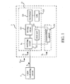
- FIG. 1 is a function block diagram illustrating an illuminating module 3 capable of compensating current according to an embodiment of the invention.
- the illuminating module 3 is connected to a light modulation circuit 4, and the illuminating module 3 can tune the light with the light modulating circuit 4. That is to say, the light modulating circuit 4 can tune the light emitting from the illuminating module 3 to control the illumination.
- the illuminating module 3 includes an illuminating unit 32 and a compensating circuit 34.
- the illuminating module 3 has an impedance Z total .
- the illuminating unit 32 has an impedance Z 1
- the compensating circuit 34 has an impedance Z 2 .
- the illuminating unit 32 includes the load impedance Z 1 , a potential node N 1 , a rectifying circuit 322, a driving circuit 323, a transformer 324, a tube 325, and a level unit 326.
- the rectifying circuit 322 is coupled to the potential node N 1 , the driving circuit 323, and the level unit 326.
- the driving circuit 323 is coupled to the transformer 324.
- the transformer 324 is coupled to the tube 325.
- the driving circuit 323 can be used for generating a Pulse Width Modulation (PWM) signal.
- PWM Pulse Width Modulation
- the transformer 324 can be used for transforming the PWM signal to a sinusoidal wave.
- the tube 325 can include a Cold Cathode Fluorescence Lamp
- CCFL shape, amount, and length of the CCFL included by tube 325 are not limited to a specific type but decided according to the request of the user.
- the compensating circuit 34 is coupled to the rectifying circuit 322 and the level unit 326.
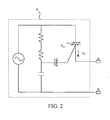
- FIG. 2 is a schematic diagram illustrating the internal circuit of the light modulating circuit 4 in FIG. 1 .
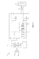
- FIG. 3 is a schematic diagram illustrating the internal circuit of the illuminating unit 32 in FIG. 1 .
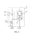
- FIG. 4 is a schematic diagram illustrating the internal circuit of the compensating circuit 34 in FIG. 1 .
- the light modulating circuit 4 includes an AC silicon controlled rectifier T 41 , and the AC silicon controlled rectifier T 41 has a current I 41 thereon.
- the points A and B in FIG. 2 are respectively connected to the points A and B in FIG. 3 .
- the AC silicon controlled rectifier T 41 can be used for changing a conduction angle of the input to the illuminating unit 32.
- the rectifying circuit 322 of the illuminating unit 32 can be, but not limited to, a bridge rectifier.
- the rectifying circuit 322 has a current I 31 , and the current I 31 is substantially the same as the current I 31 .
- the level unit 326 can be, but not limited to, a resistor.
- the compensating circuit 34 includes a first switch 341, a first resistor 342, and a judging unit 343.
- the first switch 341 is coupled to the first resistor 342.
- the first switch 341 can be, but not limited to, a MOSFET.
- the first resistor 342 is coupled to the potential node N 1 .
- the first resistor 342 can include at least one resistor parallel connected or series connected to each other, but it is not a limitation. The purpose to parallel connect or series connect the at least one resistor included by the first resistor 342 is to disperse the thermal energy generated by the at least one resistor.
- the judging unit 343 is connected to the points C and D in
- the judging unit 343 is coupled to the level unit 326 and the first switch 341.
- the judging unit 343 includes a first MOSFET 3431 and a second resistor 3432.
- the first MOSFET 3431 is electrically connected to the level unit 326 and the second resistor 3432.
- the second resistor 3432 is electrically connected to a reference power source V 1 .
- the reference power source V 1 can be, but not limited to, 15 volts.
- the situation that the current I 31 is greater than a predetermined value would be discussed firstly.
- the current I 31 flowing through the level unit 326 generates a level potential VL.
- the level potential VL makes the first switch 341 to keep the off state.
- the first switch 341 is at the off state; the first resistor has no influence and effect to the whole circuit.
- the impedance Z total of the illuminating module 3 is equal to the impedance Z 1 of the illuminating unit 32.
- the situation that the current I 31 is less than a predetermined value would be discussed.
- the current I 31 is influenced by the conduction angle of the light modulating circuit 4 to be less than 0.075A (it should be noted that the predetermined value is not limited to 0.075A), and then the level potential VL decreases.
- the level potential VL decreases, the potential across the first MOSFET 3431 would decrease too.
- the first MOSFET 3431 would be turned off if the level potential VL decreases to the condition of disabling the first MOSFET 3431 from keeping the conducting state.
- the first MOSFET is turn off, the first switch 341 would be at the conducting state. In other words, the first switch 341 would be turned on. Therefore, the first resistor 342 is parallel connected to the potential node N 1 .
- the effect that the first resistor 342 is parallel connected to the potential nodes N 1 can be regarded as that the compensating circuit 34 provides the impedance Z 2 . Therefore, the load impedance Z 1 of the illuminating unit 32 would be parallel connected to the compensating impedance Z 2 .
- the impedance Z total is defined as the total impedance of the illuminating module 3, so that the impedance Z total is equal to the load impedance Z 1 parallel connected to the compensating impedance Z 2 at this situation.
- Ohm's law when the potential is fixed, the decrease of the impedance causes the increase of the current, so that it is obvious that the current I 31 would increase.
- the increase of current I 31 enables the silicon controlled rectifier T 41 to keep at the on state, and then the bouncing and the flicker of the tube would be avoided.
- the illuminating module capable of compensating current of the invention can judge if the current in the silicon controlled rectifier of the light modulating circuit is insufficient and then further compensate current. Therefore, the abnormal actions of the silicon controlled rectifier caused by the insufficiency of current could be avoided.
Landscapes
- Circuit Arrangement For Electric Light Sources In General (AREA)
Applications Claiming Priority (1)
| Application Number | Priority Date | Filing Date | Title |
|---|---|---|---|
| TW98111509A TW201038135A (en) | 2009-04-07 | 2009-04-07 | Illuminating module capable of compensating current |
Publications (1)
| Publication Number | Publication Date |
|---|---|
| EP2240003A2 true EP2240003A2 (de) | 2010-10-13 |
Family
ID=42341380
Family Applications (1)
| Application Number | Title | Priority Date | Filing Date |
|---|---|---|---|
| EP10002634A Withdrawn EP2240003A2 (de) | 2009-04-07 | 2010-03-12 | Beleuchtungsmodul, das Strom kompensieren kann |
Country Status (2)
| Country | Link |
|---|---|
| EP (1) | EP2240003A2 (de) |
| TW (1) | TW201038135A (de) |
-
2009
- 2009-04-07 TW TW98111509A patent/TW201038135A/zh unknown
-
2010
- 2010-03-12 EP EP10002634A patent/EP2240003A2/de not_active Withdrawn
Non-Patent Citations (1)
| Title |
|---|
| None |
Also Published As
| Publication number | Publication date |
|---|---|
| TW201038135A (en) | 2010-10-16 |
Similar Documents
| Publication | Publication Date | Title |
|---|---|---|
| US8339053B2 (en) | LED dimming apparatus | |
| US9560704B2 (en) | LED driving device and LED lighting apparatus | |
| US8120280B2 (en) | Circuits and methods for controlling a light source | |
| US9225254B2 (en) | Supply circuit having at least one switching unit coupled between a bridge circuit and an associated load circuit | |
| US8106596B2 (en) | Light source driving circuit | |
| US20080054817A1 (en) | Driving apparatus of light source | |
| JP2004296205A (ja) | Led調光点灯装置及び照明器具 | |
| US9277608B2 (en) | Circuit for operating parallel light emitting diode strings | |
| TW201505484A (zh) | 發光二極體驅動裝置及應用其之發光二極體照明系統 | |
| US20100103091A1 (en) | Light emitting diode array, driving system thereof and liquid crystal display using the same | |
| JP4686434B2 (ja) | アクティブ型電流調整回路及びその発光構造 | |
| CN101236726A (zh) | 液晶显示器、调光电路及其方法 | |
| US8198825B2 (en) | Illuminating module capable of compensating current | |
| US11343891B2 (en) | LED system for vehicle lighting having high efficiency and high reliability | |
| EP2240003A2 (de) | Beleuchtungsmodul, das Strom kompensieren kann | |
| JP2014131420A (ja) | 電源装置 | |
| JP2013135207A (ja) | 発光ダイオード駆動装置 | |
| KR101007034B1 (ko) | 발광 다이오드용 전원 공급 장치 | |
| KR101007035B1 (ko) | 발광 다이오드용 전원 공급 장치 | |
| US8686661B2 (en) | LED dimming method and LED dimming system | |
| JP2009054998A (ja) | 駆動装置 | |
| KR20100072733A (ko) | 발광 다이오드용 전원 공급 장치 | |
| KR20100000362U (ko) | 엘이디 조명장치용 디밍회로 | |
| KR20130001640A (ko) | 발광 다이오드 구동회로 | |
| KR100968925B1 (ko) | 발광 다이오드용 전원 공급 장치 |
Legal Events
| Date | Code | Title | Description |
|---|---|---|---|
| PUAI | Public reference made under article 153(3) epc to a published international application that has entered the european phase |
Free format text: ORIGINAL CODE: 0009012 |
|
| 17P | Request for examination filed |
Effective date: 20100312 |
|
| AK | Designated contracting states |
Kind code of ref document: A2 Designated state(s): AT BE BG CH CY CZ DE DK EE ES FI FR GB GR HR HU IE IS IT LI LT LU LV MC MK MT NL NO PL PT RO SE SI SK SM TR |
|
| AX | Request for extension of the european patent |
Extension state: AL BA ME RS |
|
| STAA | Information on the status of an ep patent application or granted ep patent |
Free format text: STATUS: THE APPLICATION HAS BEEN WITHDRAWN |
|
| 18W | Application withdrawn |
Effective date: 20120206 |