EP2239812B1 - Transmission apparatus and communication system - Google Patents
Transmission apparatus and communication system Download PDFInfo
- Publication number
- EP2239812B1 EP2239812B1 EP10002629A EP10002629A EP2239812B1 EP 2239812 B1 EP2239812 B1 EP 2239812B1 EP 10002629 A EP10002629 A EP 10002629A EP 10002629 A EP10002629 A EP 10002629A EP 2239812 B1 EP2239812 B1 EP 2239812B1
- Authority
- EP
- European Patent Office
- Prior art keywords
- signal
- transmission
- block
- phase
- transmission signal
- Prior art date
- Legal status (The legal status is an assumption and is not a legal conclusion. Google has not performed a legal analysis and makes no representation as to the accuracy of the status listed.)
- Not-in-force
Links
Images


Classifications
-
- H—ELECTRICITY
- H01—ELECTRIC ELEMENTS
- H01P—WAVEGUIDES; RESONATORS, LINES, OR OTHER DEVICES OF THE WAVEGUIDE TYPE
- H01P1/00—Auxiliary devices
- H01P1/18—Phase-shifters
- H01P1/182—Waveguide phase-shifters
-
- H—ELECTRICITY
- H04—ELECTRIC COMMUNICATION TECHNIQUE
- H04L—TRANSMISSION OF DIGITAL INFORMATION, e.g. TELEGRAPHIC COMMUNICATION
- H04L27/00—Modulated-carrier systems
- H04L27/32—Carrier systems characterised by combinations of two or more of the types covered by groups H04L27/02, H04L27/10, H04L27/18 or H04L27/26
- H04L27/34—Amplitude- and phase-modulated carrier systems, e.g. quadrature-amplitude modulated carrier systems
- H04L27/36—Modulator circuits; Transmitter circuits
Definitions
- Patent Document 1 discloses a transmitting device having a compensating circuit configured, in consideration of the accuracy of an quadrature modulating circuit, to suppress a carrier wave leak below a desired value by increasing or decreasing a direct current bias so that a voltage detected by a wave detector goes below a predetermined level.
- Patent Document 2 discloses a wireless communication apparatus configured to switch to the BPSK (Binary Phase Shift Keying) scheme if the accuracy is poor and IQ orthogonality is unnecessary and switch to the QPSK scheme if the accuracy is good, thereby assuring the maintenance of the transmission channel rather than the maintenance of IQ quadrature accuracy.
- BPSK Binary Phase Shift Keying
- the inventions disclosed in the above-mentioned Patent Documents 1 and 2 involve the following problems if the high-speed transmission based on IQ quadrature axis is achieved by using a 90-degree phase shift or the like.
- the invention disclosed in Patent Document 1 desires the installation of a compensating circuit including a computation block, a wave detection block and so on in addition to a transmission path including a signal modulation block, a signal mixer and so on that is inherent to the transmitter. This prevents the circuit scale of the transmitter from being made smaller in size, which leads to an increased cost.
- the invention disclosed in the Patent Document 2 it is obvious that the transfer rate drops at application of BPSK modulation, so that stable high-speed transmission may not be expected.
- the embodiments of the present invention addresses the above-identified and other problems associated with related-art methods and apparatuses and solves the addressed problems by providing a transmission apparatus using a waveguide and a communication system composed thereof configured to realize precision and high-speed transmission while achieving circuit simplification by removing the use of the 90-degree phase shifter for orthogonalizing I-axis and Q-axis, the quadrature oscillator, and so on.
- a communication systeme In carrying out the invention and according to another mode thereof, there is provided a communication systeme.
- This communication system has a transmission apparatus as defined in claim 1 and a reception apparatus configured to receive the first transmission signal and the second transmission signal transmitted via the waveguide and demodulate the received first transmission signal and the received second transmission signal to obtain reception signals on the basis of a carrier-wave signal having a predetermined frequency.
- a waveguide is arranged in a state where a first input point and a second input point are shifted from each other by a distance that provides a phase difference between a first transmission signal and a second transmission signal.
- This novel configuration can realizes IQ quadrature transmission without using a quadrature oscillator and a 90-degree phase shifter. As a result, the circuit scale and cost of the transmission apparatus can be significantly reduced.
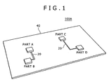
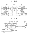
- a high-frequency transmission system 100A associated with the embodiments of the present invention is one exemplary communication system that is capable of the high-speed transmission of a millimeter-wave transmission signal of 30 GHz to 300 GHz, for example.
- This high-frequency transmission system 100A is configured by a part A, a part B, a part C, and a part D mounted on a substrate 40 and a waveguide 20 interconnecting the parts A, B, C, and D.
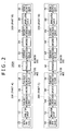
- the high-frequency transmission system 100A has the transmission apparatus 200, the reception apparatus 300, and the waveguide 20 for interconnecting these apparatuses.
- the transmission apparatus 200 has a signal input block 10, a modulation circuit 12, a frequency conversion circuit 14, an amplifier 16, and a connection circuit 18 for connecting the transmission apparatus 200 with a substrate.
- the reception apparatus 300 has a connection circuit 22 for connecting the reception apparatus 300 with the substrate, an amplifier 24, a frequency conversion block 26, a demodulation circuit 28, and a signal output block 30.
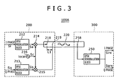
- BPSK modulation blocks 212 and 213 correspond to the modulation circuit 12 shown in FIG. 12
- a carrier-wave signal generation block 216 and mixers 214 and 215 correspond to the frequency conversion circuit 14 shown in FIG. 2
- input points 218 and 219 correspond to the connection circuit 18 shown in FIG. 2
- an output point 258 corresponds to the connection circuit 22 shown in FIG. 2
- a QPSK demodulation block 250 corresponds to the demodulation circuit 28 shown in FIG. 2 .
- the mixer 214 multiplies modulation signal Sa generated by the BPSK modulation block 212 by carrier-wave signal Sc generated by the carrier-wave signal generation block 216 to frequency-convert (up-convert) modulation signal Sa, supplying frequency-converted modulation signal Sa to the input point 218.
- baseband signal Si is one example of a first signal
- modulation signal Sa is one example of a first transmission signal.
- the input point 218 is one example of a first input point and the BPSK modulation block 212 and the mixer 214 are one example of a first transmission block.
- Baseband signal Sq allocated to Q-phase is supplied to the BPSK modulation block 213.
- the BPSK modulation block 213 generates modulation signal Sb by executing BPSK modulation (mapping) on this baseband signal in accordance with allocated bits and supplies the modulated signal Sb to the mixer 215.
- the carrier-wave signal generation block 216 generates carrier-wave signal Sc having a predetermined frequency and supplies the generated signal to the mixer 215.
- the mixer 215 multiplies modulation signal Sb generated by the BPSK modulation block 213 by carrier-wave signal Sc to frequency-convert (up-convert) modulation signal Sb, supplying frequency-converted modulation signal Sb to the input point 219.
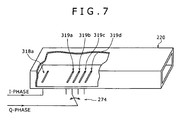
- the input points 218 and 219 are arranged at one end of the waveguide 220.
- the input point 218 and 219 each have a dipole antenna, loop antenna, or a small-size aperture connection element (or a slit antenna), for example.
- the input point 218 and 219 are shifted from each other by distance L1 that satisfies a relationship of equation (2) below for giving a predetermined phase difference between modulation signal Sa and modulation signal Sb in the carrier direction of the waveguide 220.
- L ⁇ 1 1 / 4 + N ⁇
- modulation signal Sa transmitted from the input point 218 and modulation signal Sb transmitted from the input point 219 are shifted from each other at least 90 degrees on complex plane.
- shifting distance L1 between the input point 218 and the input point 219 by (1/4+N) ⁇ enables to orthogonalize the phases of modulation signals Sa and Sb without the use of a 90-degree phase shifter as practiced in related-art technologies.
- This state when observed at one point (the output point 258) for example) on the waveguide 220, is equal to the relationship between sine wave and cosine wave, making it equivalent to a state in which a QPSK-modulated signal has arrived, so to speak.
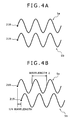
- FIG. 4A shows a phase relationship between modulation signals Sa and Sb before phase shifting.
- the waveguide 220 has an elongated housing that partitioned by a conductive member and is mounted between the transmission apparatus 200 and the reception apparatus 300 mounted on the substrate 40.
- a dielectric material having a predetermined specific inductive capacity such as air or epoxy resin (the same material as the substrate 40), for example, is encapsulated.
- a substrate having a relatively large transmission loss in millimeter band and therefore considered not suitable for millimeter wave transmission is used; namely, such a substrate covered with copper foils on both sides of the substrate with a glass epoxy resin used as insulation base having a dielectric tangent (tan ⁇ ) of 0.01 or more.
- the output point 258 is arranged on the other end of the waveguide 220 and has a dipole antenna, loop antenna, or a small-size aperture connection element (or a slit antenna), for example, as will be described later.
- the output point 258 receives modulation signals Sa and Sb transmitted through the waveguide 220 and supplies the received signals to the QPSK demodulation block 250.
- the QPSK demodulation block 250 executes QPSK modulation on the mutually orthogonal demodulation signals Sa and Sb received from the output point 258 to get baseband signal Sirx based on modulation signal Sa and baseband signal Sqrx based on modulation signal Sb.
- a variation to the first embodiment uses a reception apparatus 300 of a high-frequency transmission system 100B in a different configuration from that of the reception apparatus 300 of the high-frequency transmission system 100A described with reference to the above-mentioned first embodiment. It should be noted that components of this variation common to those of the above-mentioned high-frequency transmission system 100A of the first embodiment are denoted by the same reference codes and skipped in detail description.
- the reception apparatus 300 has output points 260 and 261, mixers 254 and 255, and BPSK demodulation blocks 252 and 253.
- the output point 261 is arranged on one end of a waveguide 220.
- the output point 261 has a dipole antenna, for example.
- the output point 261 receives modulation signal Sa transmitted through the waveguide 220 and supplies the received signal to the mixer 254.
- a carrier wave signal generation block 256 generates carrier-wave signal Scrx and supplies the generated signal to the mixer 254.
- the mixer 254 multiplies modulation signal Sa by carrier-wave signal Scrx to frequency-convert (down-convert) modulation signal Sa, supplying resultant frequency-converted modulation signal Sa to the BPSK demodulation block 252.
- the BPSK demodulation block 252 demodulates (or maps) modulation signal Sa to obtain baseband signal Sirx.
- the output point 260 is arranged on the other end of the waveguide 220 and has a dipole antenna for example. Also, the output point 260 is arranged at a position shifted from the output point 261 by distance L1 that satisfies the relationship of equation (2) above.
- modulation signal Sb transmitted through the waveguide 220 can be received with a shift from modulation signal Sb by (1/4+N) ⁇ .
- Received modulation signal Sa is supplied to the mixer 255.
- the mixer 255 multiplies modulation signal Sb received through the waveguide 220 by carrier-wave signal Scrx to frequency-convert (down-convert) modulation signal Sb, supplying resultant frequency-converted modulation signal Sa to the BPSK demodulation block 253.
- the BPSK demodulation block 253 demodulates (or maps) modulation signal Sb to obtain baseband signal Sqrx.
- configuring the reception apparatus 300 like the transmission apparatus 200 can obtain substantially the same effects as those of the first embodiment mentioned above.
- a phase difference between the first modulation signal Sa and the second modulation signal Sb can be set to 90 degrees to realize IQ quadrature transmission without use of a quadrature oscillator or a 90-degree phase shifter, consequently reducing the circuit scale and cost of the transmission apparatus 200.
- An exemplary high-frequency transmission system having a phase calibration function having a phase calibration function:
- a high-frequency transmission system 100C having a calibration function of adjusting a phase difference between modulation signal Sa of I-phase and modulation signal Sb of Q-phase to 90 degrees is described. It should be noted that the high-frequency transmission system 100C is configured by adding this calibration function to the high-frequency transmission system 100A described above, so that the description of components and operations similar to those of the high-frequency transmission system 100A will be skipped.
- an input point 218 of I-phase has an antenna member 218a of dipole type for example having a predetermined length based on wavelength ⁇ of a millimeter-wave signal for example.
- This antenna member 218a is connected to one end of a waveguide 220, thereby radiating modulation signal Sat for testing outputted from a mixer 254 into the waveguide 220.
- the input point 219 of Q-phase has four antenna members 291a through 219d of dipole type for example having a predetermined length based on wavelength ⁇ of a millimeter-wave signal for example. These antenna members are spaced from each other to be connected to one end of the waveguide 220. Any one of these antenna members 219a through 219d is electrically connected to a switch block 274 according to switching, receiving modulation signal Sat for testing radiated from the antenna member 218a in the calibration mode. It should be noted that, in the above-mentioned example, the antenna is configured by four antenna members 219a through 219d; it is also practicable to configure the antenna by two antenna members or five antenna members. As the number of antenna members increases, the finer the phase difference can be adjusted.
- the antenna member 219b for example is connected at a position that is shifted from the antenna member 218a of I-phase by (1/4+N) ⁇ and other antenna members 219a, 219c, and 219d are connected at positions in the proximity of the antenna member 219b.
- Positional (phase shift) information of the antenna member 219a through 219d is stored in a position rotational amount calculation block 270 to be described later. On the basis of a calculated shift and the positional information of the antenna members 219a through 219d, the optimum antenna members 219a to 219d can be selected.
- the antenna members 219a through 219d are of dipole type; however, it is also practicable to use antenna members of slit type.
- slit antenna 318a is formed on the bottom of one end of the waveguide 220 in the short direction thereof.
- the slit antennas 319a through 319d are formed on the bottom of one end of the waveguide 220 along the short direction with predetermined intervals between the antennas.
- any one of the slit antennas 319a through 319d (the slit antenna 319b for example) is formed at a position shifted from the slit antenna 318a by (1/4+N) ⁇ .
- the other slit antennas 319a, 319c, and 319d are formed at positions in the proximity of the slit antenna 319b.
- Such a configuration can also execute fine adjustment of the phase difference between modulation signal Sa and modulation signal Sb.
- the BPSK modulation block 212 of the I-phase side executes BPSK modulation in accordance with allocated baseband signal Sit for testing (bit) to generate modulation signal Sat for testing, which is supplied to the mixer 214.
- the carrier-wave signal generation block 216 generates carrier-wave signal Sct and supplies the generated signal to the mixer 214.
- the mixer 214 multiplies modulation signal Sat generated by the BPSK modulation block 212 by carrier-wave signal Sct to frequency-convert (up-convert) modulation signal Sat, supplying resultant frequency-converted modulation signal Sat to the input point 218.
- Modulation signal Sat supplied to the input point 218 is transmitted into the waveguide 220 via the antenna member.
- any one of the antenna members 219a through 219d arranged on the input point 219 also functions as an antenna member for receiving modulation signal Sat for testing in the calibration mode and receives modulation signal Sat transmitted from the input point 218, supplying the received signal to the mixer 215. It is supposed here that distance L1 between the input point 218 and the input point 219 be set to (1/4+N) ⁇ as described above.
- the mixer 215 multiplies modulation signal Sat received at the antenna member of the input point 219 by carrier-wave signal Sct generated by the carrier-wave signal generation block 216 to frequency-convert (down-convert) modulation signal Sat, thereby obtaining reception signal Sarx.
- Frequency-converted reception signal Sarx is supplied to the position rotational amount calculation block 270 via the switch block 272.
- the switch block 272 is switched to the terminal b side by the position rotational amount calculation block 270 and a control block, not shown.
- the position rotational amount calculation block 270 is one example of a control block and determines whether the phase difference between reception signal Sarx for testing outputted from the mixer 215 and reference signal St is 90 degrees (1/4+N) ⁇ . This is because the phase difference between the input point 218 and the input point 219 is set to (1/4+N) ⁇ , the phase difference between reference signal St and reception signal Sarx is theoretically 90 degrees.
- carrier-wave signal Sct supplied from the carrier-wave signal generation block 216 or modulation signal Sat before being converted by the BPSK modulation block 212 and transmitted from the input point 218 that are stored beforehand is used.
- the position rotational amount calculation block 270 calculates a phase rotational amount, to be more specific, a shift in the phase of reception signal Sarx with reference to the 90 degrees. Then, the position rotational amount calculation block 270 selects one of the antenna members 219a through 219d on the basis of the calculated shift and generates a switching signal in accordance with the selection, supplying the generated switching signal to the switch block 274.
- An exemplary high-frequency transmission system having a phase calibration function having a phase calibration function:
- a carrier-wave signal generation block 216 of a high-frequency transmission system 100D generates carrier-wave signal Sci for testing having a predetermined frequency.
- Carrier-wave signal Sci for testing generated by the carrier-wave signal generation block 216 is radiated from an antenna member 218a of an input point 218 into a waveguide 220.
- An antenna member 219a of an input point 219 receives carrier-wave signal Sci for testing radiated from the antenna member 218a of the input point 218 and supplies the received signal to a mixer 215.
- the carrier wave signal generation block 216 generates carrier-wave signal Scq for testing having a predetermined frequency and supplies the generated signal to the mixer 215.
- carrier-wave signal Sci for testing and carrier-wave signal Scq are supposed to be set to a same frequency.
- the mixer 215 multiplies carrier-wave signal Sci for testing by carrier-wave signal Scq and supplies resultant output signal Smx to a frequency analysis block 280.
- the frequency analysis block 280 determines that distance L1 between the input points 218 and 219 is (1/4+N) ⁇ and maintains the current set antenna member 219a to 219d. On the other hand, if the frequency of output signal Smx is found to be not two times as high, the frequency analysis block 280 determines that distance between the input points 218 and 219 is not (1/4+N) ⁇ and switches a switch block 587 to any one of the input point 219a through 219d shown in FIG. 6 .
- the frequency analysis block 280 selects any one of the antenna members 219a through 219d that provides the a frequency component two times as high as carrier-wave signals Sci and Scq, setting distance L1 between the input points 218 and 219 to (1/4+N) ⁇ . Consequently, the phase of modulation signal Sa transmitted from the antenna member 218a of the input point 219 and modulation signal Sb transmitted from the antenna member 219A of the input point 219 can be orthogonalized.
- An exemplary high-frequency transmission system having an amplitude calibration function having an amplitude calibration function:
- a technique that adjusts an amplitude value in addition to a phase difference between signals transmitted from the antenna members 218a and 219A of the input points 218 and 219 in the calibration mode. It should be noted that the operations to be executed until the transmission of a modulation signal from the input point 218 of the I-phase side are substantially the same as those of the second embodiment described above, so that the description of these operations will be skipped.
- an antenna member 219A of an input point 219 of a high-frequency transmission system 100E functions also as an antenna member for receiving modulation signal Sat in the calibration mode, thereby receiving modulation signal Sat transmitted from an antenna member 218a of an input point 218.
- Modulation signal Sat received by the antenna member 218a is supplied to a mixer 215.
- distance L1 between the input points 218 and 219 be set to (1/4+N) ⁇ as described above.
- the mixer 215 multiplies modulation signal Sat received from the antenna member 219A of the input point 219 by carrier-wave signal Sc generated by a carrier wave signal generation block 216 to frequency-convert modulation signal Sat, thereby obtaining reception signal Sarx.
- Frequency-converted reception signal Sarx is supplied to an amplitude value measurement block 370 via a switch block 276 set to the terminal d side.
- the amplitude value measurement block 370 measures an amplitude value of reception signal Sarx outputted from the mixer 215 to calculate a difference between amplitude values of measured reception signal Sarx, carrier-wave signal Sct supplied from the carrier wave signal generation block 216, and modulation signal Sat before attenuation stored in memory. Then, the amplitude value measurement block 370 generates a control signal based on this amplitude difference to supply the generated control signal to an amplitude value control block 378.
- the amplitude value control block 378 executes amplitude control such that an amplitude value of modulation signal Sat received at the antenna member 219A of the input point 219 matches an amplitude value of modulation signal Sat before attenuation and carrier-wave signal Sct. For example, if received modulation signal Sat has been attenuated, amplitude control is executed so as to raise the amplitude value thereof. Amplitude-controlled reception signal Sarx for testing is supplied to a position rotational amount calculation block 270 via the switch block 276 set to the terminal b side.
- the position rotational amount calculation block 270 executes a phase calibration as described above, thereby selecting the optimum one of the antenna members 219a through 219d.
- an amplitude value control block 380 on the I-phase side and the amplitude value control block 378 on the Q-phase side are used also as amplifiers for amplifying modulation signals Sa and Sb in the normal communication mode.
- measuring the amplitude value of reception signal Sarx for testing in the calibration mode allows the calculation of an attenuation ratio of the amplitude value of modulation signal Sat influenced by the waveguide 220 between the input points 218 and 219. Consequently, an error in the amplitude direction can be corrected for more correct phase calibration.
- An exemplary high-frequency transmission system having a phase calibration function having a phase calibration function:
- a phase calibration is executed by adjusting a phase difference between signals of I-phase and Q-phase by use of a dielectric material that varies dielectric constant by the application of electricity or optical energy rather than by the switching between the above-mentioned two or more antenna members 219a through 219d.
- a liquid crystal as a dielectric material having variable dielectric constant is described.
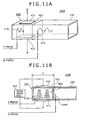
- a phase control block 400 is arranged at the transmission side end of a waveguide 220, phase control block 400 being configured to control a phase difference between two signals by adjusting distance L between input points 218 and 219.
- the phase control block 400 has a housing 402, a liquid crystal layer 406 encapsulated in the housing 402, electrodes 410 and 412 arranged on the upper surface and the lower surface, respectively, of the housing 402, and a voltage control block 414 for applying a predetermined voltage to the electrodes 410 and 412.
- nematic liquid crystal for example is suitably used for the liquid crystal layer 406 . It was clarified that specific inductive capacity ⁇ of nematic liquid crystal is various from 3.0 to the 3.5 in accordance with an applied voltage also in a millimeter band such as 60 GHz. Hence, encapsulating this liquid crystal layer 406 in the waveguide 220 allows the fine adjustment of waveforms while a voltage is applied.
- the voltage control block 414 is connected to the position rotational amount calculation block 270 shown in FIG. 8 , and calculates an applied voltage on the basis of a rotational amount (or a shift) calculated by the position rotational amount calculation block 270, applying the calculated applied voltage to the electrodes 410 and 412. Consequently, the transmissivity of each signal that passes the liquid crystal layer 406 in accordance with an applied voltage value.
- An antenna member 218X of the input point 218 is connected to a terminal block opposite to the waveguide 220 in the housing 402, thereby radiating modulation signal Sa into the waveguide 220 via the liquid crystal layer 406.
- An antenna member 219Y of the input point 219 is connected to a terminal block on the phase control block 400 side in the waveguide 220 outside the housing 402, thereby radiating modulation signal Sb into the waveguide 220.
- distance L between the input points 218X and 219Y is slightly shifted from (1/4+N) ⁇ .
- a signal allocated to I-phase is radiated from the antenna member 218X of the input point 218 into the liquid crystal layer 406 given by specific inductive capacity ⁇ .
- the voltage control block 414 electrically controls an applied voltage to vary the dielectric constant of the liquid crystal layer 406, thereby varying the transmissivity of a signal that passes the liquid crystal layer 406.
- dielectric constants vary include matters using magnetic energy and optical energy and matters using thermal energy and mechanical energy in addition to the liquid crystal layer 406. Therefore it can be easily conceptualize for those skilled in the art to apply these matters to the systems embodied in the present invention.
- One example of varying dielectric constant by use of magnetic energy or optical energy is a matter configured by quantum paraelectrics (such as SrTiO 3 , CaTioO 3 , KTaO 3 , for example) as disclosed in Japanese Patent Laid-open No. 2003-209266 .
- thermal energy is fluorinated ferroelectric polymer, for instance.
- the dielectric constant can be varied by varying the temperature of fluorinated dielectric constant by use of a heat sink.
- mechanical energy is lithium niobate, for instance.
- the dielectric constant can be varied by use of pressure application by fastening a fastening member, such as a screw, onto lithium niobate.
- An exemplary high-frequency transmission system having a phase calibration function having a phase calibration function:
- phase calibration is executed not by switching between the two or more antenna members 219a through 219d described above, but by adjusting a phase difference between the signals of I-phase and Q-phase by use of a phase shifter.
- a position rotational amount calculation block 270 shown in FIG. 8 selects a phase shifter such that a phase difference between the signals based on modulation signal Sat for testing becomes 90 degrees in the calibration mode. Then, the position rotational amount calculation block 270 generates a switching signal corresponding to the selected phase shifter and supplies the generated switching signal to a switch block 274. On the basis of the switching signal supplied from the position rotational amount calculation block 270, the switch block 274 switches to an optimum delay element so that the phase difference between the signals becomes 90 degrees.
- the arrangement of the phase control block 600 allows the delay of the phase of modulation signal Sb of Q-phase by two or more stages. This configuration allows the precision adjustment of the phase difference between modulation signal Sa radiated from an antenna member 218X on an input point 218 of the I-phase side and modulation signal Sb radiated from an antenna member 219Y of an input point 219 on the Q-phase side, thereby realizing the high-speed transmission by use of IQ quadrature axis. It should be noted that the phase control block 600 may be arranged on the I-phase side rather than the Q-phase side or on both the I-phase and Q-phase sides.
- An exemplary high-frequency transmission system having a phase calibration function having a phase calibration function:
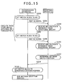
- step S100 when the high-frequency transmission system 100I is set to the calibration mode, the reception apparatus 300 transmits an IQ signal for testing from an antenna member of an output point 258 to the transmission apparatus 200 via a waveguide 220.
- step S214 upon determination of an optimum one of the antenna members 219a through 219d, the reception apparatus 300 feeds back a switching signal based on one of the antenna members 219a through 219d determined by the position rotational amount calculation block 270 to the transmission apparatus 200.
- the transmission apparatus 200 receives the switching signal via the antenna member 218a of the input point 218 and any one of the antenna members 219a through 219d of the input point 219.
- step S216 on the basis of the switching signal supplied from the reception apparatus 300, the transmission apparatus 200 switches to an optimum one of the antenna members 219a through 219d that makes the phase difference between modulation signals Sa and Sb be 90 degrees.
- the above-mentioned sequence of calibration operations allows the precision adjustment of the phase difference between modulation signals Sa and Sb, thereby realizing the high-speed transmission by use of IQ quadrature axis.
Landscapes
- Engineering & Computer Science (AREA)
- Computer Networks & Wireless Communication (AREA)
- Signal Processing (AREA)
- Transmitters (AREA)
- Digital Transmission Methods That Use Modulated Carrier Waves (AREA)
Applications Claiming Priority (1)
| Application Number | Priority Date | Filing Date | Title |
|---|---|---|---|
| JP2009093444A JP2010245905A (ja) | 2009-04-07 | 2009-04-07 | 送信装置および通信システム |
Publications (2)
| Publication Number | Publication Date |
|---|---|
| EP2239812A1 EP2239812A1 (en) | 2010-10-13 |
| EP2239812B1 true EP2239812B1 (en) | 2011-09-07 |
Family
ID=42340877
Family Applications (1)
| Application Number | Title | Priority Date | Filing Date |
|---|---|---|---|
| EP10002629A Not-in-force EP2239812B1 (en) | 2009-04-07 | 2010-03-12 | Transmission apparatus and communication system |
Country Status (6)
| Country | Link |
|---|---|
| US (1) | US8213534B2 (ja) |
| EP (1) | EP2239812B1 (ja) |
| JP (1) | JP2010245905A (ja) |
| CN (1) | CN101860506A (ja) |
| AT (1) | ATE523919T1 (ja) |
| BR (1) | BRPI1000681A2 (ja) |
Families Citing this family (6)
| Publication number | Priority date | Publication date | Assignee | Title |
|---|---|---|---|---|
| SG188012A1 (en) * | 2011-08-26 | 2013-03-28 | Sony Corp | An on pcb dielectric waveguide |
| CN103645380A (zh) * | 2013-12-04 | 2014-03-19 | 北京无线电计量测试研究所 | 一种用于毫米波的波导型的相位标准器的设计方法 |
| JP6162608B2 (ja) * | 2014-01-07 | 2017-07-12 | 日本電信電話株式会社 | 伝送システム |
| US10338873B2 (en) * | 2015-02-27 | 2019-07-02 | Hewlett-Packard Development Company, L.P. | Waveguides in a computing device |
| DE102019133684A1 (de) * | 2019-12-10 | 2021-06-10 | Sennheiser Electronic Gmbh & Co. Kg | Vorrichtung zur Konfiguration einer Drahtlos-Funkverbindung und Verfahren zur Konfiguration einer Drahtlos-Funkverbindung |
| CN110879387B (zh) * | 2019-12-17 | 2021-10-15 | 成都华创电科信息技术有限公司 | 一种基于无线电宽带信号测距仪 |
Family Cites Families (16)
| Publication number | Priority date | Publication date | Assignee | Title |
|---|---|---|---|---|
| GB1507147A (en) * | 1974-09-25 | 1978-04-12 | Marconi Co Ltd | Multiplexing arrangements |
| FR2610462A1 (fr) * | 1986-12-30 | 1988-08-05 | Thomson Csf | Dispositif et procede de modulation amplitude-phase utilisant une pluralite d'emetteurs |
| IT1277256B1 (it) * | 1995-10-13 | 1997-11-05 | Pirelli Cavi S P A Ora Pirelli | Commutatore acusto-ottico in guida d'onda, sintonizzabile, con cammini ottici equilibrati |
| JP2885713B2 (ja) | 1996-08-27 | 1999-04-26 | 埼玉日本電気株式会社 | 送信機 |
| JP2000209162A (ja) * | 1999-01-12 | 2000-07-28 | Hitachi Cable Ltd | 光波長多重用光源 |
| WO2001038925A1 (en) * | 1999-11-23 | 2001-05-31 | Nanovation Technologies, Inc. | Waveguide optical phase shifter |
| WO2002031965A1 (fr) * | 2000-10-12 | 2002-04-18 | Sony Corporation | Demodulateur et recepteur |
| GB2370473B (en) * | 2000-12-21 | 2004-04-07 | Marconi Caswell Ltd | Improvements in or relating to optical communication |
| JP2003209266A (ja) | 2001-08-31 | 2003-07-25 | Kanagawa Acad Of Sci & Technol | 誘電率変化方法、その方法を利用した光可変容量コンデンサ、紫外線センサ及び磁気センサ |
| US6657510B2 (en) * | 2001-11-27 | 2003-12-02 | Harris Corporation | Corrective phase quadrature modulator system and method |
| US7583897B2 (en) * | 2002-01-08 | 2009-09-01 | Enablence Usa Fttx Networks Inc. | Optical network system and method for supporting upstream signals propagated according to a cable modem protocol |
| GB0305619D0 (en) * | 2003-03-12 | 2003-04-16 | Qinetiq Ltd | Phase shifter device |
| KR100703410B1 (ko) * | 2005-01-19 | 2007-04-03 | 삼성전자주식회사 | 오프셋 직교위상편이 변조 방법과 이를 이용한 광송신기 |
| JP4760333B2 (ja) | 2005-11-28 | 2011-08-31 | セイコーエプソン株式会社 | 無線通信装置および無線通信方法 |
| CN100464191C (zh) * | 2007-05-18 | 2009-02-25 | 东南大学 | 微电子机械微波频率检测器及其制备方法 |
| JP4986800B2 (ja) | 2007-10-10 | 2012-07-25 | 双葉電子工業株式会社 | ロボット、ロボット用伝送路に使用される基準電圧生成回路ならびに基準電圧生成回路を有するハブ装置。 |
-
2009
- 2009-04-07 JP JP2009093444A patent/JP2010245905A/ja not_active Ceased
-
2010
- 2010-03-12 EP EP10002629A patent/EP2239812B1/en not_active Not-in-force
- 2010-03-12 AT AT10002629T patent/ATE523919T1/de not_active IP Right Cessation
- 2010-03-25 US US12/731,425 patent/US8213534B2/en not_active Expired - Fee Related
- 2010-03-31 BR BRPI1000681-8A patent/BRPI1000681A2/pt not_active IP Right Cessation
- 2010-03-31 CN CN201010151434A patent/CN101860506A/zh active Pending
Also Published As
| Publication number | Publication date |
|---|---|
| ATE523919T1 (de) | 2011-09-15 |
| EP2239812A1 (en) | 2010-10-13 |
| US20100254477A1 (en) | 2010-10-07 |
| CN101860506A (zh) | 2010-10-13 |
| BRPI1000681A2 (pt) | 2011-03-22 |
| US8213534B2 (en) | 2012-07-03 |
| JP2010245905A (ja) | 2010-10-28 |
Similar Documents
| Publication | Publication Date | Title |
|---|---|---|
| EP2239812B1 (en) | Transmission apparatus and communication system | |
| Tatu et al. | A new direct millimeter-wave six-port receiver | |
| De Wit et al. | Analysis and design of a foam-cladded PMF link with phase tuning in 28-nm CMOS | |
| US7859459B2 (en) | Phased array receivers and methods employing phase shifting downconverters | |
| Tatu et al. | Ka-band analog front-end for software-defined direct conversion receiver | |
| Ashtiani et al. | Direct multilevel carrier modulation using millimeter-wave balanced vector modulators | |
| US8750441B2 (en) | Signal cancellation to reduce phase noise, period jitter, and other contamination in local oscillator, frequency timing, or other timing generators or signal sources | |
| Zhang et al. | A high-precision hybrid analog and digital beamforming transceiver system for 5G millimeter-wave communication | |
| Kishimoto et al. | A 60-GHz band CMOS phased array transmitter utilizing compact baseband phase shifters | |
| KR20150008817A (ko) | 무선 주파수 시스템을 위한 시스템 및 방법 | |
| US11545950B2 (en) | Apparatus and methods for vector modulator phase shifters | |
| KR102405672B1 (ko) | Dgs를 포함하는 위상 천이기 및 이를 포함하는 전파 통신 모듈 | |
| US6853691B1 (en) | Vector modulator using amplitude invariant phase shifter | |
| Karakuzulu et al. | A Four-Channel Bidirectional $ D $-Band Phased-Array Transceiver for 200 Gb/s 6G Wireless Communications in a 130-nm BiCMOS Technology | |
| Standaert et al. | A 410 GHz OOK transmitter in 28 nm CMOS for short distance chip-to-chip communications | |
| Hagiwara et al. | A 258-GHz CMOS transmitter with phase-shifting architecture for phased-array systems | |
| Rieß et al. | An integrated 16-element phased-array transmitter front-end for wireless communication at 185 GHz | |
| McPherson et al. | 110 GHz vector modulator for adaptive software-controlled transmitters | |
| Oshima et al. | A X-band reconfigurable phased array antenna system using 0.13-µm SiGe BiCMOS IC with 5-bit IF phase shifters | |
| US11527831B2 (en) | Transmission and/or reception of radio signals | |
| Gueorguiev et al. | A 5.2 GHz CMOS I/Q modulator with integrated phase shifter for beamforming | |
| Venere et al. | Design of a multiport microwave modulator for dynamic polarization reconfiguration | |
| Yin et al. | A 1 Gbps 3.5-4.75 km communication link based on a 5G 28 GHz 8× 8 phased-array | |
| US11569579B2 (en) | Wireless data transmission using polarised electromagnetic radiation | |
| Lucyszyn et al. | Multi-level digital modulation performed directly at carrier frequency |
Legal Events
| Date | Code | Title | Description |
|---|---|---|---|
| PUAI | Public reference made under article 153(3) epc to a published international application that has entered the european phase |
Free format text: ORIGINAL CODE: 0009012 |
|
| 17P | Request for examination filed |
Effective date: 20100312 |
|
| AK | Designated contracting states |
Kind code of ref document: A1 Designated state(s): AT BE BG CH CY CZ DE DK EE ES FI FR GB GR HR HU IE IS IT LI LT LU LV MC MK MT NL NO PL PT RO SE SI SK SM TR |
|
| AX | Request for extension of the european patent |
Extension state: AL BA ME RS |
|
| GRAP | Despatch of communication of intention to grant a patent |
Free format text: ORIGINAL CODE: EPIDOSNIGR1 |
|
| RIC1 | Information provided on ipc code assigned before grant |
Ipc: H04L 27/36 20060101ALI20110203BHEP Ipc: H01P 1/18 20060101AFI20110203BHEP |
|
| GRAS | Grant fee paid |
Free format text: ORIGINAL CODE: EPIDOSNIGR3 |
|
| GRAA | (expected) grant |
Free format text: ORIGINAL CODE: 0009210 |
|
| REG | Reference to a national code |
Ref country code: GB Ref legal event code: FG4D |
|
| REG | Reference to a national code |
Ref country code: CH Ref legal event code: EP |
|
| REG | Reference to a national code |
Ref country code: IE Ref legal event code: FG4D |
|
| REG | Reference to a national code |
Ref country code: DE Ref legal event code: R096 Ref document number: 602010000163 Country of ref document: DE Effective date: 20111103 |
|
| REG | Reference to a national code |
Ref country code: NL Ref legal event code: VDEP Effective date: 20110907 |
|
| PG25 | Lapsed in a contracting state [announced via postgrant information from national office to epo] |
Ref country code: FI Free format text: LAPSE BECAUSE OF FAILURE TO SUBMIT A TRANSLATION OF THE DESCRIPTION OR TO PAY THE FEE WITHIN THE PRESCRIBED TIME-LIMIT Effective date: 20110907 Ref country code: SE Free format text: LAPSE BECAUSE OF FAILURE TO SUBMIT A TRANSLATION OF THE DESCRIPTION OR TO PAY THE FEE WITHIN THE PRESCRIBED TIME-LIMIT Effective date: 20110907 Ref country code: LT Free format text: LAPSE BECAUSE OF FAILURE TO SUBMIT A TRANSLATION OF THE DESCRIPTION OR TO PAY THE FEE WITHIN THE PRESCRIBED TIME-LIMIT Effective date: 20110907 Ref country code: HR Free format text: LAPSE BECAUSE OF FAILURE TO SUBMIT A TRANSLATION OF THE DESCRIPTION OR TO PAY THE FEE WITHIN THE PRESCRIBED TIME-LIMIT Effective date: 20110907 Ref country code: NO Free format text: LAPSE BECAUSE OF FAILURE TO SUBMIT A TRANSLATION OF THE DESCRIPTION OR TO PAY THE FEE WITHIN THE PRESCRIBED TIME-LIMIT Effective date: 20111207 |
|
| LTIE | Lt: invalidation of european patent or patent extension |
Effective date: 20110907 |
|
| PG25 | Lapsed in a contracting state [announced via postgrant information from national office to epo] |
Ref country code: SI Free format text: LAPSE BECAUSE OF FAILURE TO SUBMIT A TRANSLATION OF THE DESCRIPTION OR TO PAY THE FEE WITHIN THE PRESCRIBED TIME-LIMIT Effective date: 20110907 Ref country code: GR Free format text: LAPSE BECAUSE OF FAILURE TO SUBMIT A TRANSLATION OF THE DESCRIPTION OR TO PAY THE FEE WITHIN THE PRESCRIBED TIME-LIMIT Effective date: 20111208 Ref country code: LV Free format text: LAPSE BECAUSE OF FAILURE TO SUBMIT A TRANSLATION OF THE DESCRIPTION OR TO PAY THE FEE WITHIN THE PRESCRIBED TIME-LIMIT Effective date: 20110907 Ref country code: CY Free format text: LAPSE BECAUSE OF FAILURE TO SUBMIT A TRANSLATION OF THE DESCRIPTION OR TO PAY THE FEE WITHIN THE PRESCRIBED TIME-LIMIT Effective date: 20110907 Ref country code: AT Free format text: LAPSE BECAUSE OF FAILURE TO SUBMIT A TRANSLATION OF THE DESCRIPTION OR TO PAY THE FEE WITHIN THE PRESCRIBED TIME-LIMIT Effective date: 20110907 |
|
| REG | Reference to a national code |
Ref country code: AT Ref legal event code: MK05 Ref document number: 523919 Country of ref document: AT Kind code of ref document: T Effective date: 20110907 |
|
| PG25 | Lapsed in a contracting state [announced via postgrant information from national office to epo] |
Ref country code: BE Free format text: LAPSE BECAUSE OF FAILURE TO SUBMIT A TRANSLATION OF THE DESCRIPTION OR TO PAY THE FEE WITHIN THE PRESCRIBED TIME-LIMIT Effective date: 20110907 |
|
| PG25 | Lapsed in a contracting state [announced via postgrant information from national office to epo] |
Ref country code: CZ Free format text: LAPSE BECAUSE OF FAILURE TO SUBMIT A TRANSLATION OF THE DESCRIPTION OR TO PAY THE FEE WITHIN THE PRESCRIBED TIME-LIMIT Effective date: 20110907 Ref country code: SK Free format text: LAPSE BECAUSE OF FAILURE TO SUBMIT A TRANSLATION OF THE DESCRIPTION OR TO PAY THE FEE WITHIN THE PRESCRIBED TIME-LIMIT Effective date: 20110907 Ref country code: IS Free format text: LAPSE BECAUSE OF FAILURE TO SUBMIT A TRANSLATION OF THE DESCRIPTION OR TO PAY THE FEE WITHIN THE PRESCRIBED TIME-LIMIT Effective date: 20120107 |
|
| PGFP | Annual fee paid to national office [announced via postgrant information from national office to epo] |
Ref country code: FR Payment date: 20120403 Year of fee payment: 3 |
|
| PG25 | Lapsed in a contracting state [announced via postgrant information from national office to epo] |
Ref country code: RO Free format text: LAPSE BECAUSE OF FAILURE TO SUBMIT A TRANSLATION OF THE DESCRIPTION OR TO PAY THE FEE WITHIN THE PRESCRIBED TIME-LIMIT Effective date: 20110907 Ref country code: NL Free format text: LAPSE BECAUSE OF FAILURE TO SUBMIT A TRANSLATION OF THE DESCRIPTION OR TO PAY THE FEE WITHIN THE PRESCRIBED TIME-LIMIT Effective date: 20110907 Ref country code: PT Free format text: LAPSE BECAUSE OF FAILURE TO SUBMIT A TRANSLATION OF THE DESCRIPTION OR TO PAY THE FEE WITHIN THE PRESCRIBED TIME-LIMIT Effective date: 20120109 Ref country code: EE Free format text: LAPSE BECAUSE OF FAILURE TO SUBMIT A TRANSLATION OF THE DESCRIPTION OR TO PAY THE FEE WITHIN THE PRESCRIBED TIME-LIMIT Effective date: 20110907 Ref country code: PL Free format text: LAPSE BECAUSE OF FAILURE TO SUBMIT A TRANSLATION OF THE DESCRIPTION OR TO PAY THE FEE WITHIN THE PRESCRIBED TIME-LIMIT Effective date: 20110907 Ref country code: IT Free format text: LAPSE BECAUSE OF FAILURE TO SUBMIT A TRANSLATION OF THE DESCRIPTION OR TO PAY THE FEE WITHIN THE PRESCRIBED TIME-LIMIT Effective date: 20110907 |
|
| PGFP | Annual fee paid to national office [announced via postgrant information from national office to epo] |
Ref country code: DE Payment date: 20120323 Year of fee payment: 3 |
|
| PLBE | No opposition filed within time limit |
Free format text: ORIGINAL CODE: 0009261 |
|
| STAA | Information on the status of an ep patent application or granted ep patent |
Free format text: STATUS: NO OPPOSITION FILED WITHIN TIME LIMIT |
|
| PG25 | Lapsed in a contracting state [announced via postgrant information from national office to epo] |
Ref country code: DK Free format text: LAPSE BECAUSE OF FAILURE TO SUBMIT A TRANSLATION OF THE DESCRIPTION OR TO PAY THE FEE WITHIN THE PRESCRIBED TIME-LIMIT Effective date: 20110907 |
|
| 26N | No opposition filed |
Effective date: 20120611 |
|
| REG | Reference to a national code |
Ref country code: DE Ref legal event code: R097 Ref document number: 602010000163 Country of ref document: DE Effective date: 20120611 |
|
| PG25 | Lapsed in a contracting state [announced via postgrant information from national office to epo] |
Ref country code: MC Free format text: LAPSE BECAUSE OF NON-PAYMENT OF DUE FEES Effective date: 20120331 |
|
| REG | Reference to a national code |
Ref country code: IE Ref legal event code: MM4A |
|
| PG25 | Lapsed in a contracting state [announced via postgrant information from national office to epo] |
Ref country code: IE Free format text: LAPSE BECAUSE OF NON-PAYMENT OF DUE FEES Effective date: 20120312 |
|
| PG25 | Lapsed in a contracting state [announced via postgrant information from national office to epo] |
Ref country code: MK Free format text: LAPSE BECAUSE OF FAILURE TO SUBMIT A TRANSLATION OF THE DESCRIPTION OR TO PAY THE FEE WITHIN THE PRESCRIBED TIME-LIMIT Effective date: 20110907 |
|
| PG25 | Lapsed in a contracting state [announced via postgrant information from national office to epo] |
Ref country code: ES Free format text: LAPSE BECAUSE OF FAILURE TO SUBMIT A TRANSLATION OF THE DESCRIPTION OR TO PAY THE FEE WITHIN THE PRESCRIBED TIME-LIMIT Effective date: 20111218 |
|
| PG25 | Lapsed in a contracting state [announced via postgrant information from national office to epo] |
Ref country code: BG Free format text: LAPSE BECAUSE OF FAILURE TO SUBMIT A TRANSLATION OF THE DESCRIPTION OR TO PAY THE FEE WITHIN THE PRESCRIBED TIME-LIMIT Effective date: 20111207 |
|
| PG25 | Lapsed in a contracting state [announced via postgrant information from national office to epo] |
Ref country code: MT Free format text: LAPSE BECAUSE OF FAILURE TO SUBMIT A TRANSLATION OF THE DESCRIPTION OR TO PAY THE FEE WITHIN THE PRESCRIBED TIME-LIMIT Effective date: 20110907 |
|
| REG | Reference to a national code |
Ref country code: FR Ref legal event code: ST Effective date: 20131129 |
|
| REG | Reference to a national code |
Ref country code: DE Ref legal event code: R119 Ref document number: 602010000163 Country of ref document: DE Effective date: 20131001 |
|
| PG25 | Lapsed in a contracting state [announced via postgrant information from national office to epo] |
Ref country code: FR Free format text: LAPSE BECAUSE OF NON-PAYMENT OF DUE FEES Effective date: 20130402 Ref country code: DE Free format text: LAPSE BECAUSE OF NON-PAYMENT OF DUE FEES Effective date: 20131001 |
|
| PG25 | Lapsed in a contracting state [announced via postgrant information from national office to epo] |
Ref country code: TR Free format text: LAPSE BECAUSE OF FAILURE TO SUBMIT A TRANSLATION OF THE DESCRIPTION OR TO PAY THE FEE WITHIN THE PRESCRIBED TIME-LIMIT Effective date: 20110907 |
|
| PG25 | Lapsed in a contracting state [announced via postgrant information from national office to epo] |
Ref country code: LU Free format text: LAPSE BECAUSE OF NON-PAYMENT OF DUE FEES Effective date: 20120312 Ref country code: SM Free format text: LAPSE BECAUSE OF FAILURE TO SUBMIT A TRANSLATION OF THE DESCRIPTION OR TO PAY THE FEE WITHIN THE PRESCRIBED TIME-LIMIT Effective date: 20110907 |
|
| PG25 | Lapsed in a contracting state [announced via postgrant information from national office to epo] |
Ref country code: HU Free format text: LAPSE BECAUSE OF FAILURE TO SUBMIT A TRANSLATION OF THE DESCRIPTION OR TO PAY THE FEE WITHIN THE PRESCRIBED TIME-LIMIT Effective date: 20100312 |
|
| REG | Reference to a national code |
Ref country code: CH Ref legal event code: PL |
|
| GBPC | Gb: european patent ceased through non-payment of renewal fee |
Effective date: 20140312 |
|
| PG25 | Lapsed in a contracting state [announced via postgrant information from national office to epo] |
Ref country code: GB Free format text: LAPSE BECAUSE OF NON-PAYMENT OF DUE FEES Effective date: 20140312 Ref country code: LI Free format text: LAPSE BECAUSE OF NON-PAYMENT OF DUE FEES Effective date: 20140331 Ref country code: CH Free format text: LAPSE BECAUSE OF NON-PAYMENT OF DUE FEES Effective date: 20140331 |