EP2237335B1 - Method for fabricating a white-light emitting light emitting diode chip - Google Patents
Method for fabricating a white-light emitting light emitting diode chip Download PDFInfo
- Publication number
- EP2237335B1 EP2237335B1 EP09010450.6A EP09010450A EP2237335B1 EP 2237335 B1 EP2237335 B1 EP 2237335B1 EP 09010450 A EP09010450 A EP 09010450A EP 2237335 B1 EP2237335 B1 EP 2237335B1
- Authority
- EP
- European Patent Office
- Prior art keywords
- blue
- light led
- led chip
- light
- white
- Prior art date
- Legal status (The legal status is an assumption and is not a legal conclusion. Google has not performed a legal analysis and makes no representation as to the accuracy of the status listed.)
- Not-in-force
Links
- 238000000034 method Methods 0.000 title claims description 44
- OAICVXFJPJFONN-UHFFFAOYSA-N Phosphorus Chemical compound [P] OAICVXFJPJFONN-UHFFFAOYSA-N 0.000 claims description 44
- 239000010410 layer Substances 0.000 claims description 43
- 239000000758 substrate Substances 0.000 claims description 19
- 239000011241 protective layer Substances 0.000 claims description 16
- 239000000463 material Substances 0.000 claims description 14
- 238000000465 moulding Methods 0.000 claims description 4
- 229920002120 photoresistant polymer Polymers 0.000 description 14
- 238000000576 coating method Methods 0.000 description 9
- 239000011248 coating agent Substances 0.000 description 8
- 239000004065 semiconductor Substances 0.000 description 5
- 229910002601 GaN Inorganic materials 0.000 description 3
- 238000005229 chemical vapour deposition Methods 0.000 description 3
- 239000002245 particle Substances 0.000 description 3
- JMASRVWKEDWRBT-UHFFFAOYSA-N Gallium nitride Chemical compound [Ga]#N JMASRVWKEDWRBT-UHFFFAOYSA-N 0.000 description 2
- 238000010521 absorption reaction Methods 0.000 description 2
- 239000012790 adhesive layer Substances 0.000 description 2
- PNEYBMLMFCGWSK-UHFFFAOYSA-N aluminium oxide Inorganic materials [O-2].[O-2].[O-2].[Al+3].[Al+3] PNEYBMLMFCGWSK-UHFFFAOYSA-N 0.000 description 2
- 229910052593 corundum Inorganic materials 0.000 description 2
- 229910052751 metal Inorganic materials 0.000 description 2
- 239000002184 metal Substances 0.000 description 2
- 238000004806 packaging method and process Methods 0.000 description 2
- SBIBMFFZSBJNJF-UHFFFAOYSA-N selenium;zinc Chemical compound [Se]=[Zn] SBIBMFFZSBJNJF-UHFFFAOYSA-N 0.000 description 2
- 239000010409 thin film Substances 0.000 description 2
- 235000012431 wafers Nutrition 0.000 description 2
- 229910001845 yogo sapphire Inorganic materials 0.000 description 2
- XUIMIQQOPSSXEZ-UHFFFAOYSA-N Silicon Chemical compound [Si] XUIMIQQOPSSXEZ-UHFFFAOYSA-N 0.000 description 1
- 150000001875 compounds Chemical class 0.000 description 1
- 230000008878 coupling Effects 0.000 description 1
- 238000010168 coupling process Methods 0.000 description 1
- 238000005859 coupling reaction Methods 0.000 description 1
- 230000001419 dependent effect Effects 0.000 description 1
- 238000010586 diagram Methods 0.000 description 1
- 238000007598 dipping method Methods 0.000 description 1
- 230000005684 electric field Effects 0.000 description 1
- 238000001652 electrophoretic deposition Methods 0.000 description 1
- 239000003822 epoxy resin Substances 0.000 description 1
- 239000011521 glass Substances 0.000 description 1
- 229910052738 indium Inorganic materials 0.000 description 1
- APFVFJFRJDLVQX-UHFFFAOYSA-N indium atom Chemical compound [In] APFVFJFRJDLVQX-UHFFFAOYSA-N 0.000 description 1
- 238000004519 manufacturing process Methods 0.000 description 1
- 230000000873 masking effect Effects 0.000 description 1
- 238000002161 passivation Methods 0.000 description 1
- 238000000206 photolithography Methods 0.000 description 1
- 229920000647 polyepoxide Polymers 0.000 description 1
- 238000004549 pulsed laser deposition Methods 0.000 description 1
- 238000007650 screen-printing Methods 0.000 description 1
- 229910052710 silicon Inorganic materials 0.000 description 1
- 239000010703 silicon Substances 0.000 description 1
- 230000003595 spectral effect Effects 0.000 description 1
- 238000001228 spectrum Methods 0.000 description 1
- 238000005507 spraying Methods 0.000 description 1
- 238000004544 sputter deposition Methods 0.000 description 1
- 238000001429 visible spectrum Methods 0.000 description 1
Images


Classifications
-
- H—ELECTRICITY
- H10—SEMICONDUCTOR DEVICES; ELECTRIC SOLID-STATE DEVICES NOT OTHERWISE PROVIDED FOR
- H10H—INORGANIC LIGHT-EMITTING SEMICONDUCTOR DEVICES HAVING POTENTIAL BARRIERS
- H10H20/00—Individual inorganic light-emitting semiconductor devices having potential barriers, e.g. light-emitting diodes [LED]
- H10H20/80—Constructional details
- H10H20/85—Packages
- H10H20/851—Wavelength conversion means
- H10H20/8516—Wavelength conversion means having a non-uniform spatial arrangement or non-uniform concentration, e.g. patterned wavelength conversion layer or wavelength conversion layer with a concentration gradient
Definitions
- the invention relates to a method for fabricating a light-emitting diode (LED) chip and more particularly to a method for fabricating a white-light LED chip.
- LED light-emitting diode
- Light-emitting diode is a compound semiconductor device that energy transfers electrical current into light.
- the light emitted by an LED is distributed across a spectrum that is approximately 20 ⁇ 40nm wide and has a peak emission wavelength defined by the semiconductor material of a light-emitting layer of the LED.
- a peak emission wavelength As a consequence of the peak emission wavelength, a single LED cannot emit white light, which is composed of spectral contributions from almost the entire wavelength range of the visible spectrum.
- Fig. 1 shows a cross section of a conventional white light emitting device 100.
- the white light emitting device 100 includes a blue-light LED chip 12 disposed in a reflective cup 10 and surrounded by phosphors 14.
- a glass plate 16 is disposed on the reflective cup 10, covering the LED chip 12 and the phosphors 14.
- a portion of the blue light emitted by the LED chip 12, and the red and the green light emitted by the phosphor 14 as a result of a partial absorption of the blue light can combined to produce white light.
- white light generated by sources such as the device illustrated in Fig. 1 is not uniform in color. This non-uniformity is a consequence of the variations in the thickness of the phosphors 14 surrounding the LED chip 12. The variations in the thickness cause spatially non-uniform absorption of blue light and emission of red and green light. Therefore, the generated white light is surrounded by colored rings.
- U.S. Pat. No. 6,576,488 discloses a method for conformally coating a light emitting semiconductor structure, such as an LED chip, with a phosphor layer.
- the method involves electrically coupling an LED chip to a submount, applying a first bias voltage to the submount, and applying a second bias voltage to a solution of charged (pumped) phosphor particles.
- the electric field created by the two bias voltages induces the phosphor particles to deposit on the conductive surface, such as the surfaces of the submount and the LED chip.
- using the electrophoretic deposition process to form a phosphor layer on a LED chip has some problems.
- the adhesion between the phosphor particles and the surface of the LED chip is weak, such that the phosphor layer is easily separated from the LED chip.
- U.S. Pat. No. 6,576,488 discloses using a chemical vapor deposition (CVD) process to form a tinted thin film of a yellow color material on a blue LED element.
- CVD chemical vapor deposition
- This method can improve light uniformity and the light output is not heavily dependent on the thickness of a substrate of an LED chip.
- the process of this method is complicated, as passivation layers that cover the LED chip need to be formed. Additionally, it is difficult to control the process for forming the tinted thin film of the yellow color material on the LED chip by the CVD process.
- US 2007/0159067 A1 discloses a method for fabricating a LED device generating light of multi-wavelengths.
- a blue-light LED-chip having electrode pads on its top surface is attached with its bottom surface on a substrate.
- a mask pattern preferably a photoresist or an insulating layer, is formed on the electrode pads.
- a phosphor layer is formed by a sputtering method or a pulsed laser deposition method on the surface of the LED chip except for the electrode pads masked by the mask pattern, whereafter the mask pattern is removed.
- US 2007/0228404 A1 is concerned with methods for producing white-light emitting diodes.
- a plurality of vertical blue light LED chips are provided on a substrate.
- a phosphor coating is formed on the entire surface of the LED chips by using a spin coater, screen printing, roller method or dipping method.
- a photoresist layer is applied to the phosphor coating and exposed with a contact pattern.
- the phosphor layer is then etched to form a patterned phosphor layer.
- a contact metal layer is deposited on top of the photoresist layer and the photoresist layer is removed to form bonding pads.
- the process for phosphor coating and forming the bonding pad can be exchanged, wherein the contact metal layer is patterned, dry edged and protected first by a photoresist masking layer before the phosphor layer is applied and patterned by lift-off techniques during the removal of the photoresist layer.
- US 2008/0173884 A1 teaches a method for fabricating LED chips comprising: providing a plurality of LEDs on a substrate, forming pedestals on the LEDs, each of the pedestals being in electrical contact with one of the LEDs, forming a coating over said LEDs, with the coating burying at least some of the pedestals, The coating being subsequently planarized leaving some of said coating material on said LEDs while exposing at least some of the buried pedestals, making them available for contacting.
- a white-light LED chip and a fabrication method thereof are provided.
- the white-light LED chip does not require a package for white light emission.
- An exemplary embodiment of the white-light LED chip comprises a blue-light LED chip having a top surface and a bottom surface.
- a phosphor layer is disposed on the top surface of the blue-light LED chip, wherein the phosphor layer is directly in contact with the top surface of the blue-light LED chip.
- An exemplary embodiment of the method for fabricating the white-light LED chip comprises providing a plurality of blue-light LED chips, having a top surface and a bottom surface, wherein each blue-light LED chip has at least one contact pad on the top surface of the blue-light LED chip.
- the bottom surfaces of the blue-light LED chips are attached on a substrate.
- a protective layer is formed on the contact pads, exposing the top surface of the blue-light LED chips.
- a phosphor material is formed on the top surface of the blue-light LED chips.
- a mold is provided on the phosphor material to form a phosphor layer on the top surface of the blue-light LED chips except for the area of the contact pad on the top surface of the blue-light LED chip.
- the protective layer is removed from the contact pads, and the substrate is divided between the adjacent blue-light LED chips to form a plurality of white-light LED chips.
- the white-light LED chip 200 comprises a blue-light LED chip 201 and a phosphor layer 207 disposed on a top surface of the blue-light LED chip 201.
- the blue-light LED chip 201 is a vertical LED chip which has an n-contact pad 203 disposed on the top surface of the LED chip 201 and a p-contact pad 205 disposed on a bottom surface of the LED chip 201.
- the top surface of the blue-light LED chip 201 is the light emitting surface and the bottom surface thereof is the opposite surface to the top surface.
- the top surface of the blue-light LED chip 201 is directly covered with the phosphor layer 207 except for the area of the n-contact pad 203.
- the white-light LED chip 300 comprises a blue-light LED chip 201 and a phosphor layer 207 disposed on a top surface of the blue-light LED chip 201.
- the blue-light LED chip 201 is a lateral LED chip which has an n-contact pad 203 and a p-contact pad 205 disposed on the top surface of the LED chip 201.
- the top surface of the blue-light LED chip 201 is directly covered with the phosphor layer 207 except for the area of the n-contact pad 203 and the p-contact pad 205.
- the blue-light LED chip 201 includes an n-type region, an active region and a p-type region, wherein the active region is disposed between the n-type region and the p-type region.
- the n-contact pad 203 is associated with the n-type region and the p-contact pad 205 is associated with the p-type region.
- the variety of regions in the blue-light LED chip 201 is not depicted.
- the active region can be comprised of Gallium-Nitride (GaN) and Indium to produce InGaN/GaN semiconductor layers.
- the n-type region can be an n-GaN layer and a p-type region can be a p-GaN layer. Electrical power is applied to the n-contact pad 203 and p-contact pad 205 which cause the LED chip 201 to emit blue light.
- the phosphor layer 207 contains luminescent materials which can convert a portion of the blue light emitted by the LED chip 201 into yellow light.
- the luminescent materials of the phosphor layer 207 may be ZnSe, CeO, Al 2 O 3 , and Y 2 O 3 : Ce.
- the yellow light of the phosphor layer 207 is combined with the blue light emitted by the LED chip 201 to form a white light.
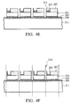
- Figs. 4A to 4F are cross sections of an exemplary embodiment of a method for fabricating the white-light LED chip of Fig.2 according to the invention.
- a plurality of blue-light LED chips 201 are provided to be disposed adjacent to each other on a temporary substrate 211.
- the temporary substrate 211 may be a silicon wafer or other semiconductor wafers, which is removed after the white-light LED chip is completed.
- an adhesive layer 209 such as epoxy resin is formed on the substrate 211.
- the bottom surface of the blue-light LED chip 201 is attached to the substrate 211 through the adhesive layer 209.
- the p-contact pad 205 of the blue-light LED chips 201 is attached to the substrate 211.
- a protective layer 213 is formed on the n-contact pads 203 of the blue-light LED chips 20, exposing the other top surfaces of the blue-light LED chips 201.
- the protective layer 213 may be a photoresist which is patterned by a photolithography process to form the protective layer 213 on the n-contact pads 203.
- the protective layer 213 can also be a hard mask which has a pattern corresponding to the n-contact pads 203.
- a photoresist or a hard mask 212 is disposed on the temporary substrate 211 and between the blue-light LED chips 201.
- the materials of the photoresist or the hard mask 212 may be the same as the protective layer 213, and the photoresist or the hard mask 212 can be formed together with the protective layer 213.
- a phosphor material 207 is formed on the top surface of the blue-light LED chips 201 by a spray coating, a dispensing process or other coating processes.
- the phosphor material 207 is such as ZnSe, CeO, Al 2 O 3 , and Y 2 O 3 : Ce which can convert a portion of the blue light emitted by the LED chip 201 into a yellow light.
- a mold 217 is provided to mold the phosphor material 207 into a phosphor layer.
- the phosphor layer 207 is formed on the top surface of the blue-light LED chip 201 except for the area of the n-contact pad 203. Meanwhile, the n-contact pad 203 is protected by the protective layer 213.
- the mold 217 is removed after the phosphor layer 207 is formed.
- the photoresist or the hard mask 212 is also removed from the temporary substrate 211.
- the photoresist 212 can be removed by a development process.
- the hrad mask 212 can be removed by a stripping process.
- the photoresist or the hard mask 212 is removed, only the top surface of the blue-light LED chip 201 is covered with the phosphor layer 207 and the sidewalls of the blue-light LED chip 201 are not covered with the phosphor layer 207.
- the protective layer 213 is removed from the n-contact pad 203.
- the protective layer 213 may be a photoresist which can be removed by a development process.
- the protective layer 213 may be a hard mask which can be directly removed by a stripping process.
- the substrate 211 is divided along a scribe line 219 between the adjacent blue-light LED chips 201.
- the bottom surface of the blue-light LED chip 201 is separated from the temporary substrate 211 to form the white-light LED chip 200 as shown in Fig. 2 .
- the method for fabricating the white-light LED chip 300 of Fig.3 according to the invention is the same as the embodiment of Figs. 4A to 4F , except that the n-contact pad 203 and the p-contact pad 205 are both disposed on the top surface of the blue-light LED chip 201. Meanwhile, in the process for fabricating the white-light LED chip 300, the n-contact pad 203 and the p-contact pad 205 are both covered with the protective layer 213. In addition, a mold used for the white-light LED chip 300 is different from the mold 217 used in the white-light LED chip 200. As a result of a molding process for the white-light LED chip 300, the phosphor layer 207 is formed on the top surface of the blue-light LED chip 201 to expose the n-contact pad 203 and the p-contact pad 205.
- the n-contact pad 203 is disposed on the top surface of the blue-light LED chip 201 and the p-contact pad 205 is disposed on the bottom surface of the blue-light LED chip 201.
- the vertical white-light LED chip can also have an n-contact pad on the bottom surface of the LED chip and a p-contact pad on the top surface of the LED chip.
- the white-light LED chips 200 and 300 can be used to emit white light without packaging.
- the white-light LED chips 200 and 300 can also be a part of another assembly such as displays or illuminative devices which provide white light emissions.
- the white-light LED chips of the invention can provide white light emissions without packaging the blue-light LED chips.
- the phosphor layer is directly disposed on the top surface of the blue-light LED chip and can convert a portion of blue light emitted by the blue-light LED chip into yellow light. Therefore, the yellow light from the phosphor layer is combined with the blue light from the blue-light LED chip to form a white light. Accordingly, the white-light LED chips of the invention do not need packages.
- the white-light LED chips according to the embodiments of the invention can produce uniform white light due to uniform thickness of the phosphor layer on the blue-light LED chip.
Landscapes
- Led Device Packages (AREA)
- Led Devices (AREA)
Description
- The invention relates to a method for fabricating a light-emitting diode (LED) chip and more particularly to a method for fabricating a white-light LED chip.
- Light-emitting diode (LED) is a compound semiconductor device that energy transfers electrical current into light. The light emitted by an LED is distributed across a spectrum that is approximately 20~40nm wide and has a peak emission wavelength defined by the semiconductor material of a light-emitting layer of the LED. As a consequence of the peak emission wavelength, a single LED cannot emit white light, which is composed of spectral contributions from almost the entire wavelength range of the visible spectrum.
Fig. 1 shows a cross section of a conventional whitelight emitting device 100. The whitelight emitting device 100 includes a blue-light LED chip 12 disposed in areflective cup 10 and surrounded byphosphors 14. Aglass plate 16 is disposed on thereflective cup 10, covering theLED chip 12 and thephosphors 14. In the exemplary device ofFig. 1 , a portion of the blue light emitted by theLED chip 12, and the red and the green light emitted by thephosphor 14 as a result of a partial absorption of the blue light can combined to produce white light. - However, white light generated by sources such as the device illustrated in
Fig. 1 is not uniform in color. This non-uniformity is a consequence of the variations in the thickness of thephosphors 14 surrounding theLED chip 12. The variations in the thickness cause spatially non-uniform absorption of blue light and emission of red and green light. Therefore, the generated white light is surrounded by colored rings. -
U.S. Pat. No. 6,576,488 discloses a method for conformally coating a light emitting semiconductor structure, such as an LED chip, with a phosphor layer. The method involves electrically coupling an LED chip to a submount, applying a first bias voltage to the submount, and applying a second bias voltage to a solution of charged (pumped) phosphor particles. The electric field created by the two bias voltages induces the phosphor particles to deposit on the conductive surface, such as the surfaces of the submount and the LED chip. However, using the electrophoretic deposition process to form a phosphor layer on a LED chip has some problems. The adhesion between the phosphor particles and the surface of the LED chip is weak, such that the phosphor layer is easily separated from the LED chip.U.S. Pat. No. 6,576,488 discloses using a chemical vapor deposition (CVD) process to form a tinted thin film of a yellow color material on a blue LED element. This method can improve light uniformity and the light output is not heavily dependent on the thickness of a substrate of an LED chip. However, the process of this method is complicated, as passivation layers that cover the LED chip need to be formed. Additionally, it is difficult to control the process for forming the tinted thin film of the yellow color material on the LED chip by the CVD process. - Therefore, a white-light LED chip with uniformity in color that is capable of overcoming the above problems is desired.
-
US 2007/0159067 A1 discloses a method for fabricating a LED device generating light of multi-wavelengths. Herein, a blue-light LED-chip having electrode pads on its top surface is attached with its bottom surface on a substrate. Thereafter, a mask pattern, preferably a photoresist or an insulating layer, is formed on the electrode pads. A phosphor layer is formed by a sputtering method or a pulsed laser deposition method on the surface of the LED chip except for the electrode pads masked by the mask pattern, whereafter the mask pattern is removed. -
US 2007/0228404 A1 is concerned with methods for producing white-light emitting diodes. Herein, a plurality of vertical blue light LED chips are provided on a substrate. A phosphor coating is formed on the entire surface of the LED chips by using a spin coater, screen printing, roller method or dipping method. A photoresist layer is applied to the phosphor coating and exposed with a contact pattern. The phosphor layer is then etched to form a patterned phosphor layer. Thereafter, a contact metal layer is deposited on top of the photoresist layer and the photoresist layer is removed to form bonding pads. Alternatively, the process for phosphor coating and forming the bonding pad can be exchanged, wherein the contact metal layer is patterned, dry edged and protected first by a photoresist masking layer before the phosphor layer is applied and patterned by lift-off techniques during the removal of the photoresist layer. -
US 2008/0173884 A1 teaches a method for fabricating LED chips comprising: providing a plurality of LEDs on a substrate, forming pedestals on the LEDs, each of the pedestals being in electrical contact with one of the LEDs, forming a coating over said LEDs, with the coating burying at least some of the pedestals, The coating being subsequently planarized leaving some of said coating material on said LEDs while exposing at least some of the buried pedestals, making them available for contacting. - It is an object of the present invention to provide a method for fabricating a white-light LED chip that can produce uniform white light.
- This object is solved by the method for fabricating a white-light LED chip according to claim 1.
- A white-light LED chip and a fabrication method thereof are provided. The white-light LED chip does not require a package for white light emission. An exemplary embodiment of the white-light LED chip comprises a blue-light LED chip having a top surface and a bottom surface. A phosphor layer is disposed on the top surface of the blue-light LED chip, wherein the phosphor layer is directly in contact with the top surface of the blue-light LED chip.
- An exemplary embodiment of the method for fabricating the white-light LED chip comprises providing a plurality of blue-light LED chips, having a top surface and a bottom surface, wherein each blue-light LED chip has at least one contact pad on the top surface of the blue-light LED chip. The bottom surfaces of the blue-light LED chips are attached on a substrate. A protective layer is formed on the contact pads, exposing the top surface of the blue-light LED chips. A phosphor material is formed on the top surface of the blue-light LED chips. A mold is provided on the phosphor material to form a phosphor layer on the top surface of the blue-light LED chips except for the area of the contact pad on the top surface of the blue-light LED chip. Then, the protective layer is removed from the contact pads, and the substrate is divided between the adjacent blue-light LED chips to form a plurality of white-light LED chips.
- A detailed description is given in the following embodiments with reference to the accompanying drawings.
- The invention can be more fully understood by reading the subsequent detailed description and examples with references made to the accompanying drawings, wherein:
-
Fig. 1 is a schematic cross section of a conventional white light emitting device; -
Fig. 2 is a schematic cross section of a white-light LED chip according to one embodiment of the invention; -
Fig. 3 is a schematic cross section of a white-light LED chip according to another embodiment of the invention; and -
Figs. 4A to 4F are cross sections of an exemplary embodiment of a method for fabricating the white-light LED chip ofFig. 2 according to the invention. - The following description is of the best-contemplated mode of carrying out the invention. This description is made for the purpose of illustrating the general principles of the invention and should not be taken in a limiting sense. The scope of the invention is determined by the appended claims.
- The invention provides white-light LED chips that do not require a package for white light emissions.
Figs. 2 and 3 show cross sections of exemplary embodiments of a white-light LED chip fabricated by the method according to the invention. Referring toFig. 2 , the white-light LED chip 200 comprises a blue-light LED chip 201 and aphosphor layer 207 disposed on a top surface of the blue-light LED chip 201. In this embodiment, the blue-light LED chip 201 is a vertical LED chip which has an n-contact pad 203 disposed on the top surface of theLED chip 201 and a p-contact pad 205 disposed on a bottom surface of theLED chip 201. The top surface of the blue-light LED chip 201 is the light emitting surface and the bottom surface thereof is the opposite surface to the top surface. The top surface of the blue-light LED chip 201 is directly covered with thephosphor layer 207 except for the area of the n-contact pad 203. - Referring to
Fig. 3 , another embodiment of a white-light LED chip 300 fabricated by the method according to the invention is shown. The white-light LED chip 300 comprises a blue-light LED chip 201 and aphosphor layer 207 disposed on a top surface of the blue-light LED chip 201. In this embodiment, the blue-light LED chip 201 is a lateral LED chip which has an n-contact pad 203 and a p-contact pad 205 disposed on the top surface of theLED chip 201. The top surface of the blue-light LED chip 201 is directly covered with thephosphor layer 207 except for the area of the n-contact pad 203 and the p-contact pad 205. - In general, the blue-
light LED chip 201 includes an n-type region, an active region and a p-type region, wherein the active region is disposed between the n-type region and the p-type region. The n-contact pad 203 is associated with the n-type region and the p-contact pad 205 is associated with the p-type region. In order to simplify the diagram, the variety of regions in the blue-light LED chip 201 is not depicted. In some embodiments, the active region can be comprised of Gallium-Nitride (GaN) and Indium to produce InGaN/GaN semiconductor layers. The n-type region can be an n-GaN layer and a p-type region can be a p-GaN layer. Electrical power is applied to the n-contact pad 203 and p-contact pad 205 which cause theLED chip 201 to emit blue light. Thephosphor layer 207 contains luminescent materials which can convert a portion of the blue light emitted by theLED chip 201 into yellow light. The luminescent materials of thephosphor layer 207 may be ZnSe, CeO, Al2O3, and Y2O3: Ce. Thus, the yellow light of thephosphor layer 207 is combined with the blue light emitted by theLED chip 201 to form a white light. - Referring to
Figs. 4A to 4F , which are cross sections of an exemplary embodiment of a method for fabricating the white-light LED chip ofFig.2 according to the invention. As shown inFig. 4A , a plurality of blue-light LED chips 201 are provided to be disposed adjacent to each other on atemporary substrate 211. Thetemporary substrate 211 may be a silicon wafer or other semiconductor wafers, which is removed after the white-light LED chip is completed. In one embodiment, anadhesive layer 209 such as epoxy resin is formed on thesubstrate 211. The bottom surface of the blue-light LED chip 201 is attached to thesubstrate 211 through theadhesive layer 209. In this embodiment, the p-contact pad 205 of the blue-light LED chips 201 is attached to thesubstrate 211. - Referring to
Fig. 4B , aprotective layer 213 is formed on the n-contact pads 203 of the blue-light LED chips 20, exposing the other top surfaces of the blue-light LED chips 201. Theprotective layer 213 may be a photoresist which is patterned by a photolithography process to form theprotective layer 213 on the n-contact pads 203. Theprotective layer 213 can also be a hard mask which has a pattern corresponding to the n-contact pads 203. In addition, a photoresist or ahard mask 212 is disposed on thetemporary substrate 211 and between the blue-light LED chips 201. The materials of the photoresist or thehard mask 212 may be the same as theprotective layer 213, and the photoresist or thehard mask 212 can be formed together with theprotective layer 213. Then, referring toFig. 4C , aphosphor material 207 is formed on the top surface of the blue-light LED chips 201 by a spray coating, a dispensing process or other coating processes. Thephosphor material 207 is such as ZnSe, CeO, Al2O3, and Y2O3: Ce which can convert a portion of the blue light emitted by theLED chip 201 into a yellow light. - Referring to
Fig. 4D , amold 217 is provided to mold thephosphor material 207 into a phosphor layer. As a result of the molding process, thephosphor layer 207 is formed on the top surface of the blue-light LED chip 201 except for the area of the n-contact pad 203. Meanwhile, the n-contact pad 203 is protected by theprotective layer 213. Then, as shown inFig. 4E , themold 217 is removed after thephosphor layer 207 is formed. In addition, the photoresist or thehard mask 212 is also removed from thetemporary substrate 211. Thephotoresist 212 can be removed by a development process. Thehrad mask 212 can be removed by a stripping process. After the photoresist or thehard mask 212 is removed, only the top surface of the blue-light LED chip 201 is covered with thephosphor layer 207 and the sidewalls of the blue-light LED chip 201 are not covered with thephosphor layer 207. - Referring to
Fig. 4F , theprotective layer 213 is removed from the n-contact pad 203. In one embodiment, theprotective layer 213 may be a photoresist which can be removed by a development process. In another embodiment, theprotective layer 213 may be a hard mask which can be directly removed by a stripping process. After removing theprotective layer 213, thesubstrate 211 is divided along ascribe line 219 between the adjacent blue-light LED chips 201. Then, the bottom surface of the blue-light LED chip 201 is separated from thetemporary substrate 211 to form the white-light LED chip 200 as shown inFig. 2 . - In another embodiment, the method for fabricating the white-
light LED chip 300 ofFig.3 according to the invention is the same as the embodiment ofFigs. 4A to 4F , except that the n-contact pad 203 and the p-contact pad 205 are both disposed on the top surface of the blue-light LED chip 201. Meanwhile, in the process for fabricating the white-light LED chip 300, the n-contact pad 203 and the p-contact pad 205 are both covered with theprotective layer 213. In addition, a mold used for the white-light LED chip 300 is different from themold 217 used in the white-light LED chip 200. As a result of a molding process for the white-light LED chip 300, thephosphor layer 207 is formed on the top surface of the blue-light LED chip 201 to expose the n-contact pad 203 and the p-contact pad 205. - Although in the embodiment of the vertical white-
light LED chip 200, the n-contact pad 203 is disposed on the top surface of the blue-light LED chip 201 and the p-contact pad 205 is disposed on the bottom surface of the blue-light LED chip 201. In other embodiments of the invention, the vertical white-light LED chip can also have an n-contact pad on the bottom surface of the LED chip and a p-contact pad on the top surface of the LED chip. - The white-
light LED chips light LED chips - According to the aforementioned embodiments, the white-light LED chips of the invention can provide white light emissions without packaging the blue-light LED chips. The phosphor layer is directly disposed on the top surface of the blue-light LED chip and can convert a portion of blue light emitted by the blue-light LED chip into yellow light. Therefore, the yellow light from the phosphor layer is combined with the blue light from the blue-light LED chip to form a white light. Accordingly, the white-light LED chips of the invention do not need packages. Moreover, the white-light LED chips according to the embodiments of the invention can produce uniform white light due to uniform thickness of the phosphor layer on the blue-light LED chip.
Claims (5)
- A method for fabricating a white-light LED chip, comprising the ordered steps of:- providing a plurality of blue-light LED chips (201), having a top surface and a bottom surface, wherein each blue-light LED chip (201) has at least one contact pad (203) on the top surface of the blue-light LED chip (201);- attaching the bottom surfaces of the blue-light LED chips (201) on a substrate (211);- forming a protective layer (213) on the contact pads (203) of the top surfaces of the blue-light LED chips (201);- forming a phosphor material (207) on the top surfaces of the blue-light LED chips (201) including areas of the contact pads (203);- providing a mold (217) and performing a molding process on the phosphor material (207) to form a pattern of a phosphor layer (207) on the top surfaces of the blue-light LED chips (201) whereby as a result of the molding process, the phosphor layer is formed on the top surfaces of the blue-light LED chips except for areas of the contact pads (203);- removing the mold (217) after forming the pattern of the phosphor layer (207);- removing the protective layer (213) from the contact pads (203); and- dividing the substrate (211) between the adjacent blue-light LED chips (201) to form a plurality of white-light LED chips.
- The method as claimed in claim 1, wherein each blue-light LED chip has an n-contact pad on the top surface of the blue-light LED chip and a p-contact pad on the bottom surface of the blue-light LED chip.
- The method as claimed in claim 1, wherein each blue-light LED chip has an n-contact pad and a p-contact pad on the top surface of the blue-light LED chip.
- The method as claimed in claim 1, wherein a sidewall of the white-light LED chip is not covered with the phosphor layer.
- The method as claimed in claim 1, after the step of dividing the substrate, further comprising separating the white-light LED chip from the substrate.
Applications Claiming Priority (1)
| Application Number | Priority Date | Filing Date | Title |
|---|---|---|---|
| US12/417,412 US7994531B2 (en) | 2009-04-02 | 2009-04-02 | White-light light emitting diode chips and fabrication methods thereof |
Publications (3)
| Publication Number | Publication Date |
|---|---|
| EP2237335A2 EP2237335A2 (en) | 2010-10-06 |
| EP2237335A3 EP2237335A3 (en) | 2012-06-20 |
| EP2237335B1 true EP2237335B1 (en) | 2016-03-23 |
Family
ID=42260303
Family Applications (1)
| Application Number | Title | Priority Date | Filing Date |
|---|---|---|---|
| EP09010450.6A Not-in-force EP2237335B1 (en) | 2009-04-02 | 2009-08-13 | Method for fabricating a white-light emitting light emitting diode chip |
Country Status (5)
| Country | Link |
|---|---|
| US (1) | US7994531B2 (en) |
| EP (1) | EP2237335B1 (en) |
| JP (1) | JP5175885B2 (en) |
| CN (1) | CN101853913B (en) |
| TW (1) | TWI407591B (en) |
Families Citing this family (46)
| Publication number | Priority date | Publication date | Assignee | Title |
|---|---|---|---|---|
| US8969908B2 (en) * | 2006-04-04 | 2015-03-03 | Cree, Inc. | Uniform emission LED package |
| US10505083B2 (en) * | 2007-07-11 | 2019-12-10 | Cree, Inc. | Coating method utilizing phosphor containment structure and devices fabricated using same |
| US9401461B2 (en) * | 2007-07-11 | 2016-07-26 | Cree, Inc. | LED chip design for white conversion |
| US8877524B2 (en) * | 2008-03-31 | 2014-11-04 | Cree, Inc. | Emission tuning methods and devices fabricated utilizing methods |
| US8993358B2 (en) | 2011-12-28 | 2015-03-31 | Ledengin, Inc. | Deposition of phosphor on die top by stencil printing |
| US8399268B1 (en) * | 2011-12-28 | 2013-03-19 | Ledengin, Inc. | Deposition of phosphor on die top using dry film photoresist |
| US8858022B2 (en) | 2011-05-05 | 2014-10-14 | Ledengin, Inc. | Spot TIR lens system for small high-power emitter |
| EP2378576A2 (en) * | 2010-04-15 | 2011-10-19 | Samsung LED Co., Ltd. | Light emitting diode package, lighting apparatus having the same, and method for manufacturing light emitting diode package |
| TWI456798B (en) * | 2010-04-23 | 2014-10-11 | 璨圓光電股份有限公司 | Method of manufacturing light emitting device |
| GB2484713A (en) | 2010-10-21 | 2012-04-25 | Optovate Ltd | Illumination apparatus |
| JPWO2012060330A1 (en) | 2010-11-01 | 2014-05-12 | 日本碍子株式会社 | Heat treatment method and heat treatment apparatus |
| KR20120061376A (en) * | 2010-12-03 | 2012-06-13 | 삼성엘이디 주식회사 | Method of applying phosphor on semiconductor light emitting device |
| US8841145B2 (en) * | 2010-12-08 | 2014-09-23 | Bridgelux, Inc. | System for wafer-level phosphor deposition |
| CN103339720A (en) * | 2010-12-08 | 2013-10-02 | 普瑞光电股份有限公司 | Systems for Wafer-Level Phosphor Deposition |
| US8482020B2 (en) * | 2010-12-08 | 2013-07-09 | Bridgelux, Inc. | System for wafer-level phosphor deposition |
| KR20120082714A (en) * | 2011-01-14 | 2012-07-24 | 삼성엘이디 주식회사 | Attach film for luminous element and manufacturing method for led package using the same |
| KR101775375B1 (en) * | 2011-03-29 | 2017-09-06 | 삼성전자주식회사 | Manufacturing method of semiconductor light emitting device and mask for paste application used for the same |
| US20120305956A1 (en) * | 2011-06-01 | 2012-12-06 | Taiwan Semiconductor Manufacturing Company, Ltd. | Led phosphor patterning |
| CN102299215A (en) * | 2011-06-13 | 2011-12-28 | 协鑫光电科技(张家港)有限公司 | LED (light-emitting diode) and manufacturing method thereof |
| US9029879B2 (en) * | 2011-12-28 | 2015-05-12 | Ledengin, Inc. | Phosphor cap for LED die top and lateral surfaces |
| US8900892B2 (en) | 2011-12-28 | 2014-12-02 | Ledengin, Inc. | Printing phosphor on LED wafer using dry film lithography |
| KR102034575B1 (en) * | 2012-03-19 | 2019-10-21 | 루미리즈 홀딩 비.브이. | Singulation of light emitting devices before and after application of phosphor |
| CN103367557A (en) * | 2012-03-28 | 2013-10-23 | 刘胜 | Manufacturing method of light emitting diode wafer which emits white light directly |
| CN102779912A (en) * | 2012-07-09 | 2012-11-14 | 厦门飞德利照明科技有限公司 | Structure of white light emitting diode and manufacturing method thereof |
| DE102012109236A1 (en) * | 2012-09-28 | 2014-04-03 | Osram Opto Semiconductors Gmbh | Method for producing optoelectronic component e.g. solar cell, involves editing optical characteristic of functional layer, so that optoelectronic property of optoelectronic component unit is changed to target property |
| CN102956797B (en) * | 2012-11-23 | 2015-01-07 | 天津三安光电有限公司 | Manufacturing method for LED (Light Emitting Diode) |
| US9234801B2 (en) | 2013-03-15 | 2016-01-12 | Ledengin, Inc. | Manufacturing method for LED emitter with high color consistency |
| DE102013205179A1 (en) * | 2013-03-25 | 2014-09-25 | Osram Gmbh | A method of manufacturing an electromagnetic radiation emitting assembly and electromagnetic radiation emitting assembly |
| KR102098594B1 (en) * | 2014-03-14 | 2020-04-08 | 삼성전자주식회사 | LED package |
| DE102014111106A1 (en) | 2014-08-05 | 2016-02-11 | Osram Opto Semiconductors Gmbh | Electronic component, optoelectronic component, component arrangement and method for producing an electronic component |
| JP6593237B2 (en) | 2016-03-22 | 2019-10-23 | 豊田合成株式会社 | LIGHT EMITTING DEVICE MANUFACTURING METHOD AND LIGHT EMITTING DEVICE MANUFACTURING METHOD |
| GB201705365D0 (en) | 2017-04-03 | 2017-05-17 | Optovate Ltd | Illumination apparatus |
| GB201705364D0 (en) | 2017-04-03 | 2017-05-17 | Optovate Ltd | Illumination apparatus |
| GB201718307D0 (en) | 2017-11-05 | 2017-12-20 | Optovate Ltd | Display apparatus |
| GB201800574D0 (en) | 2018-01-14 | 2018-02-28 | Optovate Ltd | Illumination apparatus |
| GB201803767D0 (en) | 2018-03-09 | 2018-04-25 | Optovate Ltd | Illumination apparatus |
| GB201807747D0 (en) | 2018-05-13 | 2018-06-27 | Optovate Ltd | Colour micro-LED display apparatus |
| TWI912252B (en) | 2019-07-02 | 2026-01-21 | 美商瑞爾D斯帕克有限責任公司 | Directional display apparatus |
| EP4018236A4 (en) | 2019-08-23 | 2023-09-13 | RealD Spark, LLC | Directional illumination apparatus and privacy display |
| CN114730044B (en) | 2019-09-11 | 2025-03-21 | 瑞尔D斯帕克有限责任公司 | Directional lighting and privacy displays |
| US11163101B2 (en) | 2019-09-11 | 2021-11-02 | Reald Spark, Llc | Switchable illumination apparatus and privacy display |
| JP7548655B2 (en) | 2019-10-03 | 2024-09-10 | リアルディー スパーク エルエルシー | Illumination device with passive optical nanostructures - Patents.com |
| KR102937412B1 (en) | 2019-10-03 | 2026-03-12 | 리얼디 스파크, 엘엘씨 | Lighting device comprising passive optical nanostructures |
| EP4107580A4 (en) | 2020-02-20 | 2024-03-20 | RealD Spark, LLC | LIGHTING AND DISPLAY DEVICE |
| US11646392B2 (en) * | 2020-06-09 | 2023-05-09 | Nichia Corporation | Method of manufacturing light-emitting device |
| WO2022271582A1 (en) | 2021-06-22 | 2022-12-29 | Reald Spark, Llc | Illumination apparatus |
Citations (3)
| Publication number | Priority date | Publication date | Assignee | Title |
|---|---|---|---|---|
| JPS63308329A (en) * | 1987-06-10 | 1988-12-15 | Mitsubishi Electric Corp | Sealing method for semiconductor device |
| JP2004071895A (en) * | 2002-08-07 | 2004-03-04 | Sony Corp | Mold for forming conductive layer and method for manufacturing the same |
| JP2004363342A (en) * | 2003-06-05 | 2004-12-24 | Nichia Chem Ind Ltd | Semiconductor light emitting device and manufacturing method thereof |
Family Cites Families (21)
| Publication number | Priority date | Publication date | Assignee | Title |
|---|---|---|---|---|
| JP2001111109A (en) * | 1999-10-07 | 2001-04-20 | Sharp Corp | Gallium nitride based compound semiconductor light emitting device |
| US6576488B2 (en) * | 2001-06-11 | 2003-06-10 | Lumileds Lighting U.S., Llc | Using electrophoresis to produce a conformally coated phosphor-converted light emitting semiconductor |
| JP2003243724A (en) * | 2002-02-14 | 2003-08-29 | Matsushita Electric Works Ltd | Light emitting device |
| JP4507636B2 (en) * | 2003-03-27 | 2010-07-21 | 日亜化学工業株式会社 | Semiconductor light emitting device |
| US7262550B2 (en) * | 2003-04-15 | 2007-08-28 | Luminus Devices, Inc. | Light emitting diode utilizing a physical pattern |
| JP2005116615A (en) * | 2003-10-03 | 2005-04-28 | Dowa Mining Co Ltd | Semiconductor light emitting device and manufacturing method thereof |
| US20050224812A1 (en) * | 2004-03-31 | 2005-10-13 | Yu-Chuan Liu | Light-emitting device and manufacturing process of the light-emitting device |
| JP2005332858A (en) * | 2004-05-18 | 2005-12-02 | Showa Denko Kk | Light emitting diode and method for manufacturing the same |
| CN100468799C (en) * | 2004-05-18 | 2009-03-11 | 昭和电工株式会社 | Light-emitting diode and its manufacturing method |
| US7144784B2 (en) * | 2004-07-29 | 2006-12-05 | Freescale Semiconductor, Inc. | Method of forming a semiconductor device and structure thereof |
| US7858408B2 (en) * | 2004-11-15 | 2010-12-28 | Koninklijke Philips Electronics N.V. | LED with phosphor tile and overmolded phosphor in lens |
| US7646033B2 (en) | 2005-01-11 | 2010-01-12 | Semileds Corporation | Systems and methods for producing white-light light emitting diodes |
| KR100658970B1 (en) | 2006-01-09 | 2006-12-19 | 주식회사 메디아나전자 | Light Emitting Diodes Generate Complex Light |
| JP4853142B2 (en) * | 2006-06-30 | 2012-01-11 | ソニー株式会社 | Micro device module and manufacturing method thereof |
| US7820075B2 (en) * | 2006-08-10 | 2010-10-26 | Intematix Corporation | Phosphor composition with self-adjusting chromaticity |
| KR100755612B1 (en) * | 2006-09-21 | 2007-09-06 | 삼성전기주식회사 | Manufacturing method of LED package and manufacturing method of white light source module |
| US9024349B2 (en) * | 2007-01-22 | 2015-05-05 | Cree, Inc. | Wafer level phosphor coating method and devices fabricated utilizing method |
| JP4527197B2 (en) * | 2007-02-21 | 2010-08-18 | パナソニック株式会社 | Semiconductor light emitting element and method for manufacturing semiconductor light emitting device |
| KR20090002835A (en) * | 2007-07-04 | 2009-01-09 | 엘지전자 주식회사 | Nitride-based light emitting device and its manufacturing method |
| US10505083B2 (en) * | 2007-07-11 | 2019-12-10 | Cree, Inc. | Coating method utilizing phosphor containment structure and devices fabricated using same |
| TWI396298B (en) * | 2007-08-29 | 2013-05-11 | Everlight Electronics Co Ltd | Method for coating fluorescent powder on luminescent semiconductor element and application thereof |
-
2009
- 2009-04-02 US US12/417,412 patent/US7994531B2/en not_active Expired - Fee Related
- 2009-08-13 EP EP09010450.6A patent/EP2237335B1/en not_active Not-in-force
- 2009-11-10 TW TW098138025A patent/TWI407591B/en active
- 2009-11-25 CN CN2009102256045A patent/CN101853913B/en active Active
-
2010
- 2010-03-12 JP JP2010056748A patent/JP5175885B2/en active Active
Patent Citations (3)
| Publication number | Priority date | Publication date | Assignee | Title |
|---|---|---|---|---|
| JPS63308329A (en) * | 1987-06-10 | 1988-12-15 | Mitsubishi Electric Corp | Sealing method for semiconductor device |
| JP2004071895A (en) * | 2002-08-07 | 2004-03-04 | Sony Corp | Mold for forming conductive layer and method for manufacturing the same |
| JP2004363342A (en) * | 2003-06-05 | 2004-12-24 | Nichia Chem Ind Ltd | Semiconductor light emitting device and manufacturing method thereof |
Also Published As
| Publication number | Publication date |
|---|---|
| JP2010245515A (en) | 2010-10-28 |
| US7994531B2 (en) | 2011-08-09 |
| JP5175885B2 (en) | 2013-04-03 |
| EP2237335A2 (en) | 2010-10-06 |
| TWI407591B (en) | 2013-09-01 |
| CN101853913B (en) | 2013-06-26 |
| EP2237335A3 (en) | 2012-06-20 |
| TW201037867A (en) | 2010-10-16 |
| CN101853913A (en) | 2010-10-06 |
| US20100252845A1 (en) | 2010-10-07 |
Similar Documents
| Publication | Publication Date | Title |
|---|---|---|
| US7994531B2 (en) | White-light light emitting diode chips and fabrication methods thereof | |
| CN103222073B (en) | Light-emitting diode chip, light-emitting diode package structure, and method for forming the above | |
| US6841802B2 (en) | Thin film light emitting diode | |
| US7420217B2 (en) | Thin film LED | |
| KR20050034936A (en) | Wavelength - converted light emitting diode package using phosphor and manufacturing method | |
| KR101476771B1 (en) | Semiconductor device structure and method of manufacutruing the same | |
| CN101378103A (en) | White light light-emitting device and manufacturing method thereof | |
| KR20090002835A (en) | Nitride-based light emitting device and its manufacturing method | |
| US20150236223A1 (en) | Optoelectronic component | |
| TWI466327B (en) | Method for fabricating wafer-level light emitting diode structure | |
| CN102044624B (en) | Light-emitting device (LED) capable of emitting compound light, light-emitting element and manufacturing methods of LED and light-emitting element | |
| KR101461154B1 (en) | Method of manufacutruing semiconductor device structure | |
| KR101450216B1 (en) | Method of manufacutruing semiconductor device structure | |
| KR101140607B1 (en) | Method for coating phosphor of chip level | |
| KR101460742B1 (en) | Method of manufacutruing semiconductor device structure | |
| KR20090087374A (en) | Light emitting diodes and packages using them | |
| KR101300463B1 (en) | Method of manufacutruing semiconductor device structure | |
| KR101461153B1 (en) | Method of manufacutruing semiconductor device structure | |
| KR20140048178A (en) | Method of manufacutruing semiconductor device structure | |
| KR101494440B1 (en) | Method of manufacutruing semiconductor device structure and semiconductor device structure using the method | |
| KR20140127099A (en) | Method of manufacutruing semiconductor device structure | |
| KR20140026154A (en) | Method of manufacutruing semiconductor device structure |
Legal Events
| Date | Code | Title | Description |
|---|---|---|---|
| PUAI | Public reference made under article 153(3) epc to a published international application that has entered the european phase |
Free format text: ORIGINAL CODE: 0009012 |
|
| AK | Designated contracting states |
Kind code of ref document: A2 Designated state(s): AT BE BG CH CY CZ DE DK EE ES FI FR GB GR HR HU IE IS IT LI LT LU LV MC MK MT NL NO PL PT RO SE SI SK SM TR |
|
| AX | Request for extension of the european patent |
Extension state: AL BA RS |
|
| PUAL | Search report despatched |
Free format text: ORIGINAL CODE: 0009013 |
|
| AK | Designated contracting states |
Kind code of ref document: A3 Designated state(s): AT BE BG CH CY CZ DE DK EE ES FI FR GB GR HR HU IE IS IT LI LT LU LV MC MK MT NL NO PL PT RO SE SI SK SM TR |
|
| AX | Request for extension of the european patent |
Extension state: AL BA RS |
|
| RIC1 | Information provided on ipc code assigned before grant |
Ipc: H01L 33/50 20100101AFI20120514BHEP |
|
| 17P | Request for examination filed |
Effective date: 20121219 |
|
| RAP1 | Party data changed (applicant data changed or rights of an application transferred) |
Owner name: VISERA TECHNOLOGIES COMPANY LIMITED Owner name: SEMILEDS OPTOELECTRONICS CO., LTD. |
|
| GRAP | Despatch of communication of intention to grant a patent |
Free format text: ORIGINAL CODE: EPIDOSNIGR1 |
|
| INTG | Intention to grant announced |
Effective date: 20150924 |
|
| GRAS | Grant fee paid |
Free format text: ORIGINAL CODE: EPIDOSNIGR3 |
|
| GRAA | (expected) grant |
Free format text: ORIGINAL CODE: 0009210 |
|
| AK | Designated contracting states |
Kind code of ref document: B1 Designated state(s): AT BE BG CH CY CZ DE DK EE ES FI FR GB GR HR HU IE IS IT LI LT LU LV MC MK MT NL NO PL PT RO SE SI SK SM TR |
|
| REG | Reference to a national code |
Ref country code: GB Ref legal event code: FG4D |
|
| REG | Reference to a national code |
Ref country code: CH Ref legal event code: EP |
|
| REG | Reference to a national code |
Ref country code: AT Ref legal event code: REF Ref document number: 783914 Country of ref document: AT Kind code of ref document: T Effective date: 20160415 |
|
| REG | Reference to a national code |
Ref country code: IE Ref legal event code: FG4D |
|
| REG | Reference to a national code |
Ref country code: DE Ref legal event code: R096 Ref document number: 602009036918 Country of ref document: DE |
|
| REG | Reference to a national code |
Ref country code: LT Ref legal event code: MG4D |
|
| REG | Reference to a national code |
Ref country code: NL Ref legal event code: MP Effective date: 20160323 |
|
| PG25 | Lapsed in a contracting state [announced via postgrant information from national office to epo] |
Ref country code: NO Free format text: LAPSE BECAUSE OF FAILURE TO SUBMIT A TRANSLATION OF THE DESCRIPTION OR TO PAY THE FEE WITHIN THE PRESCRIBED TIME-LIMIT Effective date: 20160623 Ref country code: GR Free format text: LAPSE BECAUSE OF FAILURE TO SUBMIT A TRANSLATION OF THE DESCRIPTION OR TO PAY THE FEE WITHIN THE PRESCRIBED TIME-LIMIT Effective date: 20160624 Ref country code: FI Free format text: LAPSE BECAUSE OF FAILURE TO SUBMIT A TRANSLATION OF THE DESCRIPTION OR TO PAY THE FEE WITHIN THE PRESCRIBED TIME-LIMIT Effective date: 20160323 |
|
| REG | Reference to a national code |
Ref country code: AT Ref legal event code: MK05 Ref document number: 783914 Country of ref document: AT Kind code of ref document: T Effective date: 20160323 |
|
| PG25 | Lapsed in a contracting state [announced via postgrant information from national office to epo] |
Ref country code: LT Free format text: LAPSE BECAUSE OF FAILURE TO SUBMIT A TRANSLATION OF THE DESCRIPTION OR TO PAY THE FEE WITHIN THE PRESCRIBED TIME-LIMIT Effective date: 20160323 Ref country code: LV Free format text: LAPSE BECAUSE OF FAILURE TO SUBMIT A TRANSLATION OF THE DESCRIPTION OR TO PAY THE FEE WITHIN THE PRESCRIBED TIME-LIMIT Effective date: 20160323 Ref country code: SE Free format text: LAPSE BECAUSE OF FAILURE TO SUBMIT A TRANSLATION OF THE DESCRIPTION OR TO PAY THE FEE WITHIN THE PRESCRIBED TIME-LIMIT Effective date: 20160323 Ref country code: NL Free format text: LAPSE BECAUSE OF FAILURE TO SUBMIT A TRANSLATION OF THE DESCRIPTION OR TO PAY THE FEE WITHIN THE PRESCRIBED TIME-LIMIT Effective date: 20160323 |
|
| PG25 | Lapsed in a contracting state [announced via postgrant information from national office to epo] |
Ref country code: PL Free format text: LAPSE BECAUSE OF FAILURE TO SUBMIT A TRANSLATION OF THE DESCRIPTION OR TO PAY THE FEE WITHIN THE PRESCRIBED TIME-LIMIT Effective date: 20160323 Ref country code: EE Free format text: LAPSE BECAUSE OF FAILURE TO SUBMIT A TRANSLATION OF THE DESCRIPTION OR TO PAY THE FEE WITHIN THE PRESCRIBED TIME-LIMIT Effective date: 20160323 Ref country code: IS Free format text: LAPSE BECAUSE OF FAILURE TO SUBMIT A TRANSLATION OF THE DESCRIPTION OR TO PAY THE FEE WITHIN THE PRESCRIBED TIME-LIMIT Effective date: 20160723 |
|
| PG25 | Lapsed in a contracting state [announced via postgrant information from national office to epo] |
Ref country code: ES Free format text: LAPSE BECAUSE OF FAILURE TO SUBMIT A TRANSLATION OF THE DESCRIPTION OR TO PAY THE FEE WITHIN THE PRESCRIBED TIME-LIMIT Effective date: 20160323 Ref country code: SK Free format text: LAPSE BECAUSE OF FAILURE TO SUBMIT A TRANSLATION OF THE DESCRIPTION OR TO PAY THE FEE WITHIN THE PRESCRIBED TIME-LIMIT Effective date: 20160323 Ref country code: RO Free format text: LAPSE BECAUSE OF FAILURE TO SUBMIT A TRANSLATION OF THE DESCRIPTION OR TO PAY THE FEE WITHIN THE PRESCRIBED TIME-LIMIT Effective date: 20160323 Ref country code: PT Free format text: LAPSE BECAUSE OF FAILURE TO SUBMIT A TRANSLATION OF THE DESCRIPTION OR TO PAY THE FEE WITHIN THE PRESCRIBED TIME-LIMIT Effective date: 20160725 Ref country code: CZ Free format text: LAPSE BECAUSE OF FAILURE TO SUBMIT A TRANSLATION OF THE DESCRIPTION OR TO PAY THE FEE WITHIN THE PRESCRIBED TIME-LIMIT Effective date: 20160323 Ref country code: SM Free format text: LAPSE BECAUSE OF FAILURE TO SUBMIT A TRANSLATION OF THE DESCRIPTION OR TO PAY THE FEE WITHIN THE PRESCRIBED TIME-LIMIT Effective date: 20160323 Ref country code: AT Free format text: LAPSE BECAUSE OF FAILURE TO SUBMIT A TRANSLATION OF THE DESCRIPTION OR TO PAY THE FEE WITHIN THE PRESCRIBED TIME-LIMIT Effective date: 20160323 |
|
| PG25 | Lapsed in a contracting state [announced via postgrant information from national office to epo] |
Ref country code: BE Free format text: LAPSE BECAUSE OF FAILURE TO SUBMIT A TRANSLATION OF THE DESCRIPTION OR TO PAY THE FEE WITHIN THE PRESCRIBED TIME-LIMIT Effective date: 20160323 Ref country code: IT Free format text: LAPSE BECAUSE OF FAILURE TO SUBMIT A TRANSLATION OF THE DESCRIPTION OR TO PAY THE FEE WITHIN THE PRESCRIBED TIME-LIMIT Effective date: 20160323 |
|
| REG | Reference to a national code |
Ref country code: DE Ref legal event code: R097 Ref document number: 602009036918 Country of ref document: DE |
|
| PLBE | No opposition filed within time limit |
Free format text: ORIGINAL CODE: 0009261 |
|
| STAA | Information on the status of an ep patent application or granted ep patent |
Free format text: STATUS: NO OPPOSITION FILED WITHIN TIME LIMIT |
|
| PG25 | Lapsed in a contracting state [announced via postgrant information from national office to epo] |
Ref country code: DK Free format text: LAPSE BECAUSE OF FAILURE TO SUBMIT A TRANSLATION OF THE DESCRIPTION OR TO PAY THE FEE WITHIN THE PRESCRIBED TIME-LIMIT Effective date: 20160323 |
|
| PG25 | Lapsed in a contracting state [announced via postgrant information from national office to epo] |
Ref country code: BG Free format text: LAPSE BECAUSE OF FAILURE TO SUBMIT A TRANSLATION OF THE DESCRIPTION OR TO PAY THE FEE WITHIN THE PRESCRIBED TIME-LIMIT Effective date: 20160623 |
|
| 26N | No opposition filed |
Effective date: 20170102 |
|
| PG25 | Lapsed in a contracting state [announced via postgrant information from national office to epo] |
Ref country code: MC Free format text: LAPSE BECAUSE OF FAILURE TO SUBMIT A TRANSLATION OF THE DESCRIPTION OR TO PAY THE FEE WITHIN THE PRESCRIBED TIME-LIMIT Effective date: 20160323 |
|
| REG | Reference to a national code |
Ref country code: CH Ref legal event code: PL |
|
| GBPC | Gb: european patent ceased through non-payment of renewal fee |
Effective date: 20160813 |
|
| PG25 | Lapsed in a contracting state [announced via postgrant information from national office to epo] |
Ref country code: LI Free format text: LAPSE BECAUSE OF NON-PAYMENT OF DUE FEES Effective date: 20160831 Ref country code: CH Free format text: LAPSE BECAUSE OF NON-PAYMENT OF DUE FEES Effective date: 20160831 |
|
| REG | Reference to a national code |
Ref country code: FR Ref legal event code: ST Effective date: 20170428 |
|
| PG25 | Lapsed in a contracting state [announced via postgrant information from national office to epo] |
Ref country code: SI Free format text: LAPSE BECAUSE OF FAILURE TO SUBMIT A TRANSLATION OF THE DESCRIPTION OR TO PAY THE FEE WITHIN THE PRESCRIBED TIME-LIMIT Effective date: 20160323 |
|
| REG | Reference to a national code |
Ref country code: IE Ref legal event code: MM4A |
|
| PG25 | Lapsed in a contracting state [announced via postgrant information from national office to epo] |
Ref country code: FR Free format text: LAPSE BECAUSE OF NON-PAYMENT OF DUE FEES Effective date: 20160831 Ref country code: GB Free format text: LAPSE BECAUSE OF NON-PAYMENT OF DUE FEES Effective date: 20160813 Ref country code: IE Free format text: LAPSE BECAUSE OF NON-PAYMENT OF DUE FEES Effective date: 20160813 |
|
| PG25 | Lapsed in a contracting state [announced via postgrant information from national office to epo] |
Ref country code: LU Free format text: LAPSE BECAUSE OF NON-PAYMENT OF DUE FEES Effective date: 20160813 |
|
| PG25 | Lapsed in a contracting state [announced via postgrant information from national office to epo] |
Ref country code: HU Free format text: LAPSE BECAUSE OF FAILURE TO SUBMIT A TRANSLATION OF THE DESCRIPTION OR TO PAY THE FEE WITHIN THE PRESCRIBED TIME-LIMIT; INVALID AB INITIO Effective date: 20090813 Ref country code: CY Free format text: LAPSE BECAUSE OF FAILURE TO SUBMIT A TRANSLATION OF THE DESCRIPTION OR TO PAY THE FEE WITHIN THE PRESCRIBED TIME-LIMIT Effective date: 20160323 |
|
| PG25 | Lapsed in a contracting state [announced via postgrant information from national office to epo] |
Ref country code: MT Free format text: LAPSE BECAUSE OF NON-PAYMENT OF DUE FEES Effective date: 20160831 Ref country code: HR Free format text: LAPSE BECAUSE OF FAILURE TO SUBMIT A TRANSLATION OF THE DESCRIPTION OR TO PAY THE FEE WITHIN THE PRESCRIBED TIME-LIMIT Effective date: 20160323 Ref country code: TR Free format text: LAPSE BECAUSE OF FAILURE TO SUBMIT A TRANSLATION OF THE DESCRIPTION OR TO PAY THE FEE WITHIN THE PRESCRIBED TIME-LIMIT Effective date: 20160323 Ref country code: MK Free format text: LAPSE BECAUSE OF FAILURE TO SUBMIT A TRANSLATION OF THE DESCRIPTION OR TO PAY THE FEE WITHIN THE PRESCRIBED TIME-LIMIT Effective date: 20160323 |
|
| PGFP | Annual fee paid to national office [announced via postgrant information from national office to epo] |
Ref country code: DE Payment date: 20180829 Year of fee payment: 10 |
|
| REG | Reference to a national code |
Ref country code: DE Ref legal event code: R119 Ref document number: 602009036918 Country of ref document: DE |
|
| PG25 | Lapsed in a contracting state [announced via postgrant information from national office to epo] |
Ref country code: DE Free format text: LAPSE BECAUSE OF NON-PAYMENT OF DUE FEES Effective date: 20200303 |