EP2236646B1 - Method for fabricating semiconductor device - Google Patents
Method for fabricating semiconductor device Download PDFInfo
- Publication number
- EP2236646B1 EP2236646B1 EP10158830.9A EP10158830A EP2236646B1 EP 2236646 B1 EP2236646 B1 EP 2236646B1 EP 10158830 A EP10158830 A EP 10158830A EP 2236646 B1 EP2236646 B1 EP 2236646B1
- Authority
- EP
- European Patent Office
- Prior art keywords
- layer
- aln layer
- gan
- aln
- semiconductor device
- Prior art date
- Legal status (The legal status is an assumption and is not a legal conclusion. Google has not performed a legal analysis and makes no representation as to the accuracy of the status listed.)
- Active
Links
- 239000004065 semiconductor Substances 0.000 title claims description 95
- 238000000034 method Methods 0.000 title claims description 52
- 239000000758 substrate Substances 0.000 claims description 55
- 229910052710 silicon Inorganic materials 0.000 claims description 44
- 239000010703 silicon Substances 0.000 claims description 43
- 239000000463 material Substances 0.000 claims description 20
- 229910002704 AlGaN Inorganic materials 0.000 claims description 19
- 239000012535 impurity Substances 0.000 claims description 19
- 150000004767 nitrides Chemical class 0.000 claims description 17
- 238000002248 hydride vapour-phase epitaxy Methods 0.000 claims description 9
- 238000002488 metal-organic chemical vapour deposition Methods 0.000 claims 3
- PMHQVHHXPFUNSP-UHFFFAOYSA-M copper(1+);methylsulfanylmethane;bromide Chemical compound Br[Cu].CSC PMHQVHHXPFUNSP-UHFFFAOYSA-M 0.000 description 127
- XUIMIQQOPSSXEZ-UHFFFAOYSA-N Silicon Chemical compound [Si] XUIMIQQOPSSXEZ-UHFFFAOYSA-N 0.000 description 42
- 235000012431 wafers Nutrition 0.000 description 16
- JLTRXTDYQLMHGR-UHFFFAOYSA-N trimethylaluminium Chemical compound C[Al](C)C JLTRXTDYQLMHGR-UHFFFAOYSA-N 0.000 description 13
- 238000004140 cleaning Methods 0.000 description 11
- 230000000052 comparative effect Effects 0.000 description 11
- XCZXGTMEAKBVPV-UHFFFAOYSA-N trimethylgallium Chemical compound C[Ga](C)C XCZXGTMEAKBVPV-UHFFFAOYSA-N 0.000 description 10
- 238000001451 molecular beam epitaxy Methods 0.000 description 9
- 238000001004 secondary ion mass spectrometry Methods 0.000 description 8
- 238000004458 analytical method Methods 0.000 description 7
- 238000002474 experimental method Methods 0.000 description 6
- IJGRMHOSHXDMSA-UHFFFAOYSA-N Atomic nitrogen Chemical compound N#N IJGRMHOSHXDMSA-UHFFFAOYSA-N 0.000 description 4
- 230000007423 decrease Effects 0.000 description 3
- 230000003247 decreasing effect Effects 0.000 description 3
- 230000006866 deterioration Effects 0.000 description 3
- 238000011156 evaluation Methods 0.000 description 3
- 229910052733 gallium Inorganic materials 0.000 description 3
- 229910052751 metal Inorganic materials 0.000 description 3
- 239000002184 metal Substances 0.000 description 3
- 229910052757 nitrogen Inorganic materials 0.000 description 3
- 230000003071 parasitic effect Effects 0.000 description 3
- GYHNNYVSQQEPJS-UHFFFAOYSA-N Gallium Chemical compound [Ga] GYHNNYVSQQEPJS-UHFFFAOYSA-N 0.000 description 2
- 239000013078 crystal Substances 0.000 description 2
- 238000009792 diffusion process Methods 0.000 description 2
- 238000004519 manufacturing process Methods 0.000 description 2
- 150000002739 metals Chemical class 0.000 description 2
- 230000006911 nucleation Effects 0.000 description 2
- 238000010899 nucleation Methods 0.000 description 2
- 230000000452 restraining effect Effects 0.000 description 2
- 238000007740 vapor deposition Methods 0.000 description 2
- PIGFYZPCRLYGLF-UHFFFAOYSA-N Aluminum nitride Chemical compound [Al]#N PIGFYZPCRLYGLF-UHFFFAOYSA-N 0.000 description 1
- 229910001218 Gallium arsenide Inorganic materials 0.000 description 1
- 229910052782 aluminium Inorganic materials 0.000 description 1
- 238000005229 chemical vapour deposition Methods 0.000 description 1
- 239000011248 coating agent Substances 0.000 description 1
- 238000000576 coating method Methods 0.000 description 1
- 238000000151 deposition Methods 0.000 description 1
- 230000000694 effects Effects 0.000 description 1
- 238000005530 etching Methods 0.000 description 1
- 150000002500 ions Chemical group 0.000 description 1
- 229910052594 sapphire Inorganic materials 0.000 description 1
- 239000010980 sapphire Substances 0.000 description 1
- HBMJWWWQQXIZIP-UHFFFAOYSA-N silicon carbide Chemical compound [Si+]#[C-] HBMJWWWQQXIZIP-UHFFFAOYSA-N 0.000 description 1
- 230000001629 suppression Effects 0.000 description 1
Images


Classifications
-
- H—ELECTRICITY
- H01—ELECTRIC ELEMENTS
- H01L—SEMICONDUCTOR DEVICES NOT COVERED BY CLASS H10
- H01L21/00—Processes or apparatus adapted for the manufacture or treatment of semiconductor or solid state devices or of parts thereof
- H01L21/02—Manufacture or treatment of semiconductor devices or of parts thereof
- H01L21/02104—Forming layers
- H01L21/02365—Forming inorganic semiconducting materials on a substrate
- H01L21/02436—Intermediate layers between substrates and deposited layers
- H01L21/02439—Materials
- H01L21/02455—Group 13/15 materials
- H01L21/02458—Nitrides
-
- C—CHEMISTRY; METALLURGY
- C23—COATING METALLIC MATERIAL; COATING MATERIAL WITH METALLIC MATERIAL; CHEMICAL SURFACE TREATMENT; DIFFUSION TREATMENT OF METALLIC MATERIAL; COATING BY VACUUM EVAPORATION, BY SPUTTERING, BY ION IMPLANTATION OR BY CHEMICAL VAPOUR DEPOSITION, IN GENERAL; INHIBITING CORROSION OF METALLIC MATERIAL OR INCRUSTATION IN GENERAL
- C23C—COATING METALLIC MATERIAL; COATING MATERIAL WITH METALLIC MATERIAL; SURFACE TREATMENT OF METALLIC MATERIAL BY DIFFUSION INTO THE SURFACE, BY CHEMICAL CONVERSION OR SUBSTITUTION; COATING BY VACUUM EVAPORATION, BY SPUTTERING, BY ION IMPLANTATION OR BY CHEMICAL VAPOUR DEPOSITION, IN GENERAL
- C23C16/00—Chemical coating by decomposition of gaseous compounds, without leaving reaction products of surface material in the coating, i.e. chemical vapour deposition [CVD] processes
- C23C16/22—Chemical coating by decomposition of gaseous compounds, without leaving reaction products of surface material in the coating, i.e. chemical vapour deposition [CVD] processes characterised by the deposition of inorganic material, other than metallic material
- C23C16/30—Deposition of compounds, mixtures or solid solutions, e.g. borides, carbides, nitrides
- C23C16/301—AIII BV compounds, where A is Al, Ga, In or Tl and B is N, P, As, Sb or Bi
- C23C16/303—Nitrides
-
- H—ELECTRICITY
- H01—ELECTRIC ELEMENTS
- H01L—SEMICONDUCTOR DEVICES NOT COVERED BY CLASS H10
- H01L21/00—Processes or apparatus adapted for the manufacture or treatment of semiconductor or solid state devices or of parts thereof
- H01L21/02—Manufacture or treatment of semiconductor devices or of parts thereof
- H01L21/02104—Forming layers
- H01L21/02365—Forming inorganic semiconducting materials on a substrate
- H01L21/02367—Substrates
- H01L21/0237—Materials
- H01L21/02373—Group 14 semiconducting materials
- H01L21/02381—Silicon, silicon germanium, germanium
-
- H—ELECTRICITY
- H01—ELECTRIC ELEMENTS
- H01L—SEMICONDUCTOR DEVICES NOT COVERED BY CLASS H10
- H01L21/00—Processes or apparatus adapted for the manufacture or treatment of semiconductor or solid state devices or of parts thereof
- H01L21/02—Manufacture or treatment of semiconductor devices or of parts thereof
- H01L21/02104—Forming layers
- H01L21/02365—Forming inorganic semiconducting materials on a substrate
- H01L21/02518—Deposited layers
- H01L21/02521—Materials
- H01L21/02538—Group 13/15 materials
- H01L21/0254—Nitrides
-
- H—ELECTRICITY
- H01—ELECTRIC ELEMENTS
- H01L—SEMICONDUCTOR DEVICES NOT COVERED BY CLASS H10
- H01L21/00—Processes or apparatus adapted for the manufacture or treatment of semiconductor or solid state devices or of parts thereof
- H01L21/02—Manufacture or treatment of semiconductor devices or of parts thereof
- H01L21/02104—Forming layers
- H01L21/02365—Forming inorganic semiconducting materials on a substrate
- H01L21/02612—Formation types
- H01L21/02617—Deposition types
- H01L21/0262—Reduction or decomposition of gaseous compounds, e.g. CVD
-
- H—ELECTRICITY
- H01—ELECTRIC ELEMENTS
- H01L—SEMICONDUCTOR DEVICES NOT COVERED BY CLASS H10
- H01L29/00—Semiconductor devices adapted for rectifying, amplifying, oscillating or switching, or capacitors or resistors with at least one potential-jump barrier or surface barrier, e.g. PN junction depletion layer or carrier concentration layer; Details of semiconductor bodies or of electrodes thereof ; Multistep manufacturing processes therefor
- H01L29/66—Types of semiconductor device ; Multistep manufacturing processes therefor
- H01L29/66007—Multistep manufacturing processes
- H01L29/66075—Multistep manufacturing processes of devices having semiconductor bodies comprising group 14 or group 13/15 materials
- H01L29/66227—Multistep manufacturing processes of devices having semiconductor bodies comprising group 14 or group 13/15 materials the devices being controllable only by the electric current supplied or the electric potential applied, to an electrode which does not carry the current to be rectified, amplified or switched, e.g. three-terminal devices
- H01L29/66409—Unipolar field-effect transistors
- H01L29/66446—Unipolar field-effect transistors with an active layer made of a group 13/15 material, e.g. group 13/15 velocity modulation transistor [VMT], group 13/15 negative resistance FET [NERFET]
- H01L29/66462—Unipolar field-effect transistors with an active layer made of a group 13/15 material, e.g. group 13/15 velocity modulation transistor [VMT], group 13/15 negative resistance FET [NERFET] with a heterojunction interface channel or gate, e.g. HFET, HIGFET, SISFET, HJFET, HEMT
-
- H—ELECTRICITY
- H01—ELECTRIC ELEMENTS
- H01L—SEMICONDUCTOR DEVICES NOT COVERED BY CLASS H10
- H01L29/00—Semiconductor devices adapted for rectifying, amplifying, oscillating or switching, or capacitors or resistors with at least one potential-jump barrier or surface barrier, e.g. PN junction depletion layer or carrier concentration layer; Details of semiconductor bodies or of electrodes thereof ; Multistep manufacturing processes therefor
- H01L29/66—Types of semiconductor device ; Multistep manufacturing processes therefor
- H01L29/68—Types of semiconductor device ; Multistep manufacturing processes therefor controllable by only the electric current supplied, or only the electric potential applied, to an electrode which does not carry the current to be rectified, amplified or switched
- H01L29/76—Unipolar devices, e.g. field effect transistors
- H01L29/772—Field effect transistors
- H01L29/778—Field effect transistors with two-dimensional charge carrier gas channel, e.g. HEMT ; with two-dimensional charge-carrier layer formed at a heterojunction interface
- H01L29/7782—Field effect transistors with two-dimensional charge carrier gas channel, e.g. HEMT ; with two-dimensional charge-carrier layer formed at a heterojunction interface with confinement of carriers by at least two heterojunctions, e.g. DHHEMT, quantum well HEMT, DHMODFET
- H01L29/7783—Field effect transistors with two-dimensional charge carrier gas channel, e.g. HEMT ; with two-dimensional charge-carrier layer formed at a heterojunction interface with confinement of carriers by at least two heterojunctions, e.g. DHHEMT, quantum well HEMT, DHMODFET using III-V semiconductor material
-
- H—ELECTRICITY
- H01—ELECTRIC ELEMENTS
- H01L—SEMICONDUCTOR DEVICES NOT COVERED BY CLASS H10
- H01L29/00—Semiconductor devices adapted for rectifying, amplifying, oscillating or switching, or capacitors or resistors with at least one potential-jump barrier or surface barrier, e.g. PN junction depletion layer or carrier concentration layer; Details of semiconductor bodies or of electrodes thereof ; Multistep manufacturing processes therefor
- H01L29/66—Types of semiconductor device ; Multistep manufacturing processes therefor
- H01L29/68—Types of semiconductor device ; Multistep manufacturing processes therefor controllable by only the electric current supplied, or only the electric potential applied, to an electrode which does not carry the current to be rectified, amplified or switched
- H01L29/76—Unipolar devices, e.g. field effect transistors
- H01L29/772—Field effect transistors
- H01L29/778—Field effect transistors with two-dimensional charge carrier gas channel, e.g. HEMT ; with two-dimensional charge-carrier layer formed at a heterojunction interface
- H01L29/7786—Field effect transistors with two-dimensional charge carrier gas channel, e.g. HEMT ; with two-dimensional charge-carrier layer formed at a heterojunction interface with direct single heterostructure, i.e. with wide bandgap layer formed on top of active layer, e.g. direct single heterostructure MIS-like HEMT
- H01L29/7787—Field effect transistors with two-dimensional charge carrier gas channel, e.g. HEMT ; with two-dimensional charge-carrier layer formed at a heterojunction interface with direct single heterostructure, i.e. with wide bandgap layer formed on top of active layer, e.g. direct single heterostructure MIS-like HEMT with wide bandgap charge-carrier supplying layer, e.g. direct single heterostructure MODFET
-
- H—ELECTRICITY
- H01—ELECTRIC ELEMENTS
- H01L—SEMICONDUCTOR DEVICES NOT COVERED BY CLASS H10
- H01L29/00—Semiconductor devices adapted for rectifying, amplifying, oscillating or switching, or capacitors or resistors with at least one potential-jump barrier or surface barrier, e.g. PN junction depletion layer or carrier concentration layer; Details of semiconductor bodies or of electrodes thereof ; Multistep manufacturing processes therefor
- H01L29/02—Semiconductor bodies ; Multistep manufacturing processes therefor
- H01L29/12—Semiconductor bodies ; Multistep manufacturing processes therefor characterised by the materials of which they are formed
- H01L29/20—Semiconductor bodies ; Multistep manufacturing processes therefor characterised by the materials of which they are formed including, apart from doping materials or other impurities, only AIIIBV compounds
- H01L29/2003—Nitride compounds
Definitions
- the present invention relates to a method for fabricating a semiconductor device, and more particularly, to a method for fabricating a semiconductor device having a semiconductor layer that includes gallium (Ga) and is formed on a silicon (Si) substrate by a vapor deposition method.
- a semiconductor device using a nitride semiconductor layer including Ga (gallium) as a composition element (GaN-based semiconductor layer) has attracted attention as devices capable of operating at high frequencies.
- An example of such a semiconductor device is a HEMT (High Electron Mobility Transistor).
- This type of semiconductor device frequently employs a silicon carbide (SiC) substrate or a sapphire substrate. Since these substrates are expensive, it is desired to develop a method for forming a semiconductor device havin a GaN-based semiconductor layer on the silicon substrate.
- An MBE (Molecular Beam Epitaxy) method grows layers under high vacuum and has a difficulty in handling a source material of nitrogen.
- Japanese Laid-Open Patent Publication No. 2004-524250 discloses a method that includes the steps of providing a buffer layer made of AlN (aluminum nitride) on a silicon substrate and providing a semiconductor layer (channel layer) on the buffer layer by the MOCVD method.
- JP 2009/007205 discloses a method for manufacturing a substrate product which comprises a group III nitride semiconductor film and a high resistance silicon substrate, in which a GaN film is grown in a growth furnace, an AlN coating is formed on a fixture, and, after a high resistance silicon substrate is set in the growth furnace, a group III nitride semiconductor film is grown on the Si substrate using the coated fixture.
- WO 2008/048303 discloses a method for forming a bulk crystal structure, the method including depositing an epitaxial AlN layer on a single-crystal substrate, growing a GaN nucleation layer on the AlN-coated substrate by HVPE, growing a GaN transitional layer on the nucleation layer by HVPE, and growing a GaN bulk layer on the transitional layer by HVPE.
- a method for fabricating a semiconductor device including: cleaning an apparatus used to grow a layer including Ga; performing a first step of forming a first layer on a plurality of substrates made of silicon by using the apparatus, the first layer including a nitride semiconductor that does not include Ga as a composition element and has a Ga impurity concentration of 2 x 10 18 atoms/cm 3 or less; and then performing a second step of forming a second layer on the first layer, on the plurality of substrates, by using the apparatus, the second layer including a nitride semiconductor including Ga.
- a method for fabricating a semiconductor device including: performing a first step of forming a first layer on a substrate made of silicon by using an apparatus, the first layer including a nitride semiconductor that does not include Ga as a composition element and that has a Ga impurity concentration of 2 x 10 18 atoms/cm 3 or less; performing a second step of forming a second layer on the first layer by using another apparatus, the second layer including a nitride semiconductor including Ga, the method further comprising performing a third step of forming a third layer on the first layer by using the apparatus after the first step is carried out and before the second step is carried out, the third layer being formed from a nitride semiconductor having a Ga impurity concentration of 2 x 10 18 atoms/cm 3 or less, wherein the second step and the third step are successively carried out, and the second layer is formed on the third layer.
- An embodiment of the present invention is made taking the following into consideration.
- a high growth temperature of 900 °C or more is used.
- Such a high temperature is different from that used in growth by MBE or growth of a GaAs-based semiconductor.
- the high growth temperature causes Ga to easily diffuse in the silicon substrate.
- the diffused Ga may form a conductive layer in the silicon substrate.
- the conductive layer increases the parasitic capacitance and increases the loss of high-frequency signals. Thus, the semiconductor device has deteriorated characteristics.
- the conductive layer it is possible to restrain the conductive layer from being formed in the silicon substrate and to prevent the characteristics of the semiconductor device from being deteriorated.
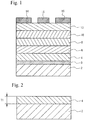
- FIG. 1 is a cross-sectional view of a semiconductor device in accordance with a comparative example.
- an AlN layer 4 is formed on a silicon substrate 2.
- the AlN layer 4 does not include Ga as a composition element and has a Ga impurity concentration of 2 x 10 18 atoms/cm 3 or less.
- a GaN layer 8 is provided on the AlGaN layer 6.
- An AlGaN layer 10 is provided on the GaN layer 8, and a GaN layer 12 is provided on the AlGaN layer 10.
- a source electrode 14, a drain electrode 16 and a gate electrode 18 are provided on the GaN layer 12.
- Each of the source electrodes 14 and the drain electrode 16 is formed by metals of AuGe/Ni/Au in which AuGe is closest to the GaN layer 12.
- the gate electrode 18 is formed by metals of WSi/Ti/Au in which WSi is closest to the GaN layer 12.
- the AlN layer 4 and the AlGaN layer 6 function as buffer layers.
- the GaN layer 8 functions as a channel layer, and the AlGaN layer 10 functions as a supply layer.
- the GaN layer 12 functions as a cap layer.
- the semiconductor device illustrated in Fig. 1 is a HEMT.
- the AlN layer 4 functions as a buffer layer that suppresses diffusion of Ga and prevents Ga in the GaN-based semiconductor layers from diffusing in the silicon substrate 2.
- the semiconductor device of the comparative example has a problem such that a conductive layer 3 is formed in the substrate 2 irrespective of the presence of the buffer layer 4. Thus, a leakage path is formed and the parasitic capacitance is increased. In this case, high-frequency signals may have increasing loss, and the characteristics of the semiconductor device may deteriorate.
- the conductive layer 3 is formed by the following cause.
- the step of forming the AlN layer 4 and the step of forming the GaN-based semiconductor layers are successively carried out.
- the wavers loaded in the MOCVD apparatus are subjected to the steps of forming the AlN layer and forming the GaN-based semiconductor layers, and are removed from the MOCVD apparatus.
- next wafers are loaded in the MOCVD apparatus.
- An impurity that includes Ga may remain in the MOCVD apparatus when the next wafers are subjected to the step of forming the AlN layer 4.
- Ga is taken in during the growth of AlN and may diffuse in the substrate.
- the conductive layer 3 including Ga is formed.
- the residual of the impurity including Ga in the MOCVD apparatus may be restrained by separating the step of forming the AlN layer 4 and the step of forming the GaN-based semiconductor layers from each other. For example, after the step of forming the AlN layer 4 is repeatedly carried out, the step of forming the GaN-based semiconductor layers is carried out.
- Fig. 2 is a cross-sectional view of a sample used in the experiment.
- the AlN layer 4 having a thickness T1 of 300 nm is formed on the substrate 2 made of silicon.
- the AlN layer 4 is grown by the MOCVD method.
- the source material of the AlN layer 4 includes TMA (trimethylaluminum) having a Ga content of 0.1 ppm or less for Al, and NH 3 having a degree of purity of 99.9999% or more.
- the feed rate of TMA is 10 ⁇ mol/min
- the growth temperature is 1050 °C
- the flow rate of NH 3 is 0.5 mol/min
- the growth pressure is 200 torr.
- Sample A is formed by successively forming the AlN layer and the GaN-based semiconductor layers.
- Sample B is formed by separately performing the step of forming the AlN layer and the step of the GaN-based semiconductor layers and by cleaning the MOCVD apparatus between the two steps. The following are the contents and results of the experiment.
- Fig. 3 illustrates a result of the SIMS analysis of the comparative example
- Fig. 4 illustrates a result of the SIMS analysis of a first embodiment, which will be described later.
- the horizontal axis denotes the depth from the surface
- the left-hand side vertical axis denotes the concentration of Ga
- the right-hand side vertical axis denotes secondary ion intensities of Si and Al.
- a region having a high Al concentration (in a depth of 0 to about 0.17 ⁇ m) is the AlN layer 4.
- a region having an almost constant silicon concentration (deeper than 0.17 ⁇ m) is the silicon substrate 2.
- the Ga concentration in the AlN layer 4 is 1 x 10 19 atoms/cm 3 . This may be because the remaining Ga in the MOCVD apparatus is entrapped in, and then diffuses in the AlN layer 4 during growing.
- the Ga concentration in the silicon substrate 2 has the following profile.
- the Ga concentration in the silicon substrate 2 is 1 x 10 17 atoms/cm 3 at the interface between the silicon substrate 2 and the AlN layer 4, and gradually decreases as the distance from the AlN layer 4 increases.
- the profile of gradually decreasing defines a region that functions as the conductive layer 3 (see Fig. 1 ).
- a region having a high Al concentration in a depth of 0 to 0.14 ⁇ m is the AlN layer 4.
- a region having an almost constant silicon concentration (deeper than 0.14 ⁇ m) is the substrate 2.
- the concentration of Ga in the AlN layer 4 is reduced to about 9 x 10 16 atoms/cm 3 .
- the Ga concentration decreases abruptly in the vicinity of the interface between the silicon substrate 2 and the AlN layer 4, and the concentration of Ga in the silicon substrate reduces greatly. This shows that the sample B is improved to have the reduced conductive layer 3 (see Fig. 1 ). It may be understood that the fact that Ga is detected in the AlN layer 4 in Fig. 4 results from a situation in which remaining Ga is mixed in the AlN layer 4 during the step of reducing the quantity of Al.
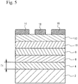
- FIG. 5 is a cross-sectional view of a semiconductor device in accordance with the first embodiment, in which parts that are the same as those illustrated in Fig. 1 are given the same reference numerals.
- the AlN layer 4 is formed on the substrate 2 made of silicon.
- the AlN layer 4 does not include Ga as a composition element and has a Ga impurity concentration of 2 x 10 18 atoms/cm 3 or less.
- the conductive layer 3 (see Fig. 1 ) containing Ga is not formed in the substrate 2.
- FIG. 6 is a flowchart of the method in accordance with the first embodiment.
- the process commences with a step of cleaning the inside of the MOCVD apparatus (step S10).
- steps S10 Examples of the step of cleaning are as follows.
- a reaction tube to which Ga is deposited prior to cleaning is cleaned by etching.
- Parts of the MOCVD apparatus are replaced with new ones.
- Baking is carried out at 1150 °C in the flow of N 2 or O 2 . Baking removes impurities including a group 3 element such as Ga deposited to a jig, chamber and acceptor of the MOCVD apparatus and realizes a condition in which the impurities are removed as much as possible.
- the temperature selected in baking is preferably higher than the temperatures at which the AlN layer 4 and the GaN-based semiconductor layers are grown.
- step S10 a wafer made of silicon is loaded to the MOCVD apparatus that has been cleaned. Then, the AlN layer 4 having the thickness T1 equal to, for example, 300 nm is formed on the wafer.
- the feed rate of TMA at that time is, for example, 10 ⁇ mol/min.
- the AlN layer 4 (first layer) that does not include Ga as a composition element, and has a Ga impurity concentration of 2 x 10 18 atoms/cm 3 or less is formed on the silicon substrate 2 (step S11). Thus, a structure similar to that illustrated in Fig. 2 is obtained.
- step S12 the wafer is removed from the MOCVD apparatus (step S12). That is, the wafer on which the AlN layer 4 is formed as illustrated in Fig. 2 is removed from the MOCVD apparatus. For example, the substrate 2 and the AlN 4 are exposed to the atmosphere.
- step S12 it is determined whether the AlN layer 4 has been formed on a predetermined number N of wafers (step S13). If the answer of step S13 is NO, the process returns to step S11. That is, the step of forming the AlN layer 4 on the silicon substrate 2 is repeatedly carried out.
- step S13 When the answer of step S13 is YES, the process proceeds to step S14 at which the MOCVD apparatus is cleaned as a preprocess.
- the way of cleaning is the same as that employed at step S10.
- the wafer that has been subjected to steps S11 and S12 is loaded to the MOCVD apparatus used at step S11, and the GaN-based semiconductor layers (second layer as a whole) are formed at step S15.
- the second layer includes Ga as a composition element and includes the AlGaN layer 6, the GaN layer 8, the AlGaN layer 10 and the GaN layer 12.
- One of the GaN-based semiconductor layers is formed so as to contact the AlN layer 4.
- the growth condition for each layer is as follows.
- the source material of the AlGaN layer 6 is TMG (trimethylgallium) and TMA.
- the feed rates of TMG and TMA are both 10 ⁇ mol/min, for example.
- the AlGaN layer 6 has a thickness of, for example, 300 nm.
- the source material of the GaN layer 8 is TMG, and the feed rate is, for example, 120 ⁇ mol/min.
- the GaN layer 8 has a thickness of, for example, 1000 nm.
- the source material of the AlGaN layer 10 is TMG and TMA, and the feed rates thereof are, for example, 25 ⁇ mol/min and 5 ⁇ mol/min, respectively.
- the AlGaN layer 10 has a thickness of, for example, 20 nm.
- the source material of the GaN layer 12 is TMG, and the feed rate thereof is, for example, 25 umol/min.
- the GaN layer 12 has a thickness of, for example, 5 nm.
- the growth of the AlN layer 4 uses TMA having a Ga content of 0.1 ppm or less for Al, and NH 3 having a degree of purity of 99.9999% or more.
- the AlN layer 4 has a thickness of, for example, 150 nm.
- step S15 the wafer is removed from the MOCVD apparatus (step S16). Then, it is determined whether the GaN-based semiconductor layers have been formed on a predetermined number N of wafers (step S17). If the answer of step S17 is NO, the process returns to step S15. That is, the step of forming the GaN-based semiconductor layers on the AlN layer 4 is repeatedly carried out.
- step S17 the source electrode 14, the drain electrode 16 and the gate electrode 18 are formed on the GaN layer 12 (step S18). Though the above steps, the semiconductor device of the first embodiment is fabricated.
- the step of forming the AlN layer 4 and the step of forming the GaN-based semiconductor layers are separated from each other. After the step of forming the AlN layer 4 is repeatedly carried out multiple times, the step of the GaN-based semiconductor layers is carried out. It is thus possible to prevent an impurity including Ga from remaining in the MOCVD apparatus prior to the step of forming the AlN layer 4. It is thus possible to restrain entrapment of Ga in the AlN layer 4 during the step of growing the AlN layer 4. Thus, the conductive layer 3 illustrated in Fig. 1 is not formed in the silicon substrate 2.
- the GaN-based semiconductor is a semiconductor that includes Ga and N.
- the GaN-based semiconductor is not limited to GaN and AlGaN described above but includes other semiconductors such as InGaN and InAlGaN.
- the first layer may be a nitride semiconductor other than AlN.
- the nitride semiconductor does not include Ga as a composition element and has a Ga impurity concentration of 2 x 10 18 atoms/cm 3 or less.
- the thickness T1 of the AlN layer 4 is not limited to 300 nm.
- T1 is set equal to 200 nm, the AlN layer 4 can prevent the occurrence of a crack and functions as the buffer layer.
- Fig. 7 is a flowchart of a method for fabricating a semiconductor device in accordance with a second embodiment.
- the process commences with a step of cleaning the inside of the MOCVD apparatus (step S10). This cleaning may be ordinary cleaning prior to growth and is thus different from the cleaning at step S10 in Fig. 6 .
- the AlN layer 4 is grown at step S11 and the wafer is removed from the MOCVD apparatus.
- the steps S11 and S12 are repeatedly carried out until a predetermined number N of wafers has been processed. Steps S12 and S13 in Fig. 7 are the same as those in Fig. 6 .
- step S19 that follows step S12, the wafer is loaded to another MOCVD apparatus that is different from the MOCVD apparatus used at step S11.
- Step S19 is followed by steps S15 - S18 as in the case of Fig. 6 .
- the GaN-based semiconductor layers are grown by the MOCVD apparatus that is different from that used to grow the AlN layer 4.
- the step of forming the AlN layer 4 (step S11) and the step of forming the GaN-based semiconductor layers are carried out separately, and use the different MOCVD apparatuses. It is thus possible to restrain impurities including Ga from being mixed in the MOCVD apparatus and restrain Ga from being entrapped in the AlN layer 4 during the step of growing the AlN layer 4. It is thus possible to depress the forming of the conductive layer including Ga at the interface between the silicon substrate 2 and the AlN layer 4 and to restrain deterioration of the device characteristics.
- the AlN layer 4 and the GaN-based semiconductor layers may be formed concurrently by using the respective MOCVD apparatuses. Thus, speedup of the fabrication process is realized.
- the AlN layer 4 and the GaN-based semiconductor layers may be formed by a method other than the MOCVD method. In order to remove impurities, it is preferable that the MOCVD apparatus used to grow the GaN-based semiconductor layers is cleaned prior to step S15.
- Fig. 8 is a flowchart of a method for fabricating a semiconductor device in accordance with a third embodiment.
- Fig. 9A is a cross-sectional view of a structure of the semiconductor device available after step S11 is performed
- Fig. 9B is a cross-sectional view of a structure of the semiconductor device available after step S18 is performed.
- step S10 an AlN layer 4a (first layer) that does not include Ga as a composition element and a Ga impurity concentration of 2 x 10 18 atoms/cm 3 or less is formed on the silicon substrate 2 (step S11).
- the AlN layer 4a has a thickness T2 of, for example, 150 nm, which may be half the thickness T1 of the AlN layer obtained in the complete semiconductor device (see Fig. 5 and Fig. 9B ).
- step S11 the wafer on which the AlN layer 4a is formed as illustrated in Fig. 9A is removed from the MOCVD apparatus (step S12). For example, the silicon substrate 2 and the AlN layer 4a are exposed to the atmosphere. Then, steps S13 and S14 are carried out. Steps S10 through S14 are the same as those illustrated in Fig. 6 .
- an AlN layer 4b (third layer) is formed on the AlN layer 4a (step S20) so as to contact the AlN layer 4a.
- the AlN layer 4b has a thickness T3 of, for example, 150 nm, and does not include Ga as a composition element.
- the AlN layer 4b has a Ga impurity concentration of 2 x 10 18 atoms/cm 3 or less.
- the GaN-based semiconductor layers are formed on the AlN layer 4b (step S15).
- Steps S16 through S18 that follow step S15 are the same as those illustrated in Fig. 6 .
- the semiconductor device illustrated in Fig. 9B is completed.
- the AlN layers 4a and 4b form the AlN layer 4 having a thickness T1 of, for example, 300 nm.
- the conditions for growing the layers are as follows.
- the source material of the AlN layer 4a and that of the AlN layer 4b are TMA, and the feed rate thereof is 10 ⁇ mol/min.
- Each of the AlN layers 4a and 4b is 150 nm thick, for example.
- the source material of the AlGaN layer 6 is TMG and TMA, and the feed rates thereof are 10 ⁇ mol/min.
- the thickness of the AlGaN layer 6 is, for example, 300 nm.
- the source material of the GaN layer 8 is TMG, and the feed rate thereof is, for example, 120 ⁇ mol/min.
- the GaN layer 8 is 1000 nm thick, for example.
- the source material of the AlGaN layer 10 is TMG and TMA, and the feed rates thereof are 25 ⁇ mol/min and 5 ⁇ mol/min, respectively.
- the AlGaN layer 10 is 20 nm thick, for example.
- the source material of the GaN layer 12 is TMG, and the feed rate thereof is 25 ⁇ mol/min.
- the GaN layer 12 is 5 nm thick, for example.
- the GaN layer 12 has a thickness of, for example, 5 nm.
- the growth of the AlN layer 4 uses TMA having a Ga content of 0.1 ppm or less for Al, and NH 3 having a degree of purity of 99.9999% or more.
- the AlN layer 4 has a thickness of, for example, 150 nm.
- the step of forming the AlN layer 4a (step S11) and the step of forming the GaN-based semiconductor layers (step S15) are separated from each other, as in the case of the first embodiment.
- the step of the GaN-based semiconductor layers is carried out. It is thus possible to prevent an impurity including Ga from remaining in the MOCVD. It is thus possible to prevent the conductive layer 3 including Ga from being formed at the interface between the silicon substrate 2 and the AlN layer 4 and illustrated in Fig. 1 is not formed in the silicon substrate 2.
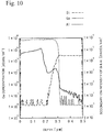
- Fig. 10 is a graph that illustrates a result of the SIMS analysis of the third embodiment in the state in which the growth of the AlN layer 4b is completed.
- a region having a high Ga concentration in a depth of 0 to 0.17 ⁇ m is the AlN layer 4b, and another region having a decreasing Ga concentration in a depth of 0.17 to 0.3 ⁇ m is the AlN layer 4a.
- a further region having an almost constant silicon concentration (deeper than 0.3 ⁇ m) is the silicon substrate 2.
- the Ga concentration in the AlN layer 4b is approximately 1 x 10 19 atoms/cm 3
- the Ga concentration in the AlN layer 4a is approximately 2 x 10 17 atoms/cm 3
- the Ga concentration in the vicinity of the interface between the silicon substrate 2 and eth AlN layer 4a is approximately 1 x 10 16 atoms/cm 3 , and decreases abruptly in the depth direction. Since the AlN layer 4b is grown by the MOCVD apparatus used to grow the layers including Ga, the Ga concentration is relatively high. However, the Ga concentration in the AlN layer 4a is decreased. Thus, it may be understood that the AlN layer 4a functions to restrain the diffusion of Ga.
- the AlN layer 4a that is thinner than the AlN layer 4 in the complete semiconductor device, and is then removed from the MOCVD apparatus (steps S11 and S12).
- the step of forming the AlN layer 4b and the step of forming the GAN-based semiconductor layers are successively carried out.
- the AlN layer 4b is formed, and the GaN-based semiconductor layers are formed without the silicon substrate 2 and the AlN layer 4b being exposed to the atmosphere. It is thus possible to restrain warpage or crack from occurring in the AlN layer 4.
- the AlN layer 4b is formed on the AlN layer 4a (step S20).
- the AlN layer having a sufficient thickness that enables the AlN layer to function as the buffer layer is formed on the silicon substrate 2.
- the third layer is not limited to the AlN layer but may be anther nitride semiconductor that does not include Ga as a composition element.
- the thickness T2 of the AlN layer 4a is not limited to 150 nm. In terms of suppression of crack, it is preferable to use a thinner AlN layer. For example, when the thickness T2 is 100 nm or less, it is possible to more effectively suppress crack. More particularly, the thickness T2 is 50 nm or less.
- the thickness T2 is set equal to or more than 10 nm.
- the thickness T3 of the AlN layer 4b is not limited to 150 nm in the foregoing, it may be changed appropriately taking the thickness T2 of the AlN layer 4a into consideration.
- the thickness T3 is preferably more than 150 nm. When the thickness T3 is 200 nm or more, the buffer layer having a sufficient thickness is available.
- the third embodiment may be varied so that the step of forming the AlN layer 4a and the step of forming the GaN-based layers are carried out by the separate MOCVD apparatuses.
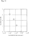
- Fig. 11 is a graph that illustrates a result of gain evaluation of the semiconductor device configured in accordance with the first embodiment.
- the substrates are prepared by changing the degree of cleaning (step S10 in Fig. 6 ) and changing the concentration of Ga in the AlN layer 4.
- the semiconductor layers and the electrodes are formed.
- the gains of the semiconductor devices thus prepared are measured.
- the horizontal axis denotes the concentration of Ga in the AlN layer 4
- the vertical axis denotes a relative gain obtained by normalizing the gain with respect to the gain of the comparative example (see Fig. 1 ).
- the gain of the first embodiment is about 1 dB better than that of the comparative example.
- the concentration of Ga in the AlN layer 4 is equal to or close to 5 x 10 17 atoms/cm 3
- the gain of the first embodiment is about 2 dB better than that of the comparative example.
- the concentration of Ga in the AlN layer 4 is equal to or close to 1 x 10 17 atoms/cm 3
- the gain of the first embodiment is about 3 dB better than that of the comparative example.
- the Ga concentration is preferably set equal to or less than 2 x 10 18 atoms/cm 3 in order to obtain an improvement equal to or more than 1 dB with respect to the comparative example.
- the impurity of the source material of Al used to grow the AlN layer is equal to or less than 2 ppm in order to form the AlN layer 4 by the MOCVD method.
- the content of Ga to Al in the organic source material of Al used in the MBE method is equal to or less than 40 ppm.
- the concentration of Ga in the AlN layer 4 is set approximately equal to 5 x 10¹⁷ atoms/cm3 and the MOCVD method is employed, it is preferable that the content of Ga to Al in the organic source material of Al is equal to or less than 0.5 ppm.
- the content of Ga to Al of the source material is preferably equal to or less than 10 ppm.
- the concentration of Ga in the AlN layer 4 is set approximately equal to 1 x 10¹⁷ atoms/cm3 and the MOCVD method is employed, it is preferable that the content of Ga to Al in the organic source material of Al is equal to or less than 0.1 ppm.
- the content of Ga to Al of the source material is preferably equal to or less than 2 ppm.
- the semiconductor devices of the above-described embodiments are not limited to HEMTs but may be FETs.
- high-frequency devices configured in accordance with the aspects of the present invention are capable of restraining deterioration of the characteristics due to leakage path or parasitic capacitance.
- the method for growing the layers is not limited to MOCVD and MBE but may be HVPE, which use the MOCVD apparatus, the MBE apparatus and the HVPE apparatus, respectively.
Description
- The present invention relates to a method for fabricating a semiconductor device, and more particularly, to a method for fabricating a semiconductor device having a semiconductor layer that includes gallium (Ga) and is formed on a silicon (Si) substrate by a vapor deposition method.
- A semiconductor device using a nitride semiconductor layer including Ga (gallium) as a composition element (GaN-based semiconductor layer) has attracted attention as devices capable of operating at high frequencies. An example of such a semiconductor device is a HEMT (High Electron Mobility Transistor). This type of semiconductor device frequently employs a silicon carbide (SiC) substrate or a sapphire substrate. Since these substrates are expensive, it is desired to develop a method for forming a semiconductor device havin a GaN-based semiconductor layer on the silicon substrate. An MBE (Molecular Beam Epitaxy) method grows layers under high vacuum and has a difficulty in handling a source material of nitrogen. In contrast, an MOCVD (Metal Organic Chemical Vapor Deposition) method grows layers under reduced pressure or ordinary pressure, and handles NH3 and NH2 as a source material of nitrogen easily. Thus, the MOCVD method is widely used to grow GaN-based semiconductors, Japanese Laid-Open Patent Publication No.
2004-524250 -
JP 2009/007205 -
WO 2008/048303 discloses a method for forming a bulk crystal structure, the method including depositing an epitaxial AlN layer on a single-crystal substrate, growing a GaN nucleation layer on the AlN-coated substrate by HVPE, growing a GaN transitional layer on the nucleation layer by HVPE, and growing a GaN bulk layer on the transitional layer by HVPE. - It is desirable to provide a method for fabricating a semiconductor device capable of restraining a deterioration of the semiconductor device due to an unwanted conductive layer containing Ga.
- In an example, there is provided a method for fabricating a semiconductor device including: cleaning an apparatus used to grow a layer including Ga; performing a first step of forming a first
layer on a plurality of substrates made of silicon by using the apparatus, the first layer including a nitride semiconductor that does not include Ga as a composition element and has a Ga impurity concentration of 2 x 10¹⁸ atoms/cm3 or less; and then performing a second step of forming a second layer on the first layer, on the plurality of substrates, by using the apparatus, the second layer including a nitride semiconductor including Ga. - In another example, there is provided a method for fabricating a semiconductor device including: performing a first step of forming a first layer on a substrate made of silicon by using an apparatus, the first layer including a nitride semiconductor that does not include Ga as a composition element and that has a Ga impurity concentration of 2 x 10¹⁸ atoms/cm3 or less; performing a second step of forming a second layer on the first layer by using another apparatus, the second layer including a nitride semiconductor including Ga,
the method further comprising performing a third step of forming a third layer on the first layer by using the apparatus after the first step is carried out and before the second step is carried out, the third layer being formed from a nitride semiconductor having a Ga impurity concentration of 2 x 10¹⁸ atoms/cm3 or less, wherein the second step and the third step are successively carried out, and the second layer is formed on the third layer. -
Fig. 1 is a cross-sectional view of a semiconductor device in accordance with a comparative example; -
Fig. 2 is a cross-sectional view of a sample used in an experiment; -
Fig. 3 illustrates a result of a SIMS analysis of sample A; -
Fig. 4 illustrates a result of a SIMS analysis of sample B; -
Fig. 5 is a cross-sectional view of a semiconductor device in accordance with a first embodiment outside the invention; -
Fig. 6 is a flowchart describing a method for fabricating the semiconductor device in accordance with the first embodiment outside the invention; -
Fig. 7 is a flowchart describing a method for fabricating a semiconductor device in accordance with a second embodiment outside the invention; -
Fig. 8 is a flowchart describing a method for fabricating a semiconductor device in accordance with a third embodiment part of the invention; -
Figs. 9A and 9B are cross-sectional views of the semiconductor device in accordance with the third embodiment part of the invention ; -
Fig. 10 illustrates a result of a SIMS analysis of the third embodiment; and -
Fig. 11 illustrates a result of gain evaluation of semiconductor devices. - An embodiment of the present invention is made taking the following into consideration. In a case where a GaN-based semiconductor is grown on the silicon substrate by a vapor deposition method such as MOCVD or HVPE (Hydride Vapor Phase Epitaxy), a high growth temperature of 900 °C or more is used. Such a high temperature is different from that used in growth by MBE or growth of a GaAs-based semiconductor. The high growth temperature causes Ga to easily diffuse in the silicon substrate. The diffused Ga may form a conductive layer in the silicon substrate. The conductive layer increases the parasitic capacitance and increases the loss of high-frequency signals. Thus, the semiconductor device has deteriorated characteristics.
- According to an aspect of the embodiment, it is possible to restrain the conductive layer from being formed in the silicon substrate and to prevent the characteristics of the semiconductor device from being deteriorated.
- Now, a comparative example is described.
Fig. 1 is a cross-sectional view of a semiconductor device in accordance with a comparative example. - Referring to
Fig. 1 , anAlN layer 4 is formed on asilicon substrate 2. TheAlN layer 4 does not include Ga as a composition element and has a Ga impurity concentration of 2 x 10¹⁸ atoms/cm3 or less. An AlGaNlayer 6, which is a nitride semiconductor including Ga as a composition element, is formed on theAlN layer 4. A GaNlayer 8 is provided on the AlGaNlayer 6. An AlGaNlayer 10 is provided on the GaNlayer 8, and aGaN layer 12 is provided on the AlGaNlayer 10. Asource electrode 14, adrain electrode 16 and agate electrode 18 are provided on theGaN layer 12. Each of thesource electrodes 14 and thedrain electrode 16 is formed by metals of AuGe/Ni/Au in which AuGe is closest to theGaN layer 12. Thegate electrode 18 is formed by metals of WSi/Ti/Au in which WSi is closest to the GaNlayer 12. - The
AlN layer 4 and the AlGaNlayer 6 function as buffer layers. The GaNlayer 8 functions as a channel layer, and the AlGaNlayer 10 functions as a supply layer. The GaNlayer 12 functions as a cap layer. The semiconductor device illustrated inFig. 1 is a HEMT. TheAlN layer 4 functions as a buffer layer that suppresses diffusion of Ga and prevents Ga in the GaN-based semiconductor layers from diffusing in thesilicon substrate 2. - However, the semiconductor device of the comparative example has a problem such that a
conductive layer 3 is formed in thesubstrate 2 irrespective of the presence of thebuffer layer 4. Thus, a leakage path is formed and the parasitic capacitance is increased. In this case, high-frequency signals may have increasing loss, and the characteristics of the semiconductor device may deteriorate. Theconductive layer 3 is formed by the following cause. - In the process of fabricating the semiconductor device of the comparative example, the step of forming the
AlN layer 4 and the step of forming the GaN-based semiconductor layers are successively carried out. Thus, in a case where the MOCVD growing step is repeatedly applied to multiple wafers, the wavers loaded in the MOCVD apparatus are subjected to the steps of forming the AlN layer and forming the GaN-based semiconductor layers, and are removed from the MOCVD apparatus. Then, next wafers are loaded in the MOCVD apparatus. An impurity that includes Ga may remain in the MOCVD apparatus when the next wafers are subjected to the step of forming theAlN layer 4. In this case, Ga is taken in during the growth of AlN and may diffuse in the substrate. Thus, theconductive layer 3 including Ga is formed. - The residual of the impurity including Ga in the MOCVD apparatus may be restrained by separating the step of forming the
AlN layer 4 and the step of forming the GaN-based semiconductor layers from each other. For example, after the step of forming theAlN layer 4 is repeatedly carried out, the step of forming the GaN-based semiconductor layers is carried out. - A description will now be given of an experiment conducted by the inventors.
Fig. 2 is a cross-sectional view of a sample used in the experiment. - Referring to
Fig. 2 , theAlN layer 4 having a thickness T1 of 300 nm is formed on thesubstrate 2 made of silicon. TheAlN layer 4 is grown by the MOCVD method. The source material of theAlN layer 4 includes TMA (trimethylaluminum) having a Ga content of 0.1 ppm or less for Al, and NH3 having a degree of purity of 99.9999% or more. The feed rate of TMA is 10 µmol/min, the growth temperature is 1050 °C, the flow rate of NH3 is 0.5 mol/min, and the growth pressure is 200 torr. F - The experiment uses two types of samples. Sample A is formed by successively forming the AlN layer and the GaN-based semiconductor layers. Sample B is formed by separately performing the step of forming the AlN layer and the step of the GaN-based semiconductor layers and by cleaning the MOCVD apparatus between the two steps. The following are the contents and results of the experiment.
- In the experiment, the samples A and B were subjected to a SIMS (Secondary Ion Mass Spectrometry) analysis.
Fig. 3 illustrates a result of the SIMS analysis of the comparative example, andFig. 4 illustrates a result of the SIMS analysis of a first embodiment, which will be described later. InFigs. 3 and4 , the horizontal axis denotes the depth from the surface, the left-hand side vertical axis denotes the concentration of Ga, and the right-hand side vertical axis denotes secondary ion intensities of Si and Al. - Referring to
Fig. 3 , a region having a high Al concentration (in a depth of 0 to about 0.17 µm) is theAlN layer 4. A region having an almost constant silicon concentration (deeper than 0.17 µm) is thesilicon substrate 2. As illustrated inFig. 3 , the Ga concentration in theAlN layer 4 is 1 x 10¹⁹ atoms/cm3. This may be because the remaining Ga in the MOCVD apparatus is entrapped in, and then diffuses in theAlN layer 4 during growing. The Ga concentration in thesilicon substrate 2 has the following profile. The Ga concentration in thesilicon substrate 2 is 1 x 10¹⁷atoms/cm3 at the interface between thesilicon substrate 2 and theAlN layer 4, and gradually decreases as the distance from theAlN layer 4 increases. The profile of gradually decreasing defines a region that functions as the conductive layer 3 (seeFig. 1 ). - Referring to
Fig. 4 , a region having a high Al concentration (in a depth of 0 to 0.14 µm) is theAlN layer 4. A region having an almost constant silicon concentration (deeper than 0.14 µm) is thesubstrate 2. As illustrated inFig. 4 , the concentration of Ga in theAlN layer 4 is reduced to about 9 x 10¹⁶ atoms/cm3. The Ga concentration decreases abruptly in the vicinity of the interface between thesilicon substrate 2 and theAlN layer 4, and the concentration of Ga in the silicon substrate reduces greatly. This shows that the sample B is improved to have the reduced conductive layer 3 (seeFig. 1 ). It may be understood that the fact that Ga is detected in theAlN layer 4 inFig. 4 results from a situation in which remaining Ga is mixed in theAlN layer 4 during the step of reducing the quantity of Al. - As described above, forming of the
AlN layer 4 on the silicon substrate using the growth apparatus from which Ga has been removed brings about the effect of reducing the concentration of Ga in theAlN layer 4 and restrains forming of theconductive layer 3. - Embodiments of the present invention are now described with reference to the accompanying drawings.
- A semiconductor device in accordance with the first embodiment is now described.
Fig. 5 is a cross-sectional view of a semiconductor device in accordance with the first embodiment, in which parts that are the same as those illustrated inFig. 1 are given the same reference numerals. - Referring to
Fig. 5 , theAlN layer 4 is formed on thesubstrate 2 made of silicon. TheAlN layer 4 does not include Ga as a composition element and has a Ga impurity concentration of 2 x 10¹⁸ atoms/cm3 or less. TheAlGaN layer 6, which is a nitride semiconductor having Ga as a composition element, is formed on theAlN layer 4. The conductive layer 3 (seeFig. 1 ) containing Ga is not formed in thesubstrate 2. - A description is now given of a method for fabricating the semiconductor device in accordance with the first embodiment.
Fig. 6 is a flowchart of the method in accordance with the first embodiment. - Referring to
Fig. 6 , the process commences with a step of cleaning the inside of the MOCVD apparatus (step S10). Examples of the step of cleaning are as follows. A reaction tube to which Ga is deposited prior to cleaning is cleaned by etching. Parts of the MOCVD apparatus are replaced with new ones. Baking is carried out at 1150 °C in the flow of N2 or O2. Baking removes impurities including agroup 3 element such as Ga deposited to a jig, chamber and acceptor of the MOCVD apparatus and realizes a condition in which the impurities are removed as much as possible. The temperature selected in baking is preferably higher than the temperatures at which theAlN layer 4 and the GaN-based semiconductor layers are grown. - After step S10, a wafer made of silicon is loaded to the MOCVD apparatus that has been cleaned. Then, the
AlN layer 4 having the thickness T1 equal to, for example, 300 nm is formed on the wafer. The feed rate of TMA at that time is, for example, 10 µmol/min. In other words, the AlN layer 4 (first layer) that does not include Ga as a composition element, and has a Ga impurity concentration of 2 x 10¹⁸ atoms/cm3 or less is formed on the silicon substrate 2 (step S11). Thus, a structure similar to that illustrated inFig. 2 is obtained. - After step S11, the wafer is removed from the MOCVD apparatus (step S12). That is, the wafer on which the
AlN layer 4 is formed as illustrated inFig. 2 is removed from the MOCVD apparatus. For example, thesubstrate 2 and theAlN 4 are exposed to the atmosphere. - After step S12, it is determined whether the
AlN layer 4 has been formed on a predetermined number N of wafers (step S13). If the answer of step S13 is NO, the process returns to step S11. That is, the step of forming theAlN layer 4 on thesilicon substrate 2 is repeatedly carried out. - When the answer of step S13 is YES, the process proceeds to step S14 at which the MOCVD apparatus is cleaned as a preprocess. The way of cleaning is the same as that employed at step S10.
- After step S14, the wafer that has been subjected to steps S11 and S12 is loaded to the MOCVD apparatus used at step S11, and the GaN-based semiconductor layers (second layer as a whole) are formed at step S15. The second layer includes Ga as a composition element and includes the
AlGaN layer 6, theGaN layer 8, theAlGaN layer 10 and theGaN layer 12. One of the GaN-based semiconductor layers is formed so as to contact theAlN layer 4. The growth condition for each layer is as follows. - The source material of the
AlGaN layer 6 is TMG (trimethylgallium) and TMA. The feed rates of TMG and TMA are both 10 µmol/min, for example. TheAlGaN layer 6 has a thickness of, for example, 300 nm. The source material of theGaN layer 8 is TMG, and the feed rate is, for example, 120 µmol/min. TheGaN layer 8 has a thickness of, for example, 1000 nm. The source material of theAlGaN layer 10 is TMG and TMA, and the feed rates thereof are, for example, 25 µmol/min and 5 µmol/min, respectively. TheAlGaN layer 10 has a thickness of, for example, 20 nm. The source material of theGaN layer 12 is TMG, and the feed rate thereof is, for example, 25 umol/min. TheGaN layer 12 has a thickness of, for example, 5 nm. The growth of theAlN layer 4 uses TMA having a Ga content of 0.1 ppm or less for Al, and NH3 having a degree of purity of 99.9999% or more. TheAlN layer 4 has a thickness of, for example, 150 nm. - After step S15, the wafer is removed from the MOCVD apparatus (step S16). Then, it is determined whether the GaN-based semiconductor layers have been formed on a predetermined number N of wafers (step S17). If the answer of step S17 is NO, the process returns to step S15. That is, the step of forming the GaN-based semiconductor layers on the
AlN layer 4 is repeatedly carried out. - After step S17, the
source electrode 14, thedrain electrode 16 and thegate electrode 18 are formed on the GaN layer 12 (step S18). Though the above steps, the semiconductor device of the first embodiment is fabricated. - According to the first embodiment, as illustrated in
Fig. 6 , the step of forming theAlN layer 4 and the step of forming the GaN-based semiconductor layers are separated from each other. After the step of forming theAlN layer 4 is repeatedly carried out multiple times, the step of the GaN-based semiconductor layers is carried out. It is thus possible to prevent an impurity including Ga from remaining in the MOCVD apparatus prior to the step of forming theAlN layer 4. It is thus possible to restrain entrapment of Ga in theAlN layer 4 during the step of growing theAlN layer 4. Thus, theconductive layer 3 illustrated inFig. 1 is not formed in thesilicon substrate 2. - It is possible to restrain entrapment of
group 3 element other than Ga in theAlN layer 4. It is thus possible to keep the resistance of thesilicon substrate 2 high and prevent the characteristics of the semiconductor device from being deteriorated. - The GaN-based semiconductor is a semiconductor that includes Ga and N. The GaN-based semiconductor is not limited to GaN and AlGaN described above but includes other semiconductors such as InGaN and InAlGaN. The first layer may be a nitride semiconductor other than AlN. The nitride semiconductor does not include Ga as a composition element and has a Ga impurity concentration of 2 x 10¹⁸ atoms/cm3 or less.
- The thickness T1 of the
AlN layer 4 is not limited to 300 nm. For example, when T1 is set equal to 200 nm, theAlN layer 4 can prevent the occurrence of a crack and functions as the buffer layer. -
Fig. 7 is a flowchart of a method for fabricating a semiconductor device in accordance with a second embodiment. - Referring to
Fig. 7 , the process commences with a step of cleaning the inside of the MOCVD apparatus (step S10). This cleaning may be ordinary cleaning prior to growth and is thus different from the cleaning at step S10 inFig. 6 . Next, theAlN layer 4 is grown at step S11 and the wafer is removed from the MOCVD apparatus. At step S13, the steps S11 and S12 are repeatedly carried out until a predetermined number N of wafers has been processed. Steps S12 and S13 inFig. 7 are the same as those inFig. 6 . - At step S19 that follows step S12, the wafer is loaded to another MOCVD apparatus that is different from the MOCVD apparatus used at step S11. Step S19 is followed by steps S15 - S18 as in the case of
Fig. 6 . The GaN-based semiconductor layers are grown by the MOCVD apparatus that is different from that used to grow theAlN layer 4. - According to the second embodiment, the step of forming the AlN layer 4 (step S11) and the step of forming the GaN-based semiconductor layers are carried out separately, and use the different MOCVD apparatuses. It is thus possible to restrain impurities including Ga from being mixed in the MOCVD apparatus and restrain Ga from being entrapped in the
AlN layer 4 during the step of growing theAlN layer 4. It is thus possible to depress the forming of the conductive layer including Ga at the interface between thesilicon substrate 2 and theAlN layer 4 and to restrain deterioration of the device characteristics. - The
AlN layer 4 and the GaN-based semiconductor layers may be formed concurrently by using the respective MOCVD apparatuses. Thus, speedup of the fabrication process is realized. TheAlN layer 4 and the GaN-based semiconductor layers may be formed by a method other than the MOCVD method. In order to remove impurities, it is preferable that the MOCVD apparatus used to grow the GaN-based semiconductor layers is cleaned prior to step S15. -
Fig. 8 is a flowchart of a method for fabricating a semiconductor device in accordance with a third embodiment.Fig. 9A is a cross-sectional view of a structure of the semiconductor device available after step S11 is performed, andFig. 9B is a cross-sectional view of a structure of the semiconductor device available after step S18 is performed. - Referring to
Fig. 8 , after step S10 is carried out, anAlN layer 4a (first layer) that does not include Ga as a composition element and a Ga impurity concentration of 2 x 10¹⁸ atoms/cm3 or less is formed on the silicon substrate 2 (step S11). - Referring to
Fig. 9A , theAlN layer 4a has a thickness T2 of, for example, 150 nm, which may be half the thickness T1 of the AlN layer obtained in the complete semiconductor device (seeFig. 5 andFig. 9B ). - After step S11, the wafer on which the
AlN layer 4a is formed as illustrated inFig. 9A is removed from the MOCVD apparatus (step S12). For example, thesilicon substrate 2 and theAlN layer 4a are exposed to the atmosphere. Then, steps S13 and S14 are carried out. Steps S10 through S14 are the same as those illustrated inFig. 6 . - After step S14, an
AlN layer 4b (third layer) is formed on theAlN layer 4a (step S20) so as to contact theAlN layer 4a. TheAlN layer 4b has a thickness T3 of, for example, 150 nm, and does not include Ga as a composition element. TheAlN layer 4b has a Ga impurity concentration of 2 x 10¹⁸ atoms/cm3 or less. - After the step S20, the GaN-based semiconductor layers are formed on the
AlN layer 4b (step S15). Steps S16 through S18 that follow step S15 are the same as those illustrated inFig. 6 . Through the above-described steps, the semiconductor device illustrated inFig. 9B is completed. The AlN layers 4a and 4b form theAlN layer 4 having a thickness T1 of, for example, 300 nm. The conditions for growing the layers are as follows. - The source material of the
AlN layer 4a and that of theAlN layer 4b are TMA, and the feed rate thereof is 10 µmol/min. Each of the AlN layers 4a and 4b is 150 nm thick, for example. The source material of theAlGaN layer 6 is TMG and TMA, and the feed rates thereof are 10 µmol/min. The thickness of theAlGaN layer 6 is, for example, 300 nm. The source material of theGaN layer 8 is TMG, and the feed rate thereof is, for example, 120 µmol/min. TheGaN layer 8 is 1000 nm thick, for example. The source material of theAlGaN layer 10 is TMG and TMA, and the feed rates thereof are 25 µmol/min and 5 µmol/min, respectively. TheAlGaN layer 10 is 20 nm thick, for example. The source material of theGaN layer 12 is TMG, and the feed rate thereof is 25 µmol/min. TheGaN layer 12 is 5 nm thick, for example. TheGaN layer 12 has a thickness of, for example, 5 nm. The growth of theAlN layer 4 uses TMA having a Ga content of 0.1 ppm or less for Al, and NH3 having a degree of purity of 99.9999% or more. TheAlN layer 4 has a thickness of, for example, 150 nm. - According to an embodiment outside the invention, the step of forming the
AlN layer 4a (step S11) and the step of forming the GaN-based semiconductor layers (step S15) are separated from each other, as in the case of the first embodiment. After the step of forming theAlN layer 4a is repeatedly carried out multiple times, the step of the GaN-based semiconductor layers is carried out. It is thus possible to prevent an impurity including Ga from remaining in the MOCVD. It is thus possible to prevent theconductive layer 3 including Ga from being formed at the interface between thesilicon substrate 2 and theAlN layer 4 and illustrated inFig. 1 is not formed in thesilicon substrate 2. -
Fig. 10 is a graph that illustrates a result of the SIMS analysis of the third embodiment in the state in which the growth of theAlN layer 4b is completed. A region having a high Ga concentration in a depth of 0 to 0.17 µm is theAlN layer 4b, and another region having a decreasing Ga concentration in a depth of 0.17 to 0.3 µm is theAlN layer 4a. A further region having an almost constant silicon concentration (deeper than 0.3 µm) is thesilicon substrate 2. - As illustrated in
Fig. 10 , the Ga concentration in theAlN layer 4b is approximately 1 x 10¹⁹ atoms/cm3, while the Ga concentration in theAlN layer 4a is approximately 2 x 10¹⁷ atoms/cm3. The Ga concentration in the vicinity of the interface between thesilicon substrate 2 andeth AlN layer 4a is approximately 1 x 10¹⁶ atoms/cm3, and decreases abruptly in the depth direction. Since theAlN layer 4b is grown by the MOCVD apparatus used to grow the layers including Ga, the Ga concentration is relatively high. However, the Ga concentration in theAlN layer 4a is decreased. Thus, it may be understood that theAlN layer 4a functions to restrain the diffusion of Ga. - It is to be noted that there is a difference in thermal expansion coefficient between the
silicon substrate 2 and theAlN layer 4. If theAlN layer 4 is too thick, thesilicon substrate 2 may be warped and theAlN layer 4 may crack when the wafer is removed from the MOCVD apparatus and thesilicon substrate 2 and theAlN layer 4 are exposed to the atmosphere. - According to the third embodiment, the
AlN layer 4a that is thinner than theAlN layer 4 in the complete semiconductor device, and is then removed from the MOCVD apparatus (steps S11 and S12). The step of forming theAlN layer 4b and the step of forming the GAN-based semiconductor layers are successively carried out. For example, theAlN layer 4b is formed, and the GaN-based semiconductor layers are formed without thesilicon substrate 2 and theAlN layer 4b being exposed to the atmosphere. It is thus possible to restrain warpage or crack from occurring in theAlN layer 4. - After the
AlN layer 4a is formed, theAlN layer 4b is formed on theAlN layer 4a (step S20). Thus, the AlN layer having a sufficient thickness that enables the AlN layer to function as the buffer layer is formed on thesilicon substrate 2. The third layer is not limited to the AlN layer but may be anther nitride semiconductor that does not include Ga as a composition element. The thickness T2 of theAlN layer 4a is not limited to 150 nm. In terms of suppression of crack, it is preferable to use a thinner AlN layer. For example, when the thickness T2 is 100 nm or less, it is possible to more effectively suppress crack. More particularly, the thickness T2 is 50 nm or less. In case where theAlN layer 4a is too thin, there is a difficulty in growing theAlN layer 4a. Thus, it is preferable to set the thickness T2 equal to or more than 10 nm. Although the thickness T3 of theAlN layer 4b is not limited to 150 nm in the foregoing, it may be changed appropriately taking the thickness T2 of theAlN layer 4a into consideration. In order to enable theAlN layer 4 to function as the buffer layer, the thickness T3 is preferably more than 150 nm. When the thickness T3 is 200 nm or more, the buffer layer having a sufficient thickness is available. - As in the case of the second embodiment, the third embodiment may be varied so that the step of forming the
AlN layer 4a and the step of forming the GaN-based layers are carried out by the separate MOCVD apparatuses. -
Fig. 11 is a graph that illustrates a result of gain evaluation of the semiconductor device configured in accordance with the first embodiment. In the gain evaluation, several semiconductor devices having the following different substrates are prepared. The substrates are prepared by changing the degree of cleaning (step S10 inFig. 6 ) and changing the concentration of Ga in theAlN layer 4. On the different substrates, the semiconductor layers and the electrodes are formed. Then, the gains of the semiconductor devices thus prepared are measured. InFig. 11 , the horizontal axis denotes the concentration of Ga in theAlN layer 4, and the vertical axis denotes a relative gain obtained by normalizing the gain with respect to the gain of the comparative example (seeFig. 1 ). - As illustrated in
Fig. 11 , when the concentration of Ga in theAlN layer 4 is equal to or close to 2 x 10¹⁸ atoms/cm3, the gain of the first embodiment is about 1 dB better than that of the comparative example. Similarly, when the concentration of Ga in theAlN layer 4 is equal to or close to 5 x 10¹⁷ atoms/cm3, the gain of the first embodiment is about 2 dB better than that of the comparative example. When the concentration of Ga in theAlN layer 4 is equal to or close to 1 x 10¹⁷ atoms/cm3, the gain of the first embodiment is about 3 dB better than that of the comparative example. It can be seen that the Ga concentration is preferably set equal to or less than 2 x 10¹⁸ atoms/cm3 in order to obtain an improvement equal to or more than 1 dB with respect to the comparative example. - In order to realize a Ga concentration of 2 x 10¹⁸ atoms/cm3 or less, the impurity of the source material of Al used to grow the AlN layer. It is preferable that the content of Ga to Al in the organic source material of Al such as TMA is equal to or less than 2 ppm in order to form the
AlN layer 4 by the MOCVD method. In order to form theAlN layer 4 by the MBE method, it is preferable that the content of Ga to Al in the organic source material of Al used in the MBE method is equal to or less than 40 ppm. - In a case where the concentration of Ga in the
AlN layer 4 is set approximately equal to 5 x 10¹⁷ atoms/cm3 and the MOCVD method is employed, it is preferable that the content of Ga to Al in the organic source material of Al is equal to or less than 0.5 ppm. When the MBE method is employed, the content of Ga to Al of the source material is preferably equal to or less than 10 ppm. - In a case where the concentration of Ga in the
AlN layer 4 is set approximately equal to 1 x 10¹⁷ atoms/cm3 and the MOCVD method is employed, it is preferable that the content of Ga to Al in the organic source material of Al is equal to or less than 0.1 ppm. When the MBE method is employed, the content of Ga to Al of the source material is preferably equal to or less than 2 ppm. - The semiconductor devices of the above-described embodiments are not limited to HEMTs but may be FETs. Particularly, high-frequency devices configured in accordance with the aspects of the present invention are capable of restraining deterioration of the characteristics due to leakage path or parasitic capacitance. The method for growing the layers is not limited to MOCVD and MBE but may be HVPE, which use the MOCVD apparatus, the MBE apparatus and the HVPE apparatus, respectively.
- The present invention is not limited to the specifically described embodiments and embodiments, but may include other embodiments and variations without departing from the scope of the present invention.
Claims (8)
- A method for fabricating a semiconductor device comprising:performing a first step of forming a first layer (4a) on a substrate (2) made of silicon by using an apparatus, the first layer (4a) including a nitride semiconductor that does not include Ga as a composition element; andperforming a second step of forming a second layer (6, 8, 10, 12) on the first layer (4a) by using another apparatus, the second layer including a nitride semiconductor including Ga,wherein:
the nitride semiconductor of the first layer has a Ga impurity concentration of 2 x 10¹⁸ atoms/cm3 or less, wherein the method further comprises performing a third step of forming a third layer (4b) on the first layer (4a) by using the apparatus after the first step is carried out and before the second step is carried out, the third layer including a nitride semiconductor that does not include Ga as a composition element, wherein the third step and the second step are successively carried out, and the second layer (6, 8, 10, 12) is formed on the third layer (4b). - The method according to claim 1, wherein the third layer (4b) is made of composition elements identical to those of the first layer.
- The method according to any of claims 1 and 2, wherein the first layer (4a) comprises AlN.
- The method according to any of claims 1 to 3, wherein the second layer (6, 8, 10, 12) comprises at least one of GaN, InGaN, AlGaN and InAlGaN.
- The method according to any of claims 1 to 4, wherein the another apparatus is one of an HVPE apparatus, an MOCVD apparatus, and an MBE apparatus, and wherein the apparatus is one of an HVPE apparatus, an MOCVD apparatus, and an MBE apparatus.
- The method according to any of claims 1 to 4, wherein the apparatus used in the first step is an MOCVD apparatus, and a content of Ga to Al in an organic source material of Al is 2 ppm or less.
- The method according to any of claims 1 to 6, wherein the first layer (4a) is 200 nm or less.
- The method according to any of claims 2 to 7, wherein the third layer (4b) is 150 nm or less.
Applications Claiming Priority (1)
| Application Number | Priority Date | Filing Date | Title |
|---|---|---|---|
| JP2009087933A JP5367434B2 (en) | 2009-03-31 | 2009-03-31 | Manufacturing method of semiconductor device |
Publications (2)
| Publication Number | Publication Date |
|---|---|
| EP2236646A1 EP2236646A1 (en) | 2010-10-06 |
| EP2236646B1 true EP2236646B1 (en) | 2018-06-13 |
Family
ID=42313028
Family Applications (1)
| Application Number | Title | Priority Date | Filing Date |
|---|---|---|---|
| EP10158830.9A Active EP2236646B1 (en) | 2009-03-31 | 2010-03-31 | Method for fabricating semiconductor device |
Country Status (3)
| Country | Link |
|---|---|
| US (1) | US7947578B2 (en) |
| EP (1) | EP2236646B1 (en) |
| JP (1) | JP5367434B2 (en) |
Families Citing this family (7)
| Publication number | Priority date | Publication date | Assignee | Title |
|---|---|---|---|---|
| US20120153351A1 (en) * | 2010-12-21 | 2012-06-21 | International Rectifier Corporation | Stress modulated group III-V semiconductor device and related method |
| JP5947233B2 (en) * | 2013-02-08 | 2016-07-06 | 国立大学法人東北大学 | Field effect transistor |
| JP2015156418A (en) * | 2014-02-20 | 2015-08-27 | 株式会社ニューフレアテクノロジー | vapor phase growth method |
| US9899499B2 (en) * | 2014-09-04 | 2018-02-20 | Sunedison Semiconductor Limited (Uen201334164H) | High resistivity silicon-on-insulator wafer manufacturing method for reducing substrate loss |
| KR20180069403A (en) * | 2016-12-15 | 2018-06-25 | 삼성전자주식회사 | Manufacturing method of ganllium nitride substrate |
| JP7089544B2 (en) * | 2020-03-25 | 2022-06-22 | 日機装株式会社 | Nitride semiconductor device |
| JP7345623B1 (en) | 2022-12-15 | 2023-09-15 | 日機装株式会社 | Manufacturing method of film forming member |
Family Cites Families (17)
| Publication number | Priority date | Publication date | Assignee | Title |
|---|---|---|---|---|
| NL6615059A (en) * | 1966-10-25 | 1968-04-26 | ||
| US3869322A (en) * | 1973-10-15 | 1975-03-04 | Ibm | Automatic P-N junction formation during growth of a heterojunction |
| US5270263A (en) * | 1991-12-20 | 1993-12-14 | Micron Technology, Inc. | Process for depositing aluminum nitride (AlN) using nitrogen plasma sputtering |
| DE69530678T2 (en) * | 1994-02-03 | 2004-04-01 | Ngk Insulators, Ltd., Nagoya | ALUMINUM NITRIDE SINTER BODY AND PRODUCTION METHOD THEREFOR |
| JP3603598B2 (en) * | 1997-08-04 | 2004-12-22 | 住友化学株式会社 | Method for manufacturing group 3-5 compound semiconductor |
| US6649287B2 (en) | 2000-12-14 | 2003-11-18 | Nitronex Corporation | Gallium nitride materials and methods |
| US7501023B2 (en) * | 2001-07-06 | 2009-03-10 | Technologies And Devices, International, Inc. | Method and apparatus for fabricating crack-free Group III nitride semiconductor materials |
| JP2006044982A (en) * | 2004-08-04 | 2006-02-16 | Sumitomo Electric Ind Ltd | Nitride semiconductor single crystal substrate and method for synthesizing the same |
| US7544963B2 (en) * | 2005-04-29 | 2009-06-09 | Cree, Inc. | Binary group III-nitride based high electron mobility transistors |
| US9157169B2 (en) * | 2005-09-14 | 2015-10-13 | International Rectifier Corporation | Process for manufacture of super lattice using alternating high and low temperature layers to block parasitic current path |
| US8435879B2 (en) * | 2005-12-12 | 2013-05-07 | Kyma Technologies, Inc. | Method for making group III nitride articles |
| US20080054248A1 (en) * | 2006-09-06 | 2008-03-06 | Chua Christopher L | Variable period variable composition supperlattice and devices including same |
| JP5079361B2 (en) * | 2007-03-23 | 2012-11-21 | 日本碍子株式会社 | Method for forming AlGaN crystal layer |
| JP2009007205A (en) * | 2007-06-28 | 2009-01-15 | Sumitomo Electric Ind Ltd | Method for manufacturing substrate product |
| JP5431667B2 (en) * | 2007-10-01 | 2014-03-05 | 富士電機株式会社 | Gallium nitride semiconductor device |
| JP4822457B2 (en) * | 2008-03-24 | 2011-11-24 | 沖電気工業株式会社 | Manufacturing method of semiconductor device |
| JP5112370B2 (en) * | 2009-03-23 | 2013-01-09 | 住友電工デバイス・イノベーション株式会社 | Manufacturing method of semiconductor device |
-
2009
- 2009-03-31 JP JP2009087933A patent/JP5367434B2/en active Active
-
2010
- 2010-03-30 US US12/750,011 patent/US7947578B2/en active Active
- 2010-03-31 EP EP10158830.9A patent/EP2236646B1/en active Active
Non-Patent Citations (1)
| Title |
|---|
| None * |
Also Published As
| Publication number | Publication date |
|---|---|
| EP2236646A1 (en) | 2010-10-06 |
| JP5367434B2 (en) | 2013-12-11 |
| US7947578B2 (en) | 2011-05-24 |
| JP2010239066A (en) | 2010-10-21 |
| US20100248459A1 (en) | 2010-09-30 |
Similar Documents
| Publication | Publication Date | Title |
|---|---|---|
| US7772055B2 (en) | AlGaN/GaN high electron mobility transistor devices | |
| EP2236646B1 (en) | Method for fabricating semiconductor device | |
| EP1612866B1 (en) | AlGaN/GaN Hemt Devices | |
| US8247796B2 (en) | Semiconductor device | |
| JP5705399B2 (en) | Group III nitride materials with low dislocation density and methods related to the materials | |
| US8791504B2 (en) | Substrate breakdown voltage improvement for group III-nitride on a silicon substrate | |
| JP2008522447A (en) | Group III nitride material structure comprising silicon substrate | |
| JP2010021581A (en) | Method of manufacturing high electron mobility transistor | |
| US9806183B2 (en) | Stress control on thin silicon substrates | |
| JPWO2007116517A1 (en) | Compound semiconductor structure and manufacturing method thereof | |
| JP2011023677A (en) | Compound semiconductor epitaxial wafer, and method of manufacturing the same | |
| JP5248743B2 (en) | Semiconductor device and manufacturing method of semiconductor device | |
| JP5746927B2 (en) | Semiconductor substrate, semiconductor device, and method of manufacturing semiconductor substrate | |
| JP2018101701A (en) | Semiconductor substrate and method of manufacturing the same | |
| JPH10189944A (en) | High electron-mobility transistor | |
| JP6519920B2 (en) | Method of manufacturing semiconductor substrate, and method of manufacturing semiconductor device | |
| JP2014136658A (en) | Group iii nitride semiconductor epitaxial wafer and production method thereof | |
| JP7201571B2 (en) | Nitride semiconductor substrate and nitride semiconductor device | |
| JP2021002617A (en) | Group-iii nitride laminate | |
| JP6819009B2 (en) | Manufacturing method of semiconductor substrate | |
| WO2023132191A1 (en) | Nitride semiconductor substrate and method for producing same | |
| US8283240B2 (en) | Method for fabricating semiconductor device | |
| TW202315117A (en) | Semiconductor device structure with recessed ohmic contacts and method for producing the same | |
| WO2018196948A1 (en) | Interlayer barrier |
Legal Events
| Date | Code | Title | Description |
|---|---|---|---|
| PUAI | Public reference made under article 153(3) epc to a published international application that has entered the european phase |
Free format text: ORIGINAL CODE: 0009012 |
|
| AK | Designated contracting states |
Kind code of ref document: A1 Designated state(s): AT BE BG CH CY CZ DE DK EE ES FI FR GB GR HR HU IE IS IT LI LT LU LV MC MK MT NL NO PL PT RO SE SI SK SM TR |
|
| AX | Request for extension of the european patent |
Extension state: AL BA ME RS |
|
| 17P | Request for examination filed |
Effective date: 20110330 |
|
| 17Q | First examination report despatched |
Effective date: 20140318 |
|
| GRAP | Despatch of communication of intention to grant a patent |
Free format text: ORIGINAL CODE: EPIDOSNIGR1 |
|
| STAA | Information on the status of an ep patent application or granted ep patent |
Free format text: STATUS: GRANT OF PATENT IS INTENDED |
|
| INTG | Intention to grant announced |
Effective date: 20180104 |
|
| GRAS | Grant fee paid |
Free format text: ORIGINAL CODE: EPIDOSNIGR3 |
|
| GRAA | (expected) grant |
Free format text: ORIGINAL CODE: 0009210 |
|
| STAA | Information on the status of an ep patent application or granted ep patent |
Free format text: STATUS: THE PATENT HAS BEEN GRANTED |
|
| AK | Designated contracting states |
Kind code of ref document: B1 Designated state(s): AT BE BG CH CY CZ DE DK EE ES FI FR GB GR HR HU IE IS IT LI LT LU LV MC MK MT NL NO PL PT RO SE SI SK SM TR |
|
| REG | Reference to a national code |
Ref country code: GB Ref legal event code: FG4D |
|
| REG | Reference to a national code |
Ref country code: CH Ref legal event code: EP Ref country code: AT Ref legal event code: REF Ref document number: 1008603 Country of ref document: AT Kind code of ref document: T Effective date: 20180615 |
|
| REG | Reference to a national code |
Ref country code: IE Ref legal event code: FG4D |
|
| REG | Reference to a national code |
Ref country code: DE Ref legal event code: R096 Ref document number: 602010051221 Country of ref document: DE |
|
| REG | Reference to a national code |
Ref country code: NL Ref legal event code: MP Effective date: 20180613 |
|
| REG | Reference to a national code |
Ref country code: LT Ref legal event code: MG4D |
|
| PG25 | Lapsed in a contracting state [announced via postgrant information from national office to epo] |
Ref country code: BG Free format text: LAPSE BECAUSE OF FAILURE TO SUBMIT A TRANSLATION OF THE DESCRIPTION OR TO PAY THE FEE WITHIN THE PRESCRIBED TIME-LIMIT Effective date: 20180913 Ref country code: LT Free format text: LAPSE BECAUSE OF FAILURE TO SUBMIT A TRANSLATION OF THE DESCRIPTION OR TO PAY THE FEE WITHIN THE PRESCRIBED TIME-LIMIT Effective date: 20180613 Ref country code: CY Free format text: LAPSE BECAUSE OF FAILURE TO SUBMIT A TRANSLATION OF THE DESCRIPTION OR TO PAY THE FEE WITHIN THE PRESCRIBED TIME-LIMIT Effective date: 20180613 Ref country code: ES Free format text: LAPSE BECAUSE OF FAILURE TO SUBMIT A TRANSLATION OF THE DESCRIPTION OR TO PAY THE FEE WITHIN THE PRESCRIBED TIME-LIMIT Effective date: 20180613 Ref country code: SE Free format text: LAPSE BECAUSE OF FAILURE TO SUBMIT A TRANSLATION OF THE DESCRIPTION OR TO PAY THE FEE WITHIN THE PRESCRIBED TIME-LIMIT Effective date: 20180613 Ref country code: NO Free format text: LAPSE BECAUSE OF FAILURE TO SUBMIT A TRANSLATION OF THE DESCRIPTION OR TO PAY THE FEE WITHIN THE PRESCRIBED TIME-LIMIT Effective date: 20180913 Ref country code: FI Free format text: LAPSE BECAUSE OF FAILURE TO SUBMIT A TRANSLATION OF THE DESCRIPTION OR TO PAY THE FEE WITHIN THE PRESCRIBED TIME-LIMIT Effective date: 20180613 |
|
| PG25 | Lapsed in a contracting state [announced via postgrant information from national office to epo] |
Ref country code: LV Free format text: LAPSE BECAUSE OF FAILURE TO SUBMIT A TRANSLATION OF THE DESCRIPTION OR TO PAY THE FEE WITHIN THE PRESCRIBED TIME-LIMIT Effective date: 20180613 Ref country code: HR Free format text: LAPSE BECAUSE OF FAILURE TO SUBMIT A TRANSLATION OF THE DESCRIPTION OR TO PAY THE FEE WITHIN THE PRESCRIBED TIME-LIMIT Effective date: 20180613 Ref country code: GR Free format text: LAPSE BECAUSE OF FAILURE TO SUBMIT A TRANSLATION OF THE DESCRIPTION OR TO PAY THE FEE WITHIN THE PRESCRIBED TIME-LIMIT Effective date: 20180914 |
|
| REG | Reference to a national code |
Ref country code: AT Ref legal event code: MK05 Ref document number: 1008603 Country of ref document: AT Kind code of ref document: T Effective date: 20180613 |
|
| PG25 | Lapsed in a contracting state [announced via postgrant information from national office to epo] |
Ref country code: NL Free format text: LAPSE BECAUSE OF FAILURE TO SUBMIT A TRANSLATION OF THE DESCRIPTION OR TO PAY THE FEE WITHIN THE PRESCRIBED TIME-LIMIT Effective date: 20180613 |
|
| PG25 | Lapsed in a contracting state [announced via postgrant information from national office to epo] |
Ref country code: CZ Free format text: LAPSE BECAUSE OF FAILURE TO SUBMIT A TRANSLATION OF THE DESCRIPTION OR TO PAY THE FEE WITHIN THE PRESCRIBED TIME-LIMIT Effective date: 20180613 Ref country code: RO Free format text: LAPSE BECAUSE OF FAILURE TO SUBMIT A TRANSLATION OF THE DESCRIPTION OR TO PAY THE FEE WITHIN THE PRESCRIBED TIME-LIMIT Effective date: 20180613 Ref country code: IS Free format text: LAPSE BECAUSE OF FAILURE TO SUBMIT A TRANSLATION OF THE DESCRIPTION OR TO PAY THE FEE WITHIN THE PRESCRIBED TIME-LIMIT Effective date: 20181013 Ref country code: EE Free format text: LAPSE BECAUSE OF FAILURE TO SUBMIT A TRANSLATION OF THE DESCRIPTION OR TO PAY THE FEE WITHIN THE PRESCRIBED TIME-LIMIT Effective date: 20180613 Ref country code: AT Free format text: LAPSE BECAUSE OF FAILURE TO SUBMIT A TRANSLATION OF THE DESCRIPTION OR TO PAY THE FEE WITHIN THE PRESCRIBED TIME-LIMIT Effective date: 20180613 Ref country code: SK Free format text: LAPSE BECAUSE OF FAILURE TO SUBMIT A TRANSLATION OF THE DESCRIPTION OR TO PAY THE FEE WITHIN THE PRESCRIBED TIME-LIMIT Effective date: 20180613 Ref country code: PL Free format text: LAPSE BECAUSE OF FAILURE TO SUBMIT A TRANSLATION OF THE DESCRIPTION OR TO PAY THE FEE WITHIN THE PRESCRIBED TIME-LIMIT Effective date: 20180613 |
|
| PG25 | Lapsed in a contracting state [announced via postgrant information from national office to epo] |
Ref country code: IT Free format text: LAPSE BECAUSE OF FAILURE TO SUBMIT A TRANSLATION OF THE DESCRIPTION OR TO PAY THE FEE WITHIN THE PRESCRIBED TIME-LIMIT Effective date: 20180613 Ref country code: SM Free format text: LAPSE BECAUSE OF FAILURE TO SUBMIT A TRANSLATION OF THE DESCRIPTION OR TO PAY THE FEE WITHIN THE PRESCRIBED TIME-LIMIT Effective date: 20180613 |
|
| REG | Reference to a national code |
Ref country code: DE Ref legal event code: R097 Ref document number: 602010051221 Country of ref document: DE |
|
| PLBE | No opposition filed within time limit |
Free format text: ORIGINAL CODE: 0009261 |
|
| STAA | Information on the status of an ep patent application or granted ep patent |
Free format text: STATUS: NO OPPOSITION FILED WITHIN TIME LIMIT |
|
| 26N | No opposition filed |
Effective date: 20190314 |
|
| PG25 | Lapsed in a contracting state [announced via postgrant information from national office to epo] |
Ref country code: SI Free format text: LAPSE BECAUSE OF FAILURE TO SUBMIT A TRANSLATION OF THE DESCRIPTION OR TO PAY THE FEE WITHIN THE PRESCRIBED TIME-LIMIT Effective date: 20180613 Ref country code: DK Free format text: LAPSE BECAUSE OF FAILURE TO SUBMIT A TRANSLATION OF THE DESCRIPTION OR TO PAY THE FEE WITHIN THE PRESCRIBED TIME-LIMIT Effective date: 20180613 |
|
| PG25 | Lapsed in a contracting state [announced via postgrant information from national office to epo] |
Ref country code: MC Free format text: LAPSE BECAUSE OF FAILURE TO SUBMIT A TRANSLATION OF THE DESCRIPTION OR TO PAY THE FEE WITHIN THE PRESCRIBED TIME-LIMIT Effective date: 20180613 |
|
| REG | Reference to a national code |
Ref country code: CH Ref legal event code: PL |
|
| PG25 | Lapsed in a contracting state [announced via postgrant information from national office to epo] |
Ref country code: LU Free format text: LAPSE BECAUSE OF NON-PAYMENT OF DUE FEES Effective date: 20190331 |
|
| REG | Reference to a national code |
Ref country code: BE Ref legal event code: MM Effective date: 20190331 |
|
| PG25 | Lapsed in a contracting state [announced via postgrant information from national office to epo] |
Ref country code: CH Free format text: LAPSE BECAUSE OF NON-PAYMENT OF DUE FEES Effective date: 20190331 Ref country code: LI Free format text: LAPSE BECAUSE OF NON-PAYMENT OF DUE FEES Effective date: 20190331 Ref country code: IE Free format text: LAPSE BECAUSE OF NON-PAYMENT OF DUE FEES Effective date: 20190331 |
|
| PG25 | Lapsed in a contracting state [announced via postgrant information from national office to epo] |
Ref country code: BE Free format text: LAPSE BECAUSE OF NON-PAYMENT OF DUE FEES Effective date: 20190331 |
|
| PG25 | Lapsed in a contracting state [announced via postgrant information from national office to epo] |
Ref country code: TR Free format text: LAPSE BECAUSE OF FAILURE TO SUBMIT A TRANSLATION OF THE DESCRIPTION OR TO PAY THE FEE WITHIN THE PRESCRIBED TIME-LIMIT Effective date: 20180613 |
|
| PG25 | Lapsed in a contracting state [announced via postgrant information from national office to epo] |
Ref country code: MT Free format text: LAPSE BECAUSE OF NON-PAYMENT OF DUE FEES Effective date: 20190331 Ref country code: PT Free format text: LAPSE BECAUSE OF FAILURE TO SUBMIT A TRANSLATION OF THE DESCRIPTION OR TO PAY THE FEE WITHIN THE PRESCRIBED TIME-LIMIT Effective date: 20181015 |
|
| REG | Reference to a national code |
Ref country code: DE Ref legal event code: R082 Ref document number: 602010051221 Country of ref document: DE Representative=s name: HL KEMPNER PATENTANWAELTE, SOLICITORS (ENGLAND, DE Ref country code: DE Ref legal event code: R082 Ref document number: 602010051221 Country of ref document: DE Representative=s name: HL KEMPNER PATENTANWALT, RECHTSANWALT, SOLICIT, DE |
|
| PG25 | Lapsed in a contracting state [announced via postgrant information from national office to epo] |
Ref country code: HU Free format text: LAPSE BECAUSE OF FAILURE TO SUBMIT A TRANSLATION OF THE DESCRIPTION OR TO PAY THE FEE WITHIN THE PRESCRIBED TIME-LIMIT; INVALID AB INITIO Effective date: 20100331 |
|
| PG25 | Lapsed in a contracting state [announced via postgrant information from national office to epo] |
Ref country code: MK Free format text: LAPSE BECAUSE OF FAILURE TO SUBMIT A TRANSLATION OF THE DESCRIPTION OR TO PAY THE FEE WITHIN THE PRESCRIBED TIME-LIMIT Effective date: 20180613 |
|
| PGFP | Annual fee paid to national office [announced via postgrant information from national office to epo] |
Ref country code: FR Payment date: 20230208 Year of fee payment: 14 |
|
| PGFP | Annual fee paid to national office [announced via postgrant information from national office to epo] |
Ref country code: GB Payment date: 20230209 Year of fee payment: 14 Ref country code: DE Payment date: 20230131 Year of fee payment: 14 |
|
| P01 | Opt-out of the competence of the unified patent court (upc) registered |
Effective date: 20230515 |