JP5705399B2 - Group III nitride materials with low dislocation density and methods related to the materials - Google Patents
Group III nitride materials with low dislocation density and methods related to the materials Download PDFInfo
- Publication number
- JP5705399B2 JP5705399B2 JP2007520461A JP2007520461A JP5705399B2 JP 5705399 B2 JP5705399 B2 JP 5705399B2 JP 2007520461 A JP2007520461 A JP 2007520461A JP 2007520461 A JP2007520461 A JP 2007520461A JP 5705399 B2 JP5705399 B2 JP 5705399B2
- Authority
- JP
- Japan
- Prior art keywords
- nitride material
- material region
- layer
- dislocation density
- region
- Prior art date
- Legal status (The legal status is an assumption and is not a legal conclusion. Google has not performed a legal analysis and makes no representation as to the accuracy of the status listed.)
- Expired - Fee Related
Links
Images


Classifications
-
- C—CHEMISTRY; METALLURGY
- C30—CRYSTAL GROWTH
- C30B—SINGLE-CRYSTAL GROWTH; UNIDIRECTIONAL SOLIDIFICATION OF EUTECTIC MATERIAL OR UNIDIRECTIONAL DEMIXING OF EUTECTOID MATERIAL; REFINING BY ZONE-MELTING OF MATERIAL; PRODUCTION OF A HOMOGENEOUS POLYCRYSTALLINE MATERIAL WITH DEFINED STRUCTURE; SINGLE CRYSTALS OR HOMOGENEOUS POLYCRYSTALLINE MATERIAL WITH DEFINED STRUCTURE; AFTER-TREATMENT OF SINGLE CRYSTALS OR A HOMOGENEOUS POLYCRYSTALLINE MATERIAL WITH DEFINED STRUCTURE; APPARATUS THEREFOR
- C30B29/00—Single crystals or homogeneous polycrystalline material with defined structure characterised by the material or by their shape
- C30B29/10—Inorganic compounds or compositions
- C30B29/40—AIIIBV compounds wherein A is B, Al, Ga, In or Tl and B is N, P, As, Sb or Bi
- C30B29/403—AIII-nitrides
-
- C—CHEMISTRY; METALLURGY
- C30—CRYSTAL GROWTH
- C30B—SINGLE-CRYSTAL GROWTH; UNIDIRECTIONAL SOLIDIFICATION OF EUTECTIC MATERIAL OR UNIDIRECTIONAL DEMIXING OF EUTECTOID MATERIAL; REFINING BY ZONE-MELTING OF MATERIAL; PRODUCTION OF A HOMOGENEOUS POLYCRYSTALLINE MATERIAL WITH DEFINED STRUCTURE; SINGLE CRYSTALS OR HOMOGENEOUS POLYCRYSTALLINE MATERIAL WITH DEFINED STRUCTURE; AFTER-TREATMENT OF SINGLE CRYSTALS OR A HOMOGENEOUS POLYCRYSTALLINE MATERIAL WITH DEFINED STRUCTURE; APPARATUS THEREFOR
- C30B25/00—Single-crystal growth by chemical reaction of reactive gases, e.g. chemical vapour-deposition growth
- C30B25/02—Epitaxial-layer growth
-
- H—ELECTRICITY
- H01—ELECTRIC ELEMENTS
- H01L—SEMICONDUCTOR DEVICES NOT COVERED BY CLASS H10
- H01L21/00—Processes or apparatus adapted for the manufacture or treatment of semiconductor or solid state devices or of parts thereof
- H01L21/02—Manufacture or treatment of semiconductor devices or of parts thereof
- H01L21/02104—Forming layers
- H01L21/02365—Forming inorganic semiconducting materials on a substrate
- H01L21/02367—Substrates
- H01L21/0237—Materials
- H01L21/02373—Group 14 semiconducting materials
- H01L21/02381—Silicon, silicon germanium, germanium
-
- H—ELECTRICITY
- H01—ELECTRIC ELEMENTS
- H01L—SEMICONDUCTOR DEVICES NOT COVERED BY CLASS H10
- H01L21/00—Processes or apparatus adapted for the manufacture or treatment of semiconductor or solid state devices or of parts thereof
- H01L21/02—Manufacture or treatment of semiconductor devices or of parts thereof
- H01L21/02104—Forming layers
- H01L21/02365—Forming inorganic semiconducting materials on a substrate
- H01L21/02436—Intermediate layers between substrates and deposited layers
- H01L21/02439—Materials
- H01L21/02455—Group 13/15 materials
- H01L21/02458—Nitrides
-
- H—ELECTRICITY
- H01—ELECTRIC ELEMENTS
- H01L—SEMICONDUCTOR DEVICES NOT COVERED BY CLASS H10
- H01L21/00—Processes or apparatus adapted for the manufacture or treatment of semiconductor or solid state devices or of parts thereof
- H01L21/02—Manufacture or treatment of semiconductor devices or of parts thereof
- H01L21/02104—Forming layers
- H01L21/02365—Forming inorganic semiconducting materials on a substrate
- H01L21/02436—Intermediate layers between substrates and deposited layers
- H01L21/02439—Materials
- H01L21/02488—Insulating materials
-
- H—ELECTRICITY
- H01—ELECTRIC ELEMENTS
- H01L—SEMICONDUCTOR DEVICES NOT COVERED BY CLASS H10
- H01L21/00—Processes or apparatus adapted for the manufacture or treatment of semiconductor or solid state devices or of parts thereof
- H01L21/02—Manufacture or treatment of semiconductor devices or of parts thereof
- H01L21/02104—Forming layers
- H01L21/02365—Forming inorganic semiconducting materials on a substrate
- H01L21/02436—Intermediate layers between substrates and deposited layers
- H01L21/02494—Structure
- H01L21/02496—Layer structure
- H01L21/02505—Layer structure consisting of more than two layers
-
- H—ELECTRICITY
- H01—ELECTRIC ELEMENTS
- H01L—SEMICONDUCTOR DEVICES NOT COVERED BY CLASS H10
- H01L21/00—Processes or apparatus adapted for the manufacture or treatment of semiconductor or solid state devices or of parts thereof
- H01L21/02—Manufacture or treatment of semiconductor devices or of parts thereof
- H01L21/02104—Forming layers
- H01L21/02365—Forming inorganic semiconducting materials on a substrate
- H01L21/02436—Intermediate layers between substrates and deposited layers
- H01L21/02494—Structure
- H01L21/02496—Layer structure
- H01L21/0251—Graded layers
-
- H—ELECTRICITY
- H01—ELECTRIC ELEMENTS
- H01L—SEMICONDUCTOR DEVICES NOT COVERED BY CLASS H10
- H01L21/00—Processes or apparatus adapted for the manufacture or treatment of semiconductor or solid state devices or of parts thereof
- H01L21/02—Manufacture or treatment of semiconductor devices or of parts thereof
- H01L21/02104—Forming layers
- H01L21/02365—Forming inorganic semiconducting materials on a substrate
- H01L21/02436—Intermediate layers between substrates and deposited layers
- H01L21/02494—Structure
- H01L21/02513—Microstructure
-
- H—ELECTRICITY
- H01—ELECTRIC ELEMENTS
- H01L—SEMICONDUCTOR DEVICES NOT COVERED BY CLASS H10
- H01L21/00—Processes or apparatus adapted for the manufacture or treatment of semiconductor or solid state devices or of parts thereof
- H01L21/02—Manufacture or treatment of semiconductor devices or of parts thereof
- H01L21/02104—Forming layers
- H01L21/02365—Forming inorganic semiconducting materials on a substrate
- H01L21/02518—Deposited layers
- H01L21/02521—Materials
- H01L21/02538—Group 13/15 materials
- H01L21/0254—Nitrides
-
- H—ELECTRICITY
- H01—ELECTRIC ELEMENTS
- H01L—SEMICONDUCTOR DEVICES NOT COVERED BY CLASS H10
- H01L21/00—Processes or apparatus adapted for the manufacture or treatment of semiconductor or solid state devices or of parts thereof
- H01L21/02—Manufacture or treatment of semiconductor devices or of parts thereof
- H01L21/02104—Forming layers
- H01L21/02365—Forming inorganic semiconducting materials on a substrate
- H01L21/02518—Deposited layers
- H01L21/02521—Materials
- H01L21/02538—Group 13/15 materials
- H01L21/02543—Phosphides
Description
本発明は概してIII族窒化物材料に関し、特に転位密度の低いIII族窒化物(例えば、窒化ガリウム)材料構造、及び当該材料に関連する方法に関する。 The present invention relates generally to Group III nitride materials, and more particularly to Group III nitride (eg, gallium nitride) material structures with low dislocation density, and methods related to the materials.
III族窒化物材料は窒化ガリウム(GaN)、窒化アルミニウム(AlN)、窒化インジウム(InN)、及びこれらの材料の該当する合金(例えば、AlGaN,InGaN,AlInGaN,及びAlInN)を含む。詳細には、窒化ガリウム材料(GaN及びその合金)は注目すべき特性を持ち、例えば青色光を高効率で放出する機能、高周波数の信号を送信する機能、及び他の機能を持つ。従って、窒化ガリウム材料はトランジスタ、フィールドエミッタ、及び光電変換素子のような多くのマイクロエレクトロニクス用途において広範に研究されている。窒化ガリウム材料領域を含む半導体構造は多くの場合、他のIII族窒化物材料(例えば、AlN)から成る領域を含む。このような層は、例えば基板と、基板を覆う窒化ガリウム材料領域との間に位置するバッファ層または中間層として機能する。 Group III nitride materials include gallium nitride (GaN), aluminum nitride (AlN), indium nitride (InN), and corresponding alloys of these materials (eg, AlGaN, InGaN, AlInGaN, and AlInN). Specifically, gallium nitride materials (GaN and its alloys) have remarkable properties, such as the ability to emit blue light with high efficiency, the ability to transmit high frequency signals, and other functions. Therefore, gallium nitride materials have been extensively studied in many microelectronic applications such as transistors, field emitters, and photoelectric conversion devices. Semiconductor structures that include gallium nitride material regions often include regions of other Group III nitride materials (eg, AlN). Such a layer functions, for example, as a buffer layer or an intermediate layer located between the substrate and the gallium nitride material region covering the substrate.
III族窒化物材料は、シリコン、炭化シリコン、及びサファイアを含む多くの普通の基板とは異なる結晶構造及び特性を有する。従って、III族窒化物材料をこのような基板の上に形成すると、これらの差によって転位を含む欠陥が形成される。例えば、転位は基板及びIII族窒化物材料の格子定数の差、基板及びIII族窒化物材料の熱膨張係数の差、更には方位差及び欠陥を含む基板品質から生じ得る。 Group III nitride materials have a different crystal structure and properties than many common substrates including silicon, silicon carbide, and sapphire. Therefore, when a III-nitride material is formed on such a substrate, these differences create defects including dislocations. For example, dislocations can arise from substrate quality, including differences in lattice constants of the substrate and III-nitride material, differences in thermal expansion coefficients of the substrate and III-nitride material, and even orientation differences and defects.
転位は、原子が直線状に並ぶという結晶の配列が乱れ、完全ではなくなっている状態である。転位のタイプには、刃状転位、らせん転位、及び混合転位(この転位は刃状転位成分及びらせん転位成分を有する)。転位が素子の活性領域の近傍のIII族窒化物材料に含まれると素子性能が劣化する。例えば、転位は散乱中心として作用し、これが電子輸送に影響し、従って電気特性が劣化する。また、転位は非放射再結合中心として作用し、この再結合中心によって光電変換素子の性能が低下する。更に、転位によって組成が不均一になり、かつマクロ欠陥が形成され、これらの現象によっても素子性能が低下する。 A dislocation is a state in which atoms are arranged in a straight line and the crystal arrangement is disordered and is not perfect. Dislocation types include edge dislocations, screw dislocations, and mixed dislocations (this dislocation has an edge dislocation component and a screw dislocation component). When dislocations are included in the group III nitride material in the vicinity of the active region of the device, device performance is degraded. For example, dislocations act as scattering centers, which affect electron transport and thus degrade electrical properties. Further, the dislocation acts as a non-radiative recombination center, and the performance of the photoelectric conversion element is lowered by the recombination center. Further, the dislocation causes the composition to become non-uniform, and macro defects are formed, and the device performance also deteriorates due to these phenomena.
或る従来の垂直成長プロセス(すなわち、下地層の結晶の面が垂直方向に成長する)によって、らせん転位密度が約1012/cm3超のIII族窒化物材料領域が形成される。横方向成長プロセスによって欠陥密度の低い局所領域がIII族窒化物材料領域の内部に形成され、当該領域の内部の他の領域は相対的に高い欠陥密度を有する。横方向成長プロセスは通常、垂直成長プロセスよりも複雑である。 One conventional vertical growth process (i.e., the crystal plane of the underlying layer grows vertically) forms a III-nitride material region having a screw dislocation density greater than about 10 12 / cm 3 . A local region with a low defect density is formed inside the group III nitride material region by the lateral growth process, and other regions inside the region have a relatively high defect density. The lateral growth process is usually more complex than the vertical growth process.
本発明は転位(例えば、らせん転位)密度が低いIII族窒化物材料を、これらの材料に関連する構造、素子、及び方法を含む形で提供する。
一の実施形態では、半導体構造が提供される。当該構造はIII族窒化物材料領域を備え、この領域は、約108/cm2未満のらせん転位密度をIII族窒化物材料領域全体に渡って有する。
The present invention provides III-nitride materials with low dislocation (eg, screw dislocation) density, including structures, devices, and methods associated with these materials.
In one embodiment, a semiconductor structure is provided. The structure comprises a group III nitride material region that has a screw dislocation density less than about 10 8 / cm 2 throughout the group III nitride material region.
別の実施形態では、半導体構造が提供される。当該構造はIII族窒化物材料領域を備え、III族窒化物材料領域は少なくとも約100ミクロン×100ミクロンの寸法、及
び約104/cm2未満のらせん転位密度を有する領域を含む。
In another embodiment, a semiconductor structure is provided. The structure comprises a group III nitride material region, the group III nitride material region including a region having a dimension of at least about 100 microns x 100 microns and a screw dislocation density of less than about 10 4 / cm 2 .
別の実施形態では、半導体構造が提供される。当該構造は、上側表面を有する半導体領域と、そして上側表面の上に形成され、かつ半導体領域とは異なる組成を有するIII族窒化物材料領域と、を備える。上側表面の100ナノメートル以内のIII族窒化物材料領域の断面領域は、約108/cm2未満のらせん転位密度を有する。 In another embodiment, a semiconductor structure is provided. The structure comprises a semiconductor region having an upper surface and a group III nitride material region formed on the upper surface and having a composition different from the semiconductor region. The cross-sectional area of the III-nitride material region within 100 nanometers of the upper surface has a screw dislocation density of less than about 10 8 / cm 2 .
別の実施形態では、半導体構造が提供される。当該構造はIII族窒化物材料領域を備え、III族窒化物材料領域は約108/cm2未満のらせん転位密度、及び約108/cm2よりも高い刃状転位密度を有する。 In another embodiment, a semiconductor structure is provided. The structure comprises a III-nitride material region, III-nitride material region has a screw dislocation density of less than about 10 8 / cm 2, and the edge dislocation density higher than about 10 8 / cm 2.
別の実施形態では、半導体構造が提供される。当該構造はIII族窒化物材料領域を備え、III族窒化物材料領域は刃状転位密度及びらせん転位密度を有する。刃状転位密度はらせん転位密度の少なくとも100倍の大きさである。 In another embodiment, a semiconductor structure is provided. The structure comprises a group III nitride material region, the group III nitride material region having an edge dislocation density and a screw dislocation density. The edge dislocation density is at least 100 times as large as the screw dislocation density.
別の実施形態では、半導体構造が提供される。当該構造は基板と、100オングストローム未満の膜厚を有し、かつ基板の上側表面のほぼ全体を覆う窒化シリコン系材料層と、を備える。当該構造は更に、窒化シリコン系材料層の上に形成され、かつ約108/cm2未満のらせん転位密度を有するIII族窒化物材料領域を備える。 In another embodiment, a semiconductor structure is provided. The structure includes a substrate and a silicon nitride-based material layer having a thickness of less than 100 angstroms and covering substantially the entire upper surface of the substrate. The structure further comprises a group III nitride material region formed on the silicon nitride-based material layer and having a screw dislocation density of less than about 10 8 / cm 2 .
別の実施形態では、半導体構造を形成する方法が提供される。当該方法では、基板を設け、そして窒化ガリウム材料領域を基板の上に、約108/cm2未満のらせん転位密度をIII族窒化物材料領域全体に渡って有するように形成する。 In another embodiment, a method for forming a semiconductor structure is provided. In the method, a substrate is provided and a gallium nitride material region is formed on the substrate to have a screw dislocation density of less than about 10 8 / cm 2 over the entire group III nitride material region.
別の実施形態では、半導体構造を形成する方法が提供される。当該方法では、上側表面を有する半導体材料領域を設け、そしてIII族窒化物材料領域を半導体材料領域の上に垂直に成長させる。III族窒化物材料領域は半導体材料領域とは異なる組成を有する。半導体材料領域の上側表面の100ナノメートル以内に位置するIII族窒化物材料領域の断面領域のらせん転位密度は約108/cm2未満である。 In another embodiment, a method for forming a semiconductor structure is provided. In the method, a semiconductor material region having an upper surface is provided, and a group III nitride material region is grown vertically on the semiconductor material region. The group III nitride material region has a composition different from that of the semiconductor material region. The screw dislocation density in the cross-sectional area of the group III nitride material region located within 100 nanometers of the upper surface of the semiconductor material region is less than about 10 8 / cm 2 .
本発明の他の態様、実施形態、及び特徴については、本発明に関する次の詳細な記述から、この記述を添付の図を参照しながら考察することにより明らかになる。添付の図は模式図であり、寸法通りには描いていない。これらの図では、種々の図に示されるそれぞれの同じ、またはほぼ同様の構成要素は、1つの参照番号または記号により表示される。説明を分かり易くするために、全ての構成要素に全ての図において記号を付すということを行っていない。更には、図示がこの技術分野の当業者であれば本発明を理解するためには必要ではない場合には、本発明の各実施形態の全ての構成要素を示している訳ではない。本明細書において参照することにより本発明の開示に含まれることになる全ての特許出願及び特許は、参照することによりこれらの特許文献の内容の全てが本発明の開示に含まれる。相容れない事態が生じる場合には、定義を含む本明細書が他の文献に優先する。 Other aspects, embodiments and features of the invention will become apparent from the following detailed description of the invention when considered in conjunction with the accompanying drawings. The attached figures are schematic and are not drawn to scale. In these figures, each identical or nearly similar component that is illustrated in various figures is represented by a single reference numeral or symbol. In order to make the explanation easy to understand, symbols are not assigned to all components in all drawings. Further, not all elements of each embodiment of the invention are shown where illustration is not necessary for those skilled in the art to understand the invention. All patent applications and patents that are hereby incorporated by reference in the present specification are hereby incorporated by reference in their entirety. In case of conflict, the present specification, including definitions, will prevail over other literature.
本発明は、一つ以上のIII族窒化物材料領域(群)(例えば、窒化ガリウム材料領域)を含む半導体構造、及びこのような構造に関連する方法を提供する。III族窒化物材料領域(群)は有利なことに転位密度が低く、特にらせん転位密度が低い。或る実施形態では、III族窒化物材料領域(群)に含まれるらせん転位は、ほぼ無くすことができる。以下に更に記載するように、とりわけ種々の要素の中でも、歪吸収層をIII族窒化物材料領域(群)の下に設けることにより、低いらせん転位密度を実現することができる。或る実施形態では、転位密度が低いIII族窒化物材料領域(群)として、素子の活性領域として機能する窒化ガリウム材料領域を挙げることができる。活性素子領域(例えば、
窒化ガリウム材料領域)のらせん転位密度が低いと、種々の効果の中でもとりわけ、電子散乱が小さくなり、非放射性再結合が少なくなり、組成均一性が高くなり、そしてマクロ欠陥形成が低減するので特性(例えば、電気特性及び光学特性)が向上する。
The present invention provides a semiconductor structure including one or more III-nitride material region (s) (eg, gallium nitride material region), and methods associated with such structures. The group III nitride material region (s) advantageously have a low dislocation density, in particular a low screw dislocation density. In some embodiments, screw dislocations contained in the III-nitride material region (s) can be substantially eliminated. As described further below, among other elements, a low screw dislocation density can be achieved by providing a strain absorbing layer under the group III nitride material region (s). In some embodiments, the group III nitride material region (s) with low dislocation density can include a gallium nitride material region that functions as the active region of the device. Active device region (e.g.,
Low screw dislocation density in the gallium nitride material region), among other effects, reduces electron scattering, reduces non-radiative recombination, increases composition uniformity, and reduces macro defect formation. (For example, electrical characteristics and optical characteristics) are improved.
図1は、本発明の一の実施形態による半導体構造10を示している。半導体構造は、基板14上に形成される歪吸収層12を含む。一連のIII族窒化物材料領域が歪吸収層上に形成される。この例示としての実施形態では、一連のIII族窒化物材料領域は、中間層15と、遷移層16と、そして窒化ガリウム材料領域18と、を含む。以下に更に議論するように、歪吸収層(構成要素の中でもとりわけ)は、これらの被覆III族窒化物層の内の少なくとも一つの(そして或る場合においては全ての)III族窒化物層、特に窒化ガリウム材料領域におけるらせん転位密度の発生を低減するように作用することができる。本発明の半導体構造は、素子の中でもとりわけ、トランジスタ(例えば、FET)、ショットキーダイオード、発光ダイオード、及びレーザダイオードを含む多数の半導体素子の基板構造を構成することができる。
FIG. 1 illustrates a
或る層が別の層または基板の「on(上に)」または「over(上方に)」在ると表現される場合、当該或る層は別の層または基板の上に直接位置することができる、または中間層を挟んで位置することもできる。別の層または基板の上に直接位置する(directly on)という表現は、中間層を全く挟むことがないことを意味する。ここで、或る層が別の層または基板の「on(上に)」または「over(上方に)」在ると表現される場合、当該或る層は別の層全体または基板全体を覆うことができる、または別の層または基板の一部分を覆うことができることも理解されたい。 When a layer is described as being “on” or “over” of another layer or substrate, the layer is located directly on top of another layer or substrate Or can be positioned with an intermediate layer in between. The expression directly on another layer or substrate means that no intermediate layer is sandwiched. Here, when a layer is described as being “on” or “over” of another layer or substrate, the certain layer covers the entire other layer or the entire substrate. It should also be understood that another layer or part of the substrate can be covered.
本明細書において使用するように、「III族窒化物材料」とは、いずれのIII族元素窒化物化合物(Group III element−nitride compound)を指すこともでき、III族元素窒化物化合物として、窒化ボロン(BN)、窒化アルミニウム(AlN)、窒化ガリウム(GaN)、窒化インジウム(InN)、及び窒化タリウム(TlN)だけでなく、III族元素及びV族元素を含む全ての合金(例えば、AlxGa(1−x)N,AlxInyGa(1−x−y)N,InyGa(1−y)N,AlyIn(1−y)N,GaAsaPbN(1−a−b),AlxInyGa(1−x−y)AsaPbN(1−a−b)など)を挙げることができる。通常、砒素及び/又はリンは、これらの元素が含まれる場合には、低濃度である(すなわち、5重量%未満)。III族窒化物材料はn型ドープ材料またはp型ドープ材料とすることができる、或いは真性材料とすることができる。 As used herein, “Group III nitride material” can also refer to any Group III element-nitride compound, as a Group III element nitride compound, All alloys containing group III and group V elements as well as boron (BN), aluminum nitride (AlN), gallium nitride (GaN), indium nitride (InN), and thallium nitride (TlN) (eg, Al x Ga (1-x) N, Al x In y Ga (1-x-y) N, In y Ga (1-y) N, Al y In (1-y) N, GaAs a P b N (1- ab) and Al x In y Ga (1-xy) As a P b N (1-ab) and the like. Typically, arsenic and / or phosphorus are low in concentration (ie, less than 5% by weight) when these elements are included. The III-nitride material can be an n-type doped material, a p-type doped material, or can be an intrinsic material.
本明細書において使用するように、「窒化ガリウム材料」という表現は、窒化ガリウム(GaN)及び窒化ガリウム合金のいずれかを指し、窒化ガリウム合金として、材料の中でもとりわけ、窒化アルミニウムガリウム(AlxGa(1−x)N),窒化インジウムガリウム(InyGa(1−y)N),窒化アルミニウムインジウムガリウム(AlxInyGa(1−x−y)N),窒化ガリウム砒素リン(GaAsaPbN(1−a−b))、窒化アルミニウムインジウムガリウム砒素リン(AlxInyGa(1−x−y)AsaPbN(1−a−b))を挙げることができる。通常、砒素及び/又はリンは、これらの元素が含まれる場合、低濃度である(すなわち、5重量%未満)。或る好適な実施形態では、窒化ガリウム材料は高濃度のガリウムを含み、かつアルミニウム及び/又はインジウムをほとんど含まない、または全く含まない。高濃度のガリウムを含む実施形態では、和(x+y)は0.4未満、0.2未満、0.1未満、またはこれらの値よりも小さい値とすることができる。或る場合においては、窒化ガリウム材料層がGaNの組成を有する(すなわち、x+y=0)ことが好ましい。窒化ガリウム材料はn型ドープ材料またはp型ドープ材料とすることができる、或いは真性材料とすることができる。適切な窒化ガリウム材料は、本出願の譲受人が保有する米国特許第6,649,287号に記載されて
おり、この文献を参照することにより、この文献の内容が本発明の開示に含まれる。
As used herein, the expression “gallium nitride material” refers to either gallium nitride (GaN) or a gallium nitride alloy, and as a gallium nitride alloy, among other materials, aluminum gallium nitride (Al x Ga). (1-x) N), indium gallium nitride (In y Ga (1-y) N), aluminum indium gallium nitride (Al x In y Ga (1-xy) N), gallium arsenide phosphide (GaAs a P b N (1-a- b)), aluminum indium gallium arsenide phosphide nitride (Al x In y Ga (1 -x-y) As a P b N (1-a-b)) can be exemplified. Usually, arsenic and / or phosphorus are low in concentration (ie, less than 5% by weight) when these elements are included. In certain preferred embodiments, the gallium nitride material contains a high concentration of gallium and contains little or no aluminum and / or indium. For embodiments containing high concentrations of gallium, the sum (x + y) can be less than 0.4, less than 0.2, less than 0.1, or less than these values. In some cases, it is preferred that the gallium nitride material layer has a GaN composition (ie, x + y = 0). The gallium nitride material can be an n-type doped material, a p-type doped material, or can be an intrinsic material. Suitable gallium nitride materials are described in US Pat. No. 6,649,287 owned by the assignee of the present application, the contents of which are included in the disclosure of the present invention by reference. .
本明細書において使用するように、「領域」という用語は、一つの層(例えば、層15、層16)を指すことができる、または一連の層(例えば、層18a、18b、18cを含む窒化ガリウム材料領域18)を指すことができる。
As used herein, the term “region” can refer to a single layer (eg,
歪吸収層上に形成されるIII族窒化物材料領域(例えば、中間層15、遷移層16、窒化ガリウム材料領域18)の内の少なくとも一つは、らせん転位密度が低い。或る実施形態では、歪吸収層上に形成されるIII族窒化物材料領域の全てのらせん転位密度(以下に示すらせん転位密度値を含む)が低いことが好ましい。窒化ガリウム材料領域のらせん転位密度が低いことが特に好ましいが、これは、多くのデバイス適用形態において、以下に更に説明するように、活性素子領域が窒化ガリウム材料領域に形成されるからである。
At least one of the group III nitride material regions (for example, the
しかしながら、或る実施形態では、これらのIII族窒化物材料領域の内の一つ以上の領域のらせん転位密度を高くすることができることを理解されたい。
或る実施形態では、歪吸収層上のこれらのIII族窒化物材料領域の内の一つの(または一つよりも多くの)領域のらせん転位密度は108らせん転位/cm2未満であり、そして或る場合においては、106/cm2未満である。本発明の技術範囲に含まれる非常に低いらせん転位密度を実現することも可能である。或る実施形態では、これらのIII族窒化物材料領域の内の一つの(または一つよりも多くの)領域のらせん転位密度は、104/cm2未満と非常に低く、そして或る場合においては、102/cm2未満である。或る実施形態では、これらのIII族窒化物材料領域の内の一つの(または一つよりも多くの)領域のらせん転位をほぼゼロにすることも可能である。
However, it should be understood that in some embodiments, the screw dislocation density in one or more of these III-nitride material regions can be increased.
In some embodiments, the screw dislocation density in one (or more than one) of these III-nitride material regions on the strain absorbing layer is less than 10 8 screw dislocations / cm 2 ; And in some cases less than 10 6 / cm 2 . It is also possible to achieve very low screw dislocation densities which are within the scope of the present invention. In some embodiments, the screw dislocation density in one (or more than one) of these III-nitride material regions is very low, less than 10 4 / cm 2 , and in some cases Is less than 10 2 / cm 2 . In certain embodiments, one (or more than one) of these III-nitride material regions may have nearly zero screw dislocations.
本明細書において使用するように、らせん転位密度の単位は「らせん転位/cm2」または「/cm2」と表記する。
或る好適な実施形態では、少なくとも窒化ガリウム材料領域のらせん転位密度値は上に記載したように低い。
As used herein, the unit of the screw dislocation density is expressed as “screw dislocation / cm 2 ” or “/ cm 2 ”.
In certain preferred embodiments, at least the screw dislocation density value of the gallium nitride material region is low as described above.
特定のらせん転位密度は、種々の要素の中でもとりわけ、歪吸収層の膜厚、組成、及び結晶構造;III族窒化物材料層(群)/領域(群)の組成、膜厚、及び結晶構造;更には基板の組成、膜厚、及び結晶構造のような要素を含む特定の構造によって部分的に変わる。 The specific screw dislocation density depends on, among other factors, the film thickness, composition, and crystal structure of the strain absorbing layer; the composition, film thickness, and crystal structure of the group III nitride material layer (s) / region (s) Further varies depending on the particular structure, including factors such as substrate composition, film thickness, and crystal structure.
らせん転位密度は公知の方法を使用して測定することができる。例えば、異なる撮影条件で得られる材料構造の透過型電子顕微鏡(TEM)画像の比較を行なう回折コントラスト法(例えば、g−ベクトルの解析)を使用してらせん転位を選択的に観察し、そしてらせん転位密度を測定することができる。 The screw dislocation density can be measured using a known method. For example, selective observation of screw dislocations using diffraction contrast methods (eg, g-vector analysis) that compare transmission electron microscope (TEM) images of material structures obtained at different imaging conditions, and spirals The dislocation density can be measured.
ここに記載するらせん転位密度は代表的な領域に渡って測定されることを理解されたい。代表的な領域は、測定対象の実際の転位密度によって部分的に変わる。例えば、約100平方ミクロン(例えば、10ミクロン×10ミクロン)の代表的な領域は、約108/cm2のらせん転位密度を測定するために適する。これよりも広い代表的な領域を、上記よりも少ないらせん転位密度に関して使用することができる。 It should be understood that the screw dislocation densities described herein are measured over a representative region. The typical region varies partially depending on the actual dislocation density of the object to be measured. For example, a typical region of about 100 square microns (eg, 10 microns × 10 microns) is suitable for measuring a screw dislocation density of about 10 8 / cm 2 . A larger representative region can be used for lower screw dislocation densities.
有利なことに、或る実施形態では、上に特定したらせん転位密度範囲は、歪吸収層上のそれぞれのIII族窒化物材料領域(群)の内の一つの(または一つよりも多い)領域全てに当てはまる。すなわち、III族窒化物材料領域(群)の内の少なくとも一つの(または一つよりも多い)領域の全容積を通じて、上に特定されるらせん転位密度範囲を実現
することができる。
Advantageously, in certain embodiments, the screw dislocation density range specified above is one (or more than one) of each III-nitride material region (s) on the strain absorbing layer. It applies to all areas. That is, the screw dislocation density range specified above can be achieved through the entire volume of at least one (or more than one) region of the group III nitride material region (s).
或る実施形態では、歪吸収層上に形成されるIII族窒化物材料領域(例えば、中間層15、遷移層16、及び窒化ガリウム材料領域18)の全てが上に特定したらせん転位密度を有することを理解されたい。
In some embodiments, all of the group III nitride material regions (eg,
低いらせん転位密度はまた、III族窒化物材料領域群の広い領域に渡って実現することができる。例えば、上に特定したらせん転位密度は、約104平方ミクロン超;または約1mm2超の面積を有する領域に観察することができる。或る場合においては、らせん転位密度の低いIII族窒化物材料領域の面積は約1cm2以上とすることができる。 A low screw dislocation density can also be achieved over a wide region of the group III-nitride material region. For example, screw dislocation density specified above is about 104 square microns; can be observed in a region having an area of, or about 1 mm 2 greater. In some cases, the area of the III-nitride material region having a low screw dislocation density can be about 1 cm 2 or more.
上述の面積は同様の長さ、及び幅を含む種々の寸法(すなわち、長さ、幅)を有することができる。例えば、上に特定したらせん転位密度は、約100ミクロン×100ミクロン超;または約1mm×1mm超の寸法を有する面積に観察することができる。或る場合においては、らせん転位密度の低いIII族窒化物材料領域の面積は約1cm×1cm以上の寸法を有することができる。 The areas described above can have a variety of dimensions (i.e., length, width) including similar lengths and widths. For example, the screw dislocation density specified above can be observed in areas having dimensions of greater than about 100 microns x 100 microns; or greater than about 1 mm x 1 mm. In some cases, the area of the III-nitride material region having a low screw dislocation density can have a dimension of about 1 cm × 1 cm or more.
広い領域に渡って、そして/または領域(群)全体を通じてらせん転位密度を一様に低くすることにより、該当するIII族窒化物材料領域の内部で、低らせん転位密度領域を形成し、かつ高らせん転位密度(例えば、108/cm2超)領域も形成してしまう先行技術による所定の方法よりも優れた利点が得られる。 By reducing the screw dislocation density uniformly over a large area and / or throughout the region (s), a low screw dislocation density region is formed within the corresponding III-nitride material region and high Advantages are gained over certain prior art methods that also form a screw dislocation density (eg, greater than 10 8 / cm 2 ) region.
或る実施形態では、III族窒化物材料領域は、領域及び/又は面積全体を通じてほぼ一定のらせん転位密度を有することができる。或る実施形態では、らせん転位密度は軸方向(図1のz軸)に沿ってほぼ一定であり、かつ半径方向(図1のx軸)に沿ってもほぼ一定である。 In some embodiments, the III-nitride material region can have a substantially constant screw dislocation density throughout the region and / or area. In some embodiments, the screw dislocation density is substantially constant along the axial direction (z-axis in FIG. 1) and substantially constant along the radial direction (x-axis in FIG. 1).
上に特定したらせん転位密度は、異なる材料組成により形成される下地の半導体領域(例えば、基板または半導体層)の近傍(例えば、100ナノメートル以内、または50ナノメートル以内)のIII族窒化物材料領域の複数の領域の内部で実現する。当該領域は、例えば下地領域の上側表面の100ナノメートル以内(または50ナノメートル以内)のIII族窒化物材料領域の断面領域(例えば、図1のA)である。この断面領域はIII族窒化物材料領域を横断して延在し、かつIII族窒化物材料領域の下側表面(または下地領域の上側表面)に平行となる。断面領域は上述の面積値の内のいずれかの面積値を有することができる。断面領域及びIII族窒化物材料領域は図示のように、下地半導体領域の直上に設けることができる。 The screw dislocation density specified above is a group III nitride material in the vicinity (eg, within 100 nanometers, or within 50 nanometers) of the underlying semiconductor region (eg, substrate or semiconductor layer) formed by a different material composition Realized within multiple regions. The region is, for example, a cross-sectional region of the group III nitride material region within 100 nanometers (or within 50 nanometers) of the upper surface of the base region (for example, A in FIG. 1). This cross-sectional area extends across the group III nitride material region and is parallel to the lower surface of the group III nitride material region (or the upper surface of the underlying region). The cross-sectional area can have any of the above area values. The cross-sectional region and the group III nitride material region can be provided immediately above the underlying semiconductor region, as shown.
これらの実施形態では、歪吸収層15(100ナノメートル未満の膜厚を有する)はIII族窒化物材料領域と下地半導体領域(例えば、基板14)との間に形成することができる。 In these embodiments, the strain absorbing layer 15 (having a thickness of less than 100 nanometers) can be formed between the group III nitride material region and the underlying semiconductor region (eg, substrate 14).
或る場合においては、上に特定したらせん転位密度は、III族窒化物材料領域とは異なる材料組成を有する基板の上側表面の100ナノメートル以内(または50ナノメートル以内)に形成されるIII族窒化物材料領域の或る領域の内部で実現することができる。これらの場合においては、基板はシリコン、炭化シリコン、サファイア(または、この条件を満たす以下に記載する他の基板材料)により形成することができる。III族窒化物材料領域は中間層15、遷移層16、または窒化ガリウム材料層18とすることができ、いずれの層とするかは基板によって変わる。
In some cases, the screw dislocation density specified above is a group III formed within 100 nanometers (or within 50 nanometers) of the upper surface of a substrate having a material composition different from the group III nitride material region. It can be realized within a certain region of the nitride material region. In these cases, the substrate can be formed of silicon, silicon carbide, sapphire (or other substrate materials described below that meet this condition). The III-nitride material region can be the
或る場合においては、上に特定したらせん転位密度は、III族窒化物材料領域とは異
なる材料組成を有する半導体層(すなわち基板以外の層)の上側表面の100ナノメートル(または50ナノメートル)以内に形成されるIII族窒化物材料領域の内部で実現することができる。例えば、半導体材料層はIII族窒化物材料領域とは異なる組成を有する或るIII族窒化物材料により形成することができる。
In some cases, the screw dislocation density specified above is 100 nanometers (or 50 nanometers) on the upper surface of a semiconductor layer (ie, a layer other than the substrate) having a material composition different from that of the group III nitride material region. Can be realized within the group III nitride material region formed within. For example, the semiconductor material layer can be formed of a certain group III nitride material having a composition different from that of the group III nitride material region.
本発明の構造のらせん転位を減らす/無くすメカニズムは、刃状転位密度、または混合転位密度を低くするほどの効果を発揮することはできない。例えば、或る実施形態では、刃状転位密度及び/又は混合転位密度は、らせん転位密度を低くしたIII族窒化物材料領域において約108/cm2超となり得る。或る場合においては、刃状転位密度及び/又は混合転位密度は、III族窒化物材料領域におけるらせん転位密度の少なくとも100倍、または少なくとも104倍である。らせん転位密度を非常に低くした実施形態では、刃状転位密度及び/又は混合転位密度は、III族窒化物材料領域におけるらせん転位密度の少なくとも106倍、または少なくとも108倍となり得る。刃状転位密度及び/又は混合転位密度を低くしていない実施形態においても、これらの構造は、らせん転位密度を低くすることにより得られる上に特定した利点を有することを理解されたい。 The mechanism of reducing / eliminating the screw dislocations of the structure of the present invention cannot exhibit the effect of reducing the edge dislocation density or the mixed dislocation density. For example, in some embodiments, the edge dislocation density and / or the mixed dislocation density can be greater than about 10 8 / cm 2 in the III-nitride material region with reduced screw dislocation density. In some cases, the edge dislocation density, and / or mixed dislocation density is at least 100 times the screw dislocation density in the III-nitride material region, or at least 10 4 fold. In embodiments with very low screw dislocation density, the edge dislocation density and / or mixed dislocation density can be at least 10 6 times, or at least 10 8 times the screw dislocation density in the III-nitride material region. It should be understood that even in embodiments where the edge dislocation density and / or the mixed dislocation density is not reduced, these structures have the above-identified advantages obtained by lowering the screw dislocation density.
しかしながら、本発明の或る実施形態では、上に記載した密度よりも低い刃状転位密度及び混合転位密度を実現することができることを理解されたい。また、上に引用した刃状転位密度はIII族窒化物材料領域(群)全体に、かつ少なくとも、らせん転位密度を低くしたIII族窒化物材料領域(群)の同じ部分に観察されることを理解されたい。 However, it should be understood that in certain embodiments of the present invention, edge dislocation density and mixed dislocation density lower than those described above can be achieved. In addition, the edge dislocation density quoted above is observed in the entire group III nitride material region (group) and at least in the same part of the group III nitride material region (group) having a low screw dislocation density. I want you to understand.
低いらせん転位密度は、歪吸収層を設けることにより少なくとも部分的に実現すると考えられる。しかしながら、歪吸収層を含まない本発明の或る実施形態では、III族窒化物材料領域群のらせん転位密度を低くすることもできることを理解されたい。他の要素として、種々の要素の中でもとりわけ、中間層、遷移層、及びIII族窒化物材料領域の組成、膜厚、及び結晶構造、基板の組成、膜厚、及び結晶構造、そして以下に更に記載するプロセス条件を挙げることができる。 It is believed that a low screw dislocation density is at least partially realized by providing a strain absorbing layer. However, it should be understood that in certain embodiments of the present invention that do not include a strain absorbing layer, the screw dislocation density of the group III nitride material region group may be reduced. As other elements, among other elements, the composition, film thickness, and crystal structure of the intermediate layer, transition layer, and III-nitride material region, substrate composition, film thickness, and crystal structure, and more below Mention may be made of the process conditions described.
詳細には、歪吸収層の組成、膜厚、及び結晶構造は、被覆III族窒化物材料層(群)/領域におけるらせん転位の形成を低減するために利用することができる。歪吸収層はまた、窒化ガリウム材料領域上に形成される層のミスフィット転位の形成を低減するように作用することができ、これについては、本出願と同じ譲受人が保有する同時係属中の、米国特許出願番号が未だ付与されていない、2004年6月28日出願の「窒化ガリウム材料及び同材料に関する方法」と題する文献に記載されており、この文献を本明細書において参照することにより、この文献の内容が本発明の開示に含まれる。 Specifically, the composition, film thickness, and crystal structure of the strain absorbing layer can be utilized to reduce the formation of screw dislocations in the coated III-nitride material layer (s) / region. The strain absorbing layer can also act to reduce the formation of misfit dislocations in the layer formed on the gallium nitride material region, which is co-pending owned by the same assignee as the present application. US Pat. No. 6,028,028, which is not yet assigned, and is incorporated by reference in the present application entitled “Gallium Nitride Materials and Methods Related to the Same”, filed June 28, 2004, which is hereby incorporated herein by reference. The contents of this document are included in the disclosure of the present invention.
歪吸収層12によって、基板の結晶構造と歪吸収層12上に形成される層/領域(例えば、図1の中間層15;図2の遷移層16;及び図3の窒化ガリウム材料領域)の結晶構造との間の格子不整合に起因して生じる歪みを吸収し易くなる。歪吸収層を設けない場合には、この歪は通常、ミスフィット転位が基板との界面の中間層(または、他の被覆層)に発生することにより吸収される。従って、応力を吸収する別のメカニズムを実現することにより、歪吸収層が基板との界面のミスフィット転位の発生を減らすように作用することができる。ミスフィット転位を減らすことによって被覆層(例えば、中間層15、遷移層16、及び窒化ガリウム材料領域18)のらせん転位を減らすこともできる。
The crystal structure of the substrate and the layers / regions formed on the
更に、歪吸収層は、基板の熱膨張率を中間層及び/又は窒化ガリウム材料領域の熱膨張率と較べたときの差に起因して生じる歪みを吸収するように作用することができる。このような差によって、ミスフィット転位が中間層/基板の界面に形成される、またはクラックが中間層及び/又は窒化ガリウム材料領域のいずれかに生じる。以下に更に記載するように、遷移層16もこの熱による歪みを吸収するように作用する。
Furthermore, the strain absorbing layer can act to absorb strain caused by a difference when the coefficient of thermal expansion of the substrate is compared with the coefficient of thermal expansion of the intermediate layer and / or the gallium nitride material region. Such differences cause misfit dislocations to form at the intermediate layer / substrate interface, or cracks can occur in either the intermediate layer and / or the gallium nitride material region. As described further below, the
適切な歪吸収層については、本出願と同じ譲受人が保有する同時係属中の、米国特許出願番号が未だ付与されていない、2004年6月28日出願の「窒化ガリウム材料及び同材料に関する方法」と題する文献に記載されており、この文献を上において参照することにより、この文献の内容が本発明の開示に含まれる。或る好適な実施形態では、歪吸収層12は窒化シリコン系材料により形成される。窒化シリコン系材料として、非化学量論組成の窒化シリコン系化合物を含むいずれかの窒化シリコン系化合物(例えば、材料の中でもとりわけ、SiN及びSi3N4のようなSixNy,SiCN)を挙げることができる。或る実施形態では、SiN歪吸収層が好ましい。以下に更に説明するように、窒化シリコン系材料の歪吸収層は、当該歪吸収層がシリコン基板の上に直接形成される場合に特に好ましい。
For a suitable strain absorbing layer, see “Gallium Nitride Material and Methods Related to the Same” filed on Jun. 28, 2004, pending copending US patent application number owned by the same assignee as this application. The content of this document is included in the disclosure of the present invention by reference to this document above. In a preferred embodiment, the
ここで、歪吸収層を本発明の他の実施形態による他のタイプの材料により形成することができることも理解されたい。しかしながら、窒化シリコン系材料に関連する利点の全てをこれらの実施形態において実現するという必要はない。 It should also be understood that the strain absorbing layer can be formed of other types of materials according to other embodiments of the present invention. However, not all of the advantages associated with silicon nitride-based materials need to be realized in these embodiments.
或る実施形態では、歪吸収層がアモルファス(すなわち、非結晶)構造を持つことが好ましい。アモルファス歪吸収層は、歪みを吸収することによりミスフィット転位の発生を減らすために特に効果的である。 In some embodiments, it is preferred that the strain absorbing layer has an amorphous (ie, non-crystalline) structure. An amorphous strain absorbing layer is particularly effective for reducing the occurrence of misfit dislocations by absorbing strain.
しかしながら、本発明の或る実施形態では、歪吸収層は単結晶構造または多結晶構造を有することができることを理解されたい。しかしながら、これらの場合においては、アモルファス歪吸収層に関連する利点の全てを実現するという必要はない。 However, it should be understood that in certain embodiments of the present invention, the strain absorbing layer may have a single crystal structure or a polycrystalline structure. However, in these cases, it is not necessary to realize all of the advantages associated with the amorphous strain absorbing layer.
或る実施形態では、歪吸収層は、特に歪吸収層をアモルファス材料及び/又は窒化シリコン系材料により形成する場合には、非常に薄くすることが好ましい。非常に薄い歪吸収層(例えば、窒化シリコン系の歪吸収層)によって、基板からのエピタキシャル成長により中間層(群)を形成することが可能になり、同時に窒化シリコン系の歪吸収層はミスフィット転位の数を減らすためにも効果的な層となる(これにより、III族窒化物材料領域(群)のらせん転位を減らすことができる)。或る場合においては(例えば、歪吸収層がアモルファスである場合)、歪吸収層が、基板と中間層15との間の格子不整合及び熱膨張率差に関連する歪みを十分に吸収してミスフィット転位の発生を減らすために十分な大きさの膜厚を有することが望ましい。これらの場合においては、中間層が基板からのエピタキシャル成長により形成されるように歪吸収層を十分に薄くすることも望ましい。この構成は、高品質の単結晶III族窒化物材料領域(例えば、窒化ガリウム材料領域)を形成するために有利となる。歪吸収層が非常に厚い場合、中間層を基板からのエピタキシャル成長により形成するということができない。
In some embodiments, the strain absorbing layer is preferably very thin, particularly when the strain absorbing layer is formed of an amorphous material and / or a silicon nitride-based material. A very thin strain absorbing layer (for example, a silicon nitride-based strain absorbing layer) makes it possible to form an intermediate layer (s) by epitaxial growth from the substrate, while the silicon nitride-based strain absorbing layer is misfit dislocations. It is also an effective layer for reducing the number of (this can reduce the screw dislocations in the group III nitride material region (s)). In some cases (for example, when the strain absorbing layer is amorphous), the strain absorbing layer sufficiently absorbs strain related to lattice mismatch and thermal expansion coefficient difference between the substrate and the
或る実施形態では、歪吸収層は約100オングストローム未満の膜厚を有し、この膜厚により、これらの実施形態では、中間層を基板からのエピタキシャル成長により形成することが可能になる。或る実施形態では、エピタキシャル成長が可能になるように歪吸収層が約50オングストローム未満の膜厚を有することが好ましい。 In some embodiments, the strain absorbing layer has a thickness of less than about 100 angstroms, which allows the intermediate layer to be formed by epitaxial growth from the substrate in these embodiments. In some embodiments, it is preferred that the strain absorbing layer has a thickness of less than about 50 angstroms to allow epitaxial growth.
歪吸収層は約10オングストローム未満の膜厚を有することができ、この膜厚はこれらの実施形態では、歪み(例えば、格子不整合及び熱膨張率差により生じる)を吸収するために十分な膜厚であり、かつこの膜厚によって、以下に更に説明するように、基板全体を覆う歪吸収層を容易に形成することができる。他の実施形態では、歪吸収層は歪みを十分に吸収するために約20オングストローム超の膜厚を有することができる。 The strain absorbing layer can have a thickness of less than about 10 Angstroms, which is sufficient in these embodiments to absorb strain (eg, caused by lattice mismatch and thermal expansion coefficient differences). Due to the thickness, the strain absorption layer covering the entire substrate can be easily formed as will be further described below. In other embodiments, the strain absorbing layer can have a thickness greater than about 20 Angstroms to fully absorb the strain.
歪吸収層の適切な膜厚範囲は、上に説明した範囲により定義される範囲の全てを含む(
例えば、約10オングストローム超かつ約100オングストローム未満、約10オングストローム超かつ約50オングストローム未満、など)。また、歪吸収層の膜厚は約20オングストローム〜約70オングストロームの範囲とすることができる。
The appropriate film thickness range of the strain absorbing layer includes all of the ranges defined by the ranges described above (
For example, greater than about 10 angstroms and less than about 100 angstroms, greater than about 10 angstroms and less than about 50 angstroms, etc.). The thickness of the strain absorbing layer can be in the range of about 20 angstroms to about 70 angstroms.
ここで、歪吸収層の適切な膜厚は多数の要素によって変わり、これらの要素として、種々の要素の中でもとりわけ、歪吸収層の組成及び結晶構造、中間層の組成、膜厚、及び結晶構造、更には基板の組成、膜厚、及び結晶構造を挙げることができることを理解されたい。適切な膜厚は、膜厚がミスフィット転位密度及び他の要素(例えば、基板からのエピタキシャル成長が可能な中間層の堆積を可能にする機能)に与える影響を測定することにより求めることができる。歪吸収層が上に記載した範囲を外れる膜厚を有することも可能である。 Here, the appropriate film thickness of the strain absorption layer varies depending on a number of factors, and among these factors, among other factors, the composition and crystal structure of the strain absorption layer, the composition, film thickness, and crystal structure of the intermediate layer Furthermore, it should be understood that the composition, film thickness, and crystal structure of the substrate can be mentioned. An appropriate film thickness can be determined by measuring the effect of film thickness on misfit dislocation density and other factors (eg, the ability to deposit an intermediate layer capable of epitaxial growth from the substrate). It is also possible for the strain absorbing layer to have a film thickness outside the range described above.
或る場合においては、歪吸収層の膜厚は層全体に渡って非常に均一である。例えば、これらの場合においては、歪吸収層は、歪吸収層全体に渡って、25%未満、または10%未満の膜厚の均一性変動を有する。 In some cases, the thickness of the strain absorbing layer is very uniform throughout the layer. For example, in these cases, the strain absorbing layer has a film thickness uniformity variation of less than 25% or less than 10% over the entire strain absorbing layer.
以下に更に説明するように、或る実施形態では、歪吸収層は、シリコン基板の上側表面領域を窒化することにより形成することができる。すなわち、基板の表面領域をシリコンから窒化シリコン系材料に改質して歪吸収層を形成することができる。本明細書において使用されるように、このような歪吸収層は「基板の上に形成される」、「基板を覆って形成される」、「基板の上に直接形成される」、そして「基板を覆う」のように表現されることを理解されたい。このような語句は、別の層を(例えば、別々の窒素ソース及びシリコンソースを使用して)基板の上側表面に堆積させることにより形成され、かつ基板の表面領域を改質することによっては形成されない歪吸収層を指すこともできる。 As described further below, in some embodiments, the strain absorbing layer can be formed by nitriding the upper surface region of the silicon substrate. That is, the strain absorption layer can be formed by modifying the surface region of the substrate from silicon to a silicon nitride material. As used herein, such a strain absorbing layer is “formed on the substrate”, “formed over the substrate”, “formed directly on the substrate”, and “ It should be understood that the expression “covers the substrate” is used. Such phrases are formed by depositing another layer on the upper surface of the substrate (eg, using separate nitrogen and silicon sources) and by modifying the surface area of the substrate. It can also refer to a strain absorbing layer that is not.
図示の実施形態では、歪吸収層は基板の上側表面のほぼ全体を覆う。この構成は中間層のミスフィット転位の数、従ってIII族窒化物材料領域(群)のらせん転移の数を最小にするように作用するので好ましい。他の実施形態では、歪吸収層は基板の上側表面の主要部分(例えば、上側表面領域の50%超または75%超)を覆うことができる。 In the illustrated embodiment, the strain absorbing layer covers substantially the entire upper surface of the substrate. This configuration is preferred because it serves to minimize the number of misfit dislocations in the intermediate layer and hence the number of helical transitions in the group III nitride material region (s). In other embodiments, the strain absorbing layer can cover a major portion of the upper surface of the substrate (eg, greater than 50% or greater than 75% of the upper surface area).
更に、図示の実施形態では、歪吸収層12は基板と中間層との間の領域全体に渡って形成される。すなわち、歪吸収層は、基板と中間層とを全てのポイントで、歪吸収層が基板の上に直接位置し、かつ中間層が歪吸収層の上に直接位置する状態で分離するように作用する。この構成は中間層のミスフィット転位の数を最小にするように作用するので好ましい。他の実施形態では、歪吸収層は基板と中間層との間の領域の主要部分(例えば、領域の50%超または75%超)に渡って形成することができる。歪吸収層が基板と中間層との間の領域全体(または、領域の少なくとも主要部分)に渡って設けられるということがない場合、歪吸収層に関連して上に記載した利点は得られない。
Further, in the illustrated embodiment, the
歪吸収層が本発明において基板(及び、中間層と基板との間の領域)を覆う度合いを、不連続な窒化シリコン層がシリコン基板と被覆層との間に形成される(或る場合においては、偶発的に)構成の、先行技術による所定の方法における度合いとは明らかに異なるようにすることができる。 A discontinuous silicon nitride layer is formed between the silicon substrate and the cover layer (in some cases) to the extent that the strain absorbing layer covers the substrate (and the region between the intermediate layer and the substrate) in the present invention. (Incidentally) can be made to differ clearly from the degree in a given method according to the prior art.
ここで、他の実施形態では、歪吸収層が、2つの異なる層の間のような他の位置に配置する(すなわち、基板の上に直接は形成されない)ことができることを理解されたい。これらの実施形態では、歪吸収層がミスフィット転位の形成を低減し、かつらせん転位が歪吸収層を覆う層(群)/領域(群)に進行する現象を減らすように作用する。歪吸収層は、歪吸収層が形成される下地となる層を、基板を覆う歪吸収層に関して上に説明した度合いと同様の度合いで覆うことができる。 Here, it should be understood that in other embodiments, the strain-absorbing layer can be placed in other locations, such as between two different layers (ie, not formed directly on the substrate). In these embodiments, the strain-absorbing layer acts to reduce the formation of misfit dislocations and to reduce the phenomenon in which the screw dislocations progress to the layer (s) / region (s) covering the strain-absorbing layer. The strain-absorbing layer can cover the underlying layer on which the strain-absorbing layer is formed to the same degree as described above with respect to the strain-absorbing layer covering the substrate.
上に述べたように、歪吸収層を設けることにより、中間層内部(例えば、歪吸収層と中間層との界面、または界面に非常に近い領域)のミスフィット転位密度が非常に低くなるので有利である。本発明の或る実施形態では、被覆層のミスフィット転位密度は1010/cm2未満であり、そして他の実施形態では、108/cm2未満である。被覆層のミスフィット転位密度を更に低くすることができ、例えば105/cm2未満とすることができる。或る場合においては、ミスフィット転位が含まれている状態を容易には検出することができず、これはミスフィット転位密度が102/cm2未満であることを意味する。特定のミスフィット転位密度は、種々の要素の中でもとりわけ、歪吸収層の膜厚、組成及び結晶構造、被覆層の組成、膜厚、及び結晶構造、更には基板の組成、膜厚、及び結晶構造を含む特定の構造によって部分的に変わる。 As described above, by providing the strain absorbing layer, the misfit dislocation density inside the intermediate layer (for example, the interface between the strain absorbing layer and the intermediate layer or a region very close to the interface) becomes very low. It is advantageous. In some embodiments of the invention, the misfit dislocation density of the coating layer is less than 10 10 / cm 2 and in other embodiments is less than 10 8 / cm 2 . The misfit dislocation density of the coating layer can be further reduced, for example, less than 10 5 / cm 2 . In some cases, a state containing misfit dislocations cannot be easily detected, which means that the misfit dislocation density is less than 10 2 / cm 2 . The specific misfit dislocation density is, among other factors, the strain absorption layer thickness, composition and crystal structure, coating layer composition, film thickness, and crystal structure, as well as substrate composition, film thickness, and crystal. It varies in part depending on the specific structure, including the structure.
構造10は窒化物系材料により形成される中間層15を含むことが好ましい。適切な窒化物系材料として、これらには制限されないが、窒化アルミニウム系材料(窒化アルミニウム、窒化アルミニウム合金)、及び窒化ガリウム材料を挙げることができる。或る場合においては、中間層は一定の組成を有する。他の場合においては、以下に更に説明するように、中間層の組成に傾斜を付けることができる。適切な組成傾斜層については以下に更に説明され、そして本出願と同じ譲受人が保有する2000年12月14日出願の「窒化ガリウム材料及び方法」と題する米国特許第6,649,287号に記載されており、この文献を本明細書において参照することにより、この文献の内容が本発明の開示に含まれる。
The
中間層は単結晶構造を有することが好ましい。上に述べたように、或る実施形態では、歪吸収層の膜厚を制御して、中間層を基板からのエピタキシャル成長により形成することができるようにする。中間層が単結晶構造を有すると有利である、というのは、中間層が単結晶構造を有することによって、らせん転位密度が低い単結晶の高品質窒化ガリウム材料領域の形成が容易になるからである。或る実施形態では、中間層は基板とは異なる結晶構造を有する。 The intermediate layer preferably has a single crystal structure. As described above, in some embodiments, the thickness of the strain absorbing layer is controlled so that the intermediate layer can be formed by epitaxial growth from the substrate. It is advantageous that the intermediate layer has a single crystal structure because the intermediate layer has a single crystal structure, which facilitates the formation of a single crystal high quality gallium nitride material region having a low screw dislocation density. is there. In some embodiments, the intermediate layer has a different crystal structure than the substrate.
ここで、単結晶中間層に関連する利点の全てが得られるという訳にはいかないが、中間層は単結晶構造としなくてもよく、アモルファスまたは多結晶とすることができることも理解されたい。 It should also be understood that not all of the advantages associated with a single crystal interlayer can be obtained, but the interlayer need not have a single crystal structure and can be amorphous or polycrystalline.
中間層はいずれかの適切な膜厚を有することができる。例えば、中間層は、他の膜厚も可能ではあるが、約10ナノメートルと5ミクロンの間の膜厚とすることができる。
ここで、本発明の或る実施形態は中間層15を含まなくてもよいことを理解されたい(例えば、図2に示すように)。
The intermediate layer can have any suitable film thickness. For example, the intermediate layer can be between about 10 nanometers and 5 microns, although other thicknesses are possible.
Here, it should be understood that certain embodiments of the present invention may not include the intermediate layer 15 (eg, as shown in FIG. 2).
図示の実施形態では、遷移層16が中間層の上に直接形成される。中間層が一定の組成を有する場合のような或る実施形態では、遷移層を組成傾斜材料(例えば、組成傾斜窒化物系材料)により形成することが好ましい。適切な組成傾斜層については、本出願と同じ譲受人が保有する米国特許第6,649,287号に記載されており、この文献を上において参照することにより、この文献の内容が本発明の開示に含まれる。
In the illustrated embodiment, the
組成傾斜遷移層の組成は、層の少なくとも一部分に渡って変化する。組成傾斜遷移層は、遷移層上に形成される窒化ガリウム材料領域におけるクラック形成を、窒化ガリウム材料と基板(例えば、シリコン)との熱膨張率の差から生じる熱応力を小さくすることにより防止するために特に効果的である。組成傾斜遷移層は、III族窒化物材料層(群)/領域(群)(例えば、窒化ガリウム材料領域)におけるらせん転移の発生を減らすようにも作用することができる。或る場合においては、組成傾斜遷移層は、混合転位密度及び刃
状転位密度を低くするようにも作用する。
The composition of the composition gradient transition layer varies over at least a portion of the layer. The composition gradient transition layer prevents the formation of cracks in the gallium nitride material region formed on the transition layer by reducing the thermal stress resulting from the difference in thermal expansion coefficient between the gallium nitride material and the substrate (eg, silicon). Is particularly effective for. The compositionally graded transition layer can also act to reduce the occurrence of helical transitions in the group III nitride material layer (s) / region (s) (eg, gallium nitride material region). In some cases, the composition gradient transition layer also acts to lower the mixed dislocation density and the edge dislocation density.
一連の実施形態によれば、遷移層の組成に傾斜を付け、そして遷移層はAlxInyGa(1−x−y)N,AlxGa(1−x)N,及びInyGa(1−y)Nのような窒化ガリウム合金により形成される。これらの実施形態では、合金の元素(例えば、Ga,Al,In)の内の少なくとも一つの元素の濃度を遷移層の膜厚の少なくとも一部分に渡って変える。遷移層16がAlxInyGa(1−x−y)Nの組成を有する場合、x及び/又はyを変えることができる。遷移層がAlxGa(1−x)Nの組成を有する場合、xを変えることができる。遷移層がInyGa(1−y)Nの組成を有する場合、yを変えることができる。
According to a series of embodiments, the composition of the transition layer is graded, and the transition layer is Al x In y Ga (1-xy) N, Al x Ga (1-x) N, and In y Ga ( 1-y) It is formed of a gallium nitride alloy such as N. In these embodiments, the concentration of at least one of the alloy elements (eg, Ga, Al, In) is varied over at least a portion of the thickness of the transition layer. If the
或る好適な実施形態では、遷移層は、ガリウム濃度が裏面で低く、ガリウム濃度が前面で高くなるように、ガリウム濃度に傾斜を付けることが望ましい。このような遷移層は、窒化ガリウム材料領域18内部の内部応力を緩和するために特に効果的であることが判明している。例えば、遷移層はAlxGa(1−x)Nの組成を有することができ、この場合、xが遷移層の裏面から前面に向かって小さくなる(例えば、xは遷移層の裏面での値1から遷移層の前面での値0にまで小さくなる)。
In certain preferred embodiments, the transition layer desirably slopes the gallium concentration so that the gallium concentration is low on the back surface and the gallium concentration is high on the front surface. Such a transition layer has been found to be particularly effective for relieving internal stresses within the gallium
或る好適な実施形態では、構造10は窒化アルミニウム中間層15及び組成傾斜遷移層16を含む。或る好適な実施形態では、組成傾斜遷移層はAlxGa(1−x)Nの組成を有し、この場合、xは、遷移層の裏面での値1から遷移層の前面での値0になるような傾斜で変化する。組成の傾斜は、例えば不連続に(例えば、階段状に)、または連続的に変わるようにすることができる。或る不連続傾斜では、AlN,Al0.6Ga0.4N,及びAl0.3Ga0.7Nの構成の組成が窒化ガリウム材料領域に向かう方向に階段状に変化する。
In one preferred embodiment, the
ここで、他の場合においては、遷移層16は一定の組成を有することができ、遷移層の組成に傾斜を付けなくてもよいことを理解されたい。或る場合(例えば、基板がシリコン基板ではない場合)においては、遷移層は一定の組成を有することができる。適切な組成として、これらには制限されないが、窒化アルミニウム系材料(例えば、窒化アルミニウム、窒化アルミニウム合金)、及び窒化ガリウム材料を挙げることができる。組成が一定のこれらの実施形態では、遷移層は他の例示としての実施形態における中間層と同様の構成とすることができる。
Here, it should be understood that in other cases, the
歪吸収層、中間層、及び遷移層が通常、本発明の構造に基づいて形成される素子の活性領域の一部分(とすることができるが)である、という訳ではない。上に説明したように、これらの層は窒化ガリウム材料領域18の堆積を容易にするために形成することができる。しかしながら、或る場合においては、中間層及び/又は遷移層は熱拡散層としての機能を含む他の機能を有することができ、熱拡散層によって素子の動作中に半導体構造の活性領域から熱を取り除き易くなる。例えば、熱拡散層として機能する遷移層については、2001年2月23日に出願され、本出願と同じ譲受人が保有する同時係属中の、「熱伝導領域を含む窒化ガリウム材料」と題する米国特許出願09/792,409に記載されており、この文献を本明細書において参照することにより、この文献の内容が本発明の開示に含まれる。本発明の構造に基づいて形成される素子の活性領域は窒化ガリウム材料領域18に形成することができる。窒化ガリウム材料領域18は少なくとも一つの窒化ガリウム材料層を含む。或る場合においては、窒化ガリウム材料領域18は窒化ガリウム材料層を一つだけ含む。他の場合においては、窒化ガリウム材料領域18は一つよりも多くの窒化ガリウム材料層を含む。例えば、窒化ガリウム材料領域は、図5に示すように複数の層(例えば、18a,18b,18c)を含むことができる。一つよりも多くの窒化ガリウム材料層を有する実施形態では、各層のらせん転位密度は上に述べたように低くするこ
とができる。
The strain-absorbing layer, intermediate layer, and transition layer are not usually part of (although they can be) the active region of the device formed based on the structure of the present invention. As explained above, these layers can be formed to facilitate the deposition of the gallium
適切な窒化ガリウム材料層構造については、例えば2003年12月17日に出願され、本出願と同じ譲受人が保有する同時係属中の、「電極決定層を含む窒化ガリウム材料素子、及び同素子の形成方法」と題する米国特許出願10/740,376に記載されており、この文献を本明細書において参照することにより、この文献の内容が本発明の開示に含まれる。
For a suitable gallium nitride material layer structure, for example, filed Dec. 17, 2003 and owned by the same assignee as the present application, “gallium nitride material element including electrode determining layer, and Reference is made to
好適には、窒化ガリウム材料領域18は更に、上述したらせん転位密度が低い他に、クラックサイズが小さい。上に説明したように、遷移層(特に、組成に傾斜を付けた場合の)、及び/又は中間層によってクラックの形成を抑制することができる。クラックサイズが小さい窒化ガリウム材料については、上において参照することにより本発明の開示に含まれる対象となった米国特許第6,649,287号に記載されている。或る場合においては、窒化ガリウム材料領域は0.005μm/μm2未満のクラックサイズを有する。或る場合においては、窒化ガリウム材料領域は0.001μm/μm2未満の非常に小さいクラックサイズを有する。或る場合においては、窒化ガリウム材料領域を、0.0001μm/μm2未満のクラックサイズにより定義されるほとんどクラックがない状態とすることが好ましい。
Preferably, the gallium
或る場合においては、窒化ガリウム材料領域18は、単一結晶(すなわち、単結晶(monocrystalline))構造を有する一つの層(または複数の層)を含む。或る場合においては、窒化ガリウム材料領域はウルツ鉱型(六方晶系)構造を有する一つ以上の層を含む。
In some cases, the gallium
窒化ガリウム材料領域18の膜厚、及び異なる層の数は少なくとも部分的に、構造が使用される用途により決定される。最低限の条件として、窒化ガリウム材料領域の膜厚は、所望の構造または素子の形成が可能になるような十分な大きさの値である。窒化ガリウム材料領域は一般的に、必ずではないが、0.1ミクロン超の膜厚を有する。他の場合においては、窒化ガリウム材料領域18は、0.5ミクロン超、2.0ミクロン超、または5.0ミクロン超の膜厚を有する。或る場合においては、窒化ガリウム材料領域は、10.0ミクロン未満、または5.0ミクロン未満の膜厚を有する。窒化ガリウム材料領域は、処理時間を短くするために、そして他の処理上の理由によりこれらの値よりも小さい値の膜厚を有すると有利である。
The film thickness of the gallium
或る実施形態では、III族窒化物材料層(群)/領域(群)(例えば、窒化ガリウム材料領域群)は、少ない量の添加物質(ドーパント以外の)を含むことができる、または添加物質をほとんど含まないようにすることができる。例えば、窒化ガリウム材料は約0.01ppm未満のアルカリ金属元素を含むことができる、またはアルカリ金属元素をほとんど含まないようにすることができる。この構成は、アルカリ金属を不純物の除去を行なうためにIII族窒化物材料製造に使用する先行技術による或るプロセスよりも優れた利点をもたらす。 In some embodiments, the III-nitride material layer (s) / region (s) (eg, gallium nitride material region group) can include a small amount of an additive material (other than a dopant), or an additive material Can be included. For example, the gallium nitride material can include less than about 0.01 ppm alkali metal elements, or can be substantially free of alkali metal elements. This configuration provides advantages over certain prior art processes that use alkali metals to make Group III nitride materials for impurity removal.
図示のように、素子の層群/領域群(例えば、歪吸収層、中間層、遷移層、窒化ガリウム材料領域)は、最終の素子または構造ではほぼ平面状になるようにすることができる。以下に更に説明するように、ほぼ平面状の層群/領域群は垂直(例えば、横方向の成長を抑制する)成長プロセスにおいて成長させることができる。所定の横方向成長プロセスによって、平面状ではない層群/領域群を有する構造を形成することができる(例えば、米国特許第6,265,289号に示されるように)。平面状の層群/領域群(及び、以下に記載する基板)は或る実施形態においては、種々の利点の中でもとりわけ、例えばほぼ一定のらせん転位密度を有する窒化ガリウム材料領域を形成するために、かつ処理を簡単
にするために有利となり得るという利点をもたらす。しかしながら、本発明の或る実施形態では、横方向成長プロセスを以下に更に説明するように使用することができる(或る場合においては、垂直成長プロセスと組み合わせて)ことを理解されたい。
As shown, the layers / regions of the device (eg, strain absorbing layer, intermediate layer, transition layer, gallium nitride material region) can be substantially planar in the final device or structure. As described further below, the substantially planar layer / region groups can be grown in a vertical (eg, suppressing lateral growth) growth process. A predetermined lateral growth process can form a structure with layers / regions that are not planar (eg, as shown in US Pat. No. 6,265,289). Planar layers / regions (and the substrates described below) may be used in certain embodiments to form, for example, gallium nitride material regions having a substantially constant screw dislocation density, among other advantages. And offers the advantage that it can be advantageous to simplify the process. However, it should be understood that in certain embodiments of the present invention, a lateral growth process can be used as described further below (in some cases in combination with a vertical growth process).
層群/領域群は、該当する下地層群/領域群(基板を含む)とほぼ平面状の界面を形成することができる。例えば、窒化ガリウム材料領域は遷移層16とほぼ平面状の界面を形成することができ、そして歪吸収層12または遷移層16は基板とほぼ平面状の界面を形成することができる。この構成は、垂直成長プロセスの特徴を、横方向成長プロセスにより形成される構造(例えば、米国特許第6,265,289号に示される)と対比する形で示すこともできる。ほぼ平面状の界面を窒化ガリウム材料領域と下地層(例えば、遷移層16)との間に形成することにより幾つかの利点がもたらされ、例えば種々の利点の中でもとりわけ、ほぼ一定のらせん転位密度を窒化ガリウム材料領域に持たせることができ、かつ処理を簡単にすることができるという利点が得られる。
The layer group / region group can form a substantially planar interface with the corresponding underlying layer group / region group (including the substrate). For example, the gallium nitride material region can form a substantially planar interface with the
ここで、本発明の構造は、ほぼ平面状の層群/領域群、及び/又は界面に制限されないことを理解されたい。或る実施形態では、構造は平面状ではない層群/領域群、及び/又は界面を含む。 It should be understood that the structure of the present invention is not limited to substantially planar layer / region groups and / or interfaces. In some embodiments, the structure includes layers / regions and / or interfaces that are not planar.
或る実施形態では、層群/領域群は該当する下地層群/領域群(基板を含む)との間に連続界面を形成することができる。すなわち、構造の層群/領域群(例えば、歪吸収層、中間層、遷移層、窒化ガリウム材料領域)は、該当する下地層群/領域群を横切って連続的に延びることができる。例えば、窒化ガリウム材料領域は遷移層16との間に連続界面を形成することができ、そして歪吸収層12または遷移層16は基板との間に連続界面を形成することができる。層群/領域群はまた、該当する下地層群/領域群の上側表面を連続的に覆うことができる。
In some embodiments, the layer group / region group may form a continuous interface with the corresponding underlying layer group / region group (including the substrate). That is, a layer group / region group (eg, strain absorbing layer, intermediate layer, transition layer, gallium nitride material region) of the structure can extend continuously across the corresponding underlying layer group / region group. For example, the gallium nitride material region can form a continuous interface with the
上に記載したように、或る好適な実施形態では、基板14はシリコン基板である。本明細書において使用するように、シリコン基板とは、シリコン表面を含む全ての基板を指す。適切なシリコン基板の例として、種々の基板の中でもとりわけ、全体がシリコンにより構成される基板(例えば、バルクシリコンウェハ)、シリコンオンインシュレータ(SOI)基板、シリコンオンサファイア(SOS)基板、及びSIMOX基板を挙げることができる。適切なシリコン基板として更に、シリコンウェハを、ダイヤモンド、AINのような別の材料、または他の多結晶材料に接着させた構成の基板を挙げることができる。異なる結晶方位を有するシリコン基板を使用することができるが、単結晶シリコン基板が好ましい。或る場合においては、(111)シリコン基板が好ましい。他の場合においては、(100)シリコン基板が好ましい。
As described above, in certain preferred embodiments, the
ここで、サファイア基板、炭化シリコン基板、インジウムリン基板、シリコンゲルマニウム基板、砒化ガリウム基板、窒化ガリウム基板、窒化アルミニウム基板、及び他のIII−V族化合物基板を含む他のタイプの基板を使用することもできることを理解されたい。しかしながら、シリコン基板を使用しない実施形態では、シリコン基板に関連する利点の全てを実現する、ということはできなくなる。或る実施形態では、シリコン、サファイア、炭化シリコン、インジウムリン、シリコンゲルマニウム、及び砒化ガリウムのような、窒化物材料系以外の基板を使用することが好ましい。 Here, use other types of substrates including sapphire substrates, silicon carbide substrates, indium phosphide substrates, silicon germanium substrates, gallium arsenide substrates, gallium nitride substrates, aluminum nitride substrates, and other III-V compound substrates. Please understand that you can also. However, embodiments that do not use a silicon substrate cannot achieve all of the advantages associated with a silicon substrate. In certain embodiments, it is preferred to use substrates other than nitride material systems, such as silicon, sapphire, silicon carbide, indium phosphide, silicon germanium, and gallium arsenide.
以下に更に説明するように、或る場合(例えば、図4)においては、基板(及び他の層)を除去して、らせん転位密度が低く、かつ支えのないIII族窒化物材料領域を形成することができる。 As will be described further below, in some cases (eg, FIG. 4), the substrate (and other layers) is removed to form an unsupported group III nitride material region with low screw dislocation density. can do.
基板14はいずれかの適切な寸法を有することができる。適切な寸法として、これらに
は制限されないが、約2インチ(50mm)、4インチ(100mm)、6インチ(150mm)、及び8インチ(200mm)を挙げることができる。有利なことに、歪吸収層を使用して種々の膜厚の高品質窒化ガリウム材料領域を基板(例えば、シリコン基板)の上に形成することができる。或る場合においては、基板を、約125ミクロン超(例えば、約125ミクロン〜約800ミクロンの間、または約400ミクロン〜800ミクロンの間)のような非常に厚い厚さにすることが好ましい。非常に厚い基板は容易に入手し、処理することができ、かつ薄い基板において時々生じ得る曲げに強い。他の実施形態では、薄い基板(例えば、125ミクロン未満)を使用し、これらの実施形態は厚い基板に関連する利点をもたらすことができないが、処理が容易になり、そして/または処理工程の回数が少なくなるという利点を含む他の利点をもたらすことができる。或るプロセスでは、基板は最初、非常に厚く(例えば、約200ミクロン〜800ミクロンの間)、次に後続の処理工程の間に薄くなる(例えば、150ミクロン未満の厚さに)。
The
或る好適な実施形態では、基板は最終の素子または構造においてはほぼ平面状である。ほぼ平面状の基板は、種々のパターンが転写された、そして/またはトレンチが形成された基板(例えば、米国特許第6,265,289号に記載されているように)からはっきりと見分けることができる。ほぼ平面状の基板によって、ほぼ平面状の層群/領域群を当該基板の上に形成し易くなる。 In certain preferred embodiments, the substrate is substantially planar in the final device or structure. Substantially planar substrates can be clearly distinguished from substrates to which various patterns have been transferred and / or trenches have been formed (eg, as described in US Pat. No. 6,265,289). it can. A substantially planar substrate facilitates the formation of a substantially planar layer / region group on the substrate.
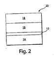
図2は、本発明の別の実施形態による半導体構造20を示している。半導体構造20は、当該構造が中間層15を含まないことを除いて、図1に示す構造と同様である。
図3は、本発明の別の実施形態による半導体構造22を示している。半導体構造22は、当該構造が中間層15または遷移層16を含まないことを除いて、図1に示す構造と同様である。
FIG. 2 illustrates a
FIG. 3 illustrates a
図4は、支えのない窒化ガリウム材料領域18を含む構造40を示している。支えのない窒化ガリウム材料領域は、窒化ガリウム材料領域下の基板及び層群(例えば、12,15,16)を除去することにより形成することができる。例えば、基板及び層群はエッチングプロセスにより除去することができる。この実施形態では、窒化ガリウム材料領域は、らせん転位密度が低いことを含む上に記載した特徴のいずれかを有することができる。詳細には、支えのない窒化ガリウム材料領域がほぼ一定の低いらせん転位密度を有すると有利である。構造40は更に処理することにより、例えば半導体素子を形成することができる。
FIG. 4 shows a
図4は窒化ガリウム材料領域18を示しているが、本明細書に記載する他のIII族窒化物材料のいずれかに処理を施して支えのない構造にすることもできることを理解されたい。
Although FIG. 4 shows the gallium
図1〜4に示す半導体構造は種々の半導体素子の基礎を構成することができる。適切な素子として、これらには制限されないが、トランジスタ(例えば、FET)だけでなく、LED及びレーザダイオードを含む発光素子を挙げることができる。これらの素子は活性領域を有し、活性領域は通常、少なくとも部分的に窒化ガリウム材料領域内に形成される。また、これらの素子は種々の他の機能層群及び/又はパターン群(例えば、電極群)を含む。 The semiconductor structures shown in FIGS. 1-4 can form the basis of various semiconductor elements. Suitable elements include, but are not limited to, light emitting elements including LEDs and laser diodes as well as transistors (eg, FETs). These devices have an active region, which is typically formed at least partially within the gallium nitride material region. These elements include various other functional layer groups and / or pattern groups (for example, electrode groups).
例えば、図5は本発明の一の実施形態によるFET素子30を示している。素子30はソース電極34と、ドレイン電極36と、そしてゲート電極38と、を含み、これらの電極は窒化ガリウム材料領域18(この窒化ガリウム材料領域は第1層18b及び第2層18aを含む)の上に形成される。素子は電極形成層40も含み、この層は図示のように、窒化ガリウム材料領域の表面を保護し、そして被覆するパッシベーション層である。ビア
42は電極形成層40内に形成され、電極形成層内には、ゲート電極の一部分が形成される。歪吸収層12は基板の上に直接形成され、そして中間層15は歪吸収層の上に直接形成される。或る実施形態では、中間層の組成には傾斜が付けられる。或る実施形態では、中間層は一定の組成(例えば、窒化アルミニウムまたは窒化アルミニウム合金)を有することができ、そして組成傾斜遷移層が歪吸収層の上に形成される。図示のように、窒化ガリウム材料領域は複数の窒化ガリウム材料層(18a,18b,18c)を含み、各層のらせん転位密度は低い。
For example, FIG. 5 illustrates a
或る実施形態では、層18bの窒化ガリウム材料は、層18aの窒化ガリウム材料のアルミニウム濃度よりも高いアルミニウム濃度を有することが好ましい。例えば、層18bの窒化ガリウム材料の(上に説明した窒化ガリウム材料のいずれかに関する)xの値は、層18aの窒化ガリウム材料のxの値よりも大きい、0.05〜1.0の間の値を有することができる、または層18aの窒化ガリウム材料のxの値よりも大きい、0.05〜0.5の間の値を有することができる。例えば、層18bはAl0.26Ga0.74Nにより形成することができ、層18aはGaNにより形成することができる。アルミニウム濃度のこの差によって、非常に高い導電率を持つ領域(例えば、2次元電子ガス領域)を層18bと層18aとの界面に形成することができる。図示の実施形態では、層18cはGaNにより形成することができる。
In certain embodiments, the gallium nitride material of
ここで、本明細書において詳細には説明されない構造及び素子を含む他の構造及び素子は、本発明の技術範囲に含まれることを理解されたい。他の構造は、異なる要素の中でもとりわけ、他の層及び/又はパターンを含むことができる。 Here, it should be understood that other structures and elements, including structures and elements not described in detail herein, are within the scope of the present invention. Other structures can include other layers and / or patterns, among other elements.
半導体構造10は公知の半導体処理技術を使用して形成することができる。歪吸収層が窒化シリコン系材料(例えば、アモルファスSiN)である実施形態では、歪吸収層は、シリコン基板の上側表面を上に記載したように窒化することにより形成することができる。窒化プロセスでは、窒素をシリコン基板の上側表面と反応させて窒化シリコン系の層を形成する。上側表面は、シリコン基板を高温の窒素ガス雰囲気中に曝すことにより窒化することができる。例えば、アンモニアを、シリコン基板が搬入されている反応室に導入することができる。反応室の温度は約1000℃〜1100℃の範囲とすることができ、圧力は約20torr〜約40torrの範囲とすることができる(或る場合においては、約30torr)。窒素とシリコン基板との反応は、所望の膜厚を有する層が形成されるように選択される反応時間に渡って行なわれる。
The
ここで、他のプロセスを使用して窒化シリコン系の歪吸収層を形成することができ、他のプロセスとして、別々の窒素ソース及びシリコンソースを使用するプロセス(例えばCVDプロセス)を挙げることができることを理解されたい。また、歪吸収層を別のタイプの材料(窒化シリコン系材料以外の材料)により形成する場合、この技術分野で公知の他の堆積プロセスが使用される。 Here, a silicon nitride-based strain absorption layer can be formed using another process, and the process using separate nitrogen source and silicon source (for example, CVD process) can be cited as another process. I want you to understand. Also, if the strain absorbing layer is formed from another type of material (a material other than a silicon nitride based material), other deposition processes known in the art are used.
或る実施形態では、歪吸収層は構造の中間層(及び、或る場合においては、中間層に続いて形成される層)にin−situで形成することができる。すなわち、歪吸収層は同じ堆積工程の間に中間層(及び、或る場合においては、中間層に続いて形成される層)として形成することができる。窒化シリコン系材料から成る歪吸収層を、窒素含有ガス(例えばアンモニア)を反応室に上述のように導入することにより成長させるプロセスでは、第2のソースガスを、窒素含有ガス導入後の或る選択された時間だけ遅れて反応室に導入することができる。第2のソースガスが窒素含有ガスと反応して中間層を形成することにより、歪吸収層の成長が終了する。例えば、中間層が窒化アルミニウムにより形成される場合、アルミニウム含有ガス(例えば、トリメチルアルミニウム)を反応室に、窒素含有ガス(例えばアンモニア)導入後の或る選択された時間だけ遅らせた時点で導入する。遅
延時間は、歪吸収層が所望の膜厚を有するようになるまで成長するように選択される。第2のソースガス(例えば、アルミニウム含有ガス)と窒素含有ガスとの間の反応は、中間層を形成するために十分な時間を費やして行なわれる。中間層が単結晶構造を有する場合、反応条件が適切に選択される。例えば、反応温度は700℃よりも高く、約1000℃〜約1100℃の範囲とすることができる。或る場合においては、これよりも低い成長温度を使用することができ、この温度として約500℃〜約600℃の範囲を挙げることができる。
In some embodiments, the strain-absorbing layer can be formed in-situ on the intermediate layer of the structure (and in some cases, a layer formed subsequent to the intermediate layer). That is, the strain absorbing layer can be formed as an intermediate layer (and in some cases, a layer formed subsequent to the intermediate layer) during the same deposition process. In a process of growing a strain absorbing layer made of a silicon nitride-based material by introducing a nitrogen-containing gas (for example, ammonia) into the reaction chamber as described above, the second source gas is a certain amount after the introduction of the nitrogen-containing gas. It can be introduced into the reaction chamber with a delay of a selected time. The second source gas reacts with the nitrogen-containing gas to form the intermediate layer, thereby completing the growth of the strain absorbing layer. For example, when the intermediate layer is formed of aluminum nitride, an aluminum-containing gas (eg, trimethylaluminum) is introduced into the reaction chamber at a time that is delayed by a selected time after the introduction of the nitrogen-containing gas (eg, ammonia). . The delay time is selected to grow until the strain absorbing layer has the desired film thickness. The reaction between the second source gas (eg, aluminum-containing gas) and the nitrogen-containing gas is performed with sufficient time to form the intermediate layer. When the intermediate layer has a single crystal structure, the reaction conditions are appropriately selected. For example, the reaction temperature can be higher than 700 ° C. and can range from about 1000 ° C. to about 1100 ° C. In some cases, lower growth temperatures can be used, and this temperature can range from about 500 ° C to about 600 ° C.
ここで、歪吸収層は中間層及びそれに続く層とは別のプロセスにより形成することができることも理解されたい。例えば、歪吸収層は基板の上に第1プロセスで形成することができる。次に、その後の時点で、中間層を歪吸収層の上に第2プロセスで形成することができる。 It should also be understood that the strain absorbing layer can be formed by a process different from the intermediate layer and subsequent layers. For example, the strain absorbing layer can be formed on the substrate by a first process. Then, at a later time, the intermediate layer can be formed on the strain absorbing layer in a second process.
上に説明したプロセスでは、中間層は垂直成長プロセスで成長させる。すなわち、中間層は歪吸収層に対して垂直方向に(すなわち、図1のy軸に沿って)成長させる。ミスフィット転位密度が低い(これによりらせん転位密度を低くすることができる)歪吸収層を垂直に成長させる機能は、垂直成長プロセスよりも複雑な横方向成長プロセスよりも有利となり得る。 In the process described above, the intermediate layer is grown in a vertical growth process. That is, the intermediate layer is grown in a direction perpendicular to the strain absorbing layer (that is, along the y-axis in FIG. 1). The ability to grow strain absorbing layers vertically with low misfit dislocation density (which can reduce screw dislocation density) can be advantageous over complex lateral growth processes over vertical growth processes.
遷移層16及び窒化ガリウム材料領域18も、中間層及び歪吸収層と同じ堆積工程において成長させることができる。このようなプロセスでは、適切なソースガスが反応室に適切な時間に導入される。
一の好適な方法によれば、遷移層及び窒化ガリウム材料領域(及び、設ける場合の中間層)は有機金属化学気相成長(MOCVD)プロセスを使用して成長させる。ここで、この技術分野で公知の他の適切な方法を使用して遷移層及び窒化ガリウム材料領域を堆積させることもでき、この方法として、分子線エピタキシー法(BME)、ハライド気相エピタキシー法(HVPE)などを挙げることができることを理解されたい。 According to one preferred method, the transition layer and the gallium nitride material region (and the intermediate layer, if provided) are grown using a metal organic chemical vapor deposition (MOCVD) process. Here, the transition layer and the gallium nitride material region can also be deposited using other suitable methods known in the art, including molecular beam epitaxy (BME), halide vapor phase epitaxy ( (HVPE) and the like.
一般的に、MOCVDプロセスでは、異なるソースガスを利用環境(例えば、プロセスシステム)に導入し、そしてガスの間の反応を促進する条件を設定して層を形成する。反応は所望厚さの層が形成されるまで行なわれる。層の組成は以下に更に説明するように、ガス組成、ガス濃度、及び反応条件(例えば、温度及び圧力)を含む幾つかの要素によって制御することができる。 In general, in a MOCVD process, different source gases are introduced into a use environment (eg, a process system), and conditions are set to promote reactions between the gases to form layers. The reaction is conducted until a layer of the desired thickness is formed. The composition of the layer can be controlled by several factors including gas composition, gas concentration, and reaction conditions (eg, temperature and pressure), as further described below.
遷移層及び窒化ガリウム材料領域をMOCVD成長させるための適切なソースガスの例として、アルミニウム含有ガスとしてのトリメチルアルミニウム(TMA)またはトリエチルアルミニウム(TEA)、インジウム含有ガスとしてのトリメチルインジウム(TMI)またはトリエチルインジウム(TEI)、ガリウム含有ガスとしてのトリメチルガリウム(TMG)またはトリエチルガリウム(TEG)、そして窒素含有ガスとしてのアンモニア(NH3)を挙げることができる。使用する特定のソースガスは、層の所望の組成によって変わる。例えば、アルミニウム含有ガス(例えば、TMAまたはTEA)、ガリウム含有ガス(TMGまたはTEG)、及び窒素含有ガスを使用してAlxGa1−xN組成を有する膜を堆積させる。 Examples of suitable source gases for MOCVD growth of the transition layer and gallium nitride material region include trimethylaluminum (TMA) or triethylaluminum (TEA) as an aluminum-containing gas, trimethylindium (TMI) or triethyl as an indium-containing gas Indium (TEI), trimethylgallium (TMG) or triethylgallium (TEG) as a gallium-containing gas, and ammonia (NH 3 ) as a nitrogen-containing gas can be mentioned. The particular source gas used will depend on the desired composition of the layer. For example, an aluminum-containing gas (eg, TMA or TEA), a gallium-containing gas (TMG or TEG), and a nitrogen-containing gas are used to deposit a film having an Al x Ga 1-x N composition.
ソースガスの流量、ソースガスの比、及びソースガスの絶対濃度を制御して所望の組成を有する遷移層及び窒化ガリウム材料領域を形成することができる。AlxGa1−xN層を成長させる場合、通常のTMA流量は約5マイクロモル/分〜約50マイクロモル/分であり、当該流量は或る場合においては約20マイクロモル/分が好ましく、通常のTMG流量は約5マイクロモル/分〜約250マイクロモル/分であり、当該流量は或る場
合においては約115マイクロモル/分が好ましく、そしてアンモニア流量は通常、約3slpm〜約10slpmである。反応温度は通常、約900℃〜約1200℃であり、そしてプロセス圧力は約1Torr〜約760Torrである。ここで、プロセス条件、特に流量はプロセスシステム構成によって大きく変わることを理解されたい。通常、スループットが小さいシステムでは、スループットの大きいシステムよりも流量を小さくする必要がある。
The transition layer and the gallium nitride material region having a desired composition can be formed by controlling the flow rate of the source gas, the ratio of the source gas, and the absolute concentration of the source gas. When growing an Al x Ga 1-x N layer, a typical TMA flow rate is about 5 micromole / minute to about 50 micromole / minute, and in some cases, the flow rate is preferably about 20 micromole / minute. A typical TMG flow rate is from about 5 micromole / minute to about 250 micromole / minute, and the flow rate is preferably about 115 micromole / minute in some cases, and the ammonia flow rate is typically from about 3 slpm to about 10 slpm. It is. The reaction temperature is typically about 900 ° C. to about 1200 ° C., and the process pressure is about 1 Torr to about 760 Torr. Here, it should be understood that process conditions, particularly flow rates, vary greatly with process system configuration. Usually, in a system with low throughput, the flow rate needs to be smaller than in a system with high throughput.
組成傾斜を付けた遷移層を形成する場合、プロセスパラメータを適切に調整して組成傾斜を制御する必要がある。組成には、プロセス条件を変えて特定の組成が選択的に成長するようにすることにより傾斜を付けることができる。例えば、遷移層に取り込むガリウムを増やすことによりガリウム濃度を高くするために、ガリウム含有ガス(例えば、TMGまたはTEG)の流量及び/又は濃度を大きくすることができる。同様にして、遷移層に取り込むアルミニウムを増やすことによりアルミニウム濃度を高くするために、アルミニウム含有ガス(例えば、TMAまたはTEA)の流量及び/又は濃度を大きくすることができる。ソースガスの流量及び/又は濃度を大きくする(または小さくする)方法によって、組成に傾斜を付ける方法を制御することができる。他の実施形態では、温度及び/又は圧力を調整して特定の化合物を選択的に成長させる。ガリウムを選択的に遷移層に取り込むための成長温度及び圧力は、アルミニウムを選択的に遷移層に取り込むための成長温度及び圧力とは異なる。従って、組成には、温度及び圧力を適切に調整することにより傾斜を付けることができる。 When forming a transition layer with a composition gradient, it is necessary to control the composition gradient by appropriately adjusting process parameters. The composition can be graded by changing the process conditions to selectively grow a particular composition. For example, the flow rate and / or concentration of a gallium-containing gas (eg, TMG or TEG) can be increased to increase the gallium concentration by increasing the gallium incorporated into the transition layer. Similarly, the flow rate and / or concentration of an aluminum-containing gas (eg, TMA or TEA) can be increased to increase the aluminum concentration by increasing the aluminum incorporated into the transition layer. The method of grading the composition can be controlled by increasing (or decreasing) the flow rate and / or concentration of the source gas. In other embodiments, the temperature and / or pressure is adjusted to selectively grow certain compounds. The growth temperature and pressure for selectively incorporating gallium into the transition layer are different from the growth temperature and pressure for selectively incorporating aluminum into the transition layer. Therefore, the composition can be graded by adjusting the temperature and pressure appropriately.
しかしながら、一定の組成を有する遷移層または窒化ガリウム材料領域(或いは、中間層)を堆積させる場合、プロセスパラメータを一定に維持して一定の組成を有する層が形成されるようにする。窒化ガリウム材料領域が、それぞれ異なる組成を有する一つよりも多くの窒化ガリウム材料層を含む場合、プロセスパラメータを適切な時点で変更して、形成される層の組成を変更することができる。 However, when depositing a transition layer or gallium nitride material region (or intermediate layer) having a constant composition, the process parameters are kept constant so that a layer having a constant composition is formed. If the gallium nitride material region includes more than one gallium nitride material layer, each having a different composition, the process parameters can be changed at the appropriate time to change the composition of the formed layer.
ここで、基板上の層群/領域群(すなわち、歪吸収層、中間層、遷移層、及び窒化ガリウム材料領域)の全てを同じプロセスにより成長させることができることを理解されたい。或いは、それぞれの層群/領域群は別々に成長させることができる。 Here, it should be understood that all of the layers / regions (ie, strain absorbing layer, intermediate layer, transition layer, and gallium nitride material region) on the substrate can be grown by the same process. Alternatively, each layer / region group can be grown separately.
説明したプロセスでは、層群/領域群(すなわち、歪吸収層、中間層、遷移層、及び窒化ガリウム材料領域)を垂直成長プロセスにより成長させる。すなわち、これらの層群/領域群を下地の層群/領域群(基板を含む)に対して垂直方向に成長させる。らせん転位密度が低い窒化ガリウム材料領域を含む層群/領域群を垂直に成長させる機能は、垂直成長プロセスよりも複雑な横方向成長プロセスよりも有利となり得る。 In the process described, layers / regions (ie, strain absorbing layers, interlayers, transition layers, and gallium nitride material regions) are grown by a vertical growth process. That is, these layer groups / region groups are grown in a direction perpendicular to the underlying layer group / region group (including the substrate). The ability to vertically grow layers / regions containing gallium nitride material regions with low screw dislocation density can be advantageous over more complex lateral growth processes than vertical growth processes.
しかしながら、本発明の他の実施形態(図示せず)では、窒化ガリウム材料領域18の少なくとも一部分を、エピタキシャル横方向成長(LEO)法を使用して成長させることが可能であり、このエピタキシャル横方向成長法では、下地の窒化ガリウム層を、マスク(非晶質の膜)に設けた細い線状の窓を通して成長させ、次にマスクの上を横方向に成長させて窒化ガリウム材料領域を形成するが、この方法は、例えば米国特許第6,051,849号に記載されている。
However, in other embodiments (not shown) of the present invention, at least a portion of the gallium
本発明の他の実施形態(図示せず)では、窒化ガリウム材料領域18を、PENDEO成長法を使用して成長させることが可能であり、このPENDEO成長法では、隣接するサイドウォールからの成長が融合するまで窒化ガリウム材料柱状構造のサイドウォールをトレンチ内に成長させて窒化ガリウム材料領域を形成するが、これについては、例えば米国特許第6,265,289号に記載されている。これらの実施形態では、例えば歪吸収層12(及び、或る場合においては、層15,16)を横方向成長の前にサイドウォール
に堆積させることができ、これにより横方向成長によるIII族窒化物材料層群/領域群(例えば、窒化ガリウム材料領域)におけるらせん転位密度を小さくすることができる。
In other embodiments of the present invention (not shown), the gallium
本出願と同じ譲受人が保有する同時係属中の、2003年12月17日出願の「電極形成層を含む窒化ガリウム材料素子、及び同素子を形成する方法」と題する文献であって、この文献を本明細書において参照することにより、この文献の内容が本発明の開示に含まれることになる米国特許出願番号10/740,376は、図5の実施形態に示す他の層及びパターンを成長させるために使用される方法について更に記載している。 A document entitled "Gallium nitride material element including electrode forming layer and method for forming the same" filed on December 17, 2003, owned by the same assignee as the present application. U.S. Patent Application No. 10 / 740,376, the contents of which are included in the disclosure of this invention, is a growth of other layers and patterns shown in the embodiment of FIG. The method used to achieve this is further described.
ここで、この技術分野の当業者には公知の他のプロセスを使用して本発明の構造及び素子を形成することができることも理解されたい。
次の実施例は本発明を例示するためのものであり、本発明を制限するものではない。
(実施例1)
この実施例は、本発明の一の実施形態による、らせん転位密度が低いIII族窒化物材料層群/領域群を含む構造を形成する様子を示す。
It should also be understood that other processes known to those skilled in the art can be used to form the structures and elements of the present invention.
The following examples are intended to illustrate the invention and are not intended to limit the invention.
(Example 1)
This example illustrates the formation of a structure including a group III / nitride material layer / region group with low screw dislocation density according to one embodiment of the present invention.
100mmのシリコン基板を反応室に搬入した。アンモニアガスを反応室に窒素含有ガスとして導入した。温度を1030℃に維持し、かつ圧力を約30torrに維持した。アモルファス窒化シリコン(SiN)から成る歪吸収層を形成した。 A 100 mm silicon substrate was carried into the reaction chamber. Ammonia gas was introduced into the reaction chamber as a nitrogen-containing gas. The temperature was maintained at 1030 ° C. and the pressure was maintained at about 30 torr. A strain absorbing layer made of amorphous silicon nitride (SiN) was formed.
アンモニアを導入した後、約6秒経過した時点で、TMAを反応室にアルミニウム含有ガスとして導入した。温度及び圧力はそれぞれ1030℃及び約30torrに維持した。成長は約60分間行なった。窒化アルミニウム(AlN)を形成した。 After about 6 seconds had passed after introducing ammonia, TMA was introduced into the reaction chamber as an aluminum-containing gas. The temperature and pressure were maintained at 1030 ° C. and about 30 torr, respectively. Growth was carried out for about 60 minutes. Aluminum nitride (AlN) was formed.
約60分経過した時点で、TMGを反応室に導入した。成長は約40分間行なった。窒化アルミニウムガリウム層(Al0.6Ga0.4N)を形成した。
約40分経過した時点で、反応室に導入しているTMGの濃度を高くし、そして反応室に導入しているTMAの濃度を低くした。成長は約20分間行なった。窒化アルミニウムガリウム層(Al0.3Ga0.7N)を形成した。
At about 60 minutes, TMG was introduced into the reaction chamber. Growth was carried out for about 40 minutes. An aluminum gallium nitride layer (Al 0.6 Ga 0.4 N) was formed.
When about 40 minutes passed, the concentration of TMG introduced into the reaction chamber was increased, and the concentration of TMA introduced into the reaction chamber was decreased. Growth was carried out for about 20 minutes. An aluminum gallium nitride layer (Al 0.3 Ga 0.7 N) was formed.
約20分経過した時点で、TMAの供給を止め、そしてTMGのみを反応室に導入した。窒化ガリウム(GaN)層を形成した。成長は30分間行なった。
TMAの供給を再開し、そしてTMA及びTMGを反応室に導入して薄い窒化アルミニウムガリウム層を成長させた。
At about 20 minutes, the supply of TMA was stopped and only TMG was introduced into the reaction chamber. A gallium nitride (GaN) layer was formed. Growth was for 30 minutes.
The TMA supply was resumed and TMA and TMG were introduced into the reaction chamber to grow a thin aluminum gallium nitride layer.
図6はSTEM(scanning transmission electron microscope:走査透過電子顕微鏡)画像のコピーであり、この画像は窒化シリコン歪吸収層が窒化アルミニウム層とシリコン基板との間に形成されている様子を示している。 FIG. 6 is a copy of a STEM (Scanning Transmission Electron Microscope) image, which shows a silicon nitride strain absorbing layer formed between the aluminum nitride layer and the silicon substrate.
gベクトルの解析を行ない、被覆III族窒化物材料層群/領域群のらせん転位密度を従来のTEM法を使用して求めた。図7A〜8Bは、同じ構造の垂直方向断面を撮影したTEM画像のコピーである。参照記号については、「*」は画像の同じ空間位置を指している。 The g vector was analyzed, and the screw dislocation density of the coated group III nitride material layer group / region group was determined using a conventional TEM method. 7A-8B are copies of TEM images taken of vertical sections of the same structure. For reference symbols, “ * ” refers to the same spatial location of the image.
図7Aは基板表面に直交するgベクトル(g=(00001))を含む画像である。図7Bは基板表面に平行なgベクトル(g=(1−100))を含む画像である。
図8A及び8Bはそれぞれ、図7A及び7Bのコピーであり、この場合、転位が窒化物材料領域に含まれ、そして遷移層(Al0.3Ga0.7N)の第1部分が破線によって
目立つようにしてある。ここで、AlGaN遷移層の第2部分、及びAlN層は同様の転位密度を示すが、説明を分かり易くするために、破線で個々に示すということは行なっていないことに留意されたい。
FIG. 7A is an image including a g vector (g = (00001)) orthogonal to the substrate surface. FIG. 7B is an image including a g vector (g = (1-100)) parallel to the substrate surface.
8A and 8B are copies of FIGS. 7A and 7B, respectively, where dislocations are included in the nitride material region and the first portion of the transition layer (Al 0.3 Ga 0.7 N) is represented by a dashed line. It stands out. Here, it should be noted that the second portion of the AlGaN transition layer and the AlN layer show the same dislocation density, but are not shown individually by broken lines for the sake of easy understanding.
図示のように、図7A及び図8Aに観察される転位の全てを図7B及び図8Bにも観察することができる。この1対1の対応が、これらの転位の全てが刃状転位または混合転位(刃状転位成分を含む)であることを示している。従って、らせん転位はTEM画像には全く観察されなかった。 As shown, all of the dislocations observed in FIGS. 7A and 8A can also be observed in FIGS. 7B and 8B. This one-to-one correspondence indicates that all of these dislocations are edge dislocations or mixed dislocations (including edge dislocation components). Therefore, no screw dislocation was observed in the TEM image.
また、図7A及び図8Aには観察されない多数の転位が図7B及び図8Bに観察される。これは、これらの転位が刃状転位または混合転位であることも示唆している。
この実施例によって、らせん転位密度が非常に低いIII族窒化物材料層群/領域群を形成する方法を求めることができる。らせん転位はTEM画像からは全く検出することができなかった。
Also, a number of dislocations not observed in FIGS. 7A and 8A are observed in FIGS. 7B and 8B. This also suggests that these dislocations are edge dislocations or mixed dislocations.
According to this embodiment, a method of forming a group III / nitride material layer group / region group having a very low screw dislocation density can be obtained. No screw dislocations could be detected from the TEM image.
上述のようにして本発明の少なくとも一つの実施形態の幾つかの態様について説明してきたが、この技術分野の当業者であれば、種々の変更、変形、及び改良を容易に本発明に加え得ることが理解できるであろう。このような変更、変形、及び改良は本開示の一部分となるものであり、かつ本発明の技術思想及び技術範囲に含まれるものである。従って、これまでの記述及び図はほんの一例として提示される。 While several aspects of at least one embodiment of the present invention have been described above, various changes, modifications, and improvements can be readily added to the present invention by those skilled in the art. You will understand that. Such alterations, modifications, and improvements are part of this disclosure and are intended to be within the spirit and scope of the invention. Accordingly, the foregoing description and figures are presented by way of example only.
Claims (20)
前記シリコン基板の上側表面の窒化によって設けられた、シリコン基板の上側表面のアモルファス窒化シリコンの歪吸収層と、
アモルファス窒化シリコンの前記歪吸収層の上に形成されたIII族窒化物材料領域であって、らせん転位密度が該III族窒化物材料領域全体に渡って108/cm2未満であり、かつ、刃状転位密度が108/cm2よりも高いIII族窒化物材料領域とを備える、半導体構造。 A silicon substrate;
Provided by nitriding the upper surface of the silicon substrate, an amorphous silicon nitride strain absorbing layer on the upper surface of the silicon substrate;
A group III nitride material region formed on the strain absorbing layer of amorphous silicon nitride, the screw dislocation density being less than 10 8 / cm 2 throughout the group III nitride material region; and A semiconductor structure comprising a group III nitride material region having an edge dislocation density higher than 10 8 / cm 2 .
前記シリコン基板の上側表面の窒化によって設けられた、シリコン基板の上側表面のアモルファス窒化シリコンの歪吸収層と、
アモルファス窒化シリコンの前記歪吸収層の上に形成されたIII族窒化物材料領域とを備え、前記III族窒化物材料領域は少なくとも100ミクロン×100ミクロンの寸法、104/cm2未満のらせん転位密度、かつ108/cm2よりも高い刃状転位密度を有する領域を含む、半導体構造。 A silicon substrate;
Provided by nitriding the upper surface of the silicon substrate, an amorphous silicon nitride strain absorbing layer on the upper surface of the silicon substrate;
A group III nitride material region formed on the strain absorbing layer of amorphous silicon nitride, the group III nitride material region having dimensions of at least 100 microns x 100 microns and a screw dislocation of less than 10 4 / cm 2 A semiconductor structure comprising a region having a density and an edge dislocation density higher than 10 8 / cm 2 .
前記シリコン基板の上側表面の窒化によって設けられた、シリコン基板の上側表面のアモルファス窒化シリコンの歪吸収層と、
上側表面の上に形成され、かつ前記歪吸収層とは異なる組成を有するIII族窒化物材料領域と、を備え、上側表面の100ナノメートル以内のIII族窒化物材料領域の断面領域は、108/cm2未満のらせん転位密度、及び108/cm2よりも高い刃状転位密度を有する、半導体構造。 A silicon substrate;
Provided by nitriding the upper surface of the silicon substrate, an amorphous silicon nitride strain absorbing layer on the upper surface of the silicon substrate;
A group III nitride material region formed on the upper surface and having a composition different from that of the strain absorbing layer, and the cross-sectional region of the group III nitride material region within 100 nanometers of the upper surface is 10 A semiconductor structure having a screw dislocation density of less than 8 8 / cm 2 and an edge dislocation density higher than 10 8 / cm 2 .
アモルファス窒化シリコンの前記歪吸収層の上に形成されたIII族窒化物材料領域を備え、前記III族窒化物材料領域は刃状転位密度と、10 8 /cm 2 未満のらせん転位密度とを有し、前記刃状転位密度はらせん転位密度の少なくとも100倍の大きさである、半導体構造。 A strain absorbing layer of amorphous silicon nitride formed from the upper substrate of the silicon substrate;
Comprising a III-nitride material region formed on the strain-absorbing layer of amorphous silicon nitride, organic the III nitride material region and the edge dislocation density of less than 10 8 / cm 2 and a screw dislocation density and the edge dislocation density is at least 100 times as large as the screw dislocation density, the semiconductor structure.
前記シリコン基板の上側表面の窒化によって設けられた、シリコン基板の上側表面のアモルファス窒化シリコンの歪吸収層であって、100オングストローム未満の膜厚を有し、かつ前記シリコン基板の上側表面の全体を覆う、歪吸収層と、
アモルファス窒化シリコンの前記歪吸収層の上に形成され、かつ108/cm2未満のらせん転位密度、及び108/cm2よりも高い刃状転位密度を有するIII族窒化物材料領域と、を備える半導体構造。 A silicon substrate;
An amorphous silicon nitride strain-absorbing layer provided on the upper surface of the silicon substrate by nitriding the upper surface of the silicon substrate, having a film thickness of less than 100 angstroms, and covering the entire upper surface of the silicon substrate Covering the strain absorbing layer,
Formed on the strain-absorbing layer of amorphous silicon nitride, and the screw dislocation density of less than 10 8 / cm 2, and the III-nitride material region having edge dislocation density higher than 10 8 / cm 2, the A semiconductor structure comprising.
シリコン基板を設ける工程と、
前記シリコン基板の上側表面のアモルファス窒化シリコンの歪吸収層を形成するために
前記シリコン基板の上側表面を窒化する工程と、
アモルファス窒化シリコンの前記歪吸収層の上方に窒化ガリウム材料領域を形成する工程とを備え、前記窒化ガリウム材料領域は、108/cm2未満のらせん転位密度、及び108/cm2よりも高い刃状転位密度を有する、方法。 A method of forming a semiconductor structure comprising:
Providing a silicon substrate;
Nitriding the upper surface of the silicon substrate to form an amorphous silicon nitride strain absorbing layer on the upper surface of the silicon substrate;
And forming an upper gallium nitride material region of amorphous the strain-absorbing layer of silicon nitride, the gallium nitride material region is higher than 10 8 / cm 2 less than the density of screw dislocations, and 10 8 / cm 2 A method having an edge dislocation density.
Applications Claiming Priority (3)
| Application Number | Priority Date | Filing Date | Title |
|---|---|---|---|
| US10/886,506 US7687827B2 (en) | 2004-07-07 | 2004-07-07 | III-nitride materials including low dislocation densities and methods associated with the same |
| US10/886,506 | 2004-07-07 | ||
| PCT/US2005/023934 WO2006014472A1 (en) | 2004-07-07 | 2005-07-06 | Iii-nitride materials including low dislocation densities and methods associated with the same |
Publications (3)
| Publication Number | Publication Date |
|---|---|
| JP2008505834A JP2008505834A (en) | 2008-02-28 |
| JP2008505834A5 JP2008505834A5 (en) | 2008-08-14 |
| JP5705399B2 true JP5705399B2 (en) | 2015-04-22 |
Family
ID=34973093
Family Applications (1)
| Application Number | Title | Priority Date | Filing Date |
|---|---|---|---|
| JP2007520461A Expired - Fee Related JP5705399B2 (en) | 2004-07-07 | 2005-07-06 | Group III nitride materials with low dislocation density and methods related to the materials |
Country Status (4)
| Country | Link |
|---|---|
| US (2) | US7687827B2 (en) |
| EP (1) | EP1778897B1 (en) |
| JP (1) | JP5705399B2 (en) |
| WO (1) | WO2006014472A1 (en) |
Families Citing this family (50)
| Publication number | Priority date | Publication date | Assignee | Title |
|---|---|---|---|---|
| US7071498B2 (en) * | 2003-12-17 | 2006-07-04 | Nitronex Corporation | Gallium nitride material devices including an electrode-defining layer and methods of forming the same |
| US7339205B2 (en) * | 2004-06-28 | 2008-03-04 | Nitronex Corporation | Gallium nitride materials and methods associated with the same |
| US7687827B2 (en) * | 2004-07-07 | 2010-03-30 | Nitronex Corporation | III-nitride materials including low dislocation densities and methods associated with the same |
| JP2008519441A (en) * | 2004-10-28 | 2008-06-05 | ニトロネックス コーポレイション | Monolithic microwave integrated circuit using gallium nitride material |
| FI20045482A0 (en) * | 2004-12-14 | 2004-12-14 | Optogan Oy | A semiconductor substrate having a lower dislocation density, and a process for its preparation |
| JP5135686B2 (en) * | 2005-03-23 | 2013-02-06 | 住友電気工業株式会社 | Group III nitride semiconductor device |
| US7365374B2 (en) * | 2005-05-03 | 2008-04-29 | Nitronex Corporation | Gallium nitride material structures including substrates and methods associated with the same |
| US8946674B2 (en) * | 2005-08-31 | 2015-02-03 | University Of Florida Research Foundation, Inc. | Group III-nitrides on Si substrates using a nanostructured interlayer |
| WO2007041710A2 (en) * | 2005-10-04 | 2007-04-12 | Nitronex Corporation | Gallium nitride material transistors and methods for wideband applications |
| US7566913B2 (en) | 2005-12-02 | 2009-07-28 | Nitronex Corporation | Gallium nitride material devices including conductive regions and methods associated with the same |
| EP1969635B1 (en) | 2005-12-02 | 2017-07-19 | Infineon Technologies Americas Corp. | Gallium nitride material devices and associated methods |
| US7777217B2 (en) | 2005-12-12 | 2010-08-17 | Kyma Technologies, Inc. | Inclusion-free uniform semi-insulating group III nitride substrate and methods for making same |
| JP2007161536A (en) * | 2005-12-14 | 2007-06-28 | Sumitomo Electric Ind Ltd | AlxGayIn1-x-yN CRYSTAL SUBSTRATE, SEMICONDUCTOR DEVICE AND ITS MANUFACTURING METHOD |
| US20100269819A1 (en) * | 2006-08-14 | 2010-10-28 | Sievers Robert E | Human Powered Dry Powder Inhaler and Dry Powder Inhaler Compositions |
| JP4282708B2 (en) * | 2006-10-20 | 2009-06-24 | 株式会社東芝 | Nitride semiconductor devices |
| US7951693B2 (en) * | 2006-12-22 | 2011-05-31 | Philips Lumileds Lighting Company, Llc | III-nitride light emitting devices grown on templates to reduce strain |
| JP5383974B2 (en) * | 2006-12-27 | 2014-01-08 | 住友電工デバイス・イノベーション株式会社 | Semiconductor substrate and semiconductor device |
| KR101330251B1 (en) * | 2007-03-06 | 2013-11-15 | 서울바이오시스 주식회사 | Method of forming nitride semiconductor layer on a patterned substrate and light emitting diode having the layer |
| US8362503B2 (en) * | 2007-03-09 | 2013-01-29 | Cree, Inc. | Thick nitride semiconductor structures with interlayer structures |
| US7825432B2 (en) | 2007-03-09 | 2010-11-02 | Cree, Inc. | Nitride semiconductor structures with interlayer structures |
| US7745848B1 (en) | 2007-08-15 | 2010-06-29 | Nitronex Corporation | Gallium nitride material devices and thermal designs thereof |
| US8026581B2 (en) * | 2008-02-05 | 2011-09-27 | International Rectifier Corporation | Gallium nitride material devices including diamond regions and methods associated with the same |
| US20090218589A1 (en) * | 2008-03-01 | 2009-09-03 | Goldeneye, Inc. | Semiconductor die with reduced thermal boundary resistance |
| US8343824B2 (en) * | 2008-04-29 | 2013-01-01 | International Rectifier Corporation | Gallium nitride material processing and related device structures |
| US8703623B2 (en) * | 2009-06-01 | 2014-04-22 | Massachusetts Institute Of Technology | Fabrication technique for gallium nitride substrates |
| JP2011023534A (en) | 2009-07-15 | 2011-02-03 | Sumitomo Electric Ind Ltd | Nitride-based semiconductor light emitting element |
| DE102009047881B4 (en) * | 2009-09-30 | 2022-03-03 | OSRAM Opto Semiconductors Gesellschaft mit beschränkter Haftung | Process for producing an epitaxially produced layer structure |
| EP2498293B1 (en) * | 2009-11-06 | 2018-08-01 | NGK Insulators, Ltd. | Epitaxial substrate for semiconductor element and method for producing epitaxial substrate for semiconductor element |
| US8648387B2 (en) * | 2009-12-30 | 2014-02-11 | Industrial Technology Research Institute | Nitride semiconductor template and method of manufacturing the same |
| CN102823088A (en) | 2010-04-05 | 2012-12-12 | 加利福尼亚大学董事会 | Aluminum gallium nitride barriers and separate confinement heterostructure (sch) layers for semipolar plane iii-nitride semiconductor-based light emitting diodes and laser diodes |
| GB2485418B (en) | 2010-11-15 | 2014-10-01 | Dandan Zhu | Semiconductor materials |
| JP5136867B2 (en) | 2011-02-03 | 2013-02-06 | 次世代パワーデバイス技術研究組合 | Semiconductor substrate, semiconductor device, and semiconductor substrate manufacturing method |
| US20130026480A1 (en) * | 2011-07-25 | 2013-01-31 | Bridgelux, Inc. | Nucleation of Aluminum Nitride on a Silicon Substrate Using an Ammonia Preflow |
| WO2013038980A1 (en) * | 2011-09-15 | 2013-03-21 | シャープ株式会社 | Substrate having buffer layer structure for growing nitride semiconductor layer |
| JP5139567B1 (en) * | 2011-09-22 | 2013-02-06 | シャープ株式会社 | Substrate having a buffer layer structure for growing a nitride semiconductor layer |
| JP5903818B2 (en) * | 2011-09-26 | 2016-04-13 | 富士通株式会社 | Compound semiconductor device and manufacturing method thereof |
| US20130082274A1 (en) | 2011-09-29 | 2013-04-04 | Bridgelux, Inc. | Light emitting devices having dislocation density maintaining buffer layers |
| US8664679B2 (en) | 2011-09-29 | 2014-03-04 | Toshiba Techno Center Inc. | Light emitting devices having light coupling layers with recessed electrodes |
| US8853668B2 (en) | 2011-09-29 | 2014-10-07 | Kabushiki Kaisha Toshiba | Light emitting regions for use with light emitting devices |
| US9012921B2 (en) | 2011-09-29 | 2015-04-21 | Kabushiki Kaisha Toshiba | Light emitting devices having light coupling layers |
| US8698163B2 (en) | 2011-09-29 | 2014-04-15 | Toshiba Techno Center Inc. | P-type doping layers for use with light emitting devices |
| US9178114B2 (en) | 2011-09-29 | 2015-11-03 | Manutius Ip, Inc. | P-type doping layers for use with light emitting devices |
| JP5705179B2 (en) * | 2012-08-15 | 2015-04-22 | 株式会社東芝 | Nitride semiconductor wafer, nitride semiconductor device, and method for growing nitride semiconductor crystal |
| JP5881560B2 (en) * | 2012-08-30 | 2016-03-09 | 株式会社東芝 | Semiconductor light emitting device and manufacturing method thereof |
| KR101590309B1 (en) * | 2013-07-22 | 2016-01-29 | 엔지케이 인슐레이터 엘티디 | Composite substrate, method for fabricating same, function element, and seed crystal substrate |
| KR20150103800A (en) * | 2014-03-04 | 2015-09-14 | 전북대학교산학협력단 | Heterostructure field effect transistor having high efficiency and method of preparing the same |
| FR3031834B1 (en) * | 2015-01-21 | 2018-10-05 | Centre National De La Recherche Scientifique (Cnrs) | FABRICATION OF A SEMICONDUCTOR SUPPORT BASED ON ELEMENT III NITRIDE |
| FR3031833B1 (en) * | 2015-01-21 | 2018-10-05 | Centre National De La Recherche Scientifique (Cnrs) | PROCESS FOR MANUFACTURING A PASSIVE ELEMENTS III-BASED NITRIDE SEMICONDUCTOR STRUCTURE AND SUCH A STRUCTURE |
| JP6195125B2 (en) * | 2015-02-25 | 2017-09-13 | 株式会社タムラ製作所 | Nitride semiconductor template and manufacturing method thereof |
| GB2584150B (en) | 2019-05-24 | 2021-05-19 | Plessey Semiconductors Ltd | LED precursor including a passivation layer |
Family Cites Families (90)
| Publication number | Priority date | Publication date | Assignee | Title |
|---|---|---|---|---|
| US4768038A (en) * | 1985-05-17 | 1988-08-30 | Konishiroku Photo Industry Co., Ltd. | Thermal printhead integrated circuit device |
| EP0307108A1 (en) * | 1987-08-24 | 1989-03-15 | Canon Kabushiki Kaisha | Method of forming crystal |
| US5290393A (en) * | 1991-01-31 | 1994-03-01 | Nichia Kagaku Kogyo K.K. | Crystal growth method for gallium nitride-based compound semiconductor |
| US5633192A (en) * | 1991-03-18 | 1997-05-27 | Boston University | Method for epitaxially growing gallium nitride layers |
| US5192987A (en) * | 1991-05-17 | 1993-03-09 | Apa Optics, Inc. | High electron mobility transistor with GaN/Alx Ga1-x N heterojunctions |
| JP3352712B2 (en) * | 1991-12-18 | 2002-12-03 | 浩 天野 | Gallium nitride based semiconductor device and method of manufacturing the same |
| US5393993A (en) * | 1993-12-13 | 1995-02-28 | Cree Research, Inc. | Buffer structure between silicon carbide and gallium nitride and resulting semiconductor devices |
| US5679152A (en) * | 1994-01-27 | 1997-10-21 | Advanced Technology Materials, Inc. | Method of making a single crystals Ga*N article |
| US6440823B1 (en) * | 1994-01-27 | 2002-08-27 | Advanced Technology Materials, Inc. | Low defect density (Ga, Al, In)N and HVPE process for making same |
| US5838029A (en) * | 1994-08-22 | 1998-11-17 | Rohm Co., Ltd. | GaN-type light emitting device formed on a silicon substrate |
| US5592501A (en) | 1994-09-20 | 1997-01-07 | Cree Research, Inc. | Low-strain laser structures with group III nitride active layers |
| US5523589A (en) * | 1994-09-20 | 1996-06-04 | Cree Research, Inc. | Vertical geometry light emitting diode with group III nitride active layer and extended lifetime |
| US5777350A (en) * | 1994-12-02 | 1998-07-07 | Nichia Chemical Industries, Ltd. | Nitride semiconductor light-emitting device |
| WO1996019837A2 (en) * | 1994-12-22 | 1996-06-27 | Philips Electronics N.V. | Semiconductor memory devices and methods of producing such |
| US5679965A (en) * | 1995-03-29 | 1997-10-21 | North Carolina State University | Integrated heterostructures of Group III-V nitride semiconductor materials including epitaxial ohmic contact, non-nitride buffer layer and methods of fabricating same |
| US5739554A (en) * | 1995-05-08 | 1998-04-14 | Cree Research, Inc. | Double heterojunction light emitting diode with gallium nitride active layer |
| WO1996041906A1 (en) | 1995-06-13 | 1996-12-27 | Advanced Technology Materials, Inc. | Bulk single crystal gallium nitride and method of making same |
| JP2795226B2 (en) * | 1995-07-27 | 1998-09-10 | 日本電気株式会社 | Semiconductor light emitting device and method of manufacturing the same |
| DE69633203T2 (en) * | 1995-09-18 | 2005-09-01 | Hitachi, Ltd. | Semiconductor laser devices |
| JPH09134878A (en) | 1995-11-10 | 1997-05-20 | Matsushita Electron Corp | Manufacture of gallium nitride compound semiconductor |
| JP3396356B2 (en) * | 1995-12-11 | 2003-04-14 | 三菱電機株式会社 | Semiconductor device and method of manufacturing the same |
| JP3409958B2 (en) * | 1995-12-15 | 2003-05-26 | 株式会社東芝 | Semiconductor light emitting device |
| US5874747A (en) * | 1996-02-05 | 1999-02-23 | Advanced Technology Materials, Inc. | High brightness electroluminescent device emitting in the green to ultraviolet spectrum and method of making the same |
| KR100571071B1 (en) * | 1996-12-04 | 2006-06-21 | 소니 가부시끼 가이샤 | Field effect transistor and method for manufacturing the same |
| US5741724A (en) * | 1996-12-27 | 1998-04-21 | Motorola | Method of growing gallium nitride on a spinel substrate |
| KR19980079320A (en) * | 1997-03-24 | 1998-11-25 | 기다오까다까시 | Selective growth method of high quality muene layer, semiconductor device made on high quality muene layer growth substrate and high quality muene layer growth substrate |
| JP3491492B2 (en) * | 1997-04-09 | 2004-01-26 | 松下電器産業株式会社 | Method for producing gallium nitride crystal |
| EP2234142A1 (en) * | 1997-04-11 | 2010-09-29 | Nichia Corporation | Nitride semiconductor substrate |
| US6069021A (en) * | 1997-05-14 | 2000-05-30 | Showa Denko K.K. | Method of growing group III nitride semiconductor crystal layer and semiconductor device incorporating group III nitride semiconductor crystal layer |
| JPH10335637A (en) * | 1997-05-30 | 1998-12-18 | Sony Corp | Hetero-junction field effect transistor |
| US6261931B1 (en) * | 1997-06-20 | 2001-07-17 | The Regents Of The University Of California | High quality, semi-insulating gallium nitride and method and system for forming same |
| US6146457A (en) * | 1997-07-03 | 2000-11-14 | Cbl Technologies, Inc. | Thermal mismatch compensation to produce free standing substrates by epitaxial deposition |
| US6201262B1 (en) * | 1997-10-07 | 2001-03-13 | Cree, Inc. | Group III nitride photonic devices on silicon carbide substrates with conductive buffer interlay structure |
| JP3517867B2 (en) * | 1997-10-10 | 2004-04-12 | 豊田合成株式会社 | GaN-based semiconductor devices |
| JP3036495B2 (en) * | 1997-11-07 | 2000-04-24 | 豊田合成株式会社 | Method for manufacturing gallium nitride-based compound semiconductor |
| JP4301592B2 (en) * | 1998-01-16 | 2009-07-22 | 三菱マテリアル株式会社 | Manufacturing method of substrate with nitride semiconductor layer |
| US6051849A (en) * | 1998-02-27 | 2000-04-18 | North Carolina State University | Gallium nitride semiconductor structures including a lateral gallium nitride layer that extends from an underlying gallium nitride layer |
| US6180270B1 (en) * | 1998-04-24 | 2001-01-30 | The United States Of America As Represented By The Secretary Of The Army | Low defect density gallium nitride epilayer and method of preparing the same |
| US6064078A (en) * | 1998-05-22 | 2000-05-16 | Xerox Corporation | Formation of group III-V nitride films on sapphire substrates with reduced dislocation densities |
| US6218207B1 (en) * | 1998-05-29 | 2001-04-17 | Mitsushita Electronics Corporation | Method for growing nitride semiconductor crystals, nitride semiconductor device, and method for fabricating the same |
| US6265289B1 (en) * | 1998-06-10 | 2001-07-24 | North Carolina State University | Methods of fabricating gallium nitride semiconductor layers by lateral growth from sidewalls into trenches, and gallium nitride semiconductor structures fabricated thereby |
| US6316793B1 (en) * | 1998-06-12 | 2001-11-13 | Cree, Inc. | Nitride based transistors on semi-insulating silicon carbide substrates |
| SG94712A1 (en) * | 1998-09-15 | 2003-03-18 | Univ Singapore | Method of fabricating group-iii nitride-based semiconductor device |
| US6177688B1 (en) * | 1998-11-24 | 2001-01-23 | North Carolina State University | Pendeoepitaxial gallium nitride semiconductor layers on silcon carbide substrates |
| US6255198B1 (en) * | 1998-11-24 | 2001-07-03 | North Carolina State University | Methods of fabricating gallium nitride microelectronic layers on silicon layers and gallium nitride microelectronic structures formed thereby |
| US6329063B2 (en) * | 1998-12-11 | 2001-12-11 | Nova Crystals, Inc. | Method for producing high quality heteroepitaxial growth using stress engineering and innovative substrates |
| US6328796B1 (en) * | 1999-02-01 | 2001-12-11 | The United States Of America As Represented By The Secretary Of The Navy | Single-crystal material on non-single-crystalline substrate |
| US20010042503A1 (en) * | 1999-02-10 | 2001-11-22 | Lo Yu-Hwa | Method for design of epitaxial layer and substrate structures for high-quality epitaxial growth on lattice-mismatched substrates |
| TW449937B (en) * | 1999-02-26 | 2001-08-11 | Matsushita Electronics Corp | Semiconductor device and the manufacturing method thereof |
| US6426512B1 (en) * | 1999-03-05 | 2002-07-30 | Toyoda Gosei Co., Ltd. | Group III nitride compound semiconductor device |
| EP1209729A1 (en) | 1999-07-07 | 2002-05-29 | Matsushita Electric Industrial Co., Ltd. | Multilayered body, method for fabricating multilayered body, and semiconductor device |
| TW474024B (en) | 1999-08-16 | 2002-01-21 | Cornell Res Foundation Inc | Passivation of GaN based FETs |
| US6441393B2 (en) * | 1999-11-17 | 2002-08-27 | Lumileds Lighting U.S., Llc | Semiconductor devices with selectively doped III-V nitride layers |
| US6521514B1 (en) * | 1999-11-17 | 2003-02-18 | North Carolina State University | Pendeoepitaxial methods of fabricating gallium nitride semiconductor layers on sapphire substrates |
| US6291319B1 (en) * | 1999-12-17 | 2001-09-18 | Motorola, Inc. | Method for fabricating a semiconductor structure having a stable crystalline interface with silicon |
| US6380108B1 (en) * | 1999-12-21 | 2002-04-30 | North Carolina State University | Pendeoepitaxial methods of fabricating gallium nitride semiconductor layers on weak posts, and gallium nitride semiconductor structures fabricated thereby |
| US6586781B2 (en) * | 2000-02-04 | 2003-07-01 | Cree Lighting Company | Group III nitride based FETs and HEMTs with reduced trapping and method for producing the same |
| US6403451B1 (en) * | 2000-02-09 | 2002-06-11 | Noerh Carolina State University | Methods of fabricating gallium nitride semiconductor layers on substrates including non-gallium nitride posts |
| US6261929B1 (en) * | 2000-02-24 | 2001-07-17 | North Carolina State University | Methods of forming a plurality of semiconductor layers using spaced trench arrays |
| US6498111B1 (en) * | 2000-08-23 | 2002-12-24 | Cree Lighting Company | Fabrication of semiconductor materials and devices with controlled electrical conductivity |
| WO2001080311A1 (en) * | 2000-04-17 | 2001-10-25 | Virginia Commonwealth University | Defect reduction in gan and related materials |
| FR2810159B1 (en) * | 2000-06-09 | 2005-04-08 | Centre Nat Rech Scient | THICK LAYER OF GALLIUM NITRIDE OR MIXED NITRIDE OF GALLIUM AND ANOTHER METAL, PROCESS FOR PREPARING THE SAME, AND ELECTRONIC OR OPTOELECTRONIC DEVICE COMPRISING SUCH A LAYER |
| JP4186032B2 (en) * | 2000-06-29 | 2008-11-26 | 日本電気株式会社 | Semiconductor device |
| US6610144B2 (en) * | 2000-07-21 | 2003-08-26 | The Regents Of The University Of California | Method to reduce the dislocation density in group III-nitride films |
| US6624452B2 (en) * | 2000-07-28 | 2003-09-23 | The Regents Of The University Of California | Gallium nitride-based HFET and a method for fabricating a gallium nitride-based HFET |
| WO2002013245A1 (en) * | 2000-08-04 | 2002-02-14 | The Regents Of The University Of California | Method of controlling stress in gallium nitride films deposited on substrates |
| JP2002076023A (en) * | 2000-09-01 | 2002-03-15 | Nec Corp | Semiconductor device |
| US6391748B1 (en) * | 2000-10-03 | 2002-05-21 | Texas Tech University | Method of epitaxial growth of high quality nitride layers on silicon substrates |
| US6583034B2 (en) * | 2000-11-22 | 2003-06-24 | Motorola, Inc. | Semiconductor structure including a compliant substrate having a graded monocrystalline layer and methods for fabricating the structure and semiconductor devices including the structure |
| US6548333B2 (en) * | 2000-12-01 | 2003-04-15 | Cree, Inc. | Aluminum gallium nitride/gallium nitride high electron mobility transistors having a gate contact on a gallium nitride based cap segment |
| US6649287B2 (en) * | 2000-12-14 | 2003-11-18 | Nitronex Corporation | Gallium nitride materials and methods |
| JP2002274996A (en) * | 2001-01-15 | 2002-09-25 | Ngk Insulators Ltd | Epitaxial ground substrate and epitaxial substrate |
| US6497763B2 (en) * | 2001-01-19 | 2002-12-24 | The United States Of America As Represented By The Secretary Of The Navy | Electronic device with composite substrate |
| US6461944B2 (en) * | 2001-02-07 | 2002-10-08 | The United States Of America As Represented By The Administrator Of The National Aeronautics And Space Administration | Methods for growth of relatively large step-free SiC crystal surfaces |
| US6611002B2 (en) * | 2001-02-23 | 2003-08-26 | Nitronex Corporation | Gallium nitride material devices and methods including backside vias |
| US6956250B2 (en) * | 2001-02-23 | 2005-10-18 | Nitronex Corporation | Gallium nitride materials including thermally conductive regions |
| US7233028B2 (en) * | 2001-02-23 | 2007-06-19 | Nitronex Corporation | Gallium nitride material devices and methods of forming the same |
| US6849882B2 (en) * | 2001-05-11 | 2005-02-01 | Cree Inc. | Group-III nitride based high electron mobility transistor (HEMT) with barrier/spacer layer |
| MY141883A (en) * | 2001-06-06 | 2010-07-16 | Ammono Sp Zoo | Process and apparatus for obtaining bulk mono-crystalline gallium-containing nitride |
| US6841409B2 (en) * | 2002-01-17 | 2005-01-11 | Matsushita Electric Industrial Co., Ltd. | Group III-V compound semiconductor and group III-V compound semiconductor device using the same |
| DE60326572D1 (en) * | 2002-05-15 | 2009-04-23 | Panasonic Corp | Light-emitting semi-conductor element and associated production method |
| EP1561238A1 (en) * | 2002-10-22 | 2005-08-10 | Amberwave Systems Corporation | Gate material for semiconductor device fabrication |
| US7524691B2 (en) | 2003-01-20 | 2009-04-28 | Panasonic Corporation | Method of manufacturing group III nitride substrate |
| JP4422473B2 (en) * | 2003-01-20 | 2010-02-24 | パナソニック株式会社 | Method for manufacturing group III nitride substrate |
| US20050006639A1 (en) * | 2003-05-23 | 2005-01-13 | Dupuis Russell D. | Semiconductor electronic devices and methods |
| US7309534B2 (en) * | 2003-05-29 | 2007-12-18 | Matsushita Electric Industrial Co., Ltd. | Group III nitride crystals usable as group III nitride substrate, method of manufacturing the same, and semiconductor device including the same |
| JP4768975B2 (en) * | 2003-08-29 | 2011-09-07 | パナソニック株式会社 | GaN crystal and GaN crystal substrate manufacturing method |
| US7154163B2 (en) * | 2004-05-05 | 2006-12-26 | Supernova Optoelectronics Corp. | Epitaxial structure of gallium nitride series semiconductor device utilizing two buffer layers |
| US7339205B2 (en) * | 2004-06-28 | 2008-03-04 | Nitronex Corporation | Gallium nitride materials and methods associated with the same |
| US7687827B2 (en) * | 2004-07-07 | 2010-03-30 | Nitronex Corporation | III-nitride materials including low dislocation densities and methods associated with the same |
-
2004
- 2004-07-07 US US10/886,506 patent/US7687827B2/en active Active
-
2005
- 2005-07-06 JP JP2007520461A patent/JP5705399B2/en not_active Expired - Fee Related
- 2005-07-06 WO PCT/US2005/023934 patent/WO2006014472A1/en active Application Filing
- 2005-07-06 EP EP05768527.3A patent/EP1778897B1/en not_active Not-in-force
-
2010
- 2010-03-29 US US12/748,778 patent/US8368117B2/en active Active
Also Published As
| Publication number | Publication date |
|---|---|
| EP1778897B1 (en) | 2013-12-18 |
| US20100295056A1 (en) | 2010-11-25 |
| US7687827B2 (en) | 2010-03-30 |
| WO2006014472A1 (en) | 2006-02-09 |
| JP2008505834A (en) | 2008-02-28 |
| EP1778897A1 (en) | 2007-05-02 |
| US8368117B2 (en) | 2013-02-05 |
| US20060006500A1 (en) | 2006-01-12 |
Similar Documents
| Publication | Publication Date | Title |
|---|---|---|
| JP5705399B2 (en) | Group III nitride materials with low dislocation density and methods related to the materials | |
| US8748298B2 (en) | Gallium nitride materials and methods associated with the same | |
| EP1299900B1 (en) | METHOD FOR ACHIEVING IMPROVED EPITAXY QUALITY (SURFACE TEXTURE AND DEFECT DENSITY) ON FREE-STANDING (ALUMINUM, INDIUM, GALLIUM) NITRIDE ((Al,In,Ga)N) SUBSTRATES FOR OPTO-ELECTRONIC AND ELECTRONIC DEVICES | |
| JP5520056B2 (en) | Nitride semiconductor structure having intermediate layer structure and method for manufacturing nitride semiconductor structure having intermediate layer structure | |
| US6649493B2 (en) | Method for fabricating a III nitride film, and underlayer for fabricating a III nitride film and a method for fabricating the same underlayer | |
| US7271404B2 (en) | Group III-V nitride-based semiconductor substrate and method of making same | |
| JP2019505459A (en) | III-nitride structures grown on silicon substrates with increased compressive stress | |
| US10008571B2 (en) | Semiconductor wafer, semiconductor device, and method for manufacturing nitride semiconductor layer | |
| JP2008522447A (en) | Group III nitride material structure comprising silicon substrate | |
| US20100096727A1 (en) | Semi-conductor substrate and method of masking layer for producing a free-standing semi-conductor substrate by means of hydride-gas phase epitaxy | |
| US20060175681A1 (en) | Method to grow III-nitride materials using no buffer layer | |
| US7462505B2 (en) | Growth process of a crystalline gallium nitride based compound and semiconductor device including gallium nitride based compound | |
| JP4860736B2 (en) | Semiconductor structure and method of manufacturing the same | |
| US20140374768A1 (en) | High quality gan high-voltage hfets on silicon | |
| JP2006060164A (en) | Nitride semiconductor device and method of growing nitride semiconductor crystal | |
| EP0951077A2 (en) | Method for growing nitride compound semiconductor | |
| KR101020498B1 (en) | Method for epitaxial growth | |
| JP2009208989A (en) | Compound semiconductor substrate and method for producing the same | |
| JP2005179089A (en) | Epitaxial lateral overgrowth substrate, its manufacturing method, and nitride semiconductor device having the epitaxial lateral overgrowth substrate |
Legal Events
| Date | Code | Title | Description |
|---|---|---|---|
| A521 | Written amendment |
Free format text: JAPANESE INTERMEDIATE CODE: A523 Effective date: 20080625 |
|
| A621 | Written request for application examination |
Free format text: JAPANESE INTERMEDIATE CODE: A621 Effective date: 20080625 |
|
| A977 | Report on retrieval |
Free format text: JAPANESE INTERMEDIATE CODE: A971007 Effective date: 20110613 |
|
| A131 | Notification of reasons for refusal |
Free format text: JAPANESE INTERMEDIATE CODE: A131 Effective date: 20110621 |
|
| A711 | Notification of change in applicant |
Free format text: JAPANESE INTERMEDIATE CODE: A711 Effective date: 20110621 |
|
| A601 | Written request for extension of time |
Free format text: JAPANESE INTERMEDIATE CODE: A601 Effective date: 20110705 |
|
| A521 | Written amendment |
Free format text: JAPANESE INTERMEDIATE CODE: A523 Effective date: 20110901 |
|
| A602 | Written permission of extension of time |
Free format text: JAPANESE INTERMEDIATE CODE: A602 Effective date: 20110928 |
|
| A521 | Written amendment |
Free format text: JAPANESE INTERMEDIATE CODE: A523 Effective date: 20111021 |
|
| A131 | Notification of reasons for refusal |
Free format text: JAPANESE INTERMEDIATE CODE: A131 Effective date: 20120410 |
|
| A601 | Written request for extension of time |
Free format text: JAPANESE INTERMEDIATE CODE: A601 Effective date: 20120508 |
|
| A602 | Written permission of extension of time |
Free format text: JAPANESE INTERMEDIATE CODE: A602 Effective date: 20120515 |
|
| A601 | Written request for extension of time |
Free format text: JAPANESE INTERMEDIATE CODE: A601 Effective date: 20120809 |
|
| A602 | Written permission of extension of time |
Free format text: JAPANESE INTERMEDIATE CODE: A602 Effective date: 20120816 |
|
| A521 | Written amendment |
Free format text: JAPANESE INTERMEDIATE CODE: A523 Effective date: 20120910 |
|
| A02 | Decision of refusal |
Free format text: JAPANESE INTERMEDIATE CODE: A02 Effective date: 20130611 |
|
| A521 | Written amendment |
Free format text: JAPANESE INTERMEDIATE CODE: A523 Effective date: 20131011 |
|
| A911 | Transfer of reconsideration by examiner before appeal (zenchi) |
Free format text: JAPANESE INTERMEDIATE CODE: A911 Effective date: 20131018 |
|
| A912 | Removal of reconsideration by examiner before appeal (zenchi) |
Free format text: JAPANESE INTERMEDIATE CODE: A912 Effective date: 20131122 |
|
| A601 | Written request for extension of time |
Free format text: JAPANESE INTERMEDIATE CODE: A601 Effective date: 20140312 |
|
| A602 | Written permission of extension of time |
Free format text: JAPANESE INTERMEDIATE CODE: A602 Effective date: 20140317 |
|
| A601 | Written request for extension of time |
Free format text: JAPANESE INTERMEDIATE CODE: A601 Effective date: 20140414 |
|
| A602 | Written permission of extension of time |
Free format text: JAPANESE INTERMEDIATE CODE: A602 Effective date: 20140417 |
|
| A601 | Written request for extension of time |
Free format text: JAPANESE INTERMEDIATE CODE: A601 Effective date: 20140508 |
|
| A602 | Written permission of extension of time |
Free format text: JAPANESE INTERMEDIATE CODE: A602 Effective date: 20140513 |
|
| A601 | Written request for extension of time |
Free format text: JAPANESE INTERMEDIATE CODE: A601 Effective date: 20141022 |
|
| A602 | Written permission of extension of time |
Free format text: JAPANESE INTERMEDIATE CODE: A602 Effective date: 20141028 |
|
| A521 | Written amendment |
Free format text: JAPANESE INTERMEDIATE CODE: A523 Effective date: 20150121 |
|
| A61 | First payment of annual fees (during grant procedure) |
Free format text: JAPANESE INTERMEDIATE CODE: A61 Effective date: 20150225 |
|
| R150 | Certificate of patent or registration of utility model |
Ref document number: 5705399 Country of ref document: JP Free format text: JAPANESE INTERMEDIATE CODE: R150 |
|
| R250 | Receipt of annual fees |
Free format text: JAPANESE INTERMEDIATE CODE: R250 |
|
| S533 | Written request for registration of change of name |
Free format text: JAPANESE INTERMEDIATE CODE: R313533 |
|
| R350 | Written notification of registration of transfer |
Free format text: JAPANESE INTERMEDIATE CODE: R350 |
|
| R250 | Receipt of annual fees |
Free format text: JAPANESE INTERMEDIATE CODE: R250 |
|
| LAPS | Cancellation because of no payment of annual fees |