EP2230632A1 - Tragbare elektronische Vorrichtung und Steuerungsverfahren für eine tragbare elektronische Vorrichtung - Google Patents
Tragbare elektronische Vorrichtung und Steuerungsverfahren für eine tragbare elektronische Vorrichtung Download PDFInfo
- Publication number
- EP2230632A1 EP2230632A1 EP09010984A EP09010984A EP2230632A1 EP 2230632 A1 EP2230632 A1 EP 2230632A1 EP 09010984 A EP09010984 A EP 09010984A EP 09010984 A EP09010984 A EP 09010984A EP 2230632 A1 EP2230632 A1 EP 2230632A1
- Authority
- EP
- European Patent Office
- Prior art keywords
- unit
- electronic device
- mobile electronic
- card
- signal processor
- Prior art date
- Legal status (The legal status is an assumption and is not a legal conclusion. Google has not performed a legal analysis and makes no representation as to the accuracy of the status listed.)
- Withdrawn
Links
Images


Classifications
-
- G—PHYSICS
- G06—COMPUTING; CALCULATING OR COUNTING
- G06K—GRAPHICAL DATA READING; PRESENTATION OF DATA; RECORD CARRIERS; HANDLING RECORD CARRIERS
- G06K19/00—Record carriers for use with machines and with at least a part designed to carry digital markings
- G06K19/06—Record carriers for use with machines and with at least a part designed to carry digital markings characterised by the kind of the digital marking, e.g. shape, nature, code
- G06K19/067—Record carriers with conductive marks, printed circuits or semiconductor circuit elements, e.g. credit or identity cards also with resonating or responding marks without active components
- G06K19/07—Record carriers with conductive marks, printed circuits or semiconductor circuit elements, e.g. credit or identity cards also with resonating or responding marks without active components with integrated circuit chips
- G06K19/0723—Record carriers with conductive marks, printed circuits or semiconductor circuit elements, e.g. credit or identity cards also with resonating or responding marks without active components with integrated circuit chips the record carrier comprising an arrangement for non-contact communication, e.g. wireless communication circuits on transponder cards, non-contact smart cards or RFIDs
- G06K19/0724—Record carriers with conductive marks, printed circuits or semiconductor circuit elements, e.g. credit or identity cards also with resonating or responding marks without active components with integrated circuit chips the record carrier comprising an arrangement for non-contact communication, e.g. wireless communication circuits on transponder cards, non-contact smart cards or RFIDs the arrangement being a circuit for communicating at a plurality of frequencies, e.g. for managing time multiplexed communication over at least two antennas of different types
-
- G—PHYSICS
- G06—COMPUTING; CALCULATING OR COUNTING
- G06K—GRAPHICAL DATA READING; PRESENTATION OF DATA; RECORD CARRIERS; HANDLING RECORD CARRIERS
- G06K7/00—Methods or arrangements for sensing record carriers, e.g. for reading patterns
- G06K7/10—Methods or arrangements for sensing record carriers, e.g. for reading patterns by electromagnetic radiation, e.g. optical sensing; by corpuscular radiation
- G06K7/10009—Methods or arrangements for sensing record carriers, e.g. for reading patterns by electromagnetic radiation, e.g. optical sensing; by corpuscular radiation sensing by radiation using wavelengths larger than 0.1 mm, e.g. radio-waves or microwaves
- G06K7/10297—Methods or arrangements for sensing record carriers, e.g. for reading patterns by electromagnetic radiation, e.g. optical sensing; by corpuscular radiation sensing by radiation using wavelengths larger than 0.1 mm, e.g. radio-waves or microwaves arrangements for handling protocols designed for non-contact record carriers such as RFIDs NFCs, e.g. ISO/IEC 14443 and 18092
Definitions
- This invention relates to a mobile electronic device that performs a process in response to a command from the external device, for example, and a control method of the mobile electronic device.
- an IC card used as a mobile electronic device has a card-like main body formed of plastic or the like and an IC module embedded in the main body.
- the IC module has an IC chip.
- the IC chip has a nonvolatile memory such as a flash ROM or an electrically erasable programmable read-only memory (EEPROM) capable of holding data even if no electric power is supplied thereto and a CPU that performs various operations.
- EEPROM electrically erasable programmable read-only memory
- the IC card is an IC card in conformity to ISO/IEC7816-1 part 1, 2.
- the IC card is excellent in portability and can be used for communication with the external device and perform complicated operation processes. Further, it is predicted that the IC card can store information with top secrecy and be used for a security system or online electronic commerce since it is difficult to forge the IC card.
- an IC card described in Jpn. Pat. Appln. KOKAI Publication No. 2000-123121 that is a patent document of Japanese Application can transmit and receive data by wireless communication.
- the above contactless IC card has an IC chip and antenna.
- the contactless IC card is operated by causing the antenna of the card to generate electricity by electromagnetic induction in response to a magnetic field generated from a reader/writer.
- the contactless IC card demodulates and modulates data transmitted and received via the antenna.
- the frequency, modulation system and encoding system of the contactless IC card and a contactless IC reader/writer are specified according to a preset communication protocol.
- Type A and Type B specified according to ISO/IEC14443, Type C specified according to ISO/IEC18092 and the like are provided.
- an IC reader/writer described in Jpn. Pat. Appln. KOKAI Publication No. 2001-312699 that is a patent document of Japanese Application can cope with a plurality of communication protocols described above.
- the contactless IC card is configured to correspond to one of the above communication protocols.
- the communication protocol used by the IC card is fixed at the time of issuance of the IC card. Therefore, there occurs a problem that the user must posses a plurality of IC cards in order to cope with the respective communication protocols.
- an object is to provide a mobile electronic device that can further enhance the convenience for the user and a control method of the mobile electronic device.
- a mobile electronic device that transmits and receives data with respect to an external device by wireless communication and includes a power source unit configured to receive electric power from the external device by wireless and supply electric power to respective portions of the mobile electronic device, a transmission/reception unit configured to transmit and receive data with respect to the external device, a plurality of signal processor units (243) configured to signal process according to different communication protocols to the data transmitted and received by the transmission/reception unit, a determination unit configured to determine a communication protocol based on data received by the transmission/reception unit, a selection unit configured to select one of the plurality of signal processor units based on a determination result of the determination unit, and a control unit configured to perform a control operation to cause the transmission/reception unit to transmit and receive data by use of the signal processor unit selected by the selection unit.
- a power source unit configured to receive electric power from the external device by wireless and supply electric power to respective portions of the mobile electronic device
- a transmission/reception unit configured to transmit and receive data with respect to the external device
- a control method of a mobile electronic device that includes a plurality of signal processor units configured to perform signal processes according to different communication protocols in which data is transmitted and received with respect to an external device by wireless communication, including determining a communication protocol based on data received from the external device, selecting one of the plurality of signal processor units based on a determination result, and performing a control operation to transmit and receive data with respect to the external device by use of the selected signal processor unit.
- a mobile electronic device that can further enhance the convenience for the user and a control method of the mobile electronic device can be provided.
- FIG. 1 is a block diagram for illustrating an example of the configuration of a mobile electronic device according to one embodiment of this invention and a control method of the mobile electronic device.
- FIG. 1 is a block diagram for illustrating an example of the configuration of an IC card processing apparatus 1 that communicates with an IC card 2 according to this embodiment.
- the IC card processing apparatus 1 includes a terminal device 11, display 12, keyboard 13, card reader/writer 14 and the like.
- the terminal device 11 has a CPU, various memories and various interfaces.
- the terminal device 11 controls the operation of the whole portion of the IC card processing apparatus 1.
- the display 12 displays various information items under the control of the terminal device 11.
- the keyboard 13 receives an operation by the operator of the IC card processing apparatus 1 as an operation signal.
- the card reader/writer 14 is an interface device that communicates with the IC card 2.
- the card reader/writer 14 performs a power source voltage supply operation, clock supply operation, reset control operation and data transmission/reception operation with respect to the IC card 2.
- the terminal device 11 inputs various commands to the IC card 2 via the card reader/writer 14. For example, when receiving a data write command from the card reader/writer 14, the IC card 2 performs a process of writing the received data into a nonvolatile memory.
- the terminal device 11 transmits a read command to the IC card 2 to read data from the IC card 2.
- the terminal device 11 performs various processes based on data received from the IC card 2.
- the card reader/writer 14 transmits and receives data with respect to the IC card 2 by wireless communication.
- the card reader/writer 14 has a signal processor unit, transmission/reception circuit and antenna (not shown).
- the signal processor unit encodes, decodes, modulates and demodulates data to be transmitted or received with respect to the IC card 2.
- the IC card 2 has a plurality of signal processor units corresponding to various communication protocols of, for example, Type A, B, C.
- the transmission/reception circuit amplifies data modulated by the modulation circuit and data received by the antenna.
- the antenna generates a magnetic field according to data to be transmitted and transmits data to the IC card 2. Further, the antenna recognizes data transmitted from the IC card 2 based on an induced current generated by electromagnetic induction.
- the communicable distance of proximity contactless IC cards classified according to the communication protocols Type A, B, C is approximately 10 cm.
- the card reader/writer 14 detects an IC card 2 that is present within the communicable distance (communicable range) and performs a process.
- the card reader/writer 14 In order to detect the IC card 2, the card reader/writer 14 repeatedly transmits a start command (for example, request command, wakeup command or the like) in conformity to the specification of the above communication protocol to a communicable range.
- a start command for example, request command, wakeup command or the like
- a response with respect to the start command from the IC card 2 is returned to the card reader/writer 14.
- the card reader/writer 14 detects the IC card 2.
- FIG. 2 is a block diagram for illustrating an example of the configuration of the IC card 2 shown in FIG. 1 .
- the IC card 2 has a card-like main body 21 and an IC module 22 contained in the main body 21.
- the IC module 22 has one or a plurality of IC chips 23 and a antenna that is a part of communication unit 24.
- the IC chip 23 and the antenna are connected together and formed in the IC module 22.
- the IC chip 23 includes a communication unit 24, CPU 25, ROM 26, RAM 27, nonvolatile memory 28 and power source unit 29.
- the communication unit 24 is an interface that makes contactless communication with respect to the card reader/writer 14 of the IC card processing apparatus 1.
- the communication unit 24 functions as a transmission/reception unit.
- the communication unit 24 has the antenna that makes contactless communication with respect to the card reader/writer 14 of the IC card processing apparatus 1. Further, the communication unit 24 includes a transmission/reception circuit that amplifies transmission/reception data, demodulation circuits corresponding to respective communication protocols and a modulation circuit. The configuration of the communication unit 24 will be explained in detail later.
- the CPU 25 functions as a control unit that controls the whole portion of the IC card 2.
- the CPU 25 performs various processes based on control data and control programs stored in the ROM 26 or nonvolatile memory 28. For example, it performs various processes according to a command received from the card reader/writer 14 and creates data such as a response as the processing result.
- the ROM 26 is a nonvolatile memory that previously stores control programs, control data and the like.
- the ROM 26 stores control programs, control data and the like at the manufacturing stage and is incorporated into the IC card 2 in this state. That is, the control programs and control data stored in the ROM 26 are previously installed according to the specification of the IC card 2.
- the RAM 27 is a volatile memory functioning as a working memory.
- the RAM 27 temporarily stores data that is now processed by the CPU 25.
- the RAM 27 temporarily stores data received from the IC card processing apparatus 1 via the communication unit 24. Further, the RAM 27 temporarily stores a program executed by the CPU 25.
- the nonvolatile memory 28 is configured by a nonvolatile memory such as an EEPROM or flash ROM in which data can be written and rewritten.
- the nonvolatile memory 28 stores control programs and various data items according to the operational utility of the IC card 2.
- program files and data files are created.
- control programs and various data items are written.
- the CPU 25 realizes various processes by executing the program stored in the nonvolatile memory 28 or ROM 26.
- the power source unit 29 receives radio waves from the card reader/writer 14 and generates electromotive force and an operation clock.
- the power source unit 29 supplies the generated electric power and operation clock to various portions of the IC card 2. When supplied with the electric power, each portion of the IC card 2 is set into an operable state. A case wherein the operation clock is generated by the power source unit 29 is explained, but the clock may be supplied from the exterior. Further, a clock generation unit that generates a clock can be provided separately from the power source unit 29.
- FIG. 3 is a block diagram for illustrating an example of the configuration of the communication unit 24 shown in FIG. 2 .
- the communication unit 24 has an antenna 241, transmission/reception circuit 242, signal processor unit 243 and selection unit 244.
- the antenna 241 is configured by a coil, for example.
- the antenna 241 transmits and receives data with respect to the antenna of the card reader/writer 14.
- the transmission/reception circuit 242 amplifies data.
- the transmission/reception circuit 242 is connected to the antenna 241.
- the transmission/reception circuit 242 amplifies data received from the card reader/writer 14 and data transmitted to the card reader/writer 14.
- the signal processor unit 243 encodes, decodes, modulates and demodulates data to be transmitted or received with respect to the card reader/writer 14.
- the encoding systems and modulation systems of the respective communication protocols are different.
- the IC card 2 includes a plurality of signal processor units 243A to 243C corresponding to the respective communication protocols of Type A, B, C.
- the signal processor unit 243A is a signal processor unit corresponding to the communication protocol of Type A.
- the modulation system of Type A is an Amplitude Shift Keying (ASK) 100% modulation system. Further, the encoding system of Type A is Modified Miller.
- the signal processor unit 243B is a signal processor unit corresponding to the communication protocol of Type B.
- the modulation system of Type B is an ASK 10% modulation system. Further, the encoding system of Type B is Non Return to Zero (NRZ).
- the signal processor unit 243C is a signal processor unit corresponding to the communication protocol of Type C.
- the modulation system of Type C is an ASK 10% modulation system. Further, the encoding system of Type C is Manchester.
- the signal processor unit 243 performs a process for data to be transmitted or received by the signal processor unit corresponding to the communication protocol of the received start command.
- the selection unit 244 selects a signal processor unit that is used in the process of data to be transmitted or received from the signal processor units 243A to 243C.
- the selection unit 244 selects the signal processor unit under the control of the CPU 25.
- the CPU 25 determines a communication protocol used for communication based on the received start command. For example, the CPU 25 determines a communication protocol based on the format of the received command. That is, the CPU 25 functions as a determination unit.
- the CPU 25 may be configured to determine a communication protocol based on flag information relating to the communication protocol of a communication object, that is, a transmission-side device.
- the CPU 25 When determining the communication protocol, the CPU 25 stores information (protocol information) indicating the thus determined communication protocol into the RAM 27.
- the selection unit 244 selects the signal processor unit used for processing data to be transmitted or received based on information stored in the RAM 27.
- the CPU 25 performs the process according to the received command, creates response data and supplies the same to the communication unit 24.
- the communication unit 24 encodes and modulates the response data by use of the selected signal processor unit and transmits the result to the card reader/writer 14 by use of the antenna 241.
- the IC card 2 When receiving data of a communication protocol different from the communication protocol indicated by protocol information stored in the RAM 27 while the protocol information is stored in the RAM 27, the IC card 2 transmits an error as a response. Further, the contents stored in the RAM 27 are reset when supply of electric power from the power source unit 29 is interrupted. In this case, protocol information can be rewritten when electric power is supplied again. That is, the process of rewriting protocol information stored in the RAM 27 is substantially limited in a state in which electric power from the power source unit 29 is being supplied thereto.
- the IC card 2 performs a process by always using the same communication protocol while the IC card 2 lies within a communicable range of the card reader/writer 14. That is, when the IC card 2 first receives a command, it determines a communication protocol used thereafter based on the first received command.
- FIG. 4 is a flowchart for illustrating a process of the IC card 2 shown in FIG. 2 .
- the IC card 2 When the IC card 2 receives a magnetic field from the card reader/writer 14 and generates electromotive force, it is set into a state to wait for reception of a start command (request command) (step S11). In this state, if the IC card 2 receives the request command (step S12), the CPU 25 of the IC card 2 determines a communication protocol (step S13). Further, the CPU 25 stores information (protocol information) indicating the thus determined communication protocol into the RAM 27.
- the RAM 27 functions as a storage unit of protocol information.
- the selection unit 244 selects the signal processor unit 243A corresponding to the communication protocol of Type A (step S14). If the communication protocol is Type B, the selection unit 244 selects the signal processor unit 243B corresponding to the communication protocol of Type B (step S15). If the communication protocol is Type C, the selection unit 244 selects the signal processor unit 243C corresponding to the communication protocol of Type C (step S16).
- the CPU 25 creates a request response command in response to a request command.
- the request response command contains an identifier, application data and protocol information.
- the communication unit 24 subjects the request response command to a signal process by using the signal processor unit selected by the selection unit 244 and transmits the processing result to the card reader/writer 14 (step S17).
- the IC card 2 is set into a state to wait for reception of a selection command or halt command (step S18).
- step S18 when the IC card 2 receives the selection command, it performs a normal process (step S19). That is, when the CPU 25 receives a command from the card reader/writer 14 in this state, it performs a process corresponding to the received command and transmits a response to the card reader.
- step S20 when the IC card 2 receives a release command (step S20) in a state in which a channel is established, it releases the channel and is set into a halt state (step S21). That is, when the channel is established, the IC card 2 repeatedly performs a normal process until a release command is received.
- step S18 if a halt command is received in step S18, the IC card 2 is set into a halt state (step S21).
- step S22 If the IC card 2 is set into the halt state, it is set into a state to wait for reception of a start command (wakeup command) again (step S22).
- step S22 if the IC card 2 receives a start command (YES in step S23), it performs a process of step S17.
- a process is performed by always using the same communication protocol while the IC card 2 lies within the communicable range of the card reader/writer 14.
- the IC card 2 includes a plurality of signal processor units corresponding to the respective communication protocols.
- the IC card 2 determines a communication protocol used in data received based on the first received command.
- the IC card 2 selects the signal processor unit used for the process based on the thus determined communication protocol.
- a single IC card can be used to cope with a plurality of communication protocols.
- communication protocols can be freely selected when the user utilizes the card without fixedly setting the communication protocol at the manufacturing stage and card issuing stage.
- a mobile electronic device that can further enhance the convenience of the user and a control method of the mobile electronic device can be provided.
- This invention is not limited to the embodiment described above.
- the configuration in which the process is performed by always using the same communication protocol while the IC card 2 lies within the communicable range of the card reader/writer 14 is explained.
- this invention is not limited to this configuration.
- the configuration can be formed to selectively switch communication protocols in a preset stage in the course of the process.
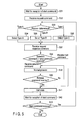
- FIG. 5 is a flowchart for illustrating another example of the process of the IC card 2 shown in FIG. 2 .
- Steps S31 to S43 shown in FIG. 5 are the same as steps S11 to S23 shown in FIG. 4 .
- the operation of the IC card 2 shown in FIG. 5 is different in a process transition made when a start command is received in the halt state.
- step S41 when a halt command is received in step S38 or when a release command is received in step S40, the CPU 25 of the IC card 2 is set into a halt state (step S41).
- the IC card 2 When the IC card 2 is set into the halt state, it is set into a state to wait for reception of a start command (request command or wakeup command) again (step S42).
- step S43 When the CPU 25 receives a start command (YES in step S43) in step S42, it performs a process of step S33.
- the CPU 25 determines a communication protocol based on the received command (step S33). Further, the CPU 25 rewrites protocol information already stored in the RAM 27. That is, the CPU 25 stores information indicating a communication protocol of the command received in the halt state into the RAM 27.
- the communication protocols can be set in correspondence to applications.
- applications are stored in the nonvolatile memory 28.
- the nonvolatile memory 28 functions as a storage unit that stores a plurality of applications and management information items of the respective applications.
- an operational condition is added to management information of applications stored in the nonvolatile memory 28.
- Information for example, "selection time of communication protocol Type A", "selection time of communication protocol Type B” or the like is added to the above operational condition.
- the CPU 25 determines whether or not protocol information indicating Type A is stored in the RAM 27 at the execution time of the application A.
- the CPU 25 executes the application A only when protocol information indicating Type A is stored in the RAM 27.
- the applications that can be executed for the respective communication protocols can be limited.
- the IC card 2 suspends process of the channel A by the arbitrary commands on application.
- the IC card 2 can execute another application by use of the channel B.
- the IC card 2 performs respective processes in an independent state by setting status information indicating the state of progress of a process and protocol information indicating a selected communication protocol for each channel in the IC card 2.
- a mobile electronic device that can further enhance the convenience of the user and a control method of the mobile electronic device can be provided.
- the signal processor unit 243 has the configuration corresponding to the communication protocols of Type A, B, C.
- the configuration is not limited to the above configuration and may be a configuration corresponding to another communication system.
- the signal processor unit 243 has a signal processor unit corresponding to still another communication protocol.
Landscapes
- Engineering & Computer Science (AREA)
- Physics & Mathematics (AREA)
- General Physics & Mathematics (AREA)
- Computer Networks & Wireless Communication (AREA)
- Theoretical Computer Science (AREA)
- Health & Medical Sciences (AREA)
- Microelectronics & Electronic Packaging (AREA)
- Computer Hardware Design (AREA)
- Toxicology (AREA)
- Computer Security & Cryptography (AREA)
- Electromagnetism (AREA)
- General Health & Medical Sciences (AREA)
- Artificial Intelligence (AREA)
- Computer Vision & Pattern Recognition (AREA)
- Telephone Function (AREA)
- Near-Field Transmission Systems (AREA)
- Mobile Radio Communication Systems (AREA)
Applications Claiming Priority (1)
| Application Number | Priority Date | Filing Date | Title |
|---|---|---|---|
| JP2009067009A JP2010218453A (ja) | 2009-03-18 | 2009-03-18 | 携帯可能電子装置、及び携帯可能電子装置の制御方法 |
Publications (1)
| Publication Number | Publication Date |
|---|---|
| EP2230632A1 true EP2230632A1 (de) | 2010-09-22 |
Family
ID=42306683
Family Applications (1)
| Application Number | Title | Priority Date | Filing Date |
|---|---|---|---|
| EP09010984A Withdrawn EP2230632A1 (de) | 2009-03-18 | 2009-08-27 | Tragbare elektronische Vorrichtung und Steuerungsverfahren für eine tragbare elektronische Vorrichtung |
Country Status (4)
| Country | Link |
|---|---|
| US (1) | US20100240318A1 (de) |
| EP (1) | EP2230632A1 (de) |
| JP (1) | JP2010218453A (de) |
| SG (1) | SG165219A1 (de) |
Families Citing this family (6)
| Publication number | Priority date | Publication date | Assignee | Title |
|---|---|---|---|---|
| US9048819B2 (en) * | 2006-11-18 | 2015-06-02 | RF Micron, Inc. | Method and apparatus for detecting RF field strength |
| JP4910035B2 (ja) * | 2009-11-13 | 2012-04-04 | 株式会社東芝 | 電子機器および通信制御方法 |
| FR2961619B1 (fr) * | 2010-06-22 | 2012-08-31 | St Microelectronics Rousset | Procede de gestion de la communication entre un dispositif electronique, par exemple une carte a puce sans contact, et un appareil de communication, par exemple un lecteur, et dispositif electronique correspondant |
| US9053248B2 (en) | 2012-08-31 | 2015-06-09 | Nxp B.V. | SRAM handshake |
| US9514067B2 (en) * | 2012-08-31 | 2016-12-06 | Nxp B.V. | Interface arbitration for a wired tag |
| JP6946027B2 (ja) * | 2017-03-17 | 2021-10-06 | 株式会社東芝 | Icカード、携帯可能電子装置、プログラム、処理装置及び処理システム |
Citations (4)
| Publication number | Priority date | Publication date | Assignee | Title |
|---|---|---|---|---|
| JP2001312699A (ja) | 2000-04-28 | 2001-11-09 | Denso Corp | 非接触式icカード用リーダライタ |
| FR2831305A1 (fr) | 2001-10-23 | 2003-04-25 | Inside Technologies | Circuit integre sans contact comprenant des moyens d'identification automatique de trame |
| WO2006110000A1 (en) | 2005-04-15 | 2006-10-19 | Ktfreetel Co., Ltd. | Contactless type integrated circuit card and method for communicating data by multiprotocol |
| EP2012257A2 (de) | 2007-06-27 | 2009-01-07 | Hitachi, Ltd. | Kontaktfreie elektronische Vorrichtung |
Family Cites Families (7)
| Publication number | Priority date | Publication date | Assignee | Title |
|---|---|---|---|---|
| JP2000172806A (ja) * | 1998-12-08 | 2000-06-23 | Hitachi Ltd | 非接触icカード |
| JP3881844B2 (ja) * | 2000-12-18 | 2007-02-14 | Necトーキン株式会社 | 非接触型icカード |
| KR100560770B1 (ko) * | 2003-09-15 | 2006-03-13 | 삼성전자주식회사 | 실시간 프로토콜 전환 기능을 갖는 비접촉 집적회로 카드및 그것을 포함한 카드 시스템 |
| JP2006099324A (ja) * | 2004-09-29 | 2006-04-13 | Matsushita Electric Ind Co Ltd | 非接触カード |
| JP4891708B2 (ja) * | 2006-08-31 | 2012-03-07 | 株式会社東芝 | 情報通信媒体 |
| US7971048B2 (en) * | 2008-03-27 | 2011-06-28 | Intel Corporation | System and method for establishing a trust domain on a computer platform |
| US8408454B2 (en) * | 2008-09-16 | 2013-04-02 | Visa U.S.A. Inc. | Multifunctional portable consumer payment device |
-
2009
- 2009-03-18 JP JP2009067009A patent/JP2010218453A/ja active Pending
- 2009-08-25 SG SG200905716-7A patent/SG165219A1/en unknown
- 2009-08-27 US US12/548,875 patent/US20100240318A1/en not_active Abandoned
- 2009-08-27 EP EP09010984A patent/EP2230632A1/de not_active Withdrawn
Patent Citations (4)
| Publication number | Priority date | Publication date | Assignee | Title |
|---|---|---|---|---|
| JP2001312699A (ja) | 2000-04-28 | 2001-11-09 | Denso Corp | 非接触式icカード用リーダライタ |
| FR2831305A1 (fr) | 2001-10-23 | 2003-04-25 | Inside Technologies | Circuit integre sans contact comprenant des moyens d'identification automatique de trame |
| WO2006110000A1 (en) | 2005-04-15 | 2006-10-19 | Ktfreetel Co., Ltd. | Contactless type integrated circuit card and method for communicating data by multiprotocol |
| EP2012257A2 (de) | 2007-06-27 | 2009-01-07 | Hitachi, Ltd. | Kontaktfreie elektronische Vorrichtung |
Also Published As
| Publication number | Publication date |
|---|---|
| SG165219A1 (en) | 2010-10-28 |
| US20100240318A1 (en) | 2010-09-23 |
| JP2010218453A (ja) | 2010-09-30 |
Similar Documents
| Publication | Publication Date | Title |
|---|---|---|
| EP2230632A1 (de) | Tragbare elektronische Vorrichtung und Steuerungsverfahren für eine tragbare elektronische Vorrichtung | |
| US8931705B2 (en) | IC card, mobile electronic device and data processing method in IC card | |
| US8123136B2 (en) | Processing apparatus of portable electronic devices, portable electronic device, and processing system of portable electronic devices | |
| EP2500845A2 (de) | Tragbare elektronische Vorrichtung | |
| JP2017126125A (ja) | Icカード、携帯可能電子装置及び処理装置 | |
| JP5823109B2 (ja) | 携帯可能電子装置、及び携帯可能電子装置の制御方法 | |
| JP2007087168A (ja) | 複合携帯可能電子装置および複合icカード | |
| JP2011022841A (ja) | 携帯可能電子装置の処理システム、携帯可能電子装置、及び携帯可能電子装置の処理装置 | |
| US20110181388A1 (en) | Portable electronic device and method for controlling portable electronic device | |
| JP2011065477A (ja) | 携帯可能電子装置 | |
| JP5693824B2 (ja) | Icカードの処理装置、icカード、及びicカードの処理システム | |
| JP2012008888A (ja) | 通信システム、通信方法及び携帯可能電子装置 | |
| JP7366765B2 (ja) | Icカード、icカード処理システム、及びicカード処理装置の制御プログラム | |
| JP6092342B2 (ja) | 非接触式携帯可能電子装置、及び非接触式携帯可能電子装置の発行方法 | |
| JP2014109973A (ja) | 通信媒体 | |
| WO2021124846A1 (ja) | Icカード及びicカードの制御プログラム | |
| JP2012190421A (ja) | 携帯可能電子装置、及び携帯可能電子装置の制御方法 | |
| KR101485157B1 (ko) | 입력장치를 갖는 무선식별 태그 | |
| JP2012194698A (ja) | 携帯可能電子装置、携帯可能電子装置の処理装置、及び携帯可能電子装置の処理システム | |
| JP2004192253A (ja) | Icカード及びicカードプログラム | |
| JP2009187495A (ja) | 情報処理装置、情報処理方法及びプログラム | |
| JP2008276572A (ja) | 非接触式icカード | |
| JP5875772B2 (ja) | 携帯可能電子装置、携帯可能電子装置の制御方法、及び携帯可能電子装置の処理システム | |
| JP2018022228A (ja) | 電子情報記憶媒体、判定方法、及び判定プログラム | |
| JP5726659B2 (ja) | Icカード、icカードの処理装置、及びicカードの処理システム |
Legal Events
| Date | Code | Title | Description |
|---|---|---|---|
| PUAI | Public reference made under article 153(3) epc to a published international application that has entered the european phase |
Free format text: ORIGINAL CODE: 0009012 |
|
| 17P | Request for examination filed |
Effective date: 20090827 |
|
| AK | Designated contracting states |
Kind code of ref document: A1 Designated state(s): AT BE BG CH CY CZ DE DK EE ES FI FR GB GR HR HU IE IS IT LI LT LU LV MC MK MT NL NO PL PT RO SE SI SK SM TR |
|
| AX | Request for extension of the european patent |
Extension state: AL BA RS |
|
| STAA | Information on the status of an ep patent application or granted ep patent |
Free format text: STATUS: THE APPLICATION IS DEEMED TO BE WITHDRAWN |
|
| 18D | Application deemed to be withdrawn |
Effective date: 20130122 |