EP2227859B1 - Filterdesignverfahren und filter auf der basis von metamaterialstrukturen - Google Patents
Filterdesignverfahren und filter auf der basis von metamaterialstrukturen Download PDFInfo
- Publication number
- EP2227859B1 EP2227859B1 EP08851171.2A EP08851171A EP2227859B1 EP 2227859 B1 EP2227859 B1 EP 2227859B1 EP 08851171 A EP08851171 A EP 08851171A EP 2227859 B1 EP2227859 B1 EP 2227859B1
- Authority
- EP
- European Patent Office
- Prior art keywords
- cell
- crlh
- filter
- metallization layer
- band
- Prior art date
- Legal status (The legal status is an assumption and is not a legal conclusion. Google has not performed a legal analysis and makes no representation as to the accuracy of the status listed.)
- Active
Links
Images


Classifications
-
- H—ELECTRICITY
- H01—ELECTRIC ELEMENTS
- H01P—WAVEGUIDES; RESONATORS, LINES, OR OTHER DEVICES OF THE WAVEGUIDE TYPE
- H01P1/00—Auxiliary devices
- H01P1/20—Frequency-selective devices, e.g. filters
- H01P1/201—Filters for transverse electromagnetic waves
- H01P1/203—Strip line filters
-
- H—ELECTRICITY
- H03—ELECTRONIC CIRCUITRY
- H03H—IMPEDANCE NETWORKS, e.g. RESONANT CIRCUITS; RESONATORS
- H03H7/00—Multiple-port networks comprising only passive electrical elements as network components
- H03H7/01—Frequency selective two-port networks
-
- H—ELECTRICITY
- H01—ELECTRIC ELEMENTS
- H01P—WAVEGUIDES; RESONATORS, LINES, OR OTHER DEVICES OF THE WAVEGUIDE TYPE
- H01P1/00—Auxiliary devices
- H01P1/20—Frequency-selective devices, e.g. filters
- H01P1/213—Frequency-selective devices, e.g. filters combining or separating two or more different frequencies
-
- H—ELECTRICITY
- H01—ELECTRIC ELEMENTS
- H01P—WAVEGUIDES; RESONATORS, LINES, OR OTHER DEVICES OF THE WAVEGUIDE TYPE
- H01P3/00—Waveguides; Transmission lines of the waveguide type
- H01P3/02—Waveguides; Transmission lines of the waveguide type with two longitudinal conductors
- H01P3/08—Microstrips; Strip lines
Definitions
- a metamaterial has an artificial structure. When designed with a structural average unit cell size p much smaller than the wavelength of the electromagnetic energy guided by the metamaterial, the metamaterial can behave like a homogeneous medium to the guided electromagnetic energy. Unlike RH materials, a metamaterial can exhibit a negative refractive index with permittivity e and permeability [mu] being simultaneously negative, and the phase velocity direction is opposite to the direction of the signal energy propagation where the relative directions of the (E, H, ⁇ ) vector fields follow the left handed rule. Metamaterials that support only a negative index of refraction with permittivity ⁇ and permeability ⁇ being simultaneously negative are pure "left handed" (LH) metamaterials.
- CRLH metamaterials are mixtures of LH metamaterials and RH materials and thus are Composite Left and Right Handed (CRLH) metamaterials.
- a CRLH metamaterial can behave like a LH metamaterial at low frequencies and a RH material at high frequencies. Designs and properties of various CRLH metamaterials are described in, Caloz and Itoh, "Electromagnetic Metamaterials: Transmission Line Theory and Microwave Applications,” John Wiley & Sons (2006 ). CRLH metamaterials and their applications in antennas are described by Tatsuo Itoh in “Invited paper: Prospects for Metamaterials," Electronics Letters, Vol. 40, No. 16 (August, 2004 ).
- CRLH metamaterials can be structured and engineered to exhibit electromagnetic properties that are tailored for specific applications and can be used in applications where it may be difficult, impractical or infeasible to use other materials.
- CRLH metamaterials may be used to develop new applications and to construct new devices that may not be possible with RH materials.
- E-CRLH Extended composite right/left-handed metamaterial and its application as quadband quarter-wavelength transmission line
- Microwave Conference, 1 December 2006 Asia-Pacific, IEEE pages 1405-1408 discloses an extended composite right/left handed transmission line and its application as quadband quarter-wavelength transmission line which comprises a series inductor and a series capacitance of a conventional CRLH connected to a series inductor and a series capacitance of a dual CRLH and a shunt inductor and a shunt capacitance of a CRLH connected to a shunt inductor and a shunt capacitance of a dual CRLH.
- Three conditions are required for balance.
- the resonance frequency of the series inductor and series capacitance of the conventional CRLH is selected to be the same ( ⁇ o c ) as the resonance frequency of the shunt inductor and shunt capacitance of the conventional CRLH
- the resonance frequency of the series inductor and series capacitance of the dual CRLH is selected to be the same ( ⁇ o d ) as the resonance frequency of the shunt inductor and shunt capacitance of the dual CRLH
- ⁇ o c is chosen to be the same as ⁇ o d so that all four resonance frequencies are the same.
- This application describes filters based on metamaterial structures including an extended composite left and right handed (E-CRLH) metamaterial unit cell.
- E-CRLH extended composite left and right handed
- a filter apparatus comprising:-
- the E-CRLH unit cell has a printed circuit structure formed in four separated metallization layers which that are parallel to one another and comprise:
- the filter designs and design methods described here may be implemented to provide an optimum circuit based filter design utilizing a CRLH type structure that is efficient, easily scales to any band, can provide for matching conditions over a targeted frequency band, and also integrates into front-end module packages.
- the filter designs and design methods described here may be also be used to provide a Conventional and Extended structure of transmission-line based Composite Right-Left Handed, C-CRLH and E-CRLH respectively, Metamaterial (MTM) that generally exhibit rich dispersion behavior to allow better control one or more of the following filter characteristics: frequency bands, quality factor, sideband filter rejection, low insertion loss.
- MTM Metamaterial
- Metamaterial (MTM) structures can be used to construct antennas, transmission lines, filters and other electrical components and devices, allowing for a wide range of technology advancements such as size reduction and performance improvements.
- the MTM antenna structures can be fabricated on various circuit platforms, for example, a conventional FR-4 Printed Circuit Board (PCB) or a Flexible Printed Circuit (FPC) board.
- PCB FR-4 Printed Circuit Board
- FPC Flexible Printed Circuit
- Examples of other fabrication techniques include thin film fabrication technique, system on chip (SOC) technique, low temperature co-fired ceramic (LTCC) technique, and monolithic microwave integrated circuit (MMIC) technique.
- CRLH metamaterial structure In one application of CRLH metamaterial structure, such structures can be directly applied to modern filter designs.
- Filter design in general, enables communication links to filter out any signals from frequency bands other than the one used to communicate.
- Modern filter designs and techniques utilizing CRLH structures may be a high-pass, band-pass, or impedance transformer some of which are described by G. Mattaei, L. Young, E. N. T. Jones, "Microwave Filters, Impedance-matching Networks, and Coupling Structures", Artech House publisher, 1980 .
- the high-pass design filter is based on pure left-handed unit cells as described by Mattaei.
- the band-pass and impedance transformer design filters are based on CRLH unit cells.
- the use of the CRLH structure filter design is difficult to achieve in a practical microwave structure and, instead, series inductances and impedance inverters are used for filter design.
- a high number of unit cells such as Conventional CRLH (C-CRLH) are required to create sharp filters which increases filter insertion loss due to ripples appearing in the filter pass band.
- C-CRLH Conventional CRLH
- the unit cell parameters and number of cells are derived from coefficients listed in tables generated for different unit cells.
- Alternative approaches to filter designs are also available but generally utilize brute force techniques to achieve optimum results.
- E-CRLH Extended Composite Right/Left-Handed
- a practical limitation of current filter designs is their inability to simplify the RF Front End Module (FEM) of small wireless communication devices, such as handsets and client cards.
- FEM RF Front End Module
- SAW Surface Acoustic Wave
- the present application discloses examples and implementations of filter designs and filters based on MTM structures.
- the MTM structures for filters can be based on MTM antenna structures and MTM transmission line structures, which can be configured to generate two different frequency bands: a "low band” and a "high band.”
- the low band includes at least one left-handed (LH) mode resonance and the high band includes at least one right-handed (RH) mode resonance.
- LH left-handed
- RH right-handed
- Some of the implementations in the present application are directed to cell phone applications, handheld device applications (e.g., Blackberry) and other mobile device applications, in which the antenna is expected to support multiple frequency bands with adequate performance under limited space constraints.
- the MTM antenna designs disclosed in the present application provide advantages over conventional antennas such as but not limited to smaller sizes, multiple resonances based on a single antenna solution, stable resonances that do not shift with the user interaction and resonant frequencies that are independent of the physical size.
- the frequency bands in cell phone and mobile device applications are comprised of: the cellular band (824 - 960MHz) which actually includes two bands, CDMA and GSM bands; and the PCS/DCS band (1710 - 2170 MHz) which actually includes three bands: PCS, DCS and WCDMA bands.
- a quad-band antenna covers one of the CDMA and GSM bands in the cellular band and all three bands in the PCS/DCS band.
- a penta-band antenna covers all five bands (two in the cellular band and three in the PCS/DCS band) .
- Exemplary MTM antenna structures are described in U.S. Patent Application No. 11/741,674 entitled “Antennas, Devices, and Systems Based on Metamaterial Structures,” filed on April 27, 2007, and U.S. Patent Application No. 11/844,982 entitled “Antennas Based on Metamaterial Structures,” filed on August 24, 2007.
- An MTM antenna or MTM transmission line is a MTM structure with one or more MTM unit cells.
- the equivalent circuit for each MTM unit cell includes a right-handed series inductance (LR), a right-handed shunt capacitance (CR), a left-handed series capacitance (CL), and a left-handed shunt inductance (LL).
- LL and CL are structured and connected to provide the left-handed properties to the unit cell.
- This type of CRLH TLs or antennas can be implemented by using distributed circuit elements, lumped circuit elements or a combination of both.
- Each unit cell is smaller than about ⁇ /4 where ⁇ is the wavelength of the electromagnetic signal that is transmitted in the CRLH TL or antenna.
- a pure LH metamaterial follows the left-hand rule for the vector trio ( E,H, ⁇ ), and the phase velocity direction is opposite to the signal energy propagation. Both the permittivity ⁇ and permeability ⁇ of the LH material are negative.
- a CRLH metamaterial can exhibit both left-hand and right-hand electromagnetic modes of propagation depending on the regime or frequency of operation. Under certain circumstances, a CRLH metamaterial can exhibit a non-zero group velocity when the wavevector of a signal is zero. This situation occurs when both left-hand and right-hand modes are balanced. In an unbalanced mode, there is a bandgap in which electromagnetic wave propagation is forbidden.
- ⁇ ⁇ , while the group velocity is positive: v g d ⁇ d ⁇
- ⁇ 0 > 0.
- the CRHL structure supports a fine spectrum of low frequencies with the dispersion relation that follows the negative P parabolic region. This allows a physically small device to be built that is electromagnetically large with unique capabilities in manipulating and controlling near-field radiation patterns.
- This TL When this TL is used as a Zeroth Order Resonator (ZOR), it allows a constant amplitude and phase resonance across the entire resonator.
- the ZOR mode can be used to build MTM-based power combiners and splitters or dividers, directional couplers, matching networks, and leaky wave antennas.
- the TL length should be long to reach low and wider spectrum of resonant frequencies.
- the operating frequencies of a pure LH material are at low frequencies.
- a CRLH MTM structure is very different from an RH or LH material and can be used to reach both high and low spectral regions of the RF spectral ranges.
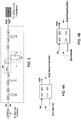
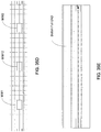
- FIG. 1 illustrates an example of a 1D CRLH MTM TL based on four unit cells.
- One unit cell includes a cell patch and a via, and is a minimum unit that repeats itself to build the MTM structure.
- the four cell patches are placed on a substrate with respective centered vias connected to the ground plane.
- FIG. 2 shows an equivalent network circuit of the 1D CRLH MTM TL in FIG. 1 .
- the ZLin' and ZLout' correspond to the TL input load impedance and TL output load impedance, respectively, and are due to the TL coupling at each end.
- This is an example of a printed two-layer structure.
- LR is due to the cell patch on the dielectric substrate
- CR is due to the dielectric substrate being sandwiched between the cell patch and the ground plane.
- CL is due to the presence of two adjacent cell patches, and the via induces LL.
- Each individual unit cell can have two resonances ⁇ SE and ⁇ SH corresponding to the series (SE) impedance Z and shunt (SH) admittance Y.
- the Z/2 block includes a series combination of LR/2 and 2CL
- the Y block includes a parallel combination of LL and CR.
- ⁇ SH 1 LL CR
- ⁇ SE 1 LR CL
- ⁇ R 1 LR CR
- ⁇ L 1 LL CL
- Z j ⁇ LR + 1 j ⁇ CL
- Y j ⁇ CR + 1 j ⁇ LL
- the two unit cells at the input/output edges in FIG. 1 do not include CL, since CL represents the capacitance between two adjacent cell patches and is missing at these input/output edges.
- CL represents the capacitance between two adjacent cell patches and is missing at these input/output edges.
- ZLin and ZLout' series capacitor are included to compensate for the missing CL portion, and the remaining input and output load impedances are denoted as ZLin and ZLout, respectively, as seen in FIG. 3 .
- all unit cells have identical parameters as represented by two series Z/2 blocks and one shunt Y block in FIG.3 , where the Z/2 block includes a series combination of LR/2 and 2CL, and the Y block includes a parallel combination of LL and CR.
- FIG. 4A and FIG. 4B illustrate a two-port network matrix representation for TL circuits without the load impedances as shown in FIG. 2 and FIG. 3 , respectively,
- FIG. 5 illustrates an example of a 1D CRLH MTM antenna based on four unit cells.
- FIG. 6A shows a two-port network matrix representation for the antenna circuit in FIG 5.
- FIG. 6B shows a two-port network matrix representation for the antenna circuit in FIG 5 with the modification at the edges to account for the missing CL portion to have all the unit cells identical.
- FIGS. 6A and 6B are analogous to the TL circuits shown in FIGS. 4A and 4B , respectively.
- the parameters GR' and GR represent a radiation resistance
- the parameters ZT' and ZT represent a termination impedance.
- Each of ZT', ZLin' and ZLout' includes a contribution from the additional 2CL as expressed below:
- ZLin ′ ZLin + 2 j ⁇ CL
- ZLout ′ ZLout + 2 j ⁇ CL
- ZT ′ ZT + 2 j ⁇ CL .
- each of the N CRLH cells is represented by Z and Y in Eq. (1), which is different from the structure shown in FIG. 2 , where CL is missing from end cells. Therefore, one might expect that the resonances associated with these two structures are different.
- Z and Y are given in Eq.
- >0 are the same regardless if the full CL is present at the edge cells ( FIG. 3 ) or absent ( FIG. 2 ). Furthermore, resonances close to n 0 have small ⁇ values (near ⁇ lower bound 0), whereas higher-order resonances tend to reach ⁇ upper bound 4 as stated in Eq. (4).
- the limiting frequencies ⁇ min and ⁇ max values are given by the same resonance equations in Eq.
- FIGS. 7A and 7B provide examples of the resonance position along the dispersion curves.
- the structure size l Np, where p is the cell size, increases with decreasing frequency.
- the LH region lower frequencies are reached with smaller values of Np, hence size reduction.
- the dispersion curves provide some indication of the bandwidth around these resonances. For instance, LH resonances have the narrow bandwidth because the dispersion curves are almost flat. In the RH region, the bandwidth is wider because the dispersion curves are steeper.
- res 2 ⁇ ⁇ n ⁇ R 2 1 ⁇ ⁇ SE 2 ⁇ SH 2 ⁇ ⁇ n 4 , where ⁇ is given in Eq.
- Eq. (1) The dispersion relation in Eq. (4) indicates that resonances occur when
- 1, which leads to a zero denominator in the 1 st BB condition (COND1) of Eq. (7).
- COND1 the 1 st BB condition
- AN is the first transmission matrix entry of the N identical unit cells ( FIG. 4B and FIG. 6B ).
- COND1 is indeed independent of N and given by the second equation in Eq. (7).
- It is the values of the numerator and ⁇ at resonances, which are shown in Table 1, that define the slopes of the dispersion curves, and hence possible bandwidths. Targeted structures are at most Np ⁇ /40 in size with the bandwidth exceeding 4%.
- Eq. (7) indicates that high ⁇ R values satisfy COND1, i.e., low CR and LR values, since for n ⁇ 0 resonances occur at ⁇ values near 4 in Table 1, in other terms (1- ⁇ /4 ⁇ 0).
- B1/C1 is greater than zero is due to the condition of
- ⁇ 1 in Eq. (4), which leads to the following impedance condition: 0 ⁇ ⁇ ZY ⁇ ⁇ 4.
- the 2 nd broadband (BB) condition is for Zin to slightly vary with frequency near resonances in order to maintain constant matching.
- the 2 nd BB condition is given below: COND 2 : 2 ed BB condition : near resonances , d Zin d ⁇
- antenna designs have an open-ended side with an infinite impedance which poorly matches the structure edge impedance.
- the shunt capacitor CR should be reduced. This reduction can lead to higher ⁇ R values of steeper dispersion curves as explained in Eq. (7).
- FIGS. 1 and 5 use a conductive layer to cover the entire bottom surface of the substrate as the full ground electrode.
- a truncated ground electrode that has been patterned to expose one or more portions of the substrate surface can be used to reduce the area of the ground electrode to less than that of the full substrate surface. This can increase the resonant bandwidth and tune the resonant frequency.
- Two examples of a truncated ground structure are discussed with reference to FIGS. 8 and 11 , where the amount of the ground electrode in the area in the footprint of a cell patch on the ground electrode side of the substrate has been reduced, and a remaining strip line (via line) is used to connect the via of the cell patch to a main ground electrode outside the footprint of the cell patch.
- This truncated ground approach may be implemented in various configurations to achieve broadband resonances.
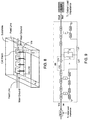
- FIG. 8 illustrates one example of a truncated ground electrode for a four-cell transmission line where the ground has a dimension that is less than the cell patch along one direction underneath the cell patch.
- the ground conductive layer includes a via line that is connected to the vias and passes through underneath the cell patches.
- the via line has a width that is less than a dimension of the cell path of each unit cell.
- the use of a truncated ground may be a preferred choice over other methods in implementations of commercial devices where the substrate thickness cannot be increased or the cell patch area cannot be reduced because of the associated decrease in antenna efficiencies.
- another inductor Lp FIG.
- FIG. 10 shows a four-cell antenna counterpart with the truncated ground analogous to the TL structure in FIG. 8 .
- FIG. 11 illustrates another example of a truncated ground structure.
- the ground conductive layer includes via lines and a main ground that is formed outside the footprint of the cell patches.
- Each via line is connected to the main ground at a first distal end and is connected to the via at a second distal end.
- the via line has a width that is less than a dimension of the cell path of each unit cell.
- a design approach is provided and shown in FIG. 13 for optimizing and verifying filter designs with or without MTM structures. Steps 1 through 6, described below, provide a process methodology to extract circuit parameters that are considered in the filter designs listed in Table 2.
- FIG. 14 One application of the filter designs described in Table 2 is in wireless network systems.
- these filter designs can be applied to a Wireless Local Area Network (WLAN) and a Wireless Wide Area Network (WWAN) diplexer system as discussed in U.S. Patent application Serial No. 61/050,954 entitled "Single Cable Antenna Solution for Laptop Computer” and filed on May 6, 2008.
- WLAN Wireless Local Area Network
- WWAN Wireless Wide Area Network
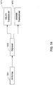
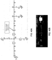
- it may be desirable to combine and split the WLAN and WWAN signals and route them to their corresponding radio transceivers as illustrated in FIG. 14 for example, where a functional block diagram of a diplexer 1405 is connected to an antenna 1401 and a WLAN 1411 and WWAN 1415 transceivers. Since both WWAN and WLAN radios share a single antenna, the diplexer is responsible to split and combine WWAN and WLAN signals to and from their corresponding transceivers, respectively.
- Such a diplexer apparatus can include a main input/output port capable of transmitting and receiving a plurality of signals having a low-band frequency range and a high-band frequency range, a low-band input/output port capable of transmitting and receiving a first signal operating at the low-band frequency, a low-pass filter connecting the main input/output port to the low-band input/output port having a low insertion loss and a sharp upper band edge; a high-band input/output port capable of transmitting and receiving a second signal operating at the high-band frequency; and a high-pass filter connecting the main input/output port to the high-band port having a low insertion and a sharp lower band edge.
- the isolation defined between the upper edge of the low-band filter and the lower edge of the high-band filter defines is low. As an example, the isolation may be below -25dB in some applications.
- the diplexer can be designed using a low-pass filter and a high-pass filter which can have a sharp side band rejection between the two filters as illustrated in the S12 responses as a function of the frequency shown in FIGS. 15A and 15B , respectively.
- the low-pass filter generally covers the WWAN frequency band 800-2170 MHz and has an insertion loss that is less than 1dB while the high-pass filter typically covers the WLAN frequency band 2.3-6.0 GHz and has an insertion loss that is less than 1dB.
- the side band rejection restriction is such that the WWAN filter can be better than -20 dB at 2.3 GHz and the WLAN filter can be better than -15 dB, -20 dB, and -25 dB rejection at 2.17 GHz, 1.575 GHz, and .825 GHz respectively.
- E-CRLH Extended Composite Right Left Handed single cell
- This E-CRLH cell includes a series inductor LR and a series capacitance CL that in combination produce a series resonance ⁇ SE , a shunt inductor LL and a shunt capacitance CR that in combination produce a shunt resonance ⁇ SH , a series inductor LR' and a series capacitance CL' that in combination produce a series resonance ⁇ SE' , and a shunt inductor LL' and a shunt capacitance CR' that in combination produce a shunt resonance ⁇ SH' .
- the circuit elements in this E-CRLH cell are arranged to form a symmetric cell structure for the E-CRLH unit cell where the input and output of the E-CRLH unit cell have a common circuit structure.
- the series inductor LR, the series capacitance CL, the shunt inductor LL, the shunt capacitance CR, the series inductor LR', the series capacitance CL', the shunt inductor LL' and the shunt capacitance CR' are selected to have values that render ⁇ SE and ⁇ SH' to be substantially equal, and ⁇ SH and ⁇ SE' to be substantially equal.
- the E-CRLH cell in FIG. 16C can be viewed as a non-linear combination of a Conventional CRLH (C-CRLH) cell ( FIG. 16A ) and its Dual CRLH (D-CRLH) cell ( FIG. 16B ).
- C-CRLH Conventional CRLH
- D-CRLH Dual CRLH
- a C-CRLH structure resonates in the LH region at low frequency bands and resonates in the RH region at high frequency bands.
- the C-CRLH structure effectively behaves like a band-pass filter that gets sharper as the number of cells is increased. Increasing the number of cells can lead to undesirable conditions such as an increase in transmission loss and larger structure sizes.
- a D-CRLH structure unlike the C-CRLH structure, resonates in the RH region at low frequencies, resonates in the LH region at high frequencies, and acts like stop-band filter.
- C-CRLH and D-CRLH structures can be combined linearly because each is easier to analyze and implement than the E-CRLH structure, however, this linear combination generally yields to structures that are dominated by the stop-band feature associated with the D-CRLH structure rather than the band-pass properties of C-CRLH.
- E-CRLH filter designs Four zero order ⁇ 01 , ⁇ 02 , ⁇ 03 , and ⁇ 04 resonances that an E-CRLH cell exhibits are listed below in Eq. (12) and Eq. (13). Examples of a fully printed E-CRLH design ( Figs. 27A-E : and Fig. 17 ) and a fully discrete E-CRLH design with pads for components ( Fig. 18 ) are illustrated. Alternatively, a hybrid printed/discrete structure can also be used to realize E-CRLH filter designs.
- FIG. 16C An example of a broadband filter using the E-CRLH structure is illustrated in FIG. 16C .
- the values of the corresponding circuit parameters are listed in the table below, while the filter responses of the E-CRLH unit cell and E-CRLH unit cell with LP are depicted in FIG. 19 and FIG. 20B , respectively.
- a 1-cell E-CRLH filter spans the range of about 0.89GHz to 2.23 GHz at -3dB and has a sharp side band rejection edge on the upper edge of the band.
- a LP pass can be added after the main E-CRLH filter.
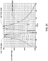
- the response plot of the LP filter is illustrated in FIG. 21B .
- the upper edge of the LP filter is about 2.3 GHz at -3dB making it a good candidate to eliminate bands above 2.3 GHz in the main filter response shown in FIG. 19 .
- the combined 1-cell E-CRLH 2001 and 3-cell LP filter circuit 2005 is illustrated in FIG. 20A and its response plot is illustrated in FIG. 20B .
- only the lower band, with its sharp upper filter band edge may be achieved while maintaining near zero insertion loss (i.e., no ripples).
- a low-pass post-filter may be used to eliminate all bands higher than 3GHz.
- An example of a 3-cell Low-Pass (LP) filter is provided in FIG. 21A .
- the present techniques and filters may be configured to address such challenges in context of an unbalanced extended design where an E-CRLH is used as part of the design and construction of a high-Q filter.
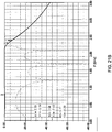
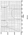
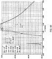
- FIG. 22 depicts an example of an E-CRLH beta curve.
- the E-CRLH design may start with low-frequency resonances in the 260 MHz band, and then move to the RH region to excite the 390 MHz band. Subsequently, the dispersion curve can move back to the LH region to excite the 780 MHz band before continuing in the RH region.
- FIG. 23 illustrates a flow chart that represents the methodology and steps needed to design and construct all printed, discrete, or hybrid printed/discrete E-CRLH structure.
- step 1 2301 requires identifying four bands Freq1, Freq2, Freq3, Freq4 and a subset of four of the eight structure parameters CL, LR, LL, CR, CL', LR', LL', CR'.
- the target filter bands are specified by the four frequency inputs and the rest of the four independent parameters selected from CL, LR, LL, CR, CL', LR', LL', CR' are used to match the structure at these target frequency bands.
- Step 2 2305 requires deriving the rest of the four dependent parameters followed by using one of the irrelevant independent parameters to tune the input impedance to the desired value.
- Step 4 2311, step 5 2315, and step 6 2321 involves constructing various E-CRLH structures such as a discrete component, a multi-layer printed GE-CRLH structure, and a hybrid discrete printed structure, respectively.
- the E-CRLH rich dispersion characteristics can provide a unique means to manipulate its dispersion curves to excite a higher number of frequency bands with target values of Q (bandwidth).
- a high-Q filter can be used to enable wireless communication devices to operate over very narrow bands without interfering with adjacent bands.
- a proprietary parameter extraction software can be used to derive the rest of the parameters:
- FIG. 22 illustrates a dispersion curve of the circuit shown in FIG. 18 .
- This chart suggests that a given constraint in designing such a structure is exciting high-Q bands, which can be easily seen by the near-flat beta curves at the three desired 260 MHz, 390 MHz, and 780 MHz bands.
- One advantage of such a design is the ability to match the three bands with a 50 Ohm input impedance feed-line.
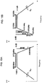
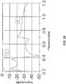
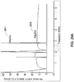
- FIG. 25 A photograph of a preliminary 1-cell E-CRLH fabrication is illustrated in FIG. 25 .
- the goal of fabricating this structure is intended to demonstrate the existence of these three resonances rather than optimize losses.
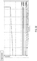
- FIG. 26 illustrates measured results for S11 and S12. By comparing the simulated results in Table 5 to the measured results in FIG. 26 , it is apparent that the three resonances 236 MHz, 400 MHz, and 704 MHz are very close to the theoretical model.
- a high-pass post-filter can be used to eliminate the lower two bands, 236 MHz and 400 MHz, and preserve the 700MHz bandpass.
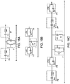
- FIG. 17 An example of fully printed E-CRLH structure is illustrated in FIG. 17 , and is based on a 4-layer design as illustrated in FIGS. 27A-27E and detailed in Table 7.
- This particular E-CRLH unit cell has a printed circuit structure formed in four separated metallization layers which that are parallel to one another.
- the first metallization layer is patterned to comprise a first signal port, a first feed line coupled to the first signal port, a first launch pad coupled to the first feed line, and a first cell patch that is separated from and capacitively coupled to the first launch pad, a second cell patch spaced from the first cell patch and coupled to receive a signal from the first cell patch, a second launch pad separated from and capacitively coupled to the second cell patch, a second feed line coupled to the second launch pad, and a second signal port coupled to the second feed line.
- the second metallization layer is patterned to comprise a first conductive cell patch positioned underneath the first metallization layer between the first and second cell patches and to enhance electromagnetic coupling across the gap.
- the third metallization layer is patterned to comprise a second conductive cell underneath the first conductive cell patch in the second metallization layer.
- the first conductive via is provided to connect the first conductive cell patch in the second metallization layer and the second conductive cell patch in the third metallization layer.
- This design also includes a fourth metallization layer to provide a ground electrode for the apparatus, a first cell via and a second cell via between the first metallization layer and the ground electrode.
- the first cell via connects the first cell patch on the first metallization layer and the ground electrode in the fourth metallization layer and is separate from and without direct contact with the first and second conductive cell patches.
- the second cell via connects the second cell patch on the first metallization layer and the ground electrode in the fourth metallization layer, is separate from and without direct contact with the first and second conductive cell patches.
- Vias connecting inter-layer metallization are commonly referred to by "buried vias," such as the via Via 21 between the second and the third layers.
- buried vias such as the via Via 21 between the second and the third layers.
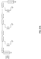
- the first metallization layer is patterned to comprise a first top ground electrode adjacent to the first launch pad and a second top ground electrode adjacent to the second launch pad and the second metallization layer is patterned to comprise a first bottom ground electrode underneath the first top ground electrode and a second bottom ground electrode underneath the second top ground electrode.
- the first top ground electrode is patterned to support, in combination with the first bottom ground electrode, a first co-planar waveguide (CPW) that is coupled between the first signal port and the first feed line
- the second top ground electrode is patterned to support, in combination with the second bottom ground electrode, a second CPW that is coupled between the second signal port and the second feed line.
- CPW co-planar waveguide
- Layer 1 Top Layer CPW feed line 15 mm long 50 Ohm line grounded CPW line with CPW-GND located on layer 2 layer 2 Launch Pad (LP) Section1: 0.5x2mm; Section2: 3x1mm; Section3: 8x3mm, gap between LP and Cell 11 is 0.1mm Cellll & Cell 12 8mm wide and 15 mm long Substrate 1 80mm long - Via 11 with 12mil diameter and located at 15 mm from left GND edge 45 mm wide 0.787 mm thick - Via 12 with 12mil diameter and located at 15mm from right GND edge CPW GND 45mm wide and 17.9mm long Cell 21 8 mm wide and 24 mm long located at 10.1mm from left GND in layer 2 Layer 2 GND Line Connects Bottom Cell Patch with the main GND Substrate 2 80mm long - Via 11 with 12mil diameter and located at 15 mm from left GND edge 45 mm wide - Via 12 with 12mil diameter and located at 15 15 mm from left GND
- Z and Y equations can be simplified leading to a simpler Zc function for improved matching.
- a excel sheet can be tailored to satisfy the above constraints. In this design, the following filter characteristics are observed and noted.
- the special case of the E-CRLH complying with equation (14B) mentioned above is applied to design the two filters that constitute the previously presented diplexer shown in FIG. 14 .
- the E-CRLH filter parameters are listed in Table 8 and Table 9.
- Table 8 E-CRLH filter parameters of FIG 16C Parameter Value Units Value Zc 15 ohm 15ohm LRover2 1.5/2 nH 0.75nH CR 2.6 pF 2.6pF LL 2.4 nH 2.4nH TwoCL 2*3.85 pF 7.7pF LRPover2 0.63/2 nH 0.315nH TwoCLP 2*10 pF 20pF LLP 5.8 nH 5.8nH CRP 1 pF 1pF
- the two frequencies Freq0_1, Freq_02, LR, CR, and LL' are considered the free parameters, whereas the rest Freq0_3, Freq0_4, LR', CR', LL, CL, and CL' are derived from the constraints in Eq (14B).
- a simple low-pass filter with less than -15dB at 2.1 GHz can be used to select the lower band-pass filter range of about 700 MHz to 1.89 GHz with a side-band rejection of about -40dB at 2 GHz.
- a simple high-pass filter with less than - 15dB at 2.1 GHz can be used to select the upper band-pass filter range of about 2.23 MHz to 5.92 GHz with side-band rejection of about -40dB at 2.1 GHz.
- narrower band filters can be derived using the special E-CRLH case complying with the constraints in Eq (14A).
- the E-CRLH filter parameters and corresponding circuit parameters are listed in Table 10 and Table 11, respectively.
- Table 10 E-CRLH filter parameters Parameter Value Units Value Zc 25 ohm 25ohm LRover2 120/2 nH 60nH CR 29 pF 29 pF LRPover2 1.2/2 nH 0.6nH LL 0.22 nH 0.22nH TwoCL 2*0.05 pF 0.1pF LLP 22 nH 22nH
- the matlab code provides two narrow-band band-pass regions.
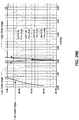
- the upper region can.be matched at about 25 Ohms as illustrated in FIG. 30 , while the lower-band shows a better matching at 45 Ohms.
- the structure needs to be matched to the input/output impedance Zc. That means the Real part of the impedance Re(Zc) needs to be near constant while keeping its imaginary (reactive)part Im(Zc)near zero.
- the Ansoft designer circuit simulation software provides a structure response as illustrated in FIG. 16C .
- a simple high-pass filter with less than -15dB at about 2.1 GHz can be used to select the upper band-pass filter range of about 2.11 MHz to 2.17 GHz with a side-band rejection below -40dB at about 2.05 GHz. Similar steps can be followed to match the lower band-pass region to select it. In this case, a 40 Ohm matching is more desirable as illustrated in the Matlab impedance results of FIG. 31 .
- C-CRLH Composite Right Left Handed
- TL Transmission Line
- each cell Cell 1 3201 and Cell 2 3205
- C-CRLH Composite Right Left Handed
- the special case when both cells are identical or “isotropic" case was analyzed in the previous sections and also covered by Caloz and Itoh, "Electromagnetic Metamaterials", book published by Wiley Publishing company, 2006 .
- the C-CRLH structure resonates in the LH region at low frequency bands and resonates in the RH region at high frequency bands.
- the C-CRLH structure effectively behaves like a band-pass filter that gets sharper as the number of cells is increased. Increasing the number of cells, however, can lead to undesirable conditions such as an increase in transmission loss and larger structure sizes.
- the MTM filter structure may be configured in context of a balanced conventional design.
- two designs in this section target the WWAN filter of the WLAN/WWAN diplexer application illustrated in FIGS. 14 , 15A, and 15B .
- Steps for designing the WWAN filter are as follows:
- the MTM cell structure includes a top conductive layer below the cell patch and the top ground in a metal-insulator-metal (MIM) structure, and a bottom MIM layer below the cell patch and the bottom ground.
- MIM metal-insulator-metal
- This MTM cell design is implemented by using five metallization layers with four inter-layer dielectric insulator layers.
- the layer 3 shown in FIG. 35C includes two cells 1 and 2 where each cell includes two cell patches that are connected to each other by a LR line which has an extension as the LL line leading to a via pad.
- the four inter-layer dielectric insulator layers may be implemented by, for example, four dielectric substrates. Vias connecting inter-layer metallization are commonly referred to by "buried vias". In some fabrication techniques, it is challenging to align buried vias when assembling the substrates on top of each other, hence the need to use "though vias" from top to bottom layers. This is accomplished by clearing metallization around "pass through vias" on layers the vias are not connected to the metallization on these layers.
- the C-CRLH) structure in FIGS. 35A-35E includes a top layer having a plurality of CPW feed lines, a top ground, and a plurality of ports and a first dielectric substrate having a first surface on a first side and a second surface on a second side opposing the first side.
- the first surface of the first substrate is attached to the top layer.
- a second layer having a top metal-insulator-metal (MIM) layer is provided.
- the second layer is attached to the second surface of the first substrate, and a first set of cell conductive via connectors are formed in the first substrate creating a conductive path from the top layer to the second layer.
- MIM metal-insulator-metal
- a second dielectric substrate is provided to have a first surface on a first side and a second surface on a second side opposing the first side and the first surface of the second substrate is attached to the second layer.
- a third layer is provided to include a main structure, and the third layer is attached to the second surface of the second substrate.
- a second set of cell conductive via connectors are formed in the second substrate creating a conductive path from the second layer to the third layer.
- a third dielectric substrate is provided to have a first surface on a first side and a second surface on a second side opposing the first side, and the first surface of the third substrate is attached to the third layer.
- This device also includes a fourth layer having a bottom MIM layer, and the fourth layer is attached to the second surface of the third substrate.
- a fourth dielectric substrate is provided to include a first surface on a first side and a second surface on a second side opposing the first side, and the first surface of the fourth substrate is attached to the fourth layer.
- a fifth layer is provided to include a bottom ground. The fifth layer is attached to the second surface of the fourth substrate, wherein the top layer, the top, second, third, fourth, and fifth layer, the first, second, third, fourth, and fifth substrate, the cell conductive via connectors, top MIM layer, main structure, and bottom MIM layer are structured to form a printed C-CRLH structure.
- Table 12 3D Printed C-CRLH Structure Parameters
- Layer 1 Top Layer CPW feed lines Two, CPW1 and CPW2 lines, of 50 mm long, 1.3mm wide, 0.3mm gap, 50 Ohm grounded CPW line with CPW-GND located on bottom layer 5.
- Top GND Cover the whole 130mm long by 40mm wide substrates Ports Two 50 Ohm lumped ports at each end of CPW1 and CPW2.
- Substrate 1 50mm long - Via 11 with 0.3mm diameter and located at the other of CPW1 to connect feed-line 1 to main C-CRLH printed structure on layers 2,3, and 4.
- LR-line along with the cell patch. Both are responsible for realizing LR and CR of the structure. There are also two via LL1-line and LL2-line that extend to connect LR-lines to Via 12 and Via 22. - There are four LR lines: 1) connecting the left half of Cell1 to LL1, 2) LL1 to right half of Cell 1, 3) Left half of Cell 2 to LL2, 4) and LL2 to the right half of Cell 2.
- Substrate 3 50mm long 40 mm wide 3 mil thick Layer 4 Bottom MIM Layer - Bottom 2mm wide (along x-axis) by 3.8mm (along ⁇ -axis) MIM1 above the gap between Launch Pad 1 (LP1) and cell 1 patch - Bottom 2mm wide (along x-axis) by 3.8mm (along y-axis) MIM2 above the gap between Launch Pad 2 (LP2) and cell 2 patch - Bottom 2mm wide (along x-axis) by 3.8mm (along ⁇ -axis) MIM12 above the gap between Cell 1 and cell 2 patches.
- Substrate 4 50mm long 40 mm wide 30 mil thick Layer 5 Bottom GND - Full GND
- Table 13 A snap shot of the printed structure parameterization mapping is shown in Table 13 which shows the results from the detailed excel sheet that is generated to map the circuit parameters in FIG. 34A to the printed structure in FIGS. 35A-35E .
- Table 13 Mapping between printed structure of Table 12 and FIGS. 35A-35G and circuit parameters in FIGS. 34A-34B.
- the first two columns in Table 13 provide the capacitance and inductor values per unit mm length for a metallization located on layer 3.
- the numbers defined in the first two columns can be used to extract estimated values of LR, CR, and LL.
- CL can be derived from conventional parallel plates capacitance equations Eqs.
- the factor "2" in CL1 and CL2 are attributed to having a top and bottom MIM layer, whereas CL12 has only a bottom MIM layer as defined in Table 12.
- Table 13 and the HFSS design in FIG. 35A-35G are designed to simulate printed anisotropic structures where LR1 ⁇ LR2, CR1 ⁇ CR2, LL1 ⁇ LL2, and CL1 ⁇ CL2.
- FIG. 36A of the HFSS simulation results of the structure in FIGS. 35A-35G , Table 12, and Table 13 are all in agreement with measured, post fabrication results as depicted in FIG. 36B .
- Results shown in FIGS. 36A-36B and FIG. 34B are in agreement and confirm the validity of the flowchart strategy in FIG. 13 , despite a few unknown factors. Examples of such factors may include the coupling of the two CPW lines to the main C-CRLH printed structures that were not accounted for in the circuit design of FIG. 34B and parameterization mapping chart Table 13.
- the -1dB and -2dB insertion loss (S12) in the simulated and measured filter response is likely attributed to using the lossy FR4 substrate. Both filter size and insertion loss can be improved by using the same design process on different substrates such as LTCC.
- the WWAN filter size on FR4 after meandering both via lines and LR-lines is about 18mm long by 4mm wide, which is ⁇ /20 by ⁇ /100, respectively.
- a broadband filter with impedance transformer can be designed since Zin and Zout can take different values. Notice that case 1 and case 2 are identical when the balanced condition is imposed. Below is an example of a filter that transforms the input impedance from about 20 Ohm to 50 Ohm and covers a range of about 900 MHz to 6 GHz bandwith insertion loss ⁇ -1dB as illustrated below and in Table 14, FIG. 37A and FIG. 37B .
- a narrow band impedance transformer using case 2, Eqs. (18) and Eqs. (19) is presented.
- the parameters shown below and in Table 15 represent an example of a filter that transforms the input impedance from about 50 Ohm to 5 Ohm and covers a range of about 1 GHz to 1.65 GHz bandwidth near zero insertion loss as illustrated in FIG. 38A and FIG. 38B .
- the diplexer receives an input signal from a TX transceiver and transmits it to an antenna for transmission as illustrated in FIG. 39 . It may also receive the signal from the antenna and transmit it to an RX transceiver.
- the diplexer design can be used for cell-phone Band VIII (RX: 880-915 MHz & TX: 925-960 MHz) and Band III (RX: 1710-1785 MHz & TX: 1850-1880 MHz) in different implementations.
- a Band III transmit signal (TX: 1850-1880 MHz) can be sent to the antenna while a Band VIIII receive signal (RX: 880-915 MHz) can be sent to the RX transceiver.
- a Band VIII transmit signal (TX: 925-960 MHz) can be sent to the antenna while a Band IIII received signal (RX: 1710-1785 MHz) can be sent to the RX transceiver.
- the diplexer can be also designed to reject all higher transmit frequencies harmonics.
- the diplexer's low-band portion near 900 MHz should have at least a -40 dB rejection at the high-band near 1800 MHz.
- the higher harmonics (i.e., greater than 3GHz) of the TX high-band near 1800 MHz should also be suppressed.
- the diplexer should maintain at least a -27dB isolation between the low and high band of the diplexer.
- a low-band band-pass filter can be designed using one E-CRLH unit cell followed by a 3-cell conventional LP filter as depicted in FIG 40A .
- pads are included in the design for stability and mounting purposes.
- the fabricated filter is illustrated in FIG 40B .
- the low-band portion of the cell-phone diplexer can be designed by setting the following parameters in the Matlab code as shown in Table 16.
- Table 17 The circuit parameters, shown in Table 17, are used in the circuit simulation tool to evaluate the filter response.
- Table 17 Parameter Value Units Value Zc 50 ohm 50ohm LRover2 6/2 nH 3nH CR 1.75 pF 1.75pF LRPover2 17.5/2 nH 8.75nH CRP 4 pF 4pF LL 6 nH 6nH TwoCL 2*1.3 pF 2.6pF LLP 2 nH 2nH TwoCLP 2*0.6 pF 1.2pF LRLPover2 13nH/2 6.5nH CRLP 5 pF 5pF 5pF 5pF
- the results are presented in FIG. 41A .
- the LP BP filter response complies with the diplexer lower-band spec in terms of covering 880-960 MHz band while rejecting higher harmonics and having a steep rejection above 1.1 GHz.
- Measured results FIG. 41B ) confirms simulated results even with the higher measured insertion loss which may be due to a low-quality lossy inductor and the capacitor selection.
- a high-band band-pass filter is designed using one E-CRLH unit cell followed by 3-cell conventional HP filter as depicted in FIG. 42 . Pads can be included in the design to evaluate their effect of overall filter response.
- the high-band portion of the cell-phone diplexer is designed by setting the following parameters in the Matlab code as shown in Table 18.
- Table 19 Parameter Value Units Value Zc 50 ohm 50ohm LRover2 30/2 nH 15nH CR 3.9 pF 3.9pF LRPover2 42.4/2 nH 21.2nH CRP 6.4 pF 6.4pF LL 5.6 nH 5.6nH TwoCL 2*0.85 pF 1.7pF LLP 2.9 nH 2.9nH TwoCLP 2*0.51 pF 1.02pF LLHP 3.3 nH 3.3nH TwoCLHP 2*1.3 pF 2.6pF
- the HP BP filter response complies with the diplexer upper-band spec in terms of covering 1710-1880 MHz band while rejecting higher harmonics (greater than 3 GHz) and having a steep rejection below 1.37 GHz.
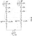
- the diplexer circuit assembly is shown in FIG. 44 and depicts three ports:
- the diplexer response is illustrated in FIG. 45 .
- the higher-harmonics rejection is below -40 dB, and the isolation between the lower and upper band is maintained below -40 dB.
- the isolation between transceiver ports 2 and 3 is maintained below -40dB.
Landscapes
- Physics & Mathematics (AREA)
- Electromagnetism (AREA)
- Control Of Motors That Do Not Use Commutators (AREA)
- Filters And Equalizers (AREA)
- Filtering Materials (AREA)
- Networks Using Active Elements (AREA)
Claims (12)
- Eine Filtervorrichtung, bestehend aus:-einer erweiterten, zusammengesetzten rechts- und linksliegenden (E-CRLH) Metamaterial-Einheit-Zellstruktur, gebildet aus einer nicht-linearen Kombination einer konventionellen CRLH Zelle und einer Dual-CRLH-Zelle;einer Kombination aus einem Serien-Induktor LR und einer Serien-kapazität CL der konventionellen CRLH Zelle, die eine Serien-Resonanz ωSE produziert,einer Kombination aus einem Shunt-Induktor LL und einer Shunt-Kapazität CR der konventionellen CRLH Zelle, die eine Shunt-Resonanz ωSH produziert,einer Kombination aus einem Serien-Induktor LR' und einer Kapazität CL' der Dual-CRLH Zelle, die eine Serien-Resonanz ωSE produziert, undeiner Kombination aus einem Shunt-Induktor LL' und einer Shunt-Kapazität CR' der Dual-CRLH Zelle, die eine Shunt-Resonanz ωSH produziert;wobei der Serien-Induktor LR, die Serien-Kapazität der Serie CL, der Shunt-Induktor LL, die Shunt-Kapazität CR, der Serien-Induktor LR' die, Serien- Kapazität CL', der Shunt-Induktor LL' und die Shunt-Kapazität CR' verbunden sind, um eine symmetrische Zellstruktur für die E-CRLH Elementarzelle zu bilden, wo ein Eingang und ein Ausgang der Elementarzelle E-CRLH eine gemeinsame Schaltungsstruktur haben; undwobei der Serien-Induktor LR, die Serien-Kapazität CL, der Shunt-Induktor LL, die Shunt-Kapazität CR, der Serien-Induktor LR', die Serien-Kapazität CL', der Shunt-Induktor LL' und die Shunt-Kapazität CR' solche Werte haben, dassωSE und ωSH im Wesentlichen gleich sind, undωSH und ωSE im Wesentlichen gleich sind; dadurch gekennzeichnet, dass
ωSE ≠ ωSHwobei die Filtervorrichtung über zwei Bandpass-Regionen verfügt, die durch eine Stop-Band-Region getrennt sind. - Vorrichtung nach Anspruch 1, bestehend aus einer oder mehr zusätzlichen E-CRLH Elementarzelle/n, die an die E-CRLH Elementarzelle gekoppelt ist/ sind.
- Vorrichtung nach Anspruch 1, bestehend aus einem Tiefpass-Filter, der an die E-CRLH Elementarzelle gekoppelt ist.
- Vorrichtung nach Anspruch 1, bestehend aus einem Tiefpass-Filter, der an die E-CRLH Elementarzelle gekoppelt ist.
- Vorrichtung nach Anspruch 1, wobei ein Verhältnis von LR/CR und ein Verhältnis von LL'/ CL' im Wesentlichen gleich sind.
- Vorrichtung nach Anspruch 1, wobei Werte der LR, CL, LL, CR, LR', CL', LL', CR' ausgewählt werden, um einer Eingangs-Impedanz und einer Ausgangs-Impedanz des Gerätes zugeordnet zu werden.
- Vorrichtung nach Anspruch 1, wobei der Serien-Induktor LR ausgewählt wird, um eine Eingangs-Impedanz und eine Ausgangs-Impedanz des Gerätes einander zuzuordnen.
- Vorrichtung nach Anspruch 1, wobei die E-CRLH Elementarzelle eine Leiterplattenstruktur in vier getrennten Metallisierung-Schichten gebildet hat, die parallel zueinander angeordnet sind, und folgendes umfassen:eine erste Metallisierungsschicht, die folgendes umfasst: einen erstes Signal-Anschluss, eine erste Zuleitung, gekoppelt an den ersten Signal-Anschluss, eine erste Startrampe, gekoppelt an die erste Zuleitung und einen ersten Zellen-Patch, der abgetrennt und an die erste Startrampe kapazitiv gekoppelt ist, einen zweiten Zellen-Patch, welcher vom ersten Zellen-Patch getrennt, doch mit ihm gekoppelt ist, um ein Signal vom ersten Zellen-Patch zu erhalten, eine zweite Startrampe, die vom zweiten Zellen-Patch getrennt und kapazitiv an ihn gekoppelt ist, eine zweite Zuleitung, die an die zweite Startrampe gekoppelt ist und einen zweiten Signal-Anschluss, der an die zweite Zuleitung gekoppelt ist;eine zweite Metallisierungsschicht, die so gestaltet ist, dass sie einen ersten leitfähigen Zellen-Patch unterhalb der ersten Metallisierungsschicht und zwischen den ersten und zweiten Zellen-Patches positioniert, umfasst;eine dritte Metallisierungsschicht, die so gestaltet ist, dass sie eine zweite leitfähige Zelle unterhalb des ersten leitfähigen Zellen-Patch in der zweiten Metallisierungsschicht umfasst;eine erste leitfähige Verbindung, die den ersten leitfähigen Zellen-Patch in der zweiten Metallisierungsschicht und den zweiten leitfähigen Zellen-Patch in der dritten Metallisierungsschicht verbindet;eine vierte Metallisierungsschicht, die eine Masselektrode für die Vorrichtung bereitstellen;eine erste Zellenverbindung, die den ersten Zellen-Patch auf der Metallisierungsschicht mit der Masseelektrode in der vierten Metallisierungsschicht verbindet, wobei die erste Zelle vom ersten und zweiten leitfähigen Zellen-Patch getrennt sind und keinen direkten Kontakt mit ihnen haben; undeine zweite Zellenverbindung, die den zweiten Zellen-Patch auf der ersten Metallisierungsschicht mit der Masseelektrode in der vierten Metallisierungsschicht verbindet, wobei die zweite Zelle vom ersten und zweiten Zellen-Patch getrennt ist und keinen direkten Kontakt mit ihnen hat.
- Vorrichtung nach Anspruch 8, wobei:die erste Metallisierungsschicht so gestaltet ist, dass sie eine erste Top-Masseelektrode neben der ersten Startrampe und eine zweite, an die zweite Startrampe angrenzende Top-Masseelektrode umfasst;die zweite Metallisierungsschicht so gestaltet ist, dass sie eine erste untere Masseelektrode unterhalb der ersten Top-Masseelektrode und eine zweite untere Masseelektrode unterhalb der zweiten Top-Masseelektrode umfasst,die erste Top-Masseelektrode so gestaltet ist, dass sie zusammen mit der ersten unteren Masseelektrode einen ersten koplanaren Wellenleiter (CPW) unterstützen, welcher zwischen dem ersten Signal-Port und der ersten Zuleitung gekoppelt ist, unddie zweite obere Masseelektrode so gestaltet ist, dass sie zusammen mit der zweiten unteren Masseelektrode einen zweiten koplanaren Wellenleiter (CPW) unterstützt, der zwischen dem zweiten Signal-Port und der zweiten Zuleitung gekoppelt ist.
- Vorrichtung nach Anspruch 1, wobei die Schaltungslemente in der E-CRLH Elementarzelle diskrete Schaltungselemente umfassen.
- Vorrichtung nach Anspruch 1, wobei
die E-CLRH Elementarzelle so strukturiert ist, dass sie die Funktion eines Tiefpass-Filters auf einem niedrigen Frequenzbereich und eines Hochpass-Filters im oberen Frequenzbereich ausübt, und eine Isolierung zwischen dem oberen Rand des Tiefpass-Filters und einem unteren Rand des Hochpass-Filters gleich oder größer als 25dB ist. - Vorrichtung nach Anspruch 11, wobei der Tiefpass-Filter einen Frequenzbereich von 800-2170 MHz und der Hochpass-Filter einen Frequenzbereich von 2.3-6.0-GHz aufweist.
Applications Claiming Priority (3)
| Application Number | Priority Date | Filing Date | Title |
|---|---|---|---|
| US98876807P | 2007-11-16 | 2007-11-16 | |
| US5095408P | 2008-05-06 | 2008-05-06 | |
| PCT/US2008/012887 WO2009067197A2 (en) | 2007-11-16 | 2008-11-17 | Filter design methods and filters based on metamaterial structures |
Publications (3)
| Publication Number | Publication Date |
|---|---|
| EP2227859A2 EP2227859A2 (de) | 2010-09-15 |
| EP2227859A4 EP2227859A4 (de) | 2013-09-18 |
| EP2227859B1 true EP2227859B1 (de) | 2017-11-01 |
Family
ID=40668052
Family Applications (1)
| Application Number | Title | Priority Date | Filing Date |
|---|---|---|---|
| EP08851171.2A Active EP2227859B1 (de) | 2007-11-16 | 2008-11-17 | Filterdesignverfahren und filter auf der basis von metamaterialstrukturen |
Country Status (6)
| Country | Link |
|---|---|
| US (1) | US8237519B2 (de) |
| EP (1) | EP2227859B1 (de) |
| JP (1) | JP5662801B2 (de) |
| KR (1) | KR101192231B1 (de) |
| CN (1) | CN102017404B (de) |
| WO (1) | WO2009067197A2 (de) |
Families Citing this family (47)
| Publication number | Priority date | Publication date | Assignee | Title |
|---|---|---|---|---|
| EP2227859B1 (de) | 2007-11-16 | 2017-11-01 | Gula Consulting Limited Liability Company | Filterdesignverfahren und filter auf der basis von metamaterialstrukturen |
| EP2279566A4 (de) * | 2008-05-06 | 2015-01-21 | Hollinworth Fund L L C | Einzelkabelantennenmodul für laptop und mobile geräte |
| WO2010075190A2 (en) * | 2008-12-24 | 2010-07-01 | Rayspan Corporation | Rf front-end module and antenna systems |
| KR101179421B1 (ko) * | 2009-02-18 | 2012-09-05 | 레이스팬 코포레이션 | 메타 재료 전력 증폭기 시스템 |
| KR101072591B1 (ko) * | 2009-08-10 | 2011-10-11 | 삼성전기주식회사 | Emi 노이즈 저감 인쇄회로기판 |
| US8334734B2 (en) * | 2009-08-25 | 2012-12-18 | Hollinworth Fund, L.L.C. | Printed multilayer filter methods and designs using extended CRLH (E-CRLH) |
| KR101021548B1 (ko) * | 2009-09-18 | 2011-03-16 | 삼성전기주식회사 | 전자기 밴드갭 구조를 구비하는 인쇄회로기판 |
| KR101021551B1 (ko) * | 2009-09-22 | 2011-03-16 | 삼성전기주식회사 | 전자기 밴드갭 구조를 구비하는 인쇄회로기판 |
| US8141784B2 (en) | 2009-09-25 | 2012-03-27 | Hand Held Products, Inc. | Encoded information reading terminal with user-configurable multi-protocol wireless communication interface |
| US9543661B2 (en) * | 2009-11-09 | 2017-01-10 | Tyco Electronics Services Gmbh | RF module and antenna systems |
| US20110116424A1 (en) * | 2009-11-19 | 2011-05-19 | Hand Held Products, Inc. | Network-agnostic encoded information reading terminal |
| US8576024B2 (en) * | 2010-02-11 | 2013-11-05 | Hollinworth Fund, L.L.C. | Electro-acoustic filter |
| US8680945B1 (en) * | 2010-02-17 | 2014-03-25 | Lockheed Martin Corporation | Metamaterial enabled compact wideband tunable phase shifters |
| KR101321772B1 (ko) * | 2010-03-31 | 2013-10-28 | 한국전자통신연구원 | 통신 시스템에서 공진기 및 그를 이용한 필터 |
| KR20110113340A (ko) * | 2010-04-09 | 2011-10-17 | 한국전자통신연구원 | Crlh 구조 공진기 기반의 대역 통과 필터 및 이를 이용한 듀플렉서 |
| WO2013016921A1 (zh) * | 2011-07-29 | 2013-02-07 | 深圳光启高等理工研究院 | 一种谐振腔及具有该谐振腔的滤波器 |
| US8596533B2 (en) | 2011-08-17 | 2013-12-03 | Hand Held Products, Inc. | RFID devices using metamaterial antennas |
| US10013588B2 (en) | 2011-08-17 | 2018-07-03 | Hand Held Products, Inc. | Encoded information reading terminal with multi-directional antenna |
| US8779898B2 (en) | 2011-08-17 | 2014-07-15 | Hand Held Products, Inc. | Encoded information reading terminal with micro-electromechanical radio frequency front end |
| CN102956950B (zh) * | 2011-08-31 | 2015-05-27 | 深圳光启高等理工研究院 | 基于超材料的定向耦合器 |
| KR101252687B1 (ko) * | 2012-02-21 | 2013-04-09 | 주식회사 이너트론 | 메타매질을 이용한 저역 통과 필터 |
| CN103293684B (zh) * | 2012-02-29 | 2017-03-29 | 深圳光启智能光子技术有限公司 | 3d显示装置 |
| TWI549353B (zh) | 2013-01-14 | 2016-09-11 | 宏碁股份有限公司 | 行動裝置 |
| EP2974000B1 (de) * | 2013-03-15 | 2024-07-17 | Dockon AG | Frequenzselektiver logarithmischer verstärker mit intrinsischer frequenzdemodulationsfähigkeit |
| US8999992B2 (en) | 2013-03-15 | 2015-04-07 | Vm Pharma Llc | Crystalline forms of tryosine kinase inhibitors and their salts |
| KR101451360B1 (ko) * | 2013-08-30 | 2014-10-15 | 금오공과대학교 산학협력단 | 병렬 구조 crlh 전송선로를 이용한 광대역 필터 |
| GB2517987A (en) | 2013-09-09 | 2015-03-11 | Isis Innovation | Waveguide |
| US11082014B2 (en) | 2013-09-12 | 2021-08-03 | Dockon Ag | Advanced amplifier system for ultra-wide band RF communication |
| US11183974B2 (en) | 2013-09-12 | 2021-11-23 | Dockon Ag | Logarithmic detector amplifier system in open-loop configuration for use as high sensitivity selective receiver without frequency conversion |
| EP3044723A4 (de) | 2013-09-12 | 2017-05-03 | Dockon AG | Logarithmisches detektorverstärkersystem zur verwendung als hochempfindlicher selektiver empfänger ohne frequenzumsetzung |
| US9424994B2 (en) | 2013-12-10 | 2016-08-23 | Tdk Corporation | Tunable interdigitated capacitor |
| US9443657B1 (en) | 2013-12-10 | 2016-09-13 | Tdk Corporation | Piezo controlled variable capacitor |
| US9474150B2 (en) | 2013-12-10 | 2016-10-18 | Tdk Corporation | Transmission line filter with tunable capacitor |
| CN104934718A (zh) * | 2014-03-18 | 2015-09-23 | 深圳光启创新技术有限公司 | 高通滤波超材料、天线罩和天线系统 |
| US10301271B2 (en) | 2014-09-17 | 2019-05-28 | Purdue Pharma L.P. | Crystalline forms of tyrosine kinase inhibitors and their salts |
| KR101944652B1 (ko) * | 2015-01-23 | 2019-01-31 | 가부시키가이샤 무라타 세이사쿠쇼 | 필터 장치 |
| DE102015201773A1 (de) * | 2015-02-02 | 2016-08-04 | Ihp Gmbh-Innovations For High Performance Microelectronics / Leibniz-Institut Für Innovative Mikroelektronik | Inhomogene Übertragungsleitung zur positionsaufgelösten Permittivitätsbestimmung |
| CN104617907B (zh) * | 2015-03-02 | 2018-08-10 | 联想(北京)有限公司 | 一种双工器及电子设备 |
| US10542622B2 (en) * | 2016-07-27 | 2020-01-21 | National University Corporation Okayama University | Printed wiring board |
| JP6611065B2 (ja) * | 2016-07-27 | 2019-11-27 | 国立大学法人 岡山大学 | 印刷配線板 |
| CN107888158A (zh) * | 2017-11-07 | 2018-04-06 | 福建北峰通信科技股份有限公司 | 一种电调谐射频带通滤波器电路 |
| JP6998594B2 (ja) * | 2018-03-05 | 2022-02-04 | 国立大学法人京都工芸繊維大学 | 非相反伝送線路装置及びアンテナ装置 |
| CN111525903B (zh) * | 2020-03-30 | 2022-02-08 | 北京邮电大学 | 一种基于薄膜ipd技术的宽频带吸收式带阻滤波器芯片 |
| CN113872552B (zh) * | 2021-10-08 | 2024-07-02 | 南京国博电子股份有限公司 | 一种四阶滤波响应的多模集总式滤波器 |
| JP2023121294A (ja) * | 2022-02-21 | 2023-08-31 | Tdk株式会社 | フィルタ |
| CN115377636B (zh) * | 2022-08-19 | 2023-12-15 | 苏州立讯技术有限公司 | 滤波器及其制造方法 |
| CN117081542A (zh) * | 2023-10-17 | 2023-11-17 | 中科海高(成都)电子技术有限公司 | 滤波器组 |
Family Cites Families (22)
| Publication number | Priority date | Publication date | Assignee | Title |
|---|---|---|---|---|
| US6686886B2 (en) * | 2001-05-29 | 2004-02-03 | International Business Machines Corporation | Integrated antenna for laptop applications |
| KR100451188B1 (ko) * | 2002-03-19 | 2004-10-02 | 엘지전자 주식회사 | 이동통신단말기의 수신장치 |
| US6859114B2 (en) * | 2002-05-31 | 2005-02-22 | George V. Eleftheriades | Metamaterials for controlling and guiding electromagnetic radiation and applications therefor |
| US6794952B2 (en) * | 2002-06-27 | 2004-09-21 | Harris Corporation | High efficiency low pass filter |
| US6781486B2 (en) * | 2002-06-27 | 2004-08-24 | Harris Corporation | High efficiency stepped impedance filter |
| JPWO2004073108A1 (ja) * | 2003-02-14 | 2006-06-01 | 株式会社東芝 | 電子機器 |
| JP4095501B2 (ja) * | 2003-06-25 | 2008-06-04 | インターナショナル・ビジネス・マシーンズ・コーポレーション | コンピュータ装置、無線アクセスポイント、無線ネットワークを介した電源投入方法、フレーム聴取方法、フレーム送信方法、およびプログラム |
| KR20050011047A (ko) | 2003-07-21 | 2005-01-29 | 주식회사 팬택앤큐리텔 | 트라이 밴드용 이동통신 단말기의 송수신 장치 |
| US7508283B2 (en) * | 2004-03-26 | 2009-03-24 | The Regents Of The University Of California | Composite right/left handed (CRLH) couplers |
| US7330090B2 (en) * | 2004-03-26 | 2008-02-12 | The Regents Of The University Of California | Zeroeth-order resonator |
| US7012484B2 (en) * | 2004-04-26 | 2006-03-14 | Integrated System Solution Corp. | Filter using multilayer ceramic technology and structure thereof |
| WO2006137575A1 (ja) * | 2005-06-24 | 2006-12-28 | National University Corporation Yamaguchi University | ストリップ線路型の右手/左手系複合線路または左手系線路とそれらを用いたアンテナ |
| US7446712B2 (en) * | 2005-12-21 | 2008-11-04 | The Regents Of The University Of California | Composite right/left-handed transmission line based compact resonant antenna for RF module integration |
| JP4629571B2 (ja) * | 2005-12-26 | 2011-02-09 | 三菱電機株式会社 | マイクロ波回路 |
| CN103441339B (zh) * | 2006-04-27 | 2016-01-13 | 泰科电子服务有限责任公司 | 异向材料天线设备 |
| US7482893B2 (en) * | 2006-05-18 | 2009-01-27 | The Regents Of The University Of California | Power combiners using meta-material composite right/left hand transmission line at infinite wavelength frequency |
| US7741933B2 (en) * | 2006-06-30 | 2010-06-22 | The Charles Stark Draper Laboratory, Inc. | Electromagnetic composite metamaterial |
| TWI449257B (zh) * | 2006-08-25 | 2014-08-11 | Tyco Electronics Services Gmbh | 寬頻和緊實多頻超穎材料結構以及天線 |
| US7952526B2 (en) * | 2006-08-30 | 2011-05-31 | The Regents Of The University Of California | Compact dual-band resonator using anisotropic metamaterial |
| EP2227859B1 (de) | 2007-11-16 | 2017-11-01 | Gula Consulting Limited Liability Company | Filterdesignverfahren und filter auf der basis von metamaterialstrukturen |
| EP2279566A4 (de) | 2008-05-06 | 2015-01-21 | Hollinworth Fund L L C | Einzelkabelantennenmodul für laptop und mobile geräte |
| US8334734B2 (en) * | 2009-08-25 | 2012-12-18 | Hollinworth Fund, L.L.C. | Printed multilayer filter methods and designs using extended CRLH (E-CRLH) |
-
2008
- 2008-11-17 EP EP08851171.2A patent/EP2227859B1/de active Active
- 2008-11-17 WO PCT/US2008/012887 patent/WO2009067197A2/en not_active Ceased
- 2008-11-17 US US12/272,781 patent/US8237519B2/en active Active
- 2008-11-17 KR KR1020107013297A patent/KR101192231B1/ko active Active
- 2008-11-17 CN CN2008801249315A patent/CN102017404B/zh active Active
- 2008-11-17 JP JP2010534057A patent/JP5662801B2/ja active Active
Non-Patent Citations (1)
| Title |
|---|
| None * |
Also Published As
| Publication number | Publication date |
|---|---|
| CN102017404B (zh) | 2013-11-20 |
| EP2227859A4 (de) | 2013-09-18 |
| US20090160578A1 (en) | 2009-06-25 |
| CN102017404A (zh) | 2011-04-13 |
| US20100109805A2 (en) | 2010-05-06 |
| JP2011508468A (ja) | 2011-03-10 |
| US8237519B2 (en) | 2012-08-07 |
| JP5662801B2 (ja) | 2015-02-04 |
| WO2009067197A2 (en) | 2009-05-28 |
| WO2009067197A3 (en) | 2009-09-11 |
| KR20100099702A (ko) | 2010-09-13 |
| EP2227859A2 (de) | 2010-09-15 |
| KR101192231B1 (ko) | 2012-10-17 |
Similar Documents
| Publication | Publication Date | Title |
|---|---|---|
| EP2227859B1 (de) | Filterdesignverfahren und filter auf der basis von metamaterialstrukturen | |
| US8334734B2 (en) | Printed multilayer filter methods and designs using extended CRLH (E-CRLH) | |
| EP2201645B1 (de) | Einschichtmetallisierung und lochfreie metamaterialstrukturen | |
| EP2070157B1 (de) | Antennen auf der basis von metamaterialstrukturen | |
| KR101226060B1 (ko) | 단일피드 다중셀 메타물질 안테나 기기 | |
| US8294533B2 (en) | Power combiners and dividers based on composite right and left handed metamaterial structures | |
| US20100109971A2 (en) | Metamaterial structures with multilayer metallization and via | |
| EP2279566A2 (de) | Einzelkabelantennenmodul für laptop und mobile geräte | |
| CN102403562A (zh) | 集成了双频带通滤波器的功率分配器 | |
| US9184481B2 (en) | Power combiners and dividers based on composite right and left handed metamaterial structures | |
| Al-Naib et al. | Single metal layer CPW metamaterial bandpass filter |
Legal Events
| Date | Code | Title | Description |
|---|---|---|---|
| PUAI | Public reference made under article 153(3) epc to a published international application that has entered the european phase |
Free format text: ORIGINAL CODE: 0009012 |
|
| 17P | Request for examination filed |
Effective date: 20100616 |
|
| AK | Designated contracting states |
Kind code of ref document: A2 Designated state(s): AT BE BG CH CY CZ DE DK EE ES FI FR GB GR HR HU IE IS IT LI LT LU LV MC MT NL NO PL PT RO SE SI SK TR |
|
| AX | Request for extension of the european patent |
Extension state: AL BA MK RS |
|
| DAX | Request for extension of the european patent (deleted) | ||
| RAP1 | Party data changed (applicant data changed or rights of an application transferred) |
Owner name: HOLLINWORTH FUND , L.L.C. |
|
| REG | Reference to a national code |
Ref country code: DE Ref legal event code: R079 Ref document number: 602008052805 Country of ref document: DE Free format text: PREVIOUS MAIN CLASS: H03H0007000000 Ipc: H03H0007010000 |
|
| A4 | Supplementary search report drawn up and despatched |
Effective date: 20130816 |
|
| RIC1 | Information provided on ipc code assigned before grant |
Ipc: H01P 3/08 20060101ALI20130809BHEP Ipc: H03H 7/01 20060101AFI20130809BHEP Ipc: H01P 1/213 20060101ALI20130809BHEP Ipc: H01P 1/203 20060101ALI20130809BHEP |
|
| 17Q | First examination report despatched |
Effective date: 20160219 |
|
| GRAP | Despatch of communication of intention to grant a patent |
Free format text: ORIGINAL CODE: EPIDOSNIGR1 |
|
| INTG | Intention to grant announced |
Effective date: 20170412 |
|
| GRAS | Grant fee paid |
Free format text: ORIGINAL CODE: EPIDOSNIGR3 |
|
| GRAA | (expected) grant |
Free format text: ORIGINAL CODE: 0009210 |
|
| RAP1 | Party data changed (applicant data changed or rights of an application transferred) |
Owner name: GULA CONSULTING LIMITED LIABILITY COMPANY |
|
| GRAT | Correction requested after decision to grant or after decision to maintain patent in amended form |
Free format text: ORIGINAL CODE: EPIDOSNCDEC |
|
| AK | Designated contracting states |
Kind code of ref document: B1 Designated state(s): AT BE BG CH CY CZ DE DK EE ES FI FR GB GR HR HU IE IS IT LI LT LU LV MC MT NL NO PL PT RO SE SI SK TR |
|
| REG | Reference to a national code |
Ref country code: GB Ref legal event code: FG4D |
|
| REG | Reference to a national code |
Ref country code: CH Ref legal event code: EP Ref country code: AT Ref legal event code: REF Ref document number: 942984 Country of ref document: AT Kind code of ref document: T Effective date: 20171115 |
|
| REG | Reference to a national code |
Ref country code: FR Ref legal event code: PLFP Year of fee payment: 10 |
|
| REG | Reference to a national code |
Ref country code: IE Ref legal event code: FG4D |
|
| REG | Reference to a national code |
Ref country code: DE Ref legal event code: R096 Ref document number: 602008052805 Country of ref document: DE |
|
| REG | Reference to a national code |
Ref country code: NL Ref legal event code: MP Effective date: 20171101 |
|
| REG | Reference to a national code |
Ref country code: LT Ref legal event code: MG4D |
|
| REG | Reference to a national code |
Ref country code: AT Ref legal event code: MK05 Ref document number: 942984 Country of ref document: AT Kind code of ref document: T Effective date: 20171101 |
|
| PG25 | Lapsed in a contracting state [announced via postgrant information from national office to epo] |
Ref country code: NO Free format text: LAPSE BECAUSE OF FAILURE TO SUBMIT A TRANSLATION OF THE DESCRIPTION OR TO PAY THE FEE WITHIN THE PRESCRIBED TIME-LIMIT Effective date: 20180201 Ref country code: NL Free format text: LAPSE BECAUSE OF FAILURE TO SUBMIT A TRANSLATION OF THE DESCRIPTION OR TO PAY THE FEE WITHIN THE PRESCRIBED TIME-LIMIT Effective date: 20171101 Ref country code: LT Free format text: LAPSE BECAUSE OF FAILURE TO SUBMIT A TRANSLATION OF THE DESCRIPTION OR TO PAY THE FEE WITHIN THE PRESCRIBED TIME-LIMIT Effective date: 20171101 Ref country code: ES Free format text: LAPSE BECAUSE OF FAILURE TO SUBMIT A TRANSLATION OF THE DESCRIPTION OR TO PAY THE FEE WITHIN THE PRESCRIBED TIME-LIMIT Effective date: 20171101 Ref country code: SE Free format text: LAPSE BECAUSE OF FAILURE TO SUBMIT A TRANSLATION OF THE DESCRIPTION OR TO PAY THE FEE WITHIN THE PRESCRIBED TIME-LIMIT Effective date: 20171101 Ref country code: FI Free format text: LAPSE BECAUSE OF FAILURE TO SUBMIT A TRANSLATION OF THE DESCRIPTION OR TO PAY THE FEE WITHIN THE PRESCRIBED TIME-LIMIT Effective date: 20171101 |
|
| PG25 | Lapsed in a contracting state [announced via postgrant information from national office to epo] |
Ref country code: BG Free format text: LAPSE BECAUSE OF FAILURE TO SUBMIT A TRANSLATION OF THE DESCRIPTION OR TO PAY THE FEE WITHIN THE PRESCRIBED TIME-LIMIT Effective date: 20180201 Ref country code: GR Free format text: LAPSE BECAUSE OF FAILURE TO SUBMIT A TRANSLATION OF THE DESCRIPTION OR TO PAY THE FEE WITHIN THE PRESCRIBED TIME-LIMIT Effective date: 20180202 Ref country code: HR Free format text: LAPSE BECAUSE OF FAILURE TO SUBMIT A TRANSLATION OF THE DESCRIPTION OR TO PAY THE FEE WITHIN THE PRESCRIBED TIME-LIMIT Effective date: 20171101 Ref country code: AT Free format text: LAPSE BECAUSE OF FAILURE TO SUBMIT A TRANSLATION OF THE DESCRIPTION OR TO PAY THE FEE WITHIN THE PRESCRIBED TIME-LIMIT Effective date: 20171101 Ref country code: IS Free format text: LAPSE BECAUSE OF FAILURE TO SUBMIT A TRANSLATION OF THE DESCRIPTION OR TO PAY THE FEE WITHIN THE PRESCRIBED TIME-LIMIT Effective date: 20180301 Ref country code: LV Free format text: LAPSE BECAUSE OF FAILURE TO SUBMIT A TRANSLATION OF THE DESCRIPTION OR TO PAY THE FEE WITHIN THE PRESCRIBED TIME-LIMIT Effective date: 20171101 |
|
| PG25 | Lapsed in a contracting state [announced via postgrant information from national office to epo] |
Ref country code: LI Free format text: LAPSE BECAUSE OF NON-PAYMENT OF DUE FEES Effective date: 20171130 Ref country code: SK Free format text: LAPSE BECAUSE OF FAILURE TO SUBMIT A TRANSLATION OF THE DESCRIPTION OR TO PAY THE FEE WITHIN THE PRESCRIBED TIME-LIMIT Effective date: 20171101 Ref country code: DK Free format text: LAPSE BECAUSE OF FAILURE TO SUBMIT A TRANSLATION OF THE DESCRIPTION OR TO PAY THE FEE WITHIN THE PRESCRIBED TIME-LIMIT Effective date: 20171101 Ref country code: CY Free format text: LAPSE BECAUSE OF FAILURE TO SUBMIT A TRANSLATION OF THE DESCRIPTION OR TO PAY THE FEE WITHIN THE PRESCRIBED TIME-LIMIT Effective date: 20171101 Ref country code: EE Free format text: LAPSE BECAUSE OF FAILURE TO SUBMIT A TRANSLATION OF THE DESCRIPTION OR TO PAY THE FEE WITHIN THE PRESCRIBED TIME-LIMIT Effective date: 20171101 Ref country code: CH Free format text: LAPSE BECAUSE OF NON-PAYMENT OF DUE FEES Effective date: 20171130 Ref country code: CZ Free format text: LAPSE BECAUSE OF FAILURE TO SUBMIT A TRANSLATION OF THE DESCRIPTION OR TO PAY THE FEE WITHIN THE PRESCRIBED TIME-LIMIT Effective date: 20171101 |
|
| REG | Reference to a national code |
Ref country code: DE Ref legal event code: R097 Ref document number: 602008052805 Country of ref document: DE |
|
| PG25 | Lapsed in a contracting state [announced via postgrant information from national office to epo] |
Ref country code: RO Free format text: LAPSE BECAUSE OF FAILURE TO SUBMIT A TRANSLATION OF THE DESCRIPTION OR TO PAY THE FEE WITHIN THE PRESCRIBED TIME-LIMIT Effective date: 20171101 Ref country code: IT Free format text: LAPSE BECAUSE OF FAILURE TO SUBMIT A TRANSLATION OF THE DESCRIPTION OR TO PAY THE FEE WITHIN THE PRESCRIBED TIME-LIMIT Effective date: 20171101 Ref country code: LU Free format text: LAPSE BECAUSE OF NON-PAYMENT OF DUE FEES Effective date: 20171117 Ref country code: PL Free format text: LAPSE BECAUSE OF FAILURE TO SUBMIT A TRANSLATION OF THE DESCRIPTION OR TO PAY THE FEE WITHIN THE PRESCRIBED TIME-LIMIT Effective date: 20171101 |
|
| REG | Reference to a national code |
Ref country code: BE Ref legal event code: MM Effective date: 20171130 |
|
| REG | Reference to a national code |
Ref country code: IE Ref legal event code: MM4A |
|
| PLBE | No opposition filed within time limit |
Free format text: ORIGINAL CODE: 0009261 |
|
| STAA | Information on the status of an ep patent application or granted ep patent |
Free format text: STATUS: NO OPPOSITION FILED WITHIN TIME LIMIT |
|
| PG25 | Lapsed in a contracting state [announced via postgrant information from national office to epo] |
Ref country code: MT Free format text: LAPSE BECAUSE OF NON-PAYMENT OF DUE FEES Effective date: 20171117 |
|
| 26N | No opposition filed |
Effective date: 20180802 |
|
| REG | Reference to a national code |
Ref country code: FR Ref legal event code: PLFP Year of fee payment: 11 |
|
| PG25 | Lapsed in a contracting state [announced via postgrant information from national office to epo] |
Ref country code: IE Free format text: LAPSE BECAUSE OF NON-PAYMENT OF DUE FEES Effective date: 20171117 |
|
| PG25 | Lapsed in a contracting state [announced via postgrant information from national office to epo] |
Ref country code: SI Free format text: LAPSE BECAUSE OF FAILURE TO SUBMIT A TRANSLATION OF THE DESCRIPTION OR TO PAY THE FEE WITHIN THE PRESCRIBED TIME-LIMIT Effective date: 20171101 Ref country code: BE Free format text: LAPSE BECAUSE OF NON-PAYMENT OF DUE FEES Effective date: 20171130 |
|
| PG25 | Lapsed in a contracting state [announced via postgrant information from national office to epo] |
Ref country code: HU Free format text: LAPSE BECAUSE OF FAILURE TO SUBMIT A TRANSLATION OF THE DESCRIPTION OR TO PAY THE FEE WITHIN THE PRESCRIBED TIME-LIMIT; INVALID AB INITIO Effective date: 20081117 Ref country code: MC Free format text: LAPSE BECAUSE OF FAILURE TO SUBMIT A TRANSLATION OF THE DESCRIPTION OR TO PAY THE FEE WITHIN THE PRESCRIBED TIME-LIMIT Effective date: 20171101 |
|
| PG25 | Lapsed in a contracting state [announced via postgrant information from national office to epo] |
Ref country code: TR Free format text: LAPSE BECAUSE OF FAILURE TO SUBMIT A TRANSLATION OF THE DESCRIPTION OR TO PAY THE FEE WITHIN THE PRESCRIBED TIME-LIMIT Effective date: 20171101 |
|
| PG25 | Lapsed in a contracting state [announced via postgrant information from national office to epo] |
Ref country code: PT Free format text: LAPSE BECAUSE OF FAILURE TO SUBMIT A TRANSLATION OF THE DESCRIPTION OR TO PAY THE FEE WITHIN THE PRESCRIBED TIME-LIMIT Effective date: 20171101 |
|
| P01 | Opt-out of the competence of the unified patent court (upc) registered |
Effective date: 20230522 |
|
| PGFP | Annual fee paid to national office [announced via postgrant information from national office to epo] |
Ref country code: DE Payment date: 20251013 Year of fee payment: 18 |
|
| PGFP | Annual fee paid to national office [announced via postgrant information from national office to epo] |
Ref country code: GB Payment date: 20251009 Year of fee payment: 18 |
|
| PGFP | Annual fee paid to national office [announced via postgrant information from national office to epo] |
Ref country code: FR Payment date: 20251013 Year of fee payment: 18 |