EP2227824B1 - Memory cell that employs a selectively fabricated carbon nano-tube reversible resistance-switching element and methods of forming the same - Google Patents
Memory cell that employs a selectively fabricated carbon nano-tube reversible resistance-switching element and methods of forming the same Download PDFInfo
- Publication number
- EP2227824B1 EP2227824B1 EP08869555.6A EP08869555A EP2227824B1 EP 2227824 B1 EP2227824 B1 EP 2227824B1 EP 08869555 A EP08869555 A EP 08869555A EP 2227824 B1 EP2227824 B1 EP 2227824B1
- Authority
- EP
- European Patent Office
- Prior art keywords
- layer
- cnt
- memory cell
- memory
- switching element
- Prior art date
- Legal status (The legal status is an assumption and is not a legal conclusion. Google has not performed a legal analysis and makes no representation as to the accuracy of the status listed.)
- Not-in-force
Links
Images


Classifications
-
- G—PHYSICS
- G11—INFORMATION STORAGE
- G11C—STATIC STORES
- G11C13/00—Digital stores characterised by the use of storage elements not covered by groups G11C11/00, G11C23/00, or G11C25/00
- G11C13/02—Digital stores characterised by the use of storage elements not covered by groups G11C11/00, G11C23/00, or G11C25/00 using elements whose operation depends upon chemical change
- G11C13/025—Digital stores characterised by the use of storage elements not covered by groups G11C11/00, G11C23/00, or G11C25/00 using elements whose operation depends upon chemical change using fullerenes, e.g. C60, or nanotubes, e.g. carbon or silicon nanotubes
-
- H—ELECTRICITY
- H10—SEMICONDUCTOR DEVICES; ELECTRIC SOLID-STATE DEVICES NOT OTHERWISE PROVIDED FOR
- H10N—ELECTRIC SOLID-STATE DEVICES NOT OTHERWISE PROVIDED FOR
- H10N70/00—Solid-state devices having no potential barriers, and specially adapted for rectifying, amplifying, oscillating or switching
- H10N70/20—Multistable switching devices, e.g. memristors
-
- B—PERFORMING OPERATIONS; TRANSPORTING
- B82—NANOTECHNOLOGY
- B82Y—SPECIFIC USES OR APPLICATIONS OF NANOSTRUCTURES; MEASUREMENT OR ANALYSIS OF NANOSTRUCTURES; MANUFACTURE OR TREATMENT OF NANOSTRUCTURES
- B82Y10/00—Nanotechnology for information processing, storage or transmission, e.g. quantum computing or single electron logic
-
- G—PHYSICS
- G11—INFORMATION STORAGE
- G11C—STATIC STORES
- G11C13/00—Digital stores characterised by the use of storage elements not covered by groups G11C11/00, G11C23/00, or G11C25/00
- G11C13/0002—Digital stores characterised by the use of storage elements not covered by groups G11C11/00, G11C23/00, or G11C25/00 using resistive RAM [RRAM] elements
- G11C13/0004—Digital stores characterised by the use of storage elements not covered by groups G11C11/00, G11C23/00, or G11C25/00 using resistive RAM [RRAM] elements comprising amorphous/crystalline phase transition cells
-
- G—PHYSICS
- G11—INFORMATION STORAGE
- G11C—STATIC STORES
- G11C5/00—Details of stores covered by group G11C11/00
- G11C5/02—Disposition of storage elements, e.g. in the form of a matrix array
-
- H—ELECTRICITY
- H10—SEMICONDUCTOR DEVICES; ELECTRIC SOLID-STATE DEVICES NOT OTHERWISE PROVIDED FOR
- H10B—ELECTRONIC MEMORY DEVICES
- H10B63/00—Resistance change memory devices, e.g. resistive RAM [ReRAM] devices
- H10B63/20—Resistance change memory devices, e.g. resistive RAM [ReRAM] devices comprising selection components having two electrodes, e.g. diodes
-
- H—ELECTRICITY
- H10—SEMICONDUCTOR DEVICES; ELECTRIC SOLID-STATE DEVICES NOT OTHERWISE PROVIDED FOR
- H10B—ELECTRONIC MEMORY DEVICES
- H10B63/00—Resistance change memory devices, e.g. resistive RAM [ReRAM] devices
- H10B63/30—Resistance change memory devices, e.g. resistive RAM [ReRAM] devices comprising selection components having three or more electrodes, e.g. transistors
-
- H—ELECTRICITY
- H10—SEMICONDUCTOR DEVICES; ELECTRIC SOLID-STATE DEVICES NOT OTHERWISE PROVIDED FOR
- H10B—ELECTRONIC MEMORY DEVICES
- H10B63/00—Resistance change memory devices, e.g. resistive RAM [ReRAM] devices
- H10B63/80—Arrangements comprising multiple bistable or multi-stable switching components of the same type on a plane parallel to the substrate, e.g. cross-point arrays
- H10B63/84—Arrangements comprising multiple bistable or multi-stable switching components of the same type on a plane parallel to the substrate, e.g. cross-point arrays arranged in a direction perpendicular to the substrate, e.g. 3D cell arrays
-
- H—ELECTRICITY
- H10—SEMICONDUCTOR DEVICES; ELECTRIC SOLID-STATE DEVICES NOT OTHERWISE PROVIDED FOR
- H10N—ELECTRIC SOLID-STATE DEVICES NOT OTHERWISE PROVIDED FOR
- H10N70/00—Solid-state devices having no potential barriers, and specially adapted for rectifying, amplifying, oscillating or switching
- H10N70/011—Manufacture or treatment of multistable switching devices
- H10N70/021—Formation of switching materials, e.g. deposition of layers
- H10N70/023—Formation of switching materials, e.g. deposition of layers by chemical vapor deposition, e.g. MOCVD, ALD
-
- H—ELECTRICITY
- H10—SEMICONDUCTOR DEVICES; ELECTRIC SOLID-STATE DEVICES NOT OTHERWISE PROVIDED FOR
- H10N—ELECTRIC SOLID-STATE DEVICES NOT OTHERWISE PROVIDED FOR
- H10N70/00—Solid-state devices having no potential barriers, and specially adapted for rectifying, amplifying, oscillating or switching
- H10N70/801—Constructional details of multistable switching devices
- H10N70/821—Device geometry
- H10N70/826—Device geometry adapted for essentially vertical current flow, e.g. sandwich or pillar type devices
-
- H—ELECTRICITY
- H10—SEMICONDUCTOR DEVICES; ELECTRIC SOLID-STATE DEVICES NOT OTHERWISE PROVIDED FOR
- H10N—ELECTRIC SOLID-STATE DEVICES NOT OTHERWISE PROVIDED FOR
- H10N70/00—Solid-state devices having no potential barriers, and specially adapted for rectifying, amplifying, oscillating or switching
- H10N70/801—Constructional details of multistable switching devices
- H10N70/881—Switching materials
- H10N70/884—Switching materials based on at least one element of group IIIA, IVA or VA, e.g. elemental or compound semiconductors
- H10N70/8845—Carbon or carbides
-
- G—PHYSICS
- G11—INFORMATION STORAGE
- G11C—STATIC STORES
- G11C2213/00—Indexing scheme relating to G11C13/00 for features not covered by this group
- G11C2213/30—Resistive cell, memory material aspects
- G11C2213/35—Material including carbon, e.g. graphite, grapheme
-
- G—PHYSICS
- G11—INFORMATION STORAGE
- G11C—STATIC STORES
- G11C2213/00—Indexing scheme relating to G11C13/00 for features not covered by this group
- G11C2213/70—Resistive array aspects
- G11C2213/71—Three dimensional array
-
- G—PHYSICS
- G11—INFORMATION STORAGE
- G11C—STATIC STORES
- G11C2213/00—Indexing scheme relating to G11C13/00 for features not covered by this group
- G11C2213/70—Resistive array aspects
- G11C2213/72—Array wherein the access device being a diode
-
- G—PHYSICS
- G11—INFORMATION STORAGE
- G11C—STATIC STORES
- G11C2213/00—Indexing scheme relating to G11C13/00 for features not covered by this group
- G11C2213/70—Resistive array aspects
- G11C2213/79—Array wherein the access device being a transistor
Definitions
- the present invention relates to non-volatile memories and more particularly to a memory cell that employs a selectively fabricated carbon nano-tube (CNT) reversible resistance-switching element and methods of forming the same.
- CNT carbon nano-tube
- Non-volatile memories formed from reversible resistance-switching elements are known.
- U.S. Patent Application Serial No. 11/125,939 filed May 9, 2005 and titled “REWRITABLE MEMORY CELL COMPRISING A DIODE AND A RESISTANCE-SWITCHING MATERIAL" (hereinafter "the ⁇ 939 Application”) (published as US 2006/2500836 ) describes a rewriteable non-volatile memory cell that includes a diode coupled in series with a reversible resistivity-switching material such as a metal oxide or metal nitride.
- US 2007/0158697 discloses a memory cell according to the precharacterising portion of claim 1.
- a memory cell comprising a reversible resistance-switching element coupled to a steering element.
- the reversible resistance-switching element comprises CNT material formed only on a CNT seeding layer comprising titanium nitride that has a surface roughness that supports formation of CNT material.
- the selectively formed CNT material is adapted to serve as the reversible resistance-switching element.
- a Method of fabricating a memory cell may include (1) fabricating a steering element above a substrate; and (2) fabricating a reversible-resistance switching element coupled to the steering element by selectively fabricating carbon nano-tube (CNT) material above the substrate.
- CNT carbon nano-tube
- Another method of fabricating a memory cell may include (1) fabricating a first conductor above a substrate; (2) fabricating a reversible-resistance switching element above the first conductor by selectively fabricating carbon nano-tube (CNT) material above the first conductor; (3) fabricating a diode above the first conductor; and (4) fabricating a second conductor above the diode and the reversible resistance-switching element.
- CNT carbon nano-tube
- a method of fabricating a memory cell that includes (1) fabricating a first conductor above a substrate; (2) fabricating a vertical polycrystalline diode above the first conductor; (3) fabricating a reversible-resistance switching element above the vertical polycrystalline diode by selectively fabricating carbon nano-tube (CNT) material above the vertical polycrystalline diode; and (4) fabricating a second conductor above the reversible-resistance switching element.
- CNT carbon nano-tube
- Another method of fabricating a memory cell may include (1) fabricating a thin film transistor having a source region and a drain region; (2) fabricating a first conductor coupled to the source region or the drain region of the transistor; (3) fabricating a reversible-resistance switching element coupled to the first conductor by selectively fabricating carbon nano-tube (CNT) material above the first conductor; and (4) fabricating a second conductor above the reversible resistance-switching element.
- CNT carbon nano-tube
- a memory cell that includes (1) a steering element; and (2) a reversible resistance-switching element coupled to the steering element and including selectively fabricated carbon nano-tube (CNT) material.
- CNT carbon nano-tube
- a memory cell that includes (1) a first conductor; (2) a second conductor formed above the first conductor; (3) a diode formed between the first and second conductors; and (4) a reversible resistance-switching element including carbon nano-tube (CNT) material selectively fabricated between the first and second conductors.
- CNT carbon nano-tube
- a memory cell may include (1) a thin film transistor having a source region and a drain region; (2) a first conductor coupled to the source region or the drain region;(3) a reversible resistance-switching element including carbon nanotube (CNT) material selectively fabricated above the first conductor; and (4) a second conductor formed above the reversible resistance-switching element.
- a thin film transistor having a source region and a drain region
- a first conductor coupled to the source region or the drain region
- a reversible resistance-switching element including carbon nanotube (CNT) material selectively fabricated above the first conductor
- CNT carbon nanotube
- a plurality of non-volatile memory cells that includes (1) a first plurality of substantially parallel, substantially coplanar conductors extending in a first direction; (2) a plurality of diodes; (3) a plurality of reversible resistance-switching elements; and (4) a second plurality of substantially parallel, substantially coplanar conductors extending in a second direction different from the first direction.
- one of the diodes and one of the reversible resistance-switching elements are arranged in series, disposed between one of the first conductors and one of the second conductors.
- Each reversible resistance-switching element includes selectively fabricated carbon nanotube (CNT) material.
- a monolithic three dimensional memory array that includes a first memory level formed above a substrate.
- the first memory level includes a plurality of memory cells each having (1) a steering element; and (2) a reversible resistance-switching element coupled to the steering element and including a selectively fabricated carbon nano-tube (CNT) material.
- At least a second memory level is monolithically formed above the first memory level.
- CNT carbon nano-tube
- Some carbon nano-tube (CNT) materials have been shown to exhibit reversible resistivity-switching properties that may be suitable for use in non-volatile memories.
- deposited or grown CNT material typically has a rough surface topography, with pronounced thickness variations, such as numerous peaks and valleys. These thickness variations make CNT materials difficult to etch without excessive etching of the underlying substrate, increasing fabrication costs and complexity associated with their use in integrated circuits.
- a memory cell that includes a CNT reversible resistivity-switching material formed by (1) depositing a CNT seeding layer; (2) patterning and etching the CNT seeding layer; and (3) selectively fabricating CNT material on the patterned and etched CNT seeding layer.
- the CNT seeding layer may be a layer that facilitates CNT formation, such as a surface roughened and/or conducting layer. Selective formation of CNT material on the CNT seeding layer can eliminate or minimize the need to etch the CNT material.
- the CNT seeding layer includes titanium nitride.
- the titanium nitride layer is surface roughened for use as a CNT seeding layer. Such surface roughened titanium nitride may itself serve as a CNT seeding layer. In other embodiments, the surface roughened titanium nitride layer may be coated with an additional conducting layer to facilitate CNT material formation. Such a conducting layer may be patterned and etched with the titanium nitride layer, or selectively deposited on the titanium nitride layer after the titanium nitride layer is patterned and etched. Exemplary conducting layers include nickel, cobalt, iron, etc.
- CNT material refers to material that includes one or more single and/or multi-wall CNTs.
- the individual tubes of the CNT material may be vertically aligned. Vertically aligned CNTs allow vertical current flow with little or no lateral conduction.
- the individual tubes of the CNT material may be fabricated so as to be substantially vertically aligned to reduce or prevent the formation of lateral or bridging conduction paths between adjacent memory cells. This vertical alignment reduces and/or prevents the state of a memory cell from being influenced or "disturbed" by the state and/or programming of adjacent memory cells. Note that individual tube isolation may or may not extend over the entire thickness of the CNT material.
- some or most of the individual tubes may be vertically aligned and separated. However, as the individual tubes increase in length vertically, portions of the tubes may come in contact with one another, and even become entangled or entwined. Exemplary techniques for forming CNT materials are described below.
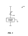
- FIG. 1 is a schematic illustration of an exemplary memory cell 100 provided in accordance with an embodiment of the present invention.
- the memory cell 100 includes a reversible resistance-switching element 102 coupled to a steering element 104.
- the reversible resistance-switching element 102 includes a reversible resistivity-switching material (not separately shown) having a resistivity that may be reversibly switched between two or more states.
- the reversible resistivity-switching material of element 102 may be in an initial, low-resistivity state upon fabrication. Upon application of a first voltage and/or current, the material is switchable to a high-resistivity state. Application of a second voltage and/or current may return the reversible resistivity-switching material to a low-resistivity state.
- the reversible resistance-switching element 102 may be in an initial, high-resistance state upon fabrication that is reversibly switchable to a low-resistance state upon application of the appropriate voltage(s) and/or current(s).
- one resistance state may represent a binary "0" while another resistance state may represent a binary "1", although more than two data/resistance states may be used.
- Numerous reversible resistivity-switching materials and operation of memory cells employing reversible resistance-switching elements are described, for example, the ⁇ 939 Application, mentioned above.
- the reversible resistance-switching element 102 us formed using a selectively deposited or grown CNT material. As will be described further below, use of a selectively formed CNT material eliminates the need to etch the CNT material. Fabrication of the reversible resistance-switching element 102 thereby is simplified.
- the steering element 104 may include a thin film transistor, a diode, or another suitable steering element that exhibits non-ohmic conduction by selectively limiting the voltage across and/or the current flow through the reversible resistance-switching element 102.
- the memory cell 100 may be used as part of a two or three dimensional memory array and data may be written to and/or read from the memory cell 100 without affecting the state of other memory cells in the array.
- Exemplary embodiments of the memory cell 100, the reversible resistance-switching element 102 and the steering element 104 are described below with reference to FIGS. 2A-5 .
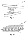
- FIG. 2A is simplified prospective view of a first embodiment of a memory cell 200 provided in accordance with the present invention.
- the memory cell 200 includes a reversible resistance-switching element 202 coupled in series with a diode 204 between a first conductor 206 and a second conductor 208.
- a barrier layer 210, a conductive layer 212 and/or a CNT seeding layer 214 may be formed between the reversible resistance-switching element 202 and the diode 204.
- the barrier layer 210 may include titanium nitride, tantalum nitride, tungsten nitride, etc.
- the conductive later 212 may include tungsten or another suitable metal layer.
- the CNT seeding layer 214 is a conducting layer that promotes CNT material formation, i.e. titanium nitride.
- the CNT seeding layer 214 is titanium or, in an arrangement not in accordance with the present invention, tantalum nitride with a surface roughed by chemical mechanical polishing (CMP) or another suitable process.
- CMP chemical mechanical polishing
- a surface roughed titanium nitride, or in arrangements not in accordance with the present invention, tantalum nitride or similar layer may be coated with a metal catalyst layer of nickel, cobalt, iron, etc., that promotes CNT material formation.
- the CNT seeding layer 214 may be a metal catalyst layer such as nickel, cobalt, iron or the like that promotes CNT formation.
- the barrier layer 210, conductive layer 212 and/or CNT seeding layer 214 may serve as a hard mask during formation of the diode 204.
- metal hard masks are described, for example, in U.S. Patent Application Serial No: 11/444,936, filed May 13, 2006 and titled “CONDUCTIVE HARD MASK TO PROTECT PATTERENED FEATURES DURING TRENCH ETCH” (hereinafter "the 936 Application”) (published as US 2007/284656 ).
- only a portion, such as one or more filaments, of the CNT material that forms the reversible resistance-switching element 202 may switch and/or be switchable.
- the diode 204 may include any suitable diode such as a vertical polycrystalline p-n or p-i-n diode, whether upward pointing with an n-region above a p-region of the diode or downward pointing with a p-region above an n-region of the diode. Exemplary embodiments of the diode 204 are described below with reference to FIG. 3A-C .
- the first and/or second conductor 206, 208 may include any suitable conductive material such as tungsten, any appropriate metal, heavily doped semiconductor material, a conductive silicide, a conductive silicide-germanide, a conductive germanide, or the like.
- the first and second conductors 206, 208 are rail-shaped and extend in different directions (e.g., substantially perpendicular to one another). Other conductor shapes and/or configurations may be used.
- barrier layers, adhesion layers, antireflection coatings and/or the like may be used with the first and/or second conductors 206 to improve device performance and/or aid in device fabrication.
- FIG. 2B is a simplified perspective view of a portion of a first memory level 218 formed from a plurality of the memory cells 200 of FIG. 2A .
- the memory array 218 is a "cross-point" array including a plurality of bit lines (second conductors 208) and word lines (first conductors 206) to which multiple memory cells are coupled (as shown).
- bit lines second conductors 208
- word lines first conductors 206
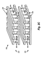
- each money level 222, 224 includes a plurality of memory cells 200 in a cross-point array. It will be understood that additional layers (e.g, an interlevel dielectric) may be present between the first and second memory levels 222 and 224, but are not shown in FIG. 2C for simplicity. Other memory array configurations may be used, as may additional levels of memory. In the embodiment of FIG.
- all diodes may "point" in the same direction, such as upward or downward depending on whether p-i-n diodes having a p-doped region on the bottom or top of the diodes are employed, simplifying diode fabrication.
- the memory levels may be formed, as described, for example, in U.S. Patent No. 6,952,030 , "High-density three-dimensional memory cell" (published as US 2005/0012119 ).
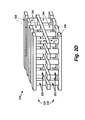
- the upper conductors of a first memory level may be used as the lower conductors of a second memory level that is positioned above the first memory level as shown in FIG. 2D .
- the diodes on adjacent memory levels preferably point in opposite directions as described in U.S. Patent Application Serial No.
- the diodes of the first memory level 222 may be upward pointing diodes as indicated by arrow A 1 (e.g., with p regions at the bottom of the diodes), while the diodes of the second memory level 224 may be downward pointing diodes as indicated by arrow A 2 (e.g., with n regions at the bottom of the diodes), or vice versa.
- a monolithic three dimensional memory array is one in which multiple memory levels are formed above a single substrate, such as a wafer, with no intervening substrates.
- the layers forming one memory level are deposited or grown directly over the layers of an existing level or levels.
- stacked memories have been constructed by forming memory levels on separate substrates and adhering the memory levels atop each other, as in Leedy, U.S. Patent No. 5,915,167 , "Three dimensional structure memory.”
- the substrates may be thinned or removed from the memory levels before bonding, but as the memory levels are initially formed over separate substrates, such memories are not true monolithic three dimensional memory arrays.
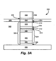
- FIG. 3A is a cross-sectional view of a first exemplary embodiment of the memory cell 200 of FIG. 2A .
- the memory cell 200 includes the reversible resistance-switching element 202, the diode 204 and the first and second conductors 206, 208.
- the diode 204 may be a vertical p-n or p-i-n diode, which may either point upward or downward.
- adjacent memory levels preferably have diodes that point in opposite directions such as downward-pointing p-i-n diodes for a first memory level and upward-pointing p-i-n diodes for an adjacent, second memory level (or vice versa).
- the diode 204 may be formed from a polycrystalline semiconductor material such as polysilicon, a polycrystalline silicon-germanium alloy, polygermanium or any other suitable material.
- the diode 204 may include a heavily doped n+ polysilicon region 302, a lightly doped or an intrinsic (unintentionally doped) polysilicon region 304 above the n+ polysilicon region 302 and a heavily doped p+ polysilicon region 306 above the intrinsic region 304.
- a thin germanium and/or silicon-germanium alloy layer may be formed on the n+ polysilicon region 302 to prevent and/or reduce dopant migration from the n+ polysilicon region 302 into the intrinsic region 304.
- a thin germanium and/or silicon-germanium alloy layer (not shown) may be formed on the n+ polysilicon region 302 to prevent and/or reduce dopant migration from the n+ polysilicon region 302 into the intrinsic region 304.
- the ⁇ 331 Application a few hundred angstroms (tens of nanometers) or less of silicon-germanium alloy with about 10 at% or more of germanium may be employed.
- a barrier layer 308, such as titanium nitride, tantalum nitride, tungsten nitride, etc., may be formed between the first conductor 206 and the n+ region 302 (eg., to prevent and/or reduce migration of metal atoms into the polysilicon regions).
- a silicide layer 310 may be formed on the diode 204 to place the deposited silicon in a low resistivity state, as fabricated.
- a low resistivity state allows for easier programming of the memory cell 200 as a large voltage is not required to switch the deposited silicon to a low resistivity state.
- a silicide-forming metal layer 312 such as titanium or cobalt may be deposited on the p+ polysilicon region 306.
- the silicide-forming metal layer 312 and the deposited silicon of the diode 204 interact to form the silicide layer 310, consuming all or a portion of the silicide-forming metal layer 312.
- silicide-forming materials such as titanium and/or cobalt react with deposited silicon during annealing to form a silicide layer.
- the lattice spacings of titanium silicide and cobalt silicide are close to that of silicon, and it appears that such silicide layers may serve as "crystallization templates" or "seeds" for adjacent deposited silicon as the deposited silicon crystallizes (e.g., the silicide layer 310 enhances the crystalline structure of the silicon diode 204 during annealing). Lower resistivity silicon thereby is provided. Similar results may be achieved for silicon-germanium alloy and/or germanium diodes.
- the reversible resistance-switching element 202 is formed by a selective fabrication process in which CNT material is formed on a patterned and etched CNT seeding layer 314.
- the CNT seeding layer 314 may be a single layer of roughened metal nitride, such as surface roughened titanium or tantalum nitride, a single layer of a metal catalyst such as nickel, cobalt, iron, etc., or a multi-layer structure formed from a smooth or surface roughened metal nitride coated with a metal catalyst.
- Exemplary CNT seeding layer materials include titanium or tantalum nitride and/or nickel, cobalt, iron or another suitable metal and/or catalyst.
- the CNT seeding layer 314 and the reversible resistance-switching element 202 may be formed over the conductive silicide-forming metal layer 312.
- the CNT seeding layer 314 and silicide-forming metal layer 312 may be patterned and etched during formation of the diode 204 as described below with reference to FIGS. 4A-4D .
- a metal hard mask may be formed over the silicide-forming metal layer 312 prior to formation of the CNT seeding layer 314 and resistance-switching element 202.
- a barrier layer 316 and/or a conductive layer 318 may be formed over the silicide-forming metal layer 312.
- the CNT seeding layer 314 then may be formed over the conductive layer 318.
- the barrier layer 316 may include titanium nitride, tantalum nitride, tungsten nitride, etc., and the conductive layer 318 may include tungsten or another suitable metal layer.
- the barrier layer 316 and/or conductive layer 318, as well as the CNT seeding layer 314, may serve as a hard mask during formation of the diode 204 and may mitigate any overetching that may occur during formation of the top conductor 208 (as described in the '936 Application).
- the CNT seeding layer 314, barrier layer 316 and conductive layer 318 may be patterned and etched, and then serve as a mask during etching of the diode 204.
- Etching of the CNT seeding layer 314, conductive layer 318, barrier layer 316, silicide-forming metal layer 312, diode 204 (p+ polysilicon layer 306, intrinsic layer 304, n+ polysilicon layer 302) and barrier layer 308 creates a pillar structure 320.
- Dielectric material 322 is deposited on top of and around the pillar structure 320 so as to isolate the pillar structure 320 from other similar pillar structures of other memory cells (not shown) fabricated on a memory level that includes the memory cell 200.
- a CMP or dielectric etchback step then is performed to planarize the dielectric material 322 and remove the dielectric material from the top of the CNT seeding later 314.
- Such a CMP or dielectric etchback step may also roughen the surface of the CNT seeding layer 314.
- the CNT seeding layer 314 may include titanium nitride that is roughened by the CMP or dielectric etchback step just described and/or by an additional roughening step.
- Such a roughened, titanium nitride surface may be employed as a seeding surface for CNT fabrication.
- roughened titanium nitride has been shown to facilitate formation of vertically aligned CNTs as described by Smith et al., "Polishing TiN for Nanotube Synthesis", Proceedings of the 16th Annual Meeting of the American Society for Precision Engineering, Nov. 10-15, 2001 . (See also Rao et al., "In situ-grown carbon nonotube array with excellent field emission characteristics", Appl. Phys. Lett., Vol. 76, No. 25, 19 June 200, pp. 3813-3815 .)
- the CNT seeding layer 314 may be about 1000 to about 5000 angstroms (about 100 to about 500 nm) of a metal nitride such as titanium or tantalum nitride with an arithmetic average surface roughness Ra of about 850 to about 4000 angstroms (about 85 to about 4000 nm), and more preferably about 4000 angstroms (about 400 nm).
- a metal nitride such as titanium or tantalum nitride with an arithmetic average surface roughness Ra of about 850 to about 4000 angstroms (about 85 to about 4000 nm), and more preferably about 4000 angstroms (about 400 nm).
- about 1 to about 200 angstroms (about 0.1 to about 20 nm), and more preferably about 20 angstroms (about 2 nm) or less, of a metal catalyst layer such as nickel, cobalt, iron, etc., may be deposited onto the surface roughened metal nitride layer prior to CNT formation.
- the CNT seeding layer 314 may include about 20 to about 500 angstroms (about 2 to about 50 nm) of non-roughened or smooth titanium, tantalum or similar metal nitride coated with about 1 to about 200 angstroms (about 0.1 to about 20 nm), and more preferably about 20 angstroms (about 2 nm) or less, of a metal catalyst layer such as nickel, cobalt, iron, etc.
- the nickel, cobalt, iron or other metal catalyst layer in any embodiment may be a continuous or non-continuous film. Other materials, thickness and surface roughnesses may be used.
- a CNT fabrication process is performed to selectively grow and/or deposit CNT material 324 on the CNT seeding layer 314.
- This CNT material 324 serves as the reversible resistance-switching element 202.
- Any suitable method may be used to form CNT material on the CNT seeding layer 314. For example, chemical vapour deposition (CVD), plasma-enhanced CVD, laser vaporization, electric arc discharge or the like may be employed.
- CNTs may be formed on a TiN seeding layer by chemical vapour deposition (CVD) at a temperature of about 675 to 700°C in xylene, argon, hydrogen and/or ferrocene at a flow rate of about 100 sccm for about 30 minutes.
- CVD chemical vapour deposition
- Other temperatures, gases, flow rates and/or growth times may be used.
- CNTs may be formed on a nickel catalyst layer by CVD at a temperature of about 650°C in about 20% C 2 H 4 and 80% Argon at a pressure of about 5.5 Torr for about 20 minutes.
- Other temperatures, gases, ratios, pressures and/or growth times may be used.
- CNTs may be formed on a metal catalyst layer such as nickel, cobalt, iron, etc., using plasma enhanced CVD at a temperature of about 600 to 900°C in about 20% methane, ethylene, acetylene or another hydrocarbon diluted with about 80% argon, hydrogen and/or ammonia using an RF power of about 100-200 Watts for about 8-30 minutes.
- a metal catalyst layer such as nickel, cobalt, iron, etc.
- CNT material 324 forms only over the CNT seeding layer 314 of pillar structure 320 (and other similar pillar structures (not shown) of other memory cells fabricated on a memory level that includes the memory cell 200).
- the CNT material 324 may have a thickness of about 1 nanometers to about 1 micron (and even tens of microns), and more preferably about 10 to about 20 nanometers, although other CNT material thicknesses may be used.
- the density of the individual tubes in the CNT material 324 may be, for example, about 6.6x10 3 to about 1x10 6 CNTs/micron 2 , and more preferably at least about 6.6x10 4 CNTs/micron 2 , although other densities may be used.
- the pillar structure 320 has a width of about 45 nanometers, in some embodiments, it is preferred to have at least about 10 CNTs, and more preferably at least about 100 CNTs, in the CNT material 324 (although fewer CNTs, such as 1, 2, 3, 4, 5, etc., or more CNTs, such as more than 100, may be employed).
- the CNT material 324 may be preferable that at least about 50%, and more preferably at least about 2/3, of the carbon nano-tubes of the CNT material 324 are semiconducting.
- multiple wall CNTs are generally metallic while single wall CNTs may be metallic or semiconducting, in one or more embodiments, it may be preferable for the CNT material 324 to include primarily semiconducting single wall CNTs. In other embodiments, fewer than 50% of the CNTs of the CNT material 324 may be semiconducting.
- the individual tubes of the CNT material 324 may be fabricated so as to be substantially vertically aligned (e.g., thereby reducing and/or preventing the state of a memory cell from being influenced or "disturbed" by the state and/or programming of adjacent memory cells). Note that this vertical alignment may or may not extend over the entire thickness of the CNT material 324. For example, during the initial growth phase, some or most of the individual tubes may be vertical aligned (e.g., not touching). However, as the individual tubes increase in length vertically, portions of the tubes may come in contact with one another, and even become entangled or entwined.
- defects may be intentionally created in the CNT material 324 to improve or otherwise tune the reversible resistivity-switching characteristics of the CNT material 324.
- argon, O 2 or another species may be implanted into the CNT material 324 to create defects in the CNT material 324.
- the CNT material 324 may be subjected or exposed to an argon or O 2 plasma (biased or chemical) to intentionally create defects in the CNT material 324.
- dielectric material 326 is deposited on top of and around the CNT material 324 so as to isolate the CNT material 324 from other similar CNT material regions of other memory cells (not shown) fabricated on a memory level that includes the memory cell 200.
- a CMP or dielectric etchback step then is performed to planarize the dielectric material 326 and remove the dielectric material from the top of the CNT material 324.
- the top conductor 208 is formed.
- one or more barrier layers and/or adhesion layers 328 may be formed over the CNT material 324/reversible resistance-switching element 202 prior to deposition of a conductive layer 330.
- the conductive layer 330 and barrier layer 328 may be patterned and/or etched together to form the top conductor 208.
- the top conductor 208 may be formed using a damascene process as described below with reference to FIGS. 4A-4D .
- the memory cell 200 may be annealed to crystallize the deposited semiconductor material of the diode 204 (and/or to form the silicide layer 310).
- the anneal may be performed for about 10 seconds to about 2 minutes in nitrogen at a temperature of about 600 to 800°C, and more preferably between about 650 and 750°C. Other annealing times, temperatures and/or environments may be used.
- the silicide layer 310 may serve as a "crystallization template" or “seed” during annealing for underlying deposited semiconductor material that forms the diode 204. Lower resistivity diode material thereby is provided.
- the CNT seeding layer 314 may include one or more additional layers.
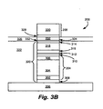
- FIG. 3B is a cross-sectional view of a second exemplary embodiment of the memory cell 200 of FIG. 2A in which the CNT seeding layer 314 includes an additional metal catalyst layer 332.
- the metal catalyst layer 332 may be selectively deposited over the CMP or etchback exposed CNT seeding layer 314.
- a nickel, cobalt, iron, etc., metal catalyst layer 332 may be selectively formed over a surface roughened titanium or tantalum nitride CNT seeding layer 314 by electroless deposition, electroplating or the like.
- the CNT material 324 then may be formed over the metal catalyst coated CNT seeding layer 314.
- metal catalyst layer 332 may eliminate the need for a catalyst precursor during CNT formation.
- Exemplary metal catalyst layer thicknesses range from about 1 to 200 angstroms, (about 0.1 to 20 nm) although other thickness may be used. Such an embodiment may be used with or without the metal hard mask layers 316 and 318.
- a nickel, cobalt, iron, or similar metal catalyst layer also may be formed over a non-surface-roughened or smooth titanium nitride, tantalum nitride or similar layer by electroless deposition, electroplating or the like.
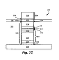
- FIG. 3C is a cross-sectional view of an exemplary arrangement of the memory cell 200 of FIG. 2A .
- the memory cell 200 of FIG. 3C is similar to the memory cell 200 of FIG. 3B , but does not include the surface roughened CNT seeding layer 314.
- no CNT seeding layer 314 is deposited over the conductive layer 318 prior to formation of the pillar structure 320.
- dielectric material 322 is deposited on top of and around the pillar structure 320 and planarized to expose the top of the conductive layer 318.
- a metal catalyst layer 332 such as nickel, cobalt, iron, etc., then is selectively deposited on the exposed conductive layer 318, and CNT material 324 may be formed over the metal catalyst layer 332.
- CNT material 324 may be formed over the metal catalyst layer 332.
- such an arrangement may be used with or without the metal hard mask layers 316 and 318.
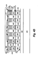
- FIGS. 4A-D illustrate cross sectional views of a portion of a substrate 400 during fabrication of a first memory level in accordance with an embodiment of the present invention.
- the first memory level includes a plurality of memory cells that each include a reversible resistance-switching element formed by selectively fabricating carbon nano-tube (CNT) material above a substrate. Additional memory levels may be fabricated above the first memory level (as described previously with reference to FIGS. 2C-2D ).
- the substrate 400 is shown as having already undergone several processing steps.
- the substrate 400 may be any suitable substrate such as a silicon, germanium, silicon-germanium, undoped, doped, bulk, silicon-on-insulator (SOI) or other substrate with or without additional circuitry.
- the substrate 400 may include one or more n-well or p-well regions (not shown).
- Isolation layer 402 is formed above the substrate 400.
- the isolation layer 402 may be a layer of silicon dioxide, silicon nitride, silicon oxynitride or any other suitable insulating layer.
- an adhesion layer 404 is formed over the isolation layer 402 (e.g., by physical vapour deposition or another method.)
- the adhesion layer 404 may be about 20 to about 500 angstroms (about 2 to about 50 nm), and preferably about 100 angstroms (about 10 nm), of titanium nitride or another suitable adhesion layer such as tantalum nitride, tungsten nitride, combinations of one or more adhesion layers, or the like. Other adhesion layer materials and/or thicknesses may be employed.
- the adhesion layer 404 may be optional.
- the conductive layer 406 may include any suitable conductive material such as tungsten or another appropriate metal, heavily doped semiconductor material, a conductive silicide, a conductive silicide-germanide, a conductive germanide, or the like deposited by any suitable method (e.g., chemical vapour deposition (CVD), physical vapor deposition (PVD), etc.).
- the conductive layer 406 may comprise about 200 to about 2500 angstroms (about 20 to about 250 nm) of tungsten. Other conductive layer materials and/or thicknesses may be used.
- the adhesion layer 404 and the conductive layer 406 are patterned and etched.
- the adhesion layer 404 and the conductive layer 406 may be patterned and etched using conventional lithography techniques, with a soft or hard mask, and wet or dry etch processing.
- the adhesion layer 404 and conductive layer 406 are patterned and etched so as to form substantially parallel, substantially co-planner conductors 408 (as shown in FIG. 4A ).
- Exemplary widths for the conductors 408 and/or spacings between the conductors 408 range from about 200 to about 2500 angstroms (about 20 to about 250 nm), although other conductor widths and/or spacings may be used.
- a dielectric layer 410 is formed over the substrate 400 so as to fill the voids between the conductors 408.
- a dielectric layer 410 is formed over the substrate 400 so as to fill the voids between the conductors 408.
- approximately 3000-7000 angstroms (approximately 300-700 nm) of silicon dioxide may be deposited on the substrate 400 and planarized using chemical mechanical polishing or an etchback process to form a planner
- planar surface 412 includes exposed top surfaces of the conductors 408 separated by dielectric material (as shown).
- dielectric material such as silicon nitride, silicon oxynitride, low K dielectrics, etc., and/or other dielectric layer thicknesses may be used.
- Exemplary low K dielectrics include carbon doped oxides, silicon carbon layers, or the like.
- the conductors 408 may be formed using a damascene process in which the dielectric layer 410 is formed, patterned and etched to create openings or voids for the conductors 408.
- the openings or voids then may be filled with the adhesion layer 404 and the conductive layer 406 (and/or a conductive seed, conductive fill and/or barrier layer if needed).
- the adhesion layer 404 and conductive layer 406 then may be planarized to form the planar surface 412. In such an embodiment, the adhesion layer 404 will line the bottom and sidewalls of each opening or void.
- a barrier layer 414 is formed over the planarized top surface 412 of the substrate 400.
- the barrier layer 414 may be about 20 to about 500 angstroms (about 2 to about 50 nm), and preferably about 100 angstroms (about 10 nm), of titanium nitride or another suitable barrier layer such as tantalum nitride, tungsten nitride, combinations of one or more barrier layers, barrier layers in combination with other layers such as titanium/titanium nitride, tantalum/tantalum nitride or tungsten/tungsten nitride stacks, or the like. Other barrier layer materials and/or thicknesses may be employed.
- each memory cell After deposition of the barrier layer 414, deposition of the semiconductor material used to form the diode each memory cell begins (e.g., diode 204 in FIGS. 2A-3 ).
- Each diode may be a vertical p-n or p-i-n diode as previously described.
- each diode is formed from a polycrystalline semiconductor material such as polysilicon, a polycrystalline silicon-germanium alloy, polygermanium or any other suitable material.
- a polysilicon downward-pointing diode is described herein. It will be understood that other materials and/or diode configurations may be used.
- n+ silicon layer 416 is deposited on the barrier layer 414.
- the n+ silicon layer 416 is in an amorphous state as deposited.
- the n+ silicon layer 416 is in a polycrystalline state as deposited.
- CVD or another suitable process may be employed to deposit the n+ silicon layer 416.
- the n+ silicon layer 416 may be formed for example, from about 100 to about 1000 angstroms (about 10 to about 100 nm), preferably about 100 angstroms (about 10 nm), of phosphorous or arsenic doped silicon having a doping concentration of about 10 21 cm -3 .
- n+ silicon layer 416 may be doped in situ, for example, by flowing a donor gas during deposition. Other doping methods may be used (e.g., implantation).
- a lightly doped, intrinsic and/or unintentionally doped silicon layer 418 is formed over the n+ silicon layer 416.
- the intrinsic silicon layer 418 is in an amorphous state as deposited. In other embodiments, the intrinsic silicon layer 418 is in a polycrystalline state as deposited. CVD or another suitable deposition method may be employed to deposit the intrinsic silicon layer 418.
- the intrinsic silicon 418 may be about 500 to about 4800 angstroms (about 50 to about 480 nm), preferably about 2500 angstroms (about 250 nm), in thickness. Other intrinsic layer thicknesses may be used.
- a thin (e.g., a few hundred angstroms (nm)or less) germanium and/or silicon-germanium alloy layer may be formed on the n+ silicon layer 416 prior to deposition of the intrinsic silicon layer 418 to prevent and/or reduce dopant migration from the n+ silicon layer 416 into the intrinsic silicon layer 418 (as described in the '331 Application, previously mentioned).
- Heavily doped, p-type silicon is either deposited and doped by ion implantation or is doped in situ during deposition to form a p+ silicon layer 420.
- a blanket p+ implant may be employed to implant boron a predetermined depth within the intrinsic silicon layer 418.
- Exemplary implantable molecular ions include BF 2 , BF 3 , B and the like.
- an implant dose of about 1-5x10 15 ions/cm 2 may be employed.
- Other implant species and/or doses may be used.
- a diffusion process may be employed.
- the resultant p+ silicon layer 420 has a thickness of about 100-700 angstroms (10-70 nm), although other p+ silicon later sizes may be used.
- a silicide-forming metal layer 422 is deposited over the p+ silicon layer 420.
- exemplary silicide-forming metals include sputter or otherwise deposited titanium or cobalt.
- the silicide-forming metal layer 422 has thickness of about 10 to about 200 angstroms (about 1 to about 20 nm), preferably about 20 to about 50 angstroms (about 2 to about 5 nm) and more preferably about 20 angstroms (about 2 nm).
- Other silicide-forming metal layer materials and/or thicknesses may be used.
- a barrier layer 424 is deposited over the silicide-forming metal layer 422.
- the barrier layer 424 may be about 20 to 500 angstroms (about 2 to about 50 nm), and preferably about 100 angstroms (about 10 nm), of titanium nitride or another suitable barrier layer such as tantalum nitride, tungsten nitride, combinations of one or more barrier layers, barrier layers in combination with other layers such as titanium/titanium nitride, tantalum/tantalum nitride or tungsten/tungsten nitride stacks, or the like. Other barrier layer materials and/or thicknesses may be employed.
- the conductive layer 426 may be about 50 to about 1000 angstroms (about 5 to about 100 nm), and preferably about 500 angstroms (about 50 nm) of conductive material such as tungsten or another suitable metal.
- a CNT seeding layer 427 is formed over the conductive layer 426.
- the CNT seeding layer 427 may be about 1000 to about 5000 angstroms (about 100 to about 500 nm) of titanium or tantalum nitride, although other thicknesses may be used.
- the barrier layer 414, silicon regions 416, 418 and 420, silicide-forming metal layer 422, barrier layer 424, conductive layer 426 and CNT seeding layer 427 are then patterned and etched into pillars 428. For example, initially, the CNT seeding layer 427, conductive layer 426 and barrier layer 424 are etched. The etch continues, etching silicide-forming metal layer 422, silicon regions 420, 418 and 416 barrier layer 414. CNT seeding layer 427, conductive layer 426 and barrier layer 414 serve as a hard mask during the silicon etch.
- a hard mask is an etched layer which serves to pattern the etch of an underlying layer; if all of the photoresist present on the CNT seeding layer 427 has been consumed, the hard mask can provide the pattern in its stead.
- the pillars 428 are formed in a single photolithographic step. Conventional lithography techniques, and wet or dry etch processing may be employed to form the pillars 428.
- Each pillar 428 includes p-i-n, downward-pointing diode 430. Upward-pointing p-i-n diodes may be similarly formed.
- a dielectric layer 432 is deposited over the pillars 428 to fill the voids between the pillars 428.
- a dielectric layer 432 is deposited over the pillars 428 to fill the voids between the pillars 428.
- approximately 200-7000 angstroms (approximately 20-700 nm) of silicon dioxide may be deposited and planarized using chemical mechanical polishing or an etchback process to form a planar surface 434.
- the planar surface 434 includes exposed top surfaces of the pillars 428 separated by dielectric material 432 (as shown).
- Other dielectric materials such as silicon nitride, silicon oxynitirde, low K dielectrics, etc., and/or other dielectric layer thicknesses may be used.
- Exemplary low K dielectrics include carbon doped oxides, silicon carbon layers, or the like.
- CNT material 436 ( FIG. 4C ) is selectively formed on the CNT seeding layer 427 of each pillar 428.
- the CNT seeding layer 427 is titanium nitride, tantalum nitride or a similar material, the surface of the CNT seeding layer 427 may be roughened to allow CNTs to be formed directly on the CNT seeding layer 427.
- the CNT seeding layer 427 may be roughened so as to have an arithmetic average surface roughness Ra of at least about 850 to 4000 angstroms (about 85 to 400 nm), and more preferably at least about 4000 angstroms (about 400 nm). Other surface roughnesses may be employed.
- an additional metal catalyst/seeding layer such as nickel, cobalt, iron, etc., may be selectively deposited over a surface-roughened CNT seeding layer 427 prior to formation of the CNT material 436 to provide the benefits a metal catalyst during CNT formation (as described previously with reference to FIG. 3B ).
- a metal catalyst later may be used without an underlying, surface roughened seeding layer (as described previously with reference to FIG. 3C ).
- a CNT fabrication process is performed to selectively grow and/or deposit CNT material 436 on each pillar 428.
- This CNT material 436 serves as the reversible resistance-switching element 202.
- Any suitable method may be used to from CNT material 436 on each pillar 428. For example, chemical vapour deposition (CVD), plasma-enhanced CVD, laser vaporization, electric arc discharge or the like may be employed.
- CNTs may be formed on a TiN seeding layer by chemical vapour deposition (CVD) at a temperature of about 675 to 700°C in xylene, argon, hydrogen and/or ferrocene at a flow rate of about 100 sccm for about 30 minutes.
- CVD chemical vapour deposition
- Other temperatures, gases, flow rates and/or growth times may be used.
- CNTS may be formed on a nickel catalyst later by CVD at a temperature of about 650°C in about 20% C 2 H 4 and 80% Argon at a pressure of about 5.5 Torr for about 20 minutes.
- Other temperatures, gases, ratios, pressures and/or growth times may be used.
- CNTs may be formed on a metal catalyst layer such as nickel, cobalt, iron, etc., using plasma enhanced CVD at a temperature of about 600 to 900°C in about 20% methane, ethylene, acetylene or another hydrocarbon diluted with about 80% argon, hydrogen and/or ammonia using an RF power of about 100-200 Watts for about 8-30 minutes.
- a metal catalyst layer such as nickel, cobalt, iron, etc.
- CNT material 436 forms only over the CNT seeding layer 427 of each pillar 428.
- the CNT material 436 may have a thickness of about 1 nanometers to about 1 micron (and even tens of microns), and more preferably about 10 to about 20 nanometers, although other CNT material thicknesses may be used.
- the density of individual tubes in the CNT material 436 may be, for example, about 6.6x10 3 to about 1x10 6 CNTs/micron 2 , and more preferably at least about 6.6x10 4 CNTs/micron 2 , although other densities may be used.
- the pillars 428 have a width of about 45 nanometers, in some embodiments, it is preferred to have at least about 10 CNTs, and more preferably at least about 100 CNTS, in the CNT material 436 formed on each pillar 428 (although fewer CNTs, such as 1, 2, 3, 4, 5, etc., or more CNTs, such as more than 100, may be employed).
- dielectric material 437 is deposited on top of and around the regions of CNT material 436 so as to isolate adjacent CNT material regions from one another.
- a CMP or dielectric material 427 and remove the dielectric material from the top of the regions of CNT material 436.
- silicon dioxide approximately 200-7000 angstroms (approximately 20-700 nm), and in some embodiments a micron or more, of silicon dioxide may be deposited and planarized using chemical mechanical polishing or an etchback process.
- Other dielectric materials such as silicon nitride, silicon oxynitride, low K dielectrics, etc., and/or other dielectric layer thicknesses may be used.
- Exemplary low K dielectrics include carbon doped oxides, silicon carbon layers, or the like.
- a second set of conductors 438 may be formed above the pillars 428 in a manner similar to the formation of the bottom set of conductors 408.
- one or more barrier layers and/or adhesion layers 440 may be deposited over the reversible resistance-switching elements 436 prior to deposition of a conductive layer 442 used to form the upper, second set of conductors 438.
- the conductive layer 442 may be formed from any suitable conductive material such as tungsten, another suitable metal, heavily doped semiconductor material, a conductive silicide, a conductive silicide-germanide, a conductive germanide, or the like deposited by any suitable method (e.g., CVD, PVD, etc.). Other conductive layer materials may be used.
- Barrier layers and/or adhesion layers 440 may include titanium nitride or another suitable layer such as tantalum nitride, tungsten nitride, combinations of one or more layers, or any other suitable material(s).
- the deposited conductive layer 442 and barrier and/or adhesion layer 440 may be patterned and etched to form the second set of conductors 438.
- the upper conductors 438 are substantially parallel, substantially coplanar conductors that extend in a different direction than the lower conductors 408.
- the upper conductors 438 may be formed using a damascene process in which a dielectric layer is formed, patterned and etched to create openings or voids for the conductors 438.
- the conductive layer 426 and barrier layer 424 may mitigate the affects of overetching of such a dielectric layer during formation of the openings or voids for the upper conductors 438, preventing accidental shorting of the diodes 430.
- the openings or voids may be filled with the adhesion layer 440 and the conductive layer 442 (and/or a conductive seed, conductive fill and/or barrier layer if needed).
- the adhesion layer 440 and conductive layer 442 then may be planarized to form a planar surface.
- the resultant structure may be annealed to crystallize the deposited semiconductor material of the diodes 430 (and/or to form silicide regions by reaction of the silicide-forming metal layer 422 with p+ region 420).
- the anneal may be performed for about 10 seconds to about 2 minutes in nitrogen at a temperature of about 600 to 800°C, and more preferably between about 650 and 750°C. Other annealing times, temperatures and/or environments may be used.
- the silicide regions formed as each silicide-forming metal layer region 422 and p+ region 420 react may serve as "crystallization templates" or “seeds" during annealing for underlying deposited semiconductor material that forms the diodes 430 (e.g., changing any amorphous semiconductor material to polycrystalline semiconductor material and/or improving overall crystalline properties of the diodes 430). Lower resistivity diode material thereby is provided.
- FIG. 5 is a cross sectional view of an exemplary memory cell 500 provided in accordance with the present invention.
- the memory cell 500 includes a thin film transistor (TFT), such as a thin film, metal oxide semiconductor field effect transistor (MOSFET) 502 coupled to a reversible resistance-switching element 504 formed above a substrate 505.
- TFT thin film transistor
- MOSFET metal oxide semiconductor field effect transistor
- the MOSFET 502 may be an n-channel or a p-channel thin film MOSFET formed on any suitable substrate.
- an insulating region 506 such as silicon dioxide, silicon nitride, oxynitride, etc., is formed above the substrate 505 and a deposited semiconductor region 507 such as deposited silicon, germanium, silicon-germanium, etc., is formed above the insulating region 506.
- the thin film MOSFET 502 is formed within the deposited semiconductor region 507 and is insulated from the substrate 505 by the insulating region 506.
- the MOSFET 502 includes source/drain regions 508, 510 and channel region 512, as well as gate dielectric layer 514, gate electrode 516 and spacers 518a-b.
- the source/drain regions 508, 510 may be doped p-type and the channel region 512 may be doped n-type, while in other embodiments the source/drain regions 508, 510 may be doped n-type and the channel region 512 may be doped p-type.
- Any other MOSFET configuration or any suitable fabrication techniques may be employed for the thin film MOSFET 502.
- the MOSFET 502 may be electrically isolated by isolation regions (not shown) formed using an STI, LOCOS or other similar process.
- gate, source and/or drain regions of the MOSFET 502 may be shared with other transistors (not shown) formed on the substrate 505.
- the reversible resistance-switching element 504 includes a reversible resistivity-switching CNT material 522 formed over a conductive plug 526.
- the reversible resistivity-switching CNT material 522 is formed using a selective formation process as previously described with reference to the embodiments of FIGS. 1-4D .
- a CNT seeding layer 524 such as titanium or tantalum nitride and/or a metal catalyst such as nickel, cobalt, iron, etc., may be formed over the conductive plug 526.
- the CNT material 522 then may be selectively formed over the CNT seeding layer 524 as previously described.
- the reversible resistance-switching element 504 is coupled to the source/drain region 510 of the MOSFET 502 by the first conductive plug 526 and to a first metal level (Ml) line 528 by a second conductive plug 530 (which extend through a dielectric layer 532).
- a third conductive plug 534 couples the source/drain region 508 of the MOSFET 502 to an M1 line 536.
- the conductive plugs and/or lines may be formed from any suitable materials (without or without barriers layers) such as tungsten, another metal, heavily doped semiconductor material, a conductive silicide, a conductive silicide-germanide, a conductive germanide, or the like.
- the dielectric layer 532 may include any suitable dielectric such as silicon dioxide, silicon nitride, silicon oxynitride, low K dielectrics, etc.
- the thin film MOSFET 502 operates as a steering element in a manner similar to that of the diodes employed in the memory cells of FIGS. 2A-4D , selectively limiting the voltage applied across and/or the current flow though the reversible resistance-switching element 504.
Landscapes
- Engineering & Computer Science (AREA)
- Chemical & Material Sciences (AREA)
- Nanotechnology (AREA)
- Crystallography & Structural Chemistry (AREA)
- Manufacturing & Machinery (AREA)
- Physics & Mathematics (AREA)
- Mathematical Physics (AREA)
- Theoretical Computer Science (AREA)
- Semiconductor Memories (AREA)
- Carbon And Carbon Compounds (AREA)
Applications Claiming Priority (2)
| Application Number | Priority Date | Filing Date | Title |
|---|---|---|---|
| US11/968,154 US8236623B2 (en) | 2007-12-31 | 2007-12-31 | Memory cell that employs a selectively fabricated carbon nano-tube reversible resistance-switching element and methods of forming the same |
| PCT/US2008/088584 WO2009088888A2 (en) | 2007-12-31 | 2008-12-30 | Memory cell that employs a selectively fabricated carbon nano-tube reversible resistance-switching element and methods of forming the same |
Publications (3)
| Publication Number | Publication Date |
|---|---|
| EP2227824A2 EP2227824A2 (en) | 2010-09-15 |
| EP2227824A4 EP2227824A4 (en) | 2010-12-15 |
| EP2227824B1 true EP2227824B1 (en) | 2014-04-16 |
Family
ID=40798167
Family Applications (1)
| Application Number | Title | Priority Date | Filing Date |
|---|---|---|---|
| EP08869555.6A Not-in-force EP2227824B1 (en) | 2007-12-31 | 2008-12-30 | Memory cell that employs a selectively fabricated carbon nano-tube reversible resistance-switching element and methods of forming the same |
Country Status (7)
Families Citing this family (71)
| Publication number | Priority date | Publication date | Assignee | Title |
|---|---|---|---|---|
| US9390790B2 (en) | 2005-04-05 | 2016-07-12 | Nantero Inc. | Carbon based nonvolatile cross point memory incorporating carbon based diode select devices and MOSFET select devices for memory and logic applications |
| US9287356B2 (en) * | 2005-05-09 | 2016-03-15 | Nantero Inc. | Nonvolatile nanotube diodes and nonvolatile nanotube blocks and systems using same and methods of making same |
| US8000127B2 (en) * | 2009-08-12 | 2011-08-16 | Nantero, Inc. | Method for resetting a resistive change memory element |
| US7479654B2 (en) | 2005-05-09 | 2009-01-20 | Nantero, Inc. | Memory arrays using nanotube articles with reprogrammable resistance |
| US8183665B2 (en) * | 2005-11-15 | 2012-05-22 | Nantero Inc. | Nonvolatile nanotube diodes and nonvolatile nanotube blocks and systems using same and methods of making same |
| US9911743B2 (en) | 2005-05-09 | 2018-03-06 | Nantero, Inc. | Nonvolatile nanotube diodes and nonvolatile nanotube blocks and systems using same and methods of making same |
| US7835170B2 (en) * | 2005-05-09 | 2010-11-16 | Nantero, Inc. | Memory elements and cross point switches and arrays of same using nonvolatile nanotube blocks |
| US8217490B2 (en) * | 2005-05-09 | 2012-07-10 | Nantero Inc. | Nonvolatile nanotube diodes and nonvolatile nanotube blocks and systems using same and methods of making same |
| US8513768B2 (en) * | 2005-05-09 | 2013-08-20 | Nantero Inc. | Nonvolatile nanotube diodes and nonvolatile nanotube blocks and systems using same and methods of making same |
| US7781862B2 (en) * | 2005-05-09 | 2010-08-24 | Nantero, Inc. | Two-terminal nanotube devices and systems and methods of making same |
| US7575693B2 (en) | 2005-05-23 | 2009-08-18 | Nantero, Inc. | Method of aligning nanotubes and wires with an etched feature |
| US8558220B2 (en) * | 2007-12-31 | 2013-10-15 | Sandisk 3D Llc | Memory cell that employs a selectively fabricated carbon nano-tube reversible resistance-switching element formed over a bottom conductor and methods of forming the same |
| US8878235B2 (en) * | 2007-12-31 | 2014-11-04 | Sandisk 3D Llc | Memory cell that employs a selectively fabricated carbon nano-tube reversible resistance-switching element and methods of forming the same |
| US20090166610A1 (en) * | 2007-12-31 | 2009-07-02 | April Schricker | Memory cell with planarized carbon nanotube layer and methods of forming the same |
| US8304284B2 (en) * | 2008-04-11 | 2012-11-06 | Sandisk 3D Llc | Memory cell that employs a selectively fabricated carbon nano-tube reversible resistance-switching element, and methods of forming the same |
| US8110476B2 (en) * | 2008-04-11 | 2012-02-07 | Sandisk 3D Llc | Memory cell that includes a carbon-based memory element and methods of forming the same |
| WO2009126846A1 (en) * | 2008-04-11 | 2009-10-15 | Sandisk 3D, Llc | Damascene integration methods for graphitic films in three-dimensional memories and memories formed therefrom |
| WO2009126891A1 (en) * | 2008-04-11 | 2009-10-15 | Sandisk 3D, Llc | Methods for etching carbon nano-tube films for use in non-volatile memories |
| CN102027610B (zh) * | 2008-04-11 | 2012-12-05 | 桑迪士克3D有限责任公司 | 包括碳纳米管可逆电阻切换元件的存储器单元及其形成方法 |
| US8530318B2 (en) * | 2008-04-11 | 2013-09-10 | Sandisk 3D Llc | Memory cell that employs a selectively fabricated carbon nano-tube reversible resistance-switching element formed over a bottom conductor and methods of forming the same |
| US8133793B2 (en) | 2008-05-16 | 2012-03-13 | Sandisk 3D Llc | Carbon nano-film reversible resistance-switchable elements and methods of forming the same |
| US8569730B2 (en) * | 2008-07-08 | 2013-10-29 | Sandisk 3D Llc | Carbon-based interface layer for a memory device and methods of forming the same |
| US8309407B2 (en) * | 2008-07-15 | 2012-11-13 | Sandisk 3D Llc | Electronic devices including carbon-based films having sidewall liners, and methods of forming such devices |
| TW201021161A (en) * | 2008-07-18 | 2010-06-01 | Sandisk 3D Llc | Carbon-based resistivity-switching materials and methods of forming the same |
| US8557685B2 (en) * | 2008-08-07 | 2013-10-15 | Sandisk 3D Llc | Memory cell that includes a carbon-based memory element and methods of forming the same |
| US8319205B2 (en) * | 2008-08-14 | 2012-11-27 | Nantero Inc. | Nonvolatile nanotube programmable logic devices and a nonvolatile nanotube field programmable gate array using same |
| US9263126B1 (en) | 2010-09-01 | 2016-02-16 | Nantero Inc. | Method for dynamically accessing and programming resistive change element arrays |
| WO2010022097A1 (en) * | 2008-08-19 | 2010-02-25 | Sandisk 3D, Llc | Methods for increasing carbon nano-tube (cnt) yield in memory devices |
| KR20110080166A (ko) * | 2008-10-23 | 2011-07-12 | 쌘디스크 3디 엘엘씨 | 감소된 박리를 나타내는 탄소계 메모리 소자와 상기 소자를 형성하는 방법 |
| US20100108976A1 (en) * | 2008-10-30 | 2010-05-06 | Sandisk 3D Llc | Electronic devices including carbon-based films, and methods of forming such devices |
| US8835892B2 (en) * | 2008-10-30 | 2014-09-16 | Sandisk 3D Llc | Electronic devices including carbon nano-tube films having boron nitride-based liners, and methods of forming the same |
| US8421050B2 (en) * | 2008-10-30 | 2013-04-16 | Sandisk 3D Llc | Electronic devices including carbon nano-tube films having carbon-based liners, and methods of forming the same |
| US7915637B2 (en) * | 2008-11-19 | 2011-03-29 | Nantero, Inc. | Switching materials comprising mixed nanoscopic particles and carbon nanotubes and method of making and using the same |
| JP2010157569A (ja) * | 2008-12-26 | 2010-07-15 | Funai Electric Advanced Applied Technology Research Institute Inc | メモリセルアレイ |
| US8470646B2 (en) * | 2008-12-31 | 2013-06-25 | Sandisk 3D Llc | Modulation of resistivity in carbon-based read-writeable materials |
| US8183121B2 (en) * | 2009-03-31 | 2012-05-22 | Sandisk 3D Llc | Carbon-based films, and methods of forming the same, having dielectric filler material and exhibiting reduced thermal resistance |
| US8509124B2 (en) * | 2009-04-03 | 2013-08-13 | Lg Electronics Inc. | Method for transceiving a signal in wireless communication system |
| US8551855B2 (en) * | 2009-10-23 | 2013-10-08 | Sandisk 3D Llc | Memory cell that includes a carbon-based reversible resistance switching element compatible with a steering element, and methods of forming the same |
| US8481396B2 (en) * | 2009-10-23 | 2013-07-09 | Sandisk 3D Llc | Memory cell that includes a carbon-based reversible resistance switching element compatible with a steering element, and methods of forming the same |
| US8551850B2 (en) * | 2009-12-07 | 2013-10-08 | Sandisk 3D Llc | Methods of forming a reversible resistance-switching metal-insulator-metal structure |
| US8222704B2 (en) * | 2009-12-31 | 2012-07-17 | Nantero, Inc. | Compact electrical switching devices with nanotube elements, and methods of making same |
| US8450181B2 (en) * | 2010-01-08 | 2013-05-28 | Sandisk 3D Llc | In-situ passivation methods to improve performance of polysilicon diode |
| US20110186799A1 (en) * | 2010-02-04 | 2011-08-04 | Sandisk 3D Llc | Non-volatile memory cell containing nanodots and method of making thereof |
| US8389375B2 (en) * | 2010-02-11 | 2013-03-05 | Sandisk 3D Llc | Memory cell formed using a recess and methods for forming the same |
| US8237146B2 (en) * | 2010-02-24 | 2012-08-07 | Sandisk 3D Llc | Memory cell with silicon-containing carbon switching layer and methods for forming the same |
| US20110210306A1 (en) * | 2010-02-26 | 2011-09-01 | Yubao Li | Memory cell that includes a carbon-based memory element and methods of forming the same |
| US8481394B2 (en) * | 2010-03-04 | 2013-07-09 | Sandisk 3D Llc | Memory cell that includes a carbon-based memory element and methods of forming the same |
| US8471360B2 (en) | 2010-04-14 | 2013-06-25 | Sandisk 3D Llc | Memory cell with carbon switching material having a reduced cross-sectional area and methods for forming the same |
| KR101110543B1 (ko) | 2010-04-21 | 2012-02-09 | 주식회사 하이닉스반도체 | 고집적 반도체 장치 |
| US8436447B2 (en) | 2010-04-23 | 2013-05-07 | Sandisk 3D Llc | Memory cell that includes a carbon-based memory element and methods of forming the same |
| JP2012019191A (ja) * | 2010-06-10 | 2012-01-26 | Toshiba Corp | 不揮発性記憶装置の製造方法 |
| US8883589B2 (en) | 2010-09-28 | 2014-11-11 | Sandisk 3D Llc | Counter doping compensation methods to improve diode performance |
| CN102117823B (zh) * | 2010-11-04 | 2013-02-13 | 中国科学院上海微系统与信息技术研究所 | 电阻转换存储纳米结构及其自对准制造方法 |
| US9018692B2 (en) * | 2011-01-19 | 2015-04-28 | Macronix International Co., Ltd. | Low cost scalable 3D memory |
| KR20120137862A (ko) * | 2011-06-13 | 2012-12-24 | 삼성전자주식회사 | 3차원 더블 크로스 포인트 어레이를 갖는 반도체 메모리 소자 및 그 제조방법 |
| US9054295B2 (en) * | 2011-08-23 | 2015-06-09 | Micron Technology, Inc. | Phase change memory cells including nitrogenated carbon materials, methods of forming the same, and phase change memory devices including nitrogenated carbon materials |
| JP5564023B2 (ja) | 2011-09-08 | 2014-07-30 | 株式会社東芝 | 不揮発性記憶装置の製造方法 |
| US9029936B2 (en) | 2012-07-02 | 2015-05-12 | Sandisk Technologies Inc. | Non-volatile memory structure containing nanodots and continuous metal layer charge traps and method of making thereof |
| US8823075B2 (en) | 2012-11-30 | 2014-09-02 | Sandisk Technologies Inc. | Select gate formation for nanodot flat cell |
| US8987802B2 (en) | 2013-02-28 | 2015-03-24 | Sandisk Technologies Inc. | Method for using nanoparticles to make uniform discrete floating gate layer |
| US9331181B2 (en) | 2013-03-11 | 2016-05-03 | Sandisk Technologies Inc. | Nanodot enhanced hybrid floating gate for non-volatile memory devices |
| US9214351B2 (en) | 2013-03-12 | 2015-12-15 | Macronix International Co., Ltd. | Memory architecture of thin film 3D array |
| US9177808B2 (en) | 2013-05-21 | 2015-11-03 | Sandisk Technologies Inc. | Memory device with control gate oxygen diffusion control and method of making thereof |
| US8969153B2 (en) | 2013-07-01 | 2015-03-03 | Sandisk Technologies Inc. | NAND string containing self-aligned control gate sidewall cladding |
| US9559113B2 (en) | 2014-05-01 | 2017-01-31 | Macronix International Co., Ltd. | SSL/GSL gate oxide in 3D vertical channel NAND |
| US9923139B2 (en) | 2016-03-11 | 2018-03-20 | Micron Technology, Inc. | Conductive hard mask for memory device formation |
| US9947400B2 (en) | 2016-04-22 | 2018-04-17 | Nantero, Inc. | Methods for enhanced state retention within a resistive change cell |
| US10355206B2 (en) * | 2017-02-06 | 2019-07-16 | Nantero, Inc. | Sealed resistive change elements |
| KR102767605B1 (ko) * | 2017-02-20 | 2025-02-17 | 에스케이하이닉스 주식회사 | 카본 나노 튜브들을 갖는 시냅스를 포함하는 뉴로모픽 소자 |
| CN110085589B (zh) * | 2018-01-26 | 2021-03-26 | 中芯国际集成电路制造(天津)有限公司 | 碳纳米管模块、半导体器件及制造方法 |
| US11349071B2 (en) * | 2019-11-04 | 2022-05-31 | Globalfoundries Singapore Pte. Ltd. | Memory device and a method for forming the memory device |
Family Cites Families (49)
| Publication number | Priority date | Publication date | Assignee | Title |
|---|---|---|---|---|
| AU2136197A (en) | 1996-03-01 | 1997-09-16 | Micron Technology, Inc. | Novel vertical diode structures with low series resistance |
| US5915167A (en) | 1997-04-04 | 1999-06-22 | Elm Technology Corporation | Three dimensional structure memory |
| US6034882A (en) | 1998-11-16 | 2000-03-07 | Matrix Semiconductor, Inc. | Vertically stacked field programmable nonvolatile memory and method of fabrication |
| US6706402B2 (en) | 2001-07-25 | 2004-03-16 | Nantero, Inc. | Nanotube films and articles |
| US6858481B2 (en) | 2001-08-13 | 2005-02-22 | Advanced Micro Devices, Inc. | Memory device with active and passive layers |
| US7038935B2 (en) | 2002-08-02 | 2006-05-02 | Unity Semiconductor Corporation | 2-terminal trapped charge memory device with voltage switchable multi-level resistance |
| WO2004061851A2 (en) | 2002-12-19 | 2004-07-22 | Matrix Semiconductor, Inc | An improved method for making high-density nonvolatile memory |
| US6946719B2 (en) | 2003-12-03 | 2005-09-20 | Matrix Semiconductor, Inc | Semiconductor device including junction diode contacting contact-antifuse unit comprising silicide |
| US7176064B2 (en) | 2003-12-03 | 2007-02-13 | Sandisk 3D Llc | Memory cell comprising a semiconductor junction diode crystallized adjacent to a silicide |
| US7767499B2 (en) | 2002-12-19 | 2010-08-03 | Sandisk 3D Llc | Method to form upward pointing p-i-n diodes having large and uniform current |
| WO2004084229A1 (en) | 2003-03-18 | 2004-09-30 | Kabushiki Kaisha Toshiba | Programmable resistance memory device |
| EP1623203A4 (en) * | 2003-05-14 | 2010-11-24 | Nantero Inc | DETECTION PLATFORM USING NON-HORIZONTAL NANOTUBULAR ELEMENT |
| JP4208668B2 (ja) * | 2003-08-22 | 2009-01-14 | 富士通株式会社 | 半導体装置およびその製造方法 |
| JP4769931B2 (ja) * | 2004-02-16 | 2011-09-07 | 国立大学法人名古屋大学 | カーボンナノチューブに対する電極の形成方法及びそれを用いたカーボンナノチューブfet |
| US7135773B2 (en) * | 2004-02-26 | 2006-11-14 | International Business Machines Corporation | Integrated circuit chip utilizing carbon nanotube composite interconnection vias |
| US7405465B2 (en) | 2004-09-29 | 2008-07-29 | Sandisk 3D Llc | Deposited semiconductor structure to minimize n-type dopant diffusion and method of making |
| US7405165B2 (en) * | 2004-11-05 | 2008-07-29 | Taiwan Semiconductor Manufacturing Co, Ltd | Dual-tank etch method for oxide thickness control |
| GB0426863D0 (en) | 2004-12-07 | 2005-01-12 | Univ Southampton | Method of manufacturing carbon nanotubes |
| US7208372B2 (en) | 2005-01-19 | 2007-04-24 | Sharp Laboratories Of America, Inc. | Non-volatile memory resistor cell with nanotip electrode |
| US7579631B2 (en) | 2005-03-22 | 2009-08-25 | Spansion Llc | Variable breakdown characteristic diode |
| US7145824B2 (en) | 2005-03-22 | 2006-12-05 | Spansion Llc | Temperature compensation of thin film diode voltage threshold in memory sensing circuit |
| US9196615B2 (en) * | 2005-05-09 | 2015-11-24 | Nantero Inc. | Nonvolatile nanotube diodes and nonvolatile nanotube blocks and systems using same and methods of making same |
| US7781862B2 (en) * | 2005-05-09 | 2010-08-24 | Nantero, Inc. | Two-terminal nanotube devices and systems and methods of making same |
| US20060250836A1 (en) | 2005-05-09 | 2006-11-09 | Matrix Semiconductor, Inc. | Rewriteable memory cell comprising a diode and a resistance-switching material |
| US7479654B2 (en) | 2005-05-09 | 2009-01-20 | Nantero, Inc. | Memory arrays using nanotube articles with reprogrammable resistance |
| US7812404B2 (en) * | 2005-05-09 | 2010-10-12 | Sandisk 3D Llc | Nonvolatile memory cell comprising a diode and a resistance-switching material |
| US8470709B2 (en) | 2005-06-17 | 2013-06-25 | Imec | Formation of metal-containing nano-particles for use as catalysts for carbon nanotube synthesis |
| US7286388B1 (en) | 2005-06-23 | 2007-10-23 | Spansion Llc | Resistive memory device with improved data retention |
| US7482653B2 (en) | 2005-07-20 | 2009-01-27 | Micron Technology, Inc. | Non-volatile memory with carbon nanotubes |
| JP2007049084A (ja) | 2005-08-12 | 2007-02-22 | Toshiba Corp | スイッチ素子、メモリ素子および磁気抵抗効果素子 |
| US20070238319A1 (en) | 2005-08-31 | 2007-10-11 | Jewell-Larsen Nels E | Mechanically actuated nanotube switches |
| KR100682952B1 (ko) * | 2005-08-31 | 2007-02-15 | 삼성전자주식회사 | 나노탄성 메모리 소자 및 그 제조 방법 |
| JP5037804B2 (ja) * | 2005-09-30 | 2012-10-03 | 富士通株式会社 | 垂直配向カーボンナノチューブを用いた電子デバイス |
| KR100695164B1 (ko) | 2005-11-09 | 2007-03-14 | 삼성전자주식회사 | 스위칭 소자로서 트랜지스터 및 다이오드를 포함하는하이브리드 타입의 비휘발성 메모리 소자 |
| US7385839B2 (en) | 2005-12-01 | 2008-06-10 | International Business Machines Corporation | Memory devices using carbon nanotube (CNT) technologies |
| US20070132049A1 (en) | 2005-12-12 | 2007-06-14 | Stipe Barry C | Unipolar resistance random access memory (RRAM) device and vertically stacked architecture |
| JP4843760B2 (ja) * | 2005-12-26 | 2011-12-21 | 株式会社発明屋 | カーボンナノチューブを用いた記憶素子 |
| KR100674144B1 (ko) | 2006-01-05 | 2007-01-29 | 한국과학기술원 | 탄소 나노 튜브를 이용한 상변화 메모리 및 이의 제조 방법 |
| US7575984B2 (en) | 2006-05-31 | 2009-08-18 | Sandisk 3D Llc | Conductive hard mask to protect patterned features during trench etch |
| JP5394923B2 (ja) | 2006-08-08 | 2014-01-22 | ナンテロ,インク. | スケーラブルな2端子ナノチューブスイッチを有する、不揮発性抵抗変化メモリ、ラッチ回路、および動作回路 |
| EP1892722A1 (en) | 2006-08-25 | 2008-02-27 | Infineon Technologies AG | Information storage elements and methods of manufacture thereof |
| US8030637B2 (en) | 2006-08-25 | 2011-10-04 | Qimonda Ag | Memory element using reversible switching between SP2 and SP3 hybridized carbon |
| US7638383B2 (en) | 2006-09-19 | 2009-12-29 | Intel Corporation | Faceted catalytic dots for directed nanotube growth |
| KR100791948B1 (ko) | 2006-09-27 | 2008-01-04 | 삼성전자주식회사 | 탄소나노튜브 배선 형성방법 및 이를 이용한 반도체 소자의배선 형성방법 |
| KR100801084B1 (ko) | 2007-01-08 | 2008-02-05 | 삼성전자주식회사 | 저항체를 이용한 비휘발성 메모리 장치 및 그 제조 방법 |
| US8233308B2 (en) | 2007-06-29 | 2012-07-31 | Sandisk 3D Llc | Memory cell that employs a selectively deposited reversible resistance-switching element and methods of forming the same |
| US7846785B2 (en) | 2007-06-29 | 2010-12-07 | Sandisk 3D Llc | Memory cell that employs a selectively deposited reversible resistance-switching element and methods of forming the same |
| US8558220B2 (en) | 2007-12-31 | 2013-10-15 | Sandisk 3D Llc | Memory cell that employs a selectively fabricated carbon nano-tube reversible resistance-switching element formed over a bottom conductor and methods of forming the same |
| US20090166610A1 (en) | 2007-12-31 | 2009-07-02 | April Schricker | Memory cell with planarized carbon nanotube layer and methods of forming the same |
-
2007
- 2007-12-31 US US11/968,154 patent/US8236623B2/en not_active Expired - Fee Related
-
2008
- 2008-12-30 JP JP2010540945A patent/JP2011508458A/ja active Pending
- 2008-12-30 KR KR1020107013893A patent/KR101494746B1/ko not_active Expired - Fee Related
- 2008-12-30 CN CN200880123685.1A patent/CN101919047B/zh not_active Expired - Fee Related
- 2008-12-30 WO PCT/US2008/088584 patent/WO2009088888A2/en active Application Filing
- 2008-12-30 EP EP08869555.6A patent/EP2227824B1/en not_active Not-in-force
- 2008-12-31 TW TW097151907A patent/TW200943489A/zh unknown
Also Published As
| Publication number | Publication date |
|---|---|
| TW200943489A (en) | 2009-10-16 |
| JP2011508458A (ja) | 2011-03-10 |
| CN101919047B (zh) | 2013-07-10 |
| KR101494746B1 (ko) | 2015-03-02 |
| US20090168491A1 (en) | 2009-07-02 |
| EP2227824A4 (en) | 2010-12-15 |
| US8236623B2 (en) | 2012-08-07 |
| WO2009088888A3 (en) | 2009-09-17 |
| CN101919047A (zh) | 2010-12-15 |
| WO2009088888A2 (en) | 2009-07-16 |
| KR20100133948A (ko) | 2010-12-22 |
| EP2227824A2 (en) | 2010-09-15 |
Similar Documents
| Publication | Publication Date | Title |
|---|---|---|
| EP2227824B1 (en) | Memory cell that employs a selectively fabricated carbon nano-tube reversible resistance-switching element and methods of forming the same | |
| US8558220B2 (en) | Memory cell that employs a selectively fabricated carbon nano-tube reversible resistance-switching element formed over a bottom conductor and methods of forming the same | |
| EP2263257B1 (en) | Method of forming a memory cell that employs a selectively fabricated carbon nano-tube reversible resistance-switching element | |
| EP2263273B1 (en) | Memory cell that includes a carbon nano-tube reversible resistance-switching element and methods of forming the same | |
| US8530318B2 (en) | Memory cell that employs a selectively fabricated carbon nano-tube reversible resistance-switching element formed over a bottom conductor and methods of forming the same | |
| US20090166610A1 (en) | Memory cell with planarized carbon nanotube layer and methods of forming the same | |
| US8878235B2 (en) | Memory cell that employs a selectively fabricated carbon nano-tube reversible resistance-switching element and methods of forming the same |
Legal Events
| Date | Code | Title | Description |
|---|---|---|---|
| PUAI | Public reference made under article 153(3) epc to a published international application that has entered the european phase |
Free format text: ORIGINAL CODE: 0009012 |
|
| 17P | Request for examination filed |
Effective date: 20100618 |
|
| AK | Designated contracting states |
Kind code of ref document: A2 Designated state(s): AT BE BG CH CY CZ DE DK EE ES FI FR GB GR HR HU IE IS IT LI LT LU LV MC MT NL NO PL PT RO SE SI SK TR |
|
| AX | Request for extension of the european patent |
Extension state: AL BA MK RS |
|
| RIN1 | Information on inventor provided before grant (corrected) |
Inventor name: CLARK, MARK Inventor name: SCHRICKER, APRIL Inventor name: HERNER, BRAD |
|
| A4 | Supplementary search report drawn up and despatched |
Effective date: 20101111 |
|
| DAX | Request for extension of the european patent (deleted) | ||
| 17Q | First examination report despatched |
Effective date: 20110826 |
|
| REG | Reference to a national code |
Ref country code: DE Ref legal event code: R079 Ref document number: 602008031620 Country of ref document: DE Free format text: PREVIOUS MAIN CLASS: H01L0021824700 Ipc: G11C0013000000 |
|
| GRAP | Despatch of communication of intention to grant a patent |
Free format text: ORIGINAL CODE: EPIDOSNIGR1 |
|
| RIC1 | Information provided on ipc code assigned before grant |
Ipc: H01L 45/00 20060101ALI20130729BHEP Ipc: G11C 5/02 20060101ALI20130729BHEP Ipc: B82Y 10/00 20110101ALI20130729BHEP Ipc: G11C 13/00 20060101AFI20130729BHEP Ipc: H01L 27/10 20060101ALI20130729BHEP Ipc: G11C 13/02 20060101ALI20130729BHEP Ipc: H01L 27/04 20060101ALI20130729BHEP Ipc: H01L 27/24 20060101ALI20130729BHEP |
|
| INTG | Intention to grant announced |
Effective date: 20130814 |
|
| GRAP | Despatch of communication of intention to grant a patent |
Free format text: ORIGINAL CODE: EPIDOSNIGR1 |
|
| INTG | Intention to grant announced |
Effective date: 20140122 |
|
| GRAP | Despatch of communication of intention to grant a patent |
Free format text: ORIGINAL CODE: EPIDOSNIGR1 |
|
| GRAS | Grant fee paid |
Free format text: ORIGINAL CODE: EPIDOSNIGR3 |
|
| GRAA | (expected) grant |
Free format text: ORIGINAL CODE: 0009210 |
|
| INTG | Intention to grant announced |
Effective date: 20140221 |
|
| AK | Designated contracting states |
Kind code of ref document: B1 Designated state(s): AT BE BG CH CY CZ DE DK EE ES FI FR GB GR HR HU IE IS IT LI LT LU LV MC MT NL NO PL PT RO SE SI SK TR |
|
| REG | Reference to a national code |
Ref country code: GB Ref legal event code: FG4D |
|
| REG | Reference to a national code |
Ref country code: CH Ref legal event code: EP |
|
| REG | Reference to a national code |
Ref country code: AT Ref legal event code: REF Ref document number: 662975 Country of ref document: AT Kind code of ref document: T Effective date: 20140515 |
|
| REG | Reference to a national code |
Ref country code: IE Ref legal event code: FG4D |
|
| REG | Reference to a national code |
Ref country code: DE Ref legal event code: R096 Ref document number: 602008031620 Country of ref document: DE Effective date: 20140605 |
|
| REG | Reference to a national code |
Ref country code: AT Ref legal event code: MK05 Ref document number: 662975 Country of ref document: AT Kind code of ref document: T Effective date: 20140416 |
|
| REG | Reference to a national code |
Ref country code: NL Ref legal event code: VDEP Effective date: 20140416 |
|
| REG | Reference to a national code |
Ref country code: LT Ref legal event code: MG4D |
|
| PG25 | Lapsed in a contracting state [announced via postgrant information from national office to epo] |
Ref country code: FI Free format text: LAPSE BECAUSE OF FAILURE TO SUBMIT A TRANSLATION OF THE DESCRIPTION OR TO PAY THE FEE WITHIN THE PRESCRIBED TIME-LIMIT Effective date: 20140416 Ref country code: NL Free format text: LAPSE BECAUSE OF FAILURE TO SUBMIT A TRANSLATION OF THE DESCRIPTION OR TO PAY THE FEE WITHIN THE PRESCRIBED TIME-LIMIT Effective date: 20140416 Ref country code: NO Free format text: LAPSE BECAUSE OF FAILURE TO SUBMIT A TRANSLATION OF THE DESCRIPTION OR TO PAY THE FEE WITHIN THE PRESCRIBED TIME-LIMIT Effective date: 20140716 Ref country code: LT Free format text: LAPSE BECAUSE OF FAILURE TO SUBMIT A TRANSLATION OF THE DESCRIPTION OR TO PAY THE FEE WITHIN THE PRESCRIBED TIME-LIMIT Effective date: 20140416 Ref country code: IS Free format text: LAPSE BECAUSE OF FAILURE TO SUBMIT A TRANSLATION OF THE DESCRIPTION OR TO PAY THE FEE WITHIN THE PRESCRIBED TIME-LIMIT Effective date: 20140816 Ref country code: GR Free format text: LAPSE BECAUSE OF FAILURE TO SUBMIT A TRANSLATION OF THE DESCRIPTION OR TO PAY THE FEE WITHIN THE PRESCRIBED TIME-LIMIT Effective date: 20140717 Ref country code: CY Free format text: LAPSE BECAUSE OF FAILURE TO SUBMIT A TRANSLATION OF THE DESCRIPTION OR TO PAY THE FEE WITHIN THE PRESCRIBED TIME-LIMIT Effective date: 20140416 Ref country code: BG Free format text: LAPSE BECAUSE OF FAILURE TO SUBMIT A TRANSLATION OF THE DESCRIPTION OR TO PAY THE FEE WITHIN THE PRESCRIBED TIME-LIMIT Effective date: 20140716 |
|
| PG25 | Lapsed in a contracting state [announced via postgrant information from national office to epo] |
Ref country code: PL Free format text: LAPSE BECAUSE OF FAILURE TO SUBMIT A TRANSLATION OF THE DESCRIPTION OR TO PAY THE FEE WITHIN THE PRESCRIBED TIME-LIMIT Effective date: 20140416 Ref country code: SE Free format text: LAPSE BECAUSE OF FAILURE TO SUBMIT A TRANSLATION OF THE DESCRIPTION OR TO PAY THE FEE WITHIN THE PRESCRIBED TIME-LIMIT Effective date: 20140416 Ref country code: ES Free format text: LAPSE BECAUSE OF FAILURE TO SUBMIT A TRANSLATION OF THE DESCRIPTION OR TO PAY THE FEE WITHIN THE PRESCRIBED TIME-LIMIT Effective date: 20140416 Ref country code: AT Free format text: LAPSE BECAUSE OF FAILURE TO SUBMIT A TRANSLATION OF THE DESCRIPTION OR TO PAY THE FEE WITHIN THE PRESCRIBED TIME-LIMIT Effective date: 20140416 Ref country code: HR Free format text: LAPSE BECAUSE OF FAILURE TO SUBMIT A TRANSLATION OF THE DESCRIPTION OR TO PAY THE FEE WITHIN THE PRESCRIBED TIME-LIMIT Effective date: 20140416 Ref country code: LV Free format text: LAPSE BECAUSE OF FAILURE TO SUBMIT A TRANSLATION OF THE DESCRIPTION OR TO PAY THE FEE WITHIN THE PRESCRIBED TIME-LIMIT Effective date: 20140416 |
|
| PG25 | Lapsed in a contracting state [announced via postgrant information from national office to epo] |
Ref country code: PT Free format text: LAPSE BECAUSE OF FAILURE TO SUBMIT A TRANSLATION OF THE DESCRIPTION OR TO PAY THE FEE WITHIN THE PRESCRIBED TIME-LIMIT Effective date: 20140818 |
|
| REG | Reference to a national code |
Ref country code: DE Ref legal event code: R097 Ref document number: 602008031620 Country of ref document: DE |
|
| PG25 | Lapsed in a contracting state [announced via postgrant information from national office to epo] |
Ref country code: BE Free format text: LAPSE BECAUSE OF FAILURE TO SUBMIT A TRANSLATION OF THE DESCRIPTION OR TO PAY THE FEE WITHIN THE PRESCRIBED TIME-LIMIT Effective date: 20140416 Ref country code: RO Free format text: LAPSE BECAUSE OF FAILURE TO SUBMIT A TRANSLATION OF THE DESCRIPTION OR TO PAY THE FEE WITHIN THE PRESCRIBED TIME-LIMIT Effective date: 20140416 Ref country code: SK Free format text: LAPSE BECAUSE OF FAILURE TO SUBMIT A TRANSLATION OF THE DESCRIPTION OR TO PAY THE FEE WITHIN THE PRESCRIBED TIME-LIMIT Effective date: 20140416 Ref country code: DK Free format text: LAPSE BECAUSE OF FAILURE TO SUBMIT A TRANSLATION OF THE DESCRIPTION OR TO PAY THE FEE WITHIN THE PRESCRIBED TIME-LIMIT Effective date: 20140416 Ref country code: EE Free format text: LAPSE BECAUSE OF FAILURE TO SUBMIT A TRANSLATION OF THE DESCRIPTION OR TO PAY THE FEE WITHIN THE PRESCRIBED TIME-LIMIT Effective date: 20140416 Ref country code: CZ Free format text: LAPSE BECAUSE OF FAILURE TO SUBMIT A TRANSLATION OF THE DESCRIPTION OR TO PAY THE FEE WITHIN THE PRESCRIBED TIME-LIMIT Effective date: 20140416 |
|
| PLBE | No opposition filed within time limit |
Free format text: ORIGINAL CODE: 0009261 |
|
| STAA | Information on the status of an ep patent application or granted ep patent |
Free format text: STATUS: NO OPPOSITION FILED WITHIN TIME LIMIT |
|
| 26N | No opposition filed |
Effective date: 20150119 |
|
| PG25 | Lapsed in a contracting state [announced via postgrant information from national office to epo] |
Ref country code: IT Free format text: LAPSE BECAUSE OF FAILURE TO SUBMIT A TRANSLATION OF THE DESCRIPTION OR TO PAY THE FEE WITHIN THE PRESCRIBED TIME-LIMIT Effective date: 20140416 |
|
| REG | Reference to a national code |
Ref country code: DE Ref legal event code: R097 Ref document number: 602008031620 Country of ref document: DE Effective date: 20150119 |
|
| PG25 | Lapsed in a contracting state [announced via postgrant information from national office to epo] |
Ref country code: SI Free format text: LAPSE BECAUSE OF FAILURE TO SUBMIT A TRANSLATION OF THE DESCRIPTION OR TO PAY THE FEE WITHIN THE PRESCRIBED TIME-LIMIT Effective date: 20140416 Ref country code: LU Free format text: LAPSE BECAUSE OF FAILURE TO SUBMIT A TRANSLATION OF THE DESCRIPTION OR TO PAY THE FEE WITHIN THE PRESCRIBED TIME-LIMIT Effective date: 20141230 |
|
| REG | Reference to a national code |
Ref country code: CH Ref legal event code: PL |
|
| REG | Reference to a national code |
Ref country code: IE Ref legal event code: MM4A |
|
| REG | Reference to a national code |
Ref country code: FR Ref legal event code: ST Effective date: 20150831 |
|
| PG25 | Lapsed in a contracting state [announced via postgrant information from national office to epo] |
Ref country code: LI Free format text: LAPSE BECAUSE OF NON-PAYMENT OF DUE FEES Effective date: 20141231 Ref country code: CH Free format text: LAPSE BECAUSE OF NON-PAYMENT OF DUE FEES Effective date: 20141231 Ref country code: IE Free format text: LAPSE BECAUSE OF NON-PAYMENT OF DUE FEES Effective date: 20141230 |
|
| PG25 | Lapsed in a contracting state [announced via postgrant information from national office to epo] |
Ref country code: FR Free format text: LAPSE BECAUSE OF NON-PAYMENT OF DUE FEES Effective date: 20141231 |
|
| PG25 | Lapsed in a contracting state [announced via postgrant information from national office to epo] |
Ref country code: MC Free format text: LAPSE BECAUSE OF FAILURE TO SUBMIT A TRANSLATION OF THE DESCRIPTION OR TO PAY THE FEE WITHIN THE PRESCRIBED TIME-LIMIT Effective date: 20140416 |
|
| PG25 | Lapsed in a contracting state [announced via postgrant information from national office to epo] |
Ref country code: TR Free format text: LAPSE BECAUSE OF FAILURE TO SUBMIT A TRANSLATION OF THE DESCRIPTION OR TO PAY THE FEE WITHIN THE PRESCRIBED TIME-LIMIT Effective date: 20140416 Ref country code: MT Free format text: LAPSE BECAUSE OF FAILURE TO SUBMIT A TRANSLATION OF THE DESCRIPTION OR TO PAY THE FEE WITHIN THE PRESCRIBED TIME-LIMIT Effective date: 20140416 Ref country code: HU Free format text: LAPSE BECAUSE OF FAILURE TO SUBMIT A TRANSLATION OF THE DESCRIPTION OR TO PAY THE FEE WITHIN THE PRESCRIBED TIME-LIMIT; INVALID AB INITIO Effective date: 20081230 |
|
| REG | Reference to a national code |
Ref country code: DE Ref legal event code: R082 Ref document number: 602008031620 Country of ref document: DE Representative=s name: MARKS & CLERK (LUXEMBOURG) LLP, LU Ref country code: DE Ref legal event code: R081 Ref document number: 602008031620 Country of ref document: DE Owner name: SANDISK TECHNOLOGIES LLC, PLANO, US Free format text: FORMER OWNER: SANDISK 3D LLC, MILPITAS, CALIF., US |
|
| REG | Reference to a national code |
Ref country code: GB Ref legal event code: 732E Free format text: REGISTERED BETWEEN 20161201 AND 20161207 |
|
| PGFP | Annual fee paid to national office [announced via postgrant information from national office to epo] |
Ref country code: GB Payment date: 20171227 Year of fee payment: 10 |
|
| GBPC | Gb: european patent ceased through non-payment of renewal fee |
Effective date: 20181230 |
|
| PG25 | Lapsed in a contracting state [announced via postgrant information from national office to epo] |
Ref country code: GB Free format text: LAPSE BECAUSE OF NON-PAYMENT OF DUE FEES Effective date: 20181230 |
|
| P01 | Opt-out of the competence of the unified patent court (upc) registered |
Effective date: 20230606 |
|
| PGFP | Annual fee paid to national office [announced via postgrant information from national office to epo] |
Ref country code: DE Payment date: 20231107 Year of fee payment: 16 |
|
| REG | Reference to a national code |
Ref country code: DE Ref legal event code: R119 Ref document number: 602008031620 Country of ref document: DE |