EP2226845A2 - Organic light emitting diode display device and method of fabricating the same - Google Patents
Organic light emitting diode display device and method of fabricating the same Download PDFInfo
- Publication number
- EP2226845A2 EP2226845A2 EP10154502A EP10154502A EP2226845A2 EP 2226845 A2 EP2226845 A2 EP 2226845A2 EP 10154502 A EP10154502 A EP 10154502A EP 10154502 A EP10154502 A EP 10154502A EP 2226845 A2 EP2226845 A2 EP 2226845A2
- Authority
- EP
- European Patent Office
- Prior art keywords
- layer
- capacitor
- forming
- electrode
- buffer layer
- Prior art date
- Legal status (The legal status is an assumption and is not a legal conclusion. Google has not performed a legal analysis and makes no representation as to the accuracy of the status listed.)
- Granted
Links
Images


Classifications
-
- H—ELECTRICITY
- H05—ELECTRIC TECHNIQUES NOT OTHERWISE PROVIDED FOR
- H05B—ELECTRIC HEATING; ELECTRIC LIGHT SOURCES NOT OTHERWISE PROVIDED FOR; CIRCUIT ARRANGEMENTS FOR ELECTRIC LIGHT SOURCES, IN GENERAL
- H05B33/00—Electroluminescent light sources
- H05B33/02—Details
-
- H—ELECTRICITY
- H10—SEMICONDUCTOR DEVICES; ELECTRIC SOLID-STATE DEVICES NOT OTHERWISE PROVIDED FOR
- H10K—ORGANIC ELECTRIC SOLID-STATE DEVICES
- H10K59/00—Integrated devices, or assemblies of multiple devices, comprising at least one organic light-emitting element covered by group H10K50/00
- H10K59/10—OLED displays
- H10K59/12—Active-matrix OLED [AMOLED] displays
- H10K59/121—Active-matrix OLED [AMOLED] displays characterised by the geometry or disposition of pixel elements
- H10K59/1216—Active-matrix OLED [AMOLED] displays characterised by the geometry or disposition of pixel elements the pixel elements being capacitors
-
- H—ELECTRICITY
- H05—ELECTRIC TECHNIQUES NOT OTHERWISE PROVIDED FOR
- H05B—ELECTRIC HEATING; ELECTRIC LIGHT SOURCES NOT OTHERWISE PROVIDED FOR; CIRCUIT ARRANGEMENTS FOR ELECTRIC LIGHT SOURCES, IN GENERAL
- H05B33/00—Electroluminescent light sources
- H05B33/12—Light sources with substantially two-dimensional [2D] radiating surfaces
- H05B33/22—Light sources with substantially two-dimensional [2D] radiating surfaces characterised by the chemical or physical composition or the arrangement of auxiliary dielectric or reflective layers
-
- H—ELECTRICITY
- H10—SEMICONDUCTOR DEVICES; ELECTRIC SOLID-STATE DEVICES NOT OTHERWISE PROVIDED FOR
- H10K—ORGANIC ELECTRIC SOLID-STATE DEVICES
- H10K50/00—Organic light-emitting devices
- H10K50/80—Constructional details
-
- H—ELECTRICITY
- H10—SEMICONDUCTOR DEVICES; ELECTRIC SOLID-STATE DEVICES NOT OTHERWISE PROVIDED FOR
- H10K—ORGANIC ELECTRIC SOLID-STATE DEVICES
- H10K59/00—Integrated devices, or assemblies of multiple devices, comprising at least one organic light-emitting element covered by group H10K50/00
- H10K59/10—OLED displays
- H10K59/12—Active-matrix OLED [AMOLED] displays
- H10K59/1201—Manufacture or treatment
Definitions
- the present invention relates to an organic light emitting diode (OLED) display device and a method of fabricating the same, and more particularly, to an OLED display device including a capacitor whose capacitance is increased using a method of fabricating a polysilicon layer using a metal catalyst and a method of fabricating the same.
- OLED organic light emitting diode
- polysilicon is widely used as a semiconductor layer of a thin film transistor due to its high field effect mobility and applicability to high-speed operating circuits and complementary metal-oxide-semiconductor (CMOS) circuits.
- CMOS complementary metal-oxide-semiconductor
- the thin film transistors having a polysilicon layer are generally used as active elements of active matrix liquid crystal displays (AMLCDs), and switching elements and driving elements of organic light emitting diodes (OLEDs).
- methods of crystallizing an amorphous silicon layer into the polysilicon layer used for a thin film transistor include a solid phase crystallization (SPC) method, an excimer laser crystallization (ELC) method, a metal induced crystallization (MIC) method, and a metal induced lateral crystallization (MILC) method.
- SPC solid phase crystallization
- ELC excimer laser crystallization
- MIC metal induced crystallization
- MILC metal induced lateral crystallization
- an excimer laser is irradiated on an amorphous silicon layer to locally heat the irradiated portion to a high temperature for a very short time period, so that the amorphous silicon layer is crystallized.
- metals such as nickel, palladium, gold, aluminum, etc., are placed in contact with or injected into an amorphous silicon layer, so that the amorphous silicon layer is changed into a polysilicon layer, i.e., a phase change of the amorphous silicon is induced by the metal.
- silicide which is produced by reacting metal with silicon, is laterally and continuously diffused to sequentially induce crystallization of the amorphous silicon layer.
- the SPC method requires a long time, and the annealing process is performed at a high temperature for a long time, which may deform a substrate.
- a high-priced laser device is required, and protrusions may be formed on the polycrystalline surface such that interfacial characteristics between a semiconductor layer and a gate insulating layer may deteriorate.
- the methods of crystallizing an amorphous silicon layer using a metal include the MIC method, the MILC method, and a super grain silicon crystallization method.
- capacitors are formed, and a capacitor having a high capacitance may be advantageous to the operation of the OLED.
- research into increasing the capacitance of the capacitor is required.
- aspects of the present invention provide an organic light emitting diode (OLED) display device in which capacitance of a capacitor is increased by increasing a surface area of the capacitor in a simple manner and a method of fabricating the same.
- OLED organic light emitting diode
- an OLED display device includes: a substrate having a thin film transistor region and a capacitor region; a buffer layer disposed on the substrate; a patterned semiconductor layer disposed on the buffer layer in the thin film transistor region; a gate insulating layer disposed on the substrate to cover the patterned semiconductor layer; a gate electrode disposed on the gate insulating layer and facing a predetermined region of the patterned semiconductor layer; a lower capacitor electrode disposed on the gate insulating layer in the capacitor region; an interlayer insulating layer disposed on the substrate to cover the gate electrode and the lower capacitor electrode; source and drain electrodes disposed on the interlayer insulating layer and electrically connected to the patterned semiconductor layer, and an upper capacitor electrode disposed on the interlayer insulating layer and facing the lower capacitor electrode; a first electrode disposed on the interlayer insulating layer and electrically connected to one of the source and drain electrodes; an organic layer including a light emitting layer, the organic layer being disposed on the first electrode; and a second electrode disposed on
- a method of fabricating an organic light emitting diode (OLED) display device includes: forming a substrate having a thin film transistor region and a capacitor region; forming a buffer layer on the substrate; forming an amorphous silicon layer on the buffer layer; forming a metal catalyst layer on the amorphous silicon layer; annealing the substrate to crystallize the amorphous silicon layer into a polysilicon layer; removing the metal catalyst layer; forming protrusions in the buffer layer while patterning the polysilicon layer to form a semiconductor layer in the thin film transistor region; forming a gate insulating layer on the substrate to cover the semiconductor layer; forming a gate electrode on the gate insulating layer and facing a predetermined region of the semiconductor layer; forming a lower capacitor electrode on the gate insulating layer in the capacitor region; forming an interlayer insulating layer on the substrate to cover the gate electrode and the lower capacitor electrode; forming source and drain electrodes on the interlayer insulating layer which are electrically
- an OLED display device includes: a substrate having a thin film transistor region and a capacitor region; a buffer layer disposed on the substrate, the buffer layer having protrusions in the capacitor region that extend therefrom away from the substrate; and a capacitor disposed on the buffer layer in the capacitor region, wherein the capacitor follows the shape of the protrusions of the buffer layer.
- a method of manufacturing an organic light emitting diode (OLED) display device includes: forming a substrate having a thin film transistor region and a capacitor region; forming a buffer layer on the substrate; forming an amorphous silicon layer on the buffer layer; crystallizing the amorphous silicon layer to form a polysilicon layer having grain boundaries; forming protrusions in portions of the buffer layer adjacent to the grain boundaries of the polysilicon layer while patterning the polysilicon layer to form a semiconductor layer, the semiconductor layer being disposed in the thin film transistor region; forming a lower capacitor electrode on the gate insulating layer in the capacitor region, the lower capacitor electrode having protrusions corresponding to the protrusions of the buffer layer; forming an interlayer insulating layer on the substrate to cover at least the lower capacitor electrode, the interlayer insulating layer having protrusions corresponding to the protrusions of the lower capacitor electrode; and forming an upper capacitor electrode on the interlayer insulating layer and facing the lower electrode, the upper
- a method of manufacturing an organic light emitting diode (OLED) display device includes: forming a buffer layer on a substrate; forming protrusions in portions of the buffer layer; forming a lower capacitor electrode on the gate insulating layer, the lower capacitor electrode having protrusions corresponding to the protrusions of the buffer layer; forming an interlayer insulating layer on the substrate to cover at least the lower capacitor electrode, the interlayer insulating layer having protrusions corresponding to the protrusions of the lower capacitor electrode; and forming an upper capacitor electrode on the interlayer insulating layer and facing the lower electrode, the upper capacitor electrode having protrusions corresponding to the protrusions of the interlayer insulating layer.
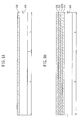
- FIGS. 1A to 1G illustrate the manufacture of an organic light emitting diode (OLED) display device according to an exemplary embodiment of the present invention.
- a substrate 100 including a thin film transistor region a and a capacitor region b is prepared, and a buffer layer 110 is formed on the substrate 100.
- the substrate 100 may be formed of glass or plastic, and the buffer layer 110 may be formed of a single insulating layer, such as one of a silicon oxide layer and a silicon nitride layer, or a stacked layer thereof, using a chemical vapor deposition (CVD) method or a physical vapor deposition (PVD) method.
- CVD chemical vapor deposition
- PVD physical vapor deposition
- the buffer layer 110 may function to prevent the diffusion of moisture or impurities from the substrate 100 or to adjust a heat transfer rate in crystallization to facilitate crystallization of a later-formed amorphous silicon layer.
- an amorphous silicon layer 120a is formed on the buffer layer 110. Then, a diffusion layer 123 and a metal catalyst layer 125 are formed on the amorphous silicon layer 120a.
- the amorphous silicon layer 120a may be formed by a CVD or PVD method. Further, when the amorphous silicon layer 120a is formed or after the amorphous silicon layer 120a is formed, a dehydrogenation process may be performed to lower the concentration of hydrogen.
- the diffusion layer 123 may be formed of a silicon nitride layer through which a metal catalyst to be formed in the following process can be diffused in an annealing process, and may be formed of a stacked layer of a silicon nitride layer and a silicon oxide layer.
- the diffusion layer 123 may be formed by a CVD or PVD method.
- the diffusion layer 123 may be formed to a thickness of 0.1nm (1 ⁇ ) to 200nm (2000 ⁇ ).
- the diffusion layer 123 may not sufficiently control the amount of metal catalyst diffused therethrough.
- the thickness of the diffusion layer 123 exceeds 200nm (2000 ⁇ )
- the amount of metal catalyst that diffuses to the amorphous silicon layer 120a is small, and thus it may be difficult to crystallize the amorphous silicon layer into a polysilicon layer.
- a metal catalyst is deposited on the diffusion layer 123 to form the metal catalyst layer 125.
- nickel (Ni) may be used as the metal catalyst.
- the metal catalyst layer 125 may be formed with an areal density of 1011 atoms/cm 2 to 1015 atoms/cm 2 on the diffusion layer 123. When the metal catalyst is formed with an areal density less than 1011 atoms/cm 2 , the amount of seeds that are crystallization nuclei is small, and thus the amorphous silicon layer may not be crystallized into a polysilicon layer using a super grain silicon (SGS) method.
- SGS super grain silicon
- the metal catalyst when the metal catalyst is formed with an areal density greater than 1015 atoms/cm 2 , the amount of metal catalyst diffused into the amorphous silicon layer is great, and thus grains of a resultant polysilicon layer are small. Furthermore, as the amount of remaining metal catalyst increases in the resultant polysilicon layer, characteristics of a semiconductor layer formed by patterning the polysilicon layer deteriorate.
- an annealing process is performed on the substrate 100 on which the buffer layer 110, the amorphous silicon layer 120a, the diffusion layer 123, and the metal catalyst layer 125 are formed to move at least a portion of the metal catalyst of the metal catalyst layer 125 to a surface of the amorphous silicon layer 120a. That is, only a small amount of metal catalyst diffuses through the diffusion layer 123 to the surface of the amorphous silicon layer 120a, and most of the metal catalyst does not reach the amorphous silicon layer 120a or pass through the diffusion layer 123.
- the amount of metal catalyst reaching the surface of the amorphous silicon layer 120a is determined depending on a diffusion blocking ability of the diffusion layer 123, and the diffusion blocking ability of the diffusion layer 123 is closely related to the thickness of the diffusion layer 123. For example, as the diffusion layer 123 becomes thicker, the amount of metal catalyst to be diffused is reduced, and thus the grain size is increased. Moreover, as the diffusion layer becomes thinner, the amount of metal catalyst to be diffused is increased, and thus the grain size is reduced.
- the annealing process may be performed at a temperature of 200°C to 900°C, for example, 350°C to 500°C for several seconds to several hours to diffuse the metal catalyst of the metal catalyst layer 125 to the amorphous silicon layer 120a.
- the annealing process may be performed using one of a furnace process, a rapid thermal annealing (RTA) process, an UV process, and a laser process (i.e., any of these processes).
- the diffusion layer 123 and the metal catalyst layer 125 are removed.
- the amorphous silicon layer 120a crystallized into the polysilicon layer is patterned to form a semiconductor layer 120.
- the semiconductor layer may be patterned using dry etching.
- the protrusion A remaining on the buffer layer 110 is formed in the same shape as a grain boundary that is formed by crystallizing the amorphous silicon layer into the polysilicon layer.
- the grain size of the semiconductor layer 120 formed of the polysilicon layer is great, the frequency of the protrusions A on the buffer layer is reduced, and when the grain size is small, the frequency of the protrusions A is increased.
- FIG. 2 is a photograph showing a surface of a buffer layer after a polysilicon layer crystallized by a metal catalyst is removed by dry etching. Referring to FIG. 2 , a protrusion formed to a thickness of up to 68nm (680 ⁇ ) is observed on the buffer layer 110, and a step difference of the protrusion may vary depending on crystallization condition and thickness of the removed polysilicon layer.
- a gate insulating layer 130 is formed on the surface of the substrate 100 on which the semiconductor layer 120 is formed.
- the gate insulating layer 130 is formed to cover at least a portion of the semiconductor layer 120 to insulate the semiconductor layer 120 from a later formed gate electrode or may be formed on the entire surface of the substrate 100 to cover the semiconductor layer 120.
- the gate insulating layer 130 may be formed of a silicon oxide layer, a silicon nitride layer or a combination thereof, and the protrusions A of the buffer layer causes the gate insulating layer 130 and the lower capacitor electrode 145 to have protrusions A in the same shape.
- a single layer of aluminum (Al) or an aluminum alloy, such as aluminum-neodymium (Al-Nd), or a multilayer in which an aluminum alloy is stacked on a chromium (Cr) or molybdenum (Mo) alloy is used to form a metal layer for a gate electrode (not shown).
- the metal layer for a gate electrode is etched using photolithography and etching to form a gate electrode 140 facing the semiconductor layer 120 in the thin film transistor region a at a predetermined region of the semiconductor layer 120, i.e., a channel region thereof, and a lower capacitor electrode 145 in the capacitor region b.
- the protrusions are formed on the lower capacitor electrode 145, and thus a surface area of the electrode is increased. As a result, the increased surface area causes a capacitance of the capacitor to be increased when the capacitor is completely formed.
- an interlayer insulating layer 150 is formed on the surface of the substrate 100 on which the gate electrode 140 and the lower capacitor electrode 145 are formed.
- the interlayer insulating layer 150 may be formed to cover the entire surface of the substrate 100, including the gate electrode 140 and the lower capacitor electrode 145, or may be formed to cover at least a portion of each of the gate electrode 140 and the lower capacitor electrode 145.
- a metal layer for source and drain electrodes (not shown) is formed on the surface of the interlayer insulating layer and then patterned, so that source and drain electrodes 160a and 160b disposed in the thin film transistor region a and electrically connected to the semiconductor layer 120, and an upper capacitor electrode 163 disposed on the capacitor region b and facing the lower electrode 145 are formed.
- the source and drain electrodes 160a and 160b are electrically connected to source and drain regions of the semiconductor layer 120 via through holes formed in the interlayer insulating layer 150 and the gate insulating layer 130. Further, because the lower capacitor electrode 145 and the upper capacitor electrode 163 follow the shape of the protrusions A of the buffer layer 110 and have an increased area, the capacitance of the resultant capacitor is increased.
- the interlayer insulating layer 150 may be formed of a silicon nitride layer, a silicon oxide layer, or a combination thereof.
- the source and drain electrodes 160a and 160b and the upper capacitor electrode 163 may be formed of one selected from the group consisting of molybdenum (Mo), chromium (Cr), tungsten (W), molybdenum-tungsten (MoW), aluminum (Al), aluminum-neodymium (Al-Nd), titanium (Ti), titanium nitride (TiN), copper (Cu), a Mo alloy, an Al alloy, and a Cu alloy.
- a first electrode 180 connected to one of the source and drain electrodes 160a and 160b of the thin film transistor region a is formed on the protection layer 170.
- the first electrode 180 is connected to the one of the source and drain electrodes 160a and 160b via a through hole formed in the protective layer 170.
- the first electrode 180 may be formed as an anode or a cathode.
- the anode may be formed of a transparent conductive layer made of ITO, IZO or ITZO; and when the first electrode 180 is formed as a cathode, the cathode may be formed of Mg, Ca, Al, Ag, Ba, or alloys thereof.
- a pixel defining layer 185 having an opening to at least partially expose the first electrode 180 is formed on the protective layer 170.
- the pixel defining layer 185 may also be formed to cover at least a portion of the first electrode 180.
- An organic layer 190, including a light emitting layer, is formed on the exposed first electrode 180.
- the organic layer 190 may comprise a hole injection layer, a hole transport layer, a hole blocking layer, an electron blocking layer, an electron injection layer, and an electron transport layer.
- a second electrode 195 is formed on the organic layer 190.
- MILC and MIC methods in which crystallization is performed using a metal catalyst can be used as the method of crystallizing the amorphous silicon layer, and the methods may be used alone or in combination.
- an amorphous silicon layer is crystallized using a metal catalyst to form a semiconductor layer formed of a polysilicon layer. Further, protrusions that are formed by residual metals remaining in the silicon layer upon crystallization on a buffer layer in the form of metal silicides cause a surface area of the buffer layer to be increased. As a result, an OLED display device may have a capacitor formed on the buffer layer whose capacitance is increased.
Landscapes
- Engineering & Computer Science (AREA)
- Microelectronics & Electronic Packaging (AREA)
- Physics & Mathematics (AREA)
- Geometry (AREA)
- Manufacturing & Machinery (AREA)
- Optics & Photonics (AREA)
- Thin Film Transistor (AREA)
- Electroluminescent Light Sources (AREA)
- Recrystallisation Techniques (AREA)
- Devices For Indicating Variable Information By Combining Individual Elements (AREA)
- Semiconductor Integrated Circuits (AREA)
- Electrodes Of Semiconductors (AREA)
Abstract
Description
- The present invention relates to an organic light emitting diode (OLED) display device and a method of fabricating the same, and more particularly, to an OLED display device including a capacitor whose capacitance is increased using a method of fabricating a polysilicon layer using a metal catalyst and a method of fabricating the same.
- In general, polysilicon is widely used as a semiconductor layer of a thin film transistor due to its high field effect mobility and applicability to high-speed operating circuits and complementary metal-oxide-semiconductor (CMOS) circuits. The thin film transistors having a polysilicon layer are generally used as active elements of active matrix liquid crystal displays (AMLCDs), and switching elements and driving elements of organic light emitting diodes (OLEDs).
- Here, methods of crystallizing an amorphous silicon layer into the polysilicon layer used for a thin film transistor include a solid phase crystallization (SPC) method, an excimer laser crystallization (ELC) method, a metal induced crystallization (MIC) method, and a metal induced lateral crystallization (MILC) method. In the SPC method, an amorphous silicon layer is annealed at a temperature of about 700°C or less, i.e., a transition temperature of a glass substrate of a display device for several hours to several tens of hours. In the ELC method, an excimer laser is irradiated on an amorphous silicon layer to locally heat the irradiated portion to a high temperature for a very short time period, so that the amorphous silicon layer is crystallized. In the MIC method, metals such as nickel, palladium, gold, aluminum, etc., are placed in contact with or injected into an amorphous silicon layer, so that the amorphous silicon layer is changed into a polysilicon layer, i.e., a phase change of the amorphous silicon is induced by the metal. In the MILC method, silicide, which is produced by reacting metal with silicon, is laterally and continuously diffused to sequentially induce crystallization of the amorphous silicon layer.
- However, the SPC method requires a long time, and the annealing process is performed at a high temperature for a long time, which may deform a substrate. Also, in the ELC method, a high-priced laser device is required, and protrusions may be formed on the polycrystalline surface such that interfacial characteristics between a semiconductor layer and a gate insulating layer may deteriorate.
- Currently, research into methods of crystallizing an amorphous silicon layer using a metal is actively progressing because crystallization can be achieved at a lower temperature and with less time than the SPC method. The methods of crystallizing an amorphous silicon layer using a metal include the MIC method, the MILC method, and a super grain silicon crystallization method.
- Meanwhile, in an OLED, capacitors are formed, and a capacitor having a high capacitance may be advantageous to the operation of the OLED. Thus, research into increasing the capacitance of the capacitor is required.
- Aspects of the present invention provide an organic light emitting diode (OLED) display device in which capacitance of a capacitor is increased by increasing a surface area of the capacitor in a simple manner and a method of fabricating the same.
- According to aspects of the present invention, an OLED display device includes: a substrate having a thin film transistor region and a capacitor region; a buffer layer disposed on the substrate; a patterned semiconductor layer disposed on the buffer layer in the thin film transistor region; a gate insulating layer disposed on the substrate to cover the patterned semiconductor layer; a gate electrode disposed on the gate insulating layer and facing a predetermined region of the patterned semiconductor layer; a lower capacitor electrode disposed on the gate insulating layer in the capacitor region; an interlayer insulating layer disposed on the substrate to cover the gate electrode and the lower capacitor electrode; source and drain electrodes disposed on the interlayer insulating layer and electrically connected to the patterned semiconductor layer, and an upper capacitor electrode disposed on the interlayer insulating layer and facing the lower capacitor electrode; a first electrode disposed on the interlayer insulating layer and electrically connected to one of the source and drain electrodes; an organic layer including a light emitting layer, the organic layer being disposed on the first electrode; and a second electrode disposed on the organic layer, wherein regions of each of the buffer layer, the gate insulating layer, the interlayer insulating layer, the lower capacitor electrode, and the upper capacitor electrode that are disposed in the capacitor region of the substrate have surfaces in which protrusions are formed, the protrusions following the shape of grain boundaries of the patterned semiconductor layer.
- According to aspects of the present invention, a method of fabricating an organic light emitting diode (OLED) display device includes: forming a substrate having a thin film transistor region and a capacitor region; forming a buffer layer on the substrate; forming an amorphous silicon layer on the buffer layer; forming a metal catalyst layer on the amorphous silicon layer; annealing the substrate to crystallize the amorphous silicon layer into a polysilicon layer; removing the metal catalyst layer; forming protrusions in the buffer layer while patterning the polysilicon layer to form a semiconductor layer in the thin film transistor region; forming a gate insulating layer on the substrate to cover the semiconductor layer; forming a gate electrode on the gate insulating layer and facing a predetermined region of the semiconductor layer; forming a lower capacitor electrode on the gate insulating layer in the capacitor region; forming an interlayer insulating layer on the substrate to cover the gate electrode and the lower capacitor electrode; forming source and drain electrodes on the interlayer insulating layer which are electrically connected to the semiconductor layer; forming an upper capacitor electrode on the interlayer insulating layer and facing the lower electrode; forming a first electrode on the interlayer insulating layer which is electrically connected to one of the source and drain regions of the semiconductor layer; forming an organic layer including a light emitting layer on the first electrode; and forming a second electrode on the organic layer.
- According to aspects of the present invention, an OLED display device includes: a substrate having a thin film transistor region and a capacitor region; a buffer layer disposed on the substrate, the buffer layer having protrusions in the capacitor region that extend therefrom away from the substrate; and a capacitor disposed on the buffer layer in the capacitor region, wherein the capacitor follows the shape of the protrusions of the buffer layer.
- According to aspects of the present invention, a method of manufacturing an organic light emitting diode (OLED) display device includes: forming a substrate having a thin film transistor region and a capacitor region; forming a buffer layer on the substrate; forming an amorphous silicon layer on the buffer layer; crystallizing the amorphous silicon layer to form a polysilicon layer having grain boundaries; forming protrusions in portions of the buffer layer adjacent to the grain boundaries of the polysilicon layer while patterning the polysilicon layer to form a semiconductor layer, the semiconductor layer being disposed in the thin film transistor region; forming a lower capacitor electrode on the gate insulating layer in the capacitor region, the lower capacitor electrode having protrusions corresponding to the protrusions of the buffer layer; forming an interlayer insulating layer on the substrate to cover at least the lower capacitor electrode, the interlayer insulating layer having protrusions corresponding to the protrusions of the lower capacitor electrode; and forming an upper capacitor electrode on the interlayer insulating layer and facing the lower electrode, the upper capacitor electrode having protrusions corresponding to the protrusions of the interlayer insulating layer.
- According to aspects of the present invention: a method of manufacturing an organic light emitting diode (OLED) display device includes: forming a buffer layer on a substrate; forming protrusions in portions of the buffer layer; forming a lower capacitor electrode on the gate insulating layer, the lower capacitor electrode having protrusions corresponding to the protrusions of the buffer layer; forming an interlayer insulating layer on the substrate to cover at least the lower capacitor electrode, the interlayer insulating layer having protrusions corresponding to the protrusions of the lower capacitor electrode; and forming an upper capacitor electrode on the interlayer insulating layer and facing the lower electrode, the upper capacitor electrode having protrusions corresponding to the protrusions of the interlayer insulating layer.
- Additional aspects and/or advantages of the invention will be set forth in part in the description which follows and, in part, will be obvious from the description, or may be learned by practice of the invention.
- These and/or other aspects and advantages of the invention will become apparent and more readily appreciated from the following description of the embodiments, taken in conjunction with the accompanying drawings of which:
-
FIGS. 1A to 1G illustrate manufacture of an organic light emitting diode (OLED) display device according to an exemplary embodiment of the present invention; and -
FIG. 2 is a photograph showing a surface of a buffer layer from which a polysilicon layer is removed according to an exemplary embodiment of the present invention. - Reference will now be made in detail to the present embodiments of the present invention, examples of which are illustrated in the accompanying drawings, wherein like reference numerals refer to the like elements throughout. The embodiments are described below in order to explain the present invention by referring to the figures. In the drawings, the sizes and proportions of layers/regions may be exaggerated, and like reference numerals refer to like elements. It will be understood that when an element such as a layer, film, region, or substrate is referred to as being "formed on" or "disposed on" another element, it can be disposed directly on the other element, or intervening elements may also be present. In contrast, when an element is referred to as being "formed directly on" or "disposed directly on" another element, there are no intervening elements present
-
FIGS. 1A to 1G illustrate the manufacture of an organic light emitting diode (OLED) display device according to an exemplary embodiment of the present invention. Referring toFIG. 1A , asubstrate 100 including a thin film transistor region a and a capacitor region b is prepared, and abuffer layer 110 is formed on thesubstrate 100. Thesubstrate 100 may be formed of glass or plastic, and thebuffer layer 110 may be formed of a single insulating layer, such as one of a silicon oxide layer and a silicon nitride layer, or a stacked layer thereof, using a chemical vapor deposition (CVD) method or a physical vapor deposition (PVD) method. - Here, the
buffer layer 110 may function to prevent the diffusion of moisture or impurities from thesubstrate 100 or to adjust a heat transfer rate in crystallization to facilitate crystallization of a later-formed amorphous silicon layer. - Next, referring to
FIG. 1B , anamorphous silicon layer 120a is formed on thebuffer layer 110. Then, adiffusion layer 123 and ametal catalyst layer 125 are formed on theamorphous silicon layer 120a. Here, theamorphous silicon layer 120a may be formed by a CVD or PVD method. Further, when theamorphous silicon layer 120a is formed or after theamorphous silicon layer 120a is formed, a dehydrogenation process may be performed to lower the concentration of hydrogen. Thediffusion layer 123 may be formed of a silicon nitride layer through which a metal catalyst to be formed in the following process can be diffused in an annealing process, and may be formed of a stacked layer of a silicon nitride layer and a silicon oxide layer. Thediffusion layer 123 may be formed by a CVD or PVD method. Here, thediffusion layer 123 may be formed to a thickness of 0.1nm (1Å) to 200nm (2000Å). When thediffusion layer 123 is formed to a thickness less than 0.1nm (1Å), thediffusion layer 123 may not sufficiently control the amount of metal catalyst diffused therethrough. When the thickness of thediffusion layer 123 exceeds 200nm (2000Å), the amount of metal catalyst that diffuses to theamorphous silicon layer 120a is small, and thus it may be difficult to crystallize the amorphous silicon layer into a polysilicon layer. - A metal catalyst is deposited on the
diffusion layer 123 to form themetal catalyst layer 125. Here, one selected from the group consisting of Ni, Pd, Ag, Au, Al, Sn, Sb, Cu, Tb, and Cd. For example, nickel (Ni) may be used as the metal catalyst. Here, themetal catalyst layer 125 may be formed with an areal density of 1011 atoms/cm2 to 1015 atoms/cm2 on thediffusion layer 123. When the metal catalyst is formed with an areal density less than 1011 atoms/cm2, the amount of seeds that are crystallization nuclei is small, and thus the amorphous silicon layer may not be crystallized into a polysilicon layer using a super grain silicon (SGS) method. Alternatively, when the metal catalyst is formed with an areal density greater than 1015 atoms/cm2, the amount of metal catalyst diffused into the amorphous silicon layer is great, and thus grains of a resultant polysilicon layer are small. Furthermore, as the amount of remaining metal catalyst increases in the resultant polysilicon layer, characteristics of a semiconductor layer formed by patterning the polysilicon layer deteriorate. - As described above, an annealing process is performed on the
substrate 100 on which thebuffer layer 110, theamorphous silicon layer 120a, thediffusion layer 123, and themetal catalyst layer 125 are formed to move at least a portion of the metal catalyst of themetal catalyst layer 125 to a surface of theamorphous silicon layer 120a. That is, only a small amount of metal catalyst diffuses through thediffusion layer 123 to the surface of theamorphous silicon layer 120a, and most of the metal catalyst does not reach theamorphous silicon layer 120a or pass through thediffusion layer 123. - Therefore, the amount of metal catalyst reaching the surface of the
amorphous silicon layer 120a is determined depending on a diffusion blocking ability of thediffusion layer 123, and the diffusion blocking ability of thediffusion layer 123 is closely related to the thickness of thediffusion layer 123. For example, as thediffusion layer 123 becomes thicker, the amount of metal catalyst to be diffused is reduced, and thus the grain size is increased. Moreover, as the diffusion layer becomes thinner, the amount of metal catalyst to be diffused is increased, and thus the grain size is reduced. - Here, the annealing process may be performed at a temperature of 200°C to 900°C, for example, 350°C to 500°C for several seconds to several hours to diffuse the metal catalyst of the
metal catalyst layer 125 to theamorphous silicon layer 120a. When the annealing process is performed at such a temperature for such a time period, deformation of a substrate caused by an excessive annealing process can be prevented to increase manufacturing yield and to reduce manufacturing costs. The annealing process may be performed using one of a furnace process, a rapid thermal annealing (RTA) process, an UV process, and a laser process (i.e., any of these processes). - After the
amorphous silicon layer 120a is crystallized into the polysilicon layer, thediffusion layer 123 and themetal catalyst layer 125 are removed. Referring toFIG. 1C , theamorphous silicon layer 120a crystallized into the polysilicon layer is patterned to form asemiconductor layer 120. Here, the semiconductor layer may be patterned using dry etching. - When the polysilicon layer is patterned into the
semiconductor layer 120 using dry etching, grain boundaries on which metal silicides of the polysilicon layer crystallized by the metal catalyst gather and a seed region are not completely removed from the surface of the etched buffer layer and remain as a protrusion A. Therefore, the protrusion A remaining on thebuffer layer 110 is formed in the same shape as a grain boundary that is formed by crystallizing the amorphous silicon layer into the polysilicon layer. In addition, when the grain size of thesemiconductor layer 120 formed of the polysilicon layer is great, the frequency of the protrusions A on the buffer layer is reduced, and when the grain size is small, the frequency of the protrusions A is increased. -
FIG. 2 is a photograph showing a surface of a buffer layer after a polysilicon layer crystallized by a metal catalyst is removed by dry etching. Referring toFIG. 2 , a protrusion formed to a thickness of up to 68nm (680Å) is observed on thebuffer layer 110, and a step difference of the protrusion may vary depending on crystallization condition and thickness of the removed polysilicon layer. - Referring to
FIG. 1D , agate insulating layer 130 is formed on the surface of thesubstrate 100 on which thesemiconductor layer 120 is formed. Thegate insulating layer 130 is formed to cover at least a portion of thesemiconductor layer 120 to insulate thesemiconductor layer 120 from a later formed gate electrode or may be formed on the entire surface of thesubstrate 100 to cover thesemiconductor layer 120. Thegate insulating layer 130 may be formed of a silicon oxide layer, a silicon nitride layer or a combination thereof, and the protrusions A of the buffer layer causes thegate insulating layer 130 and thelower capacitor electrode 145 to have protrusions A in the same shape. - Afterwards, a single layer of aluminum (Al) or an aluminum alloy, such as aluminum-neodymium (Al-Nd), or a multilayer in which an aluminum alloy is stacked on a chromium (Cr) or molybdenum (Mo) alloy is used to form a metal layer for a gate electrode (not shown). Then, the metal layer for a gate electrode is etched using photolithography and etching to form a
gate electrode 140 facing thesemiconductor layer 120 in the thin film transistor region a at a predetermined region of thesemiconductor layer 120, i.e., a channel region thereof, and alower capacitor electrode 145 in the capacitor region b. - Therefore, the protrusions are formed on the
lower capacitor electrode 145, and thus a surface area of the electrode is increased. As a result, the increased surface area causes a capacitance of the capacitor to be increased when the capacitor is completely formed. - Referring to
FIG. 1E , aninterlayer insulating layer 150 is formed on the surface of thesubstrate 100 on which thegate electrode 140 and thelower capacitor electrode 145 are formed. The interlayer insulatinglayer 150 may be formed to cover the entire surface of thesubstrate 100, including thegate electrode 140 and thelower capacitor electrode 145, or may be formed to cover at least a portion of each of thegate electrode 140 and thelower capacitor electrode 145. Afterwards, a metal layer for source and drain electrodes (not shown) is formed on the surface of the interlayer insulating layer and then patterned, so that source anddrain electrodes semiconductor layer 120, and anupper capacitor electrode 163 disposed on the capacitor region b and facing thelower electrode 145 are formed. The source anddrain electrodes semiconductor layer 120 via through holes formed in theinterlayer insulating layer 150 and thegate insulating layer 130. Further, because thelower capacitor electrode 145 and theupper capacitor electrode 163 follow the shape of the protrusions A of thebuffer layer 110 and have an increased area, the capacitance of the resultant capacitor is increased. - The interlayer insulating
layer 150 may be formed of a silicon nitride layer, a silicon oxide layer, or a combination thereof. Also, the source anddrain electrodes upper capacitor electrode 163 may be formed of one selected from the group consisting of molybdenum (Mo), chromium (Cr), tungsten (W), molybdenum-tungsten (MoW), aluminum (Al), aluminum-neodymium (Al-Nd), titanium (Ti), titanium nitride (TiN), copper (Cu), a Mo alloy, an Al alloy, and a Cu alloy. - Afterwards, referring to
FIG. 1F , after aprotection layer 170 is formed on the entire surface of the substrate, afirst electrode 180 connected to one of the source anddrain electrodes protection layer 170. Thefirst electrode 180 is connected to the one of the source anddrain electrodes protective layer 170. - The
first electrode 180 may be formed as an anode or a cathode. When thefirst electrode 180 is formed as an anode, the anode may be formed of a transparent conductive layer made of ITO, IZO or ITZO; and when thefirst electrode 180 is formed as a cathode, the cathode may be formed of Mg, Ca, Al, Ag, Ba, or alloys thereof. - Referring to
FIG. 1G , apixel defining layer 185 having an opening to at least partially expose thefirst electrode 180 is formed on theprotective layer 170. Thepixel defining layer 185 may also be formed to cover at least a portion of thefirst electrode 180. Anorganic layer 190, including a light emitting layer, is formed on the exposedfirst electrode 180. Theorganic layer 190 may comprise a hole injection layer, a hole transport layer, a hole blocking layer, an electron blocking layer, an electron injection layer, and an electron transport layer. Asecond electrode 195 is formed on theorganic layer 190. As a result, the OLED display device according to an example embodiment of the present invention is completed. - While a polysilicon layer crystallized using a SGS method is described, MILC and MIC methods in which crystallization is performed using a metal catalyst can be used as the method of crystallizing the amorphous silicon layer, and the methods may be used alone or in combination.
- According to aspects of the present invention, an amorphous silicon layer is crystallized using a metal catalyst to form a semiconductor layer formed of a polysilicon layer. Further, protrusions that are formed by residual metals remaining in the silicon layer upon crystallization on a buffer layer in the form of metal silicides cause a surface area of the buffer layer to be increased. As a result, an OLED display device may have a capacitor formed on the buffer layer whose capacitance is increased.
- Although a few embodiments of the present invention have been shown and described, it would be appreciated by those skilled in the art that changes may be made in these embodiments without departing from the principles of the invention, the scope of which is defined in the claims.
Claims (15)
- An organic light emitting diode OLED display device, comprising:a substrate (100) having a thin film transistor region (a) and a capacitor region (b);a buffer layer (110) disposed on the substrate, the buffer layer having protrusions in the capacitor region (b) that extend away from the substrate; anda capacitor (145, 150, 163) disposed on the buffer layer in the capacitor region,wherein the capacitor follows the shape of the protrusions of the buffer layer.
- The OLED display device of claim 1, wherein the protrusions extend to a height of up to 68nm from the surface of the buffer layer (110).
- The OLED display device of claim 1 or 2, further comprising:a semiconductor layer (120) disposed on the buffer layer (110) in the thin film transistor region, wherein the protrusions are formed in the buffer layer except for the portion of the buffer layer on which the semiconductor layer is formed.
- The OLED display device of any one of the preceding claims, wherein the capacitor comprises:a first capacitor electrode (145) disposed on the buffer layer;an interlayer insulating layer (150) disposed on the first electrode; anda second capacitor electrode (163) disposed on the interlayer insulating layer,wherein the first capacitor electrode, the second capacitor electrode and the interlayer insulating layer follow the shape of the protrusions of the buffer layer.
- The OLED display device of any one of the preceding claims, further comprising a gate insulating layer (130) disposed on the buffer layer between the buffer layer and the capacitor.
- The OLED display device of any one of the preceding claims, wherein the buffer layer has a higher concentration of metal silicides near the protrusions.
- The OLED display device of claim 3, wherein the protrusions follow the shape of grain boundaries of the semiconductor layer.
- The OLED display device of claim 5, further comprising a gate electrode on the gate insulating layer, wherein the gate electrode is formed of one of a single layer of aluminum (Al), a single layer of an aluminum (Al) alloy, a multilayer of a chromium (Cr) alloy and an aluminum (Al) alloy, and a multilayer of a molybdenum (Mo) alloy and an aluminum (Al) alloy.
- The OLED display device of claim 8, wherein the first capacitor electrode is formed of the same material as the gate electrode, and/or wherein the buffer layer is formed of a silicon oxide layer, a silicon nitride layer, or a stacked layer thereof, and/or wherein the second capacitor electrode is formed of the same material as the source and drain electrodes, and/or wherein the second capacitor electrode is formed of one selected from the group consisting of molybdenum (Mo), chromium (Cr), tungsten (W), molybdenum-tungsten (MoW), aluminum (Al), aluminum-neodymium (Al-Nd), titanium (Ti), titanium nitride (TiN), copper (Cu), a Mo alloy, an Al alloy, and a Cu alloy.
- The OLED display device of claim 3, wherein, when the grain size of the semiconductor layer is decreased, the buffer layer has more protrusions and/or
wherein the protrusions are formed where seeds of crystallization of the semiconductor layer were disposed before the semiconductor layer was patterned. - A method of fabricating an organic light emitting diode (OLED) display device, the method comprising:forming a substrate (100) having a thin film transistor region and a capacitor region;forming a buffer layer (110) on the substrate;forming protrusions in the buffer layer; andforming a capacitor (145, 150, 163) on the buffer layer in the capacitor region,wherein the capacitor follows the shape of the protrusions of the buffer layer.
- The method of claim 11, wherein the step of forming protrusions in the buffer layer comprises:forming an amorphous silicon layer (120a) on the buffer layer;forming a metal catalyst layer (125) on the amorphous silicon layer;annealing the substrate to crystallize the amorphous silicon layer into a polysilicon layer;removing the metal catalyst layer (125); andpatterning the polysilicon layer to form a semiconductor layer (120) in the thin film transistor region.
- The method of claim 12, further comprising:forming a gate insulating layer (130) on the substrate to cover the semiconductor layer;forming a gate electrode (140) on the gate insulating layer to face a predetermined region of the semiconductor layer;forming a first capacitor electrode (145) on the gate insulating layer in the capacitor region;forming an interlayer insulating layer (150) on the substrate to cover the gate electrode and the first capacitor electrode;forming source and drain electrodes (160a, 160b) on the interlayer insulating layer which are electrically connected to the semiconductor layer;forming a second capacitor electrode (163) on the interlayer insulating layer to face the first capacitor electrode;forming a first electrode (180) on the interlayer insulating layer, the first electrode being electrically connected to one of the source and drain regions of the semiconductor layer;forming an organic layer (190) on the first electrode, the organic layer including a light emitting layer; andforming a second electrode (195) on the organic layer.
- The method of claim 12 or 13, further comprising:forming a diffusion layer (123) on the amorphous silicon layer (120a) and forming the metal catalyst layer (125) on the diffusion layer,wherein the annealing is performed after the forming of the metal catalyst layer.
- The method of claim 13, wherein the first capacitor electrode and the gate electrode are formed by simultaneous patterning and/or wherein the second capacitor electrode and the source and drain electrodes are formed by simultaneous patterning.
Applications Claiming Priority (1)
| Application Number | Priority Date | Filing Date | Title |
|---|---|---|---|
| KR1020090018200A KR101041141B1 (en) | 2009-03-03 | 2009-03-03 | Organic light emitting display device and manufacturing method |
Publications (3)
| Publication Number | Publication Date |
|---|---|
| EP2226845A2 true EP2226845A2 (en) | 2010-09-08 |
| EP2226845A3 EP2226845A3 (en) | 2014-04-02 |
| EP2226845B1 EP2226845B1 (en) | 2018-04-11 |
Family
ID=42235340
Family Applications (1)
| Application Number | Title | Priority Date | Filing Date |
|---|---|---|---|
| EP10154502.8A Active EP2226845B1 (en) | 2009-03-03 | 2010-02-24 | Method of fabricating an organic light emitting diode display device |
Country Status (5)
| Country | Link |
|---|---|
| US (2) | US8409887B2 (en) |
| EP (1) | EP2226845B1 (en) |
| JP (1) | JP5399298B2 (en) |
| KR (1) | KR101041141B1 (en) |
| CN (1) | CN101826548B (en) |
Families Citing this family (27)
| Publication number | Priority date | Publication date | Assignee | Title |
|---|---|---|---|---|
| KR20120042143A (en) * | 2010-10-22 | 2012-05-03 | 삼성모바일디스플레이주식회사 | Organinc light emitting display device and manufacturing method for the same |
| KR101781532B1 (en) * | 2011-03-14 | 2017-10-24 | 삼성디스플레이 주식회사 | An organic light emitting display device and the manufacturing method thereof |
| JP6019329B2 (en) * | 2011-03-31 | 2016-11-02 | 株式会社Joled | Display device and electronic device |
| KR101847910B1 (en) * | 2011-05-26 | 2018-04-13 | 삼성디스플레이 주식회사 | Method for adjusting the distance of bumps in pixel region and Method for manufacturing display device using the same |
| KR101860859B1 (en) | 2011-06-13 | 2018-05-25 | 삼성디스플레이 주식회사 | Manufacturing method of thin film transistor, the thin film transistor manufactured by the same, manufacturing method of organic light emitting apparatus and the organic light emitting apparatus manufactured by the same |
| KR20120138168A (en) * | 2011-06-14 | 2012-12-24 | 삼성디스플레이 주식회사 | Display device and method for manufacturing the same |
| KR101901361B1 (en) * | 2011-12-02 | 2018-09-27 | 삼성디스플레이 주식회사 | Method for formation of crystalline silicon layer and method for formation of thin film transistor using the same |
| KR101903445B1 (en) * | 2012-01-10 | 2018-10-05 | 삼성디스플레이 주식회사 | Semiconductor device and method for manufacturing thereof |
| KR101887082B1 (en) * | 2012-04-05 | 2018-08-13 | 한국전자통신연구원 | Organic light emitting diode device and fabrication method thereof |
| US8658444B2 (en) * | 2012-05-16 | 2014-02-25 | International Business Machines Corporation | Semiconductor active matrix on buried insulator |
| KR20150043890A (en) * | 2013-10-15 | 2015-04-23 | 삼성디스플레이 주식회사 | Organic light emitting diode display |
| KR102253966B1 (en) * | 2013-12-09 | 2021-05-18 | 엘지디스플레이 주식회사 | Organic light emitting diode display device, fabricating and inspecting method thereof |
| KR102257978B1 (en) * | 2014-03-17 | 2021-05-31 | 삼성디스플레이 주식회사 | Display divece and method for preparing the same |
| CN105789319B (en) * | 2014-12-26 | 2020-05-01 | 昆山国显光电有限公司 | Thin film transistor and preparation method thereof |
| KR102441558B1 (en) * | 2015-04-07 | 2022-09-08 | 삼성디스플레이 주식회사 | Organic light emitting display device and manufacturing method thereof |
| KR102378360B1 (en) * | 2015-05-12 | 2022-03-25 | 삼성디스플레이 주식회사 | Organic light-emitting display |
| CN105097835A (en) * | 2015-07-07 | 2015-11-25 | 合肥鑫晟光电科技有限公司 | Array substrate, manufacturing method thereof, display panel and display device |
| KR102716398B1 (en) * | 2016-06-17 | 2024-10-11 | 삼성디스플레이 주식회사 | Organic light emitting diode display and method for manufacturing organic light emitting diode display |
| KR102859906B1 (en) * | 2016-10-06 | 2025-09-16 | 삼성디스플레이 주식회사 | Display device |
| KR102531126B1 (en) | 2017-06-14 | 2023-05-11 | 삼성디스플레이 주식회사 | Unit pixel and organic light emitting display device including the same |
| KR102448095B1 (en) * | 2017-09-08 | 2022-09-29 | 삼성디스플레이 주식회사 | Display device, manufacturing method of display device, and electrode building method |
| KR102740999B1 (en) | 2018-10-31 | 2024-12-12 | 삼성디스플레이 주식회사 | Display apparatus and method of manufacturing the same |
| KR102711211B1 (en) * | 2018-11-02 | 2024-09-27 | 엘지디스플레이 주식회사 | Transistor, panel, and electronic device |
| CN110752222B (en) | 2019-10-31 | 2021-11-26 | 厦门天马微电子有限公司 | Display panel, manufacturing method thereof and display device |
| KR20220060007A (en) * | 2020-11-02 | 2022-05-11 | 삼성디스플레이 주식회사 | Light emitting element ink, display device and method for manufacturing of the same |
| CN113690253A (en) * | 2021-08-13 | 2021-11-23 | Tcl华星光电技术有限公司 | Array substrate, manufacturing method of array substrate and display panel |
| CN116322151A (en) * | 2021-12-20 | 2023-06-23 | 广东聚华印刷显示技术有限公司 | Capacitor component of array substrate, array substrate and manufacturing method, and display panel |
Family Cites Families (87)
| Publication number | Priority date | Publication date | Assignee | Title |
|---|---|---|---|---|
| JPS6333868A (en) | 1986-07-28 | 1988-02-13 | Nec Corp | Manufacture of mis field-effect transistor |
| JPS63304668A (en) | 1987-06-03 | 1988-12-12 | Fujitsu Ltd | Manufacture of insulated-gate transistor |
| JP2617950B2 (en) | 1987-10-16 | 1997-06-11 | 松下電器産業株式会社 | Manufacturing method of liquid crystal display device |
| JPH04135161A (en) | 1990-09-21 | 1992-05-08 | Ietatsu Ono | Polishing method and device thereof |
| JP3076119B2 (en) | 1991-12-25 | 2000-08-14 | 株式会社日立製作所 | Manufacturing method of liquid crystal display device |
| EP0589049B1 (en) | 1992-03-25 | 2000-01-12 | Kanegafuchi Chemical Industry Co., Ltd. | Thin polysilicon film and production thereof |
| JP3139154B2 (en) * | 1992-08-19 | 2001-02-26 | セイコーエプソン株式会社 | Liquid crystal device and method of manufacturing the same |
| JPH0669515A (en) | 1992-08-19 | 1994-03-11 | Fujitsu Ltd | Semiconductor memory device |
| JP3107941B2 (en) | 1993-03-05 | 2000-11-13 | 株式会社半導体エネルギー研究所 | Thin film transistor and manufacturing method thereof |
| JPH0713196A (en) * | 1993-06-21 | 1995-01-17 | Toshiba Corp | Active matrix liquid crystal display |
| KR100294026B1 (en) | 1993-06-24 | 2001-09-17 | 야마자끼 순페이 | Electro-optical device |
| US7081938B1 (en) | 1993-12-03 | 2006-07-25 | Semiconductor Energy Laboratory Co., Ltd. | Electro-optical device and method for manufacturing the same |
| JPH0845850A (en) | 1994-07-27 | 1996-02-16 | Oki Electric Ind Co Ltd | Growth method of doped polycrystalline semiconductor thin film |
| JP3295679B2 (en) | 1995-08-04 | 2002-06-24 | 株式会社半導体エネルギー研究所 | Method for manufacturing semiconductor device |
| JP3143591B2 (en) * | 1995-09-14 | 2001-03-07 | キヤノン株式会社 | Display device |
| JP3476320B2 (en) | 1996-02-23 | 2003-12-10 | 株式会社半導体エネルギー研究所 | Semiconductor thin film and method for manufacturing the same, semiconductor device and method for manufacturing the same |
| TW317643B (en) | 1996-02-23 | 1997-10-11 | Handotai Energy Kenkyusho Kk | |
| KR100205523B1 (en) | 1996-04-08 | 1999-07-01 | 구자홍 | Thin film transistor and its fabrication method |
| JPH1174536A (en) | 1997-01-09 | 1999-03-16 | Sanyo Electric Co Ltd | Method for manufacturing semiconductor device |
| JP2000031488A (en) | 1997-08-26 | 2000-01-28 | Semiconductor Energy Lab Co Ltd | Semiconductor device and manufacturing method thereof |
| KR20000055877A (en) | 1999-02-10 | 2000-09-15 | 장진 | Polycrystalline silicon containing nickel |
| KR100317638B1 (en) | 1999-03-19 | 2001-12-22 | 구본준, 론 위라하디락사 | Polysilicon-thin film transister device and A method of fabricating the same |
| US6878968B1 (en) | 1999-05-10 | 2005-04-12 | Semiconductor Energy Laboratory Co., Ltd. | Semiconductor device |
| JP3706527B2 (en) | 1999-06-30 | 2005-10-12 | Hoya株式会社 | Electron beam drawing mask blanks, electron beam drawing mask, and method of manufacturing electron beam drawing mask |
| JP3715848B2 (en) | 1999-09-22 | 2005-11-16 | シャープ株式会社 | Manufacturing method of semiconductor device |
| US6294442B1 (en) | 1999-12-10 | 2001-09-25 | National Semiconductor Corporation | Method for the formation of a polysilicon layer with a controlled, small silicon grain size during semiconductor device fabrication |
| JP4200618B2 (en) | 1999-12-27 | 2008-12-24 | ソニー株式会社 | Semiconductor film forming method and thin film semiconductor device manufacturing method |
| GB2358081B (en) | 2000-01-07 | 2004-02-18 | Seiko Epson Corp | A thin-film transistor and a method for maufacturing thereof |
| KR100450595B1 (en) | 2000-02-09 | 2004-09-30 | 히다찌 케이블 리미티드 | Crystalline silicon semiconductor device and method for fabricating same |
| JP4769997B2 (en) | 2000-04-06 | 2011-09-07 | ソニー株式会社 | THIN FILM TRANSISTOR AND ITS MANUFACTURING METHOD, LIQUID CRYSTAL DISPLAY DEVICE, LIQUID CRYSTAL DISPLAY DEVICE MANUFACTURING METHOD, ORGANIC EL DEVICE, AND ORGANIC EL DEVICE MANUFACTURING METHOD |
| JP2001337348A (en) | 2000-05-30 | 2001-12-07 | Toshiba Corp | Array substrate and method of manufacturing the same |
| KR100387122B1 (en) | 2000-09-15 | 2003-06-12 | 피티플러스(주) | Fabrication Method of Poly-Si Thin Film Transistor Having Back Bias Effects |
| JP4267266B2 (en) * | 2001-07-10 | 2009-05-27 | 株式会社半導体エネルギー研究所 | Method for manufacturing semiconductor device |
| JP2003060209A (en) | 2001-08-08 | 2003-02-28 | Sharp Corp | Semiconductor device and method of manufacturing the same |
| JP2003100629A (en) | 2001-09-19 | 2003-04-04 | Sharp Corp | Semiconductor device and manufacturing method thereof |
| JP4135347B2 (en) | 2001-10-02 | 2008-08-20 | 株式会社日立製作所 | Method for producing polysilicon film |
| JP2003188098A (en) | 2001-12-13 | 2003-07-04 | Sharp Corp | Semiconductor device and method of manufacturing the same |
| US6933527B2 (en) | 2001-12-28 | 2005-08-23 | Semiconductor Energy Laboratory Co., Ltd. | Semiconductor device and semiconductor device production system |
| TW536716B (en) * | 2002-07-04 | 2003-06-11 | Ind Tech Res Inst | Capacitor structure of low temperature polysilicon |
| JP4092261B2 (en) | 2002-08-02 | 2008-05-28 | 三星エスディアイ株式会社 | Manufacturing method of substrate and manufacturing method of organic electroluminescence element |
| KR100603284B1 (en) * | 2002-10-22 | 2006-07-20 | 삼성에스디아이 주식회사 | Electroluminescent Display Panels with Increased Capacitance |
| KR20040036761A (en) | 2002-10-24 | 2004-05-03 | 엘지전자 주식회사 | Method of silicon deposition using of hdp-cvd |
| KR100470274B1 (en) | 2002-11-08 | 2005-02-05 | 진 장 | Method of phase transition of amorphous material using a cap layer |
| JP4115252B2 (en) | 2002-11-08 | 2008-07-09 | シャープ株式会社 | Semiconductor film and manufacturing method thereof, and semiconductor device and manufacturing method thereof |
| TWI305681B (en) | 2002-11-22 | 2009-01-21 | Toppoly Optoelectronics Corp | Method for fabricating thin film transistor array and driving circuits |
| JP3904512B2 (en) | 2002-12-24 | 2007-04-11 | シャープ株式会社 | SEMICONDUCTOR DEVICE, ITS MANUFACTURING METHOD, AND ELECTRONIC DEVICE PROVIDED WITH SEMICONDUCTOR DEVICE |
| JP4059095B2 (en) | 2003-02-07 | 2008-03-12 | セイコーエプソン株式会社 | Complementary thin film transistor circuit, electro-optical device, electronic equipment |
| TW200520229A (en) | 2003-12-03 | 2005-06-16 | Toppoly Optoelectronics Corp | Thin film transistor of multi-gate structure and its manufacturing method |
| US7238963B2 (en) | 2003-04-28 | 2007-07-03 | Tpo Displays Corp. | Self-aligned LDD thin-film transistor and method of fabricating the same |
| KR20040098958A (en) | 2003-05-16 | 2004-11-26 | 삼성에스디아이 주식회사 | Thin film transistor and method for fabricating the same |
| US7358165B2 (en) | 2003-07-31 | 2008-04-15 | Semiconductor Energy Laboratory Co., Ltd | Semiconductor device and method for manufacturing semiconductor device |
| JP4578877B2 (en) | 2003-07-31 | 2010-11-10 | 株式会社半導体エネルギー研究所 | Semiconductor device and manufacturing method thereof |
| KR100623228B1 (en) | 2003-11-27 | 2006-09-18 | 삼성에스디아이 주식회사 | A thin film transistor, an organic light emitting display device having the thin film transistor, and a manufacturing method of the thin film transistor |
| KR100579188B1 (en) | 2004-02-12 | 2006-05-11 | 삼성에스디아이 주식회사 | Thin Film Transistor with LED Structure |
| US8114719B2 (en) | 2004-06-03 | 2012-02-14 | Semiconductor Energy Laboratory Co., Ltd. | Memory device and manufacturing method of the same |
| KR100600874B1 (en) | 2004-06-09 | 2006-07-14 | 삼성에스디아이 주식회사 | Thin film transistor and its manufacturing method |
| KR100626007B1 (en) | 2004-06-30 | 2006-09-20 | 삼성에스디아이 주식회사 | A thin film transistor, a method of manufacturing the thin film transistor, a flat panel display device having a thin film transistor, and a method of manufacturing a flat panel display device |
| KR100611659B1 (en) | 2004-07-07 | 2006-08-10 | 삼성에스디아이 주식회사 | Thin film transistor and its manufacturing method |
| KR100611764B1 (en) | 2004-08-20 | 2006-08-10 | 삼성에스디아이 주식회사 | Manufacturing Method of Thin Film Transistor |
| KR100611766B1 (en) | 2004-08-24 | 2006-08-10 | 삼성에스디아이 주식회사 | Method of manufacturing thin film transistor |
| US7416928B2 (en) * | 2004-09-08 | 2008-08-26 | Semiconductor Energy Laboratory Co., Ltd. | Manufacturing method of semiconductor device |
| KR100628989B1 (en) | 2004-09-17 | 2006-09-27 | 진 장 | Crystallization Method of Amorphous Silicon Thin Film |
| KR20060026776A (en) | 2004-09-21 | 2006-03-24 | 삼성에스디아이 주식회사 | Organic electroluminescent device and manufacturing method thereof |
| KR100689316B1 (en) | 2004-10-29 | 2007-03-08 | 엘지.필립스 엘시디 주식회사 | Organic light emitting diode device and manufacturing method thereof |
| KR100669789B1 (en) * | 2004-11-26 | 2007-01-16 | 삼성에스디아이 주식회사 | Flat panel display device |
| JP5073482B2 (en) | 2005-03-31 | 2012-11-14 | 東京エレクトロン株式会社 | Silicon oxide film manufacturing method, control program thereof, storage medium, and plasma processing apparatus |
| US7341907B2 (en) | 2005-04-05 | 2008-03-11 | Applied Materials, Inc. | Single wafer thermal CVD processes for hemispherical grained silicon and nano-crystalline grain-sized polysilicon |
| US7652291B2 (en) | 2005-05-28 | 2010-01-26 | Samsung Mobile Display Co., Ltd. | Flat panel display |
| TWI401802B (en) | 2005-06-30 | 2013-07-11 | 三星電子股份有限公司 | Thin film transistor plate and method of manufacturing same |
| JP2007027202A (en) * | 2005-07-12 | 2007-02-01 | Sharp Corp | Display device manufacturing method and display device |
| JP2007035812A (en) * | 2005-07-26 | 2007-02-08 | Mitsubishi Electric Corp | Polycrystalline silicon film manufacturing method and thin film transistor |
| JP4815600B2 (en) | 2005-09-06 | 2011-11-16 | 株式会社テラセミコン | Polycrystalline silicon thin film manufacturing method and manufacturing apparatus thereof |
| KR100778781B1 (en) | 2005-12-16 | 2007-11-27 | 주식회사 테라세미콘 | Polycrystalline silicon thin film manufacturing method and apparatus for manufacturing same |
| US20080258186A1 (en) | 2005-12-19 | 2008-10-23 | Nxp B.V. | Source and Drain Formation in Silicon on Insulator Device |
| KR20070076860A (en) * | 2006-01-20 | 2007-07-25 | 삼성전자주식회사 | Organic light emitting display and manufacturing method |
| TWI296855B (en) | 2006-03-07 | 2008-05-11 | Au Optronics Corp | Thin film transistor and manufacturing method thereof |
| KR100770269B1 (en) | 2006-05-18 | 2007-10-25 | 삼성에스디아이 주식회사 | Method of manufacturing thin film transistor |
| KR101270168B1 (en) | 2006-09-19 | 2013-05-31 | 삼성전자주식회사 | Organic electro-luminescent display and fabrication method thereof |
| KR100770266B1 (en) * | 2006-11-10 | 2007-10-25 | 삼성에스디아이 주식회사 | Organic light emitting display device and manufacturing method |
| KR100864884B1 (en) | 2006-12-28 | 2008-10-22 | 삼성에스디아이 주식회사 | Thin film transistor, manufacturing method thereof and organic light emitting display device having same |
| KR100864883B1 (en) | 2006-12-28 | 2008-10-22 | 삼성에스디아이 주식회사 | A thin film transistor, a manufacturing method thereof, and an organic light emitting display device having the same. |
| KR100839735B1 (en) | 2006-12-29 | 2008-06-19 | 삼성에스디아이 주식회사 | Transistor, manufacturing method thereof and flat panel display device having same |
| KR100889626B1 (en) * | 2007-08-22 | 2009-03-20 | 삼성모바일디스플레이주식회사 | Thin film transistor, manufacturing method thereof, organic light emitting display device having same, and manufacturing method thereof |
| JP2009059940A (en) | 2007-08-31 | 2009-03-19 | Sharp Corp | THIN FILM TRANSISTOR, METHOD FOR MANUFACTURING THIN FILM TRANSISTOR, AND ELECTRONIC DEVICE |
| KR20080086967A (en) | 2008-08-28 | 2008-09-29 | 삼성에스디아이 주식회사 | Thin film transistor and organic light emitting display device having same |
| KR101049799B1 (en) | 2009-03-03 | 2011-07-15 | 삼성모바일디스플레이주식회사 | Thin film transistor, manufacturing method thereof and organic light emitting display device comprising same |
| KR101015849B1 (en) | 2009-03-03 | 2011-02-23 | 삼성모바일디스플레이주식회사 | Thin film transistor, manufacturing method thereof and organic light emitting display device comprising same |
-
2009
- 2009-03-03 KR KR1020090018200A patent/KR101041141B1/en not_active Expired - Fee Related
-
2010
- 2010-02-24 EP EP10154502.8A patent/EP2226845B1/en active Active
- 2010-02-26 CN CN2010101239740A patent/CN101826548B/en active Active
- 2010-02-26 US US12/713,846 patent/US8409887B2/en active Active
- 2010-03-01 JP JP2010044020A patent/JP5399298B2/en active Active
-
2013
- 2013-03-15 US US13/841,121 patent/US9035311B2/en active Active
Non-Patent Citations (1)
| Title |
|---|
| None |
Also Published As
| Publication number | Publication date |
|---|---|
| KR101041141B1 (en) | 2011-06-13 |
| US20100224881A1 (en) | 2010-09-09 |
| CN101826548B (en) | 2012-10-24 |
| CN101826548A (en) | 2010-09-08 |
| KR20100099617A (en) | 2010-09-13 |
| US20130228760A1 (en) | 2013-09-05 |
| JP5399298B2 (en) | 2014-01-29 |
| US8409887B2 (en) | 2013-04-02 |
| JP2010206200A (en) | 2010-09-16 |
| US9035311B2 (en) | 2015-05-19 |
| EP2226845B1 (en) | 2018-04-11 |
| EP2226845A3 (en) | 2014-04-02 |
Similar Documents
| Publication | Publication Date | Title |
|---|---|---|
| EP2226845B1 (en) | Method of fabricating an organic light emitting diode display device | |
| JP5090253B2 (en) | Method for manufacturing polycrystalline silicon layer, thin film transistor formed using the same, method for manufacturing the same, and organic light emitting display device including the same | |
| US8513669B2 (en) | Thin film transistor including metal or metal silicide structure in contact with semiconductor layer and organic light emitting diode display device having the thin film transistor | |
| KR100889627B1 (en) | Thin film transistor, manufacturing method thereof, and organic light emitting display device having same | |
| KR100848341B1 (en) | Thin film transistor, manufacturing method thereof, and organic light emitting display device comprising the same | |
| EP2226833B1 (en) | Method of fabricating a thin film transistor | |
| US8507914B2 (en) | Method of fabricating polysilicon, thin film transistor, method of fabricating the thin film transistor, and organic light emitting diode display device including the thin film transistor | |
| CN101211985A (en) | Thin film transistor, manufacturing method thereof, and organic light emitting diode display device | |
| KR101049799B1 (en) | Thin film transistor, manufacturing method thereof and organic light emitting display device comprising same | |
| US8294158B2 (en) | Thin film transistor, method of fabricating the same, and organic light emitting diode display device including the thin film transistor | |
| US8278716B2 (en) | Method of fabricating polysilicon, thin film transistor, method of fabricating the thin film transistor, and organic light emitting diode display device including the thin film transistor |
Legal Events
| Date | Code | Title | Description |
|---|---|---|---|
| PUAI | Public reference made under article 153(3) epc to a published international application that has entered the european phase |
Free format text: ORIGINAL CODE: 0009012 |
|
| 17P | Request for examination filed |
Effective date: 20100224 |
|
| AK | Designated contracting states |
Kind code of ref document: A2 Designated state(s): AT BE BG CH CY CZ DE DK EE ES FI FR GB GR HR HU IE IS IT LI LT LU LV MC MK MT NL NO PL PT RO SE SI SK SM TR |
|
| AX | Request for extension of the european patent |
Extension state: AL BA RS |
|
| RAP1 | Party data changed (applicant data changed or rights of an application transferred) |
Owner name: SAMSUNG DISPLAY CO., LTD. |
|
| PUAL | Search report despatched |
Free format text: ORIGINAL CODE: 0009013 |
|
| AK | Designated contracting states |
Kind code of ref document: A3 Designated state(s): AT BE BG CH CY CZ DE DK EE ES FI FR GB GR HR HU IE IS IT LI LT LU LV MC MK MT NL NO PL PT RO SE SI SK SM TR |
|
| AX | Request for extension of the european patent |
Extension state: AL BA RS |
|
| RIC1 | Information provided on ipc code assigned before grant |
Ipc: H01L 27/32 20060101AFI20140226BHEP |
|
| RAP1 | Party data changed (applicant data changed or rights of an application transferred) |
Owner name: SAMSUNG DISPLAY CO., LTD. |
|
| STAA | Information on the status of an ep patent application or granted ep patent |
Free format text: STATUS: EXAMINATION IS IN PROGRESS |
|
| 17Q | First examination report despatched |
Effective date: 20170127 |
|
| GRAP | Despatch of communication of intention to grant a patent |
Free format text: ORIGINAL CODE: EPIDOSNIGR1 |
|
| STAA | Information on the status of an ep patent application or granted ep patent |
Free format text: STATUS: GRANT OF PATENT IS INTENDED |
|
| INTG | Intention to grant announced |
Effective date: 20171025 |
|
| GRAS | Grant fee paid |
Free format text: ORIGINAL CODE: EPIDOSNIGR3 |
|
| GRAA | (expected) grant |
Free format text: ORIGINAL CODE: 0009210 |
|
| STAA | Information on the status of an ep patent application or granted ep patent |
Free format text: STATUS: THE PATENT HAS BEEN GRANTED |
|
| AK | Designated contracting states |
Kind code of ref document: B1 Designated state(s): AT BE BG CH CY CZ DE DK EE ES FI FR GB GR HR HU IE IS IT LI LT LU LV MC MK MT NL NO PL PT RO SE SI SK SM TR |
|
| REG | Reference to a national code |
Ref country code: GB Ref legal event code: FG4D |
|
| REG | Reference to a national code |
Ref country code: CH Ref legal event code: EP |
|
| REG | Reference to a national code |
Ref country code: AT Ref legal event code: REF Ref document number: 988881 Country of ref document: AT Kind code of ref document: T Effective date: 20180415 |
|
| REG | Reference to a national code |
Ref country code: IE Ref legal event code: FG4D |
|
| REG | Reference to a national code |
Ref country code: DE Ref legal event code: R096 Ref document number: 602010049797 Country of ref document: DE |
|
| REG | Reference to a national code |
Ref country code: NL Ref legal event code: MP Effective date: 20180411 |
|
| REG | Reference to a national code |
Ref country code: LT Ref legal event code: MG4D |
|
| PG25 | Lapsed in a contracting state [announced via postgrant information from national office to epo] |
Ref country code: NL Free format text: LAPSE BECAUSE OF FAILURE TO SUBMIT A TRANSLATION OF THE DESCRIPTION OR TO PAY THE FEE WITHIN THE PRESCRIBED TIME-LIMIT Effective date: 20180411 |
|
| PG25 | Lapsed in a contracting state [announced via postgrant information from national office to epo] |
Ref country code: SE Free format text: LAPSE BECAUSE OF FAILURE TO SUBMIT A TRANSLATION OF THE DESCRIPTION OR TO PAY THE FEE WITHIN THE PRESCRIBED TIME-LIMIT Effective date: 20180411 Ref country code: LT Free format text: LAPSE BECAUSE OF FAILURE TO SUBMIT A TRANSLATION OF THE DESCRIPTION OR TO PAY THE FEE WITHIN THE PRESCRIBED TIME-LIMIT Effective date: 20180411 Ref country code: ES Free format text: LAPSE BECAUSE OF FAILURE TO SUBMIT A TRANSLATION OF THE DESCRIPTION OR TO PAY THE FEE WITHIN THE PRESCRIBED TIME-LIMIT Effective date: 20180411 Ref country code: NO Free format text: LAPSE BECAUSE OF FAILURE TO SUBMIT A TRANSLATION OF THE DESCRIPTION OR TO PAY THE FEE WITHIN THE PRESCRIBED TIME-LIMIT Effective date: 20180711 Ref country code: PL Free format text: LAPSE BECAUSE OF FAILURE TO SUBMIT A TRANSLATION OF THE DESCRIPTION OR TO PAY THE FEE WITHIN THE PRESCRIBED TIME-LIMIT Effective date: 20180411 Ref country code: FI Free format text: LAPSE BECAUSE OF FAILURE TO SUBMIT A TRANSLATION OF THE DESCRIPTION OR TO PAY THE FEE WITHIN THE PRESCRIBED TIME-LIMIT Effective date: 20180411 Ref country code: BG Free format text: LAPSE BECAUSE OF FAILURE TO SUBMIT A TRANSLATION OF THE DESCRIPTION OR TO PAY THE FEE WITHIN THE PRESCRIBED TIME-LIMIT Effective date: 20180711 |
|
| PG25 | Lapsed in a contracting state [announced via postgrant information from national office to epo] |
Ref country code: HR Free format text: LAPSE BECAUSE OF FAILURE TO SUBMIT A TRANSLATION OF THE DESCRIPTION OR TO PAY THE FEE WITHIN THE PRESCRIBED TIME-LIMIT Effective date: 20180411 Ref country code: LV Free format text: LAPSE BECAUSE OF FAILURE TO SUBMIT A TRANSLATION OF THE DESCRIPTION OR TO PAY THE FEE WITHIN THE PRESCRIBED TIME-LIMIT Effective date: 20180411 Ref country code: GR Free format text: LAPSE BECAUSE OF FAILURE TO SUBMIT A TRANSLATION OF THE DESCRIPTION OR TO PAY THE FEE WITHIN THE PRESCRIBED TIME-LIMIT Effective date: 20180712 |
|
| REG | Reference to a national code |
Ref country code: AT Ref legal event code: MK05 Ref document number: 988881 Country of ref document: AT Kind code of ref document: T Effective date: 20180411 |
|
| PG25 | Lapsed in a contracting state [announced via postgrant information from national office to epo] |
Ref country code: PT Free format text: LAPSE BECAUSE OF FAILURE TO SUBMIT A TRANSLATION OF THE DESCRIPTION OR TO PAY THE FEE WITHIN THE PRESCRIBED TIME-LIMIT Effective date: 20180813 |
|
| REG | Reference to a national code |
Ref country code: DE Ref legal event code: R097 Ref document number: 602010049797 Country of ref document: DE |
|
| PG25 | Lapsed in a contracting state [announced via postgrant information from national office to epo] |
Ref country code: EE Free format text: LAPSE BECAUSE OF FAILURE TO SUBMIT A TRANSLATION OF THE DESCRIPTION OR TO PAY THE FEE WITHIN THE PRESCRIBED TIME-LIMIT Effective date: 20180411 Ref country code: SK Free format text: LAPSE BECAUSE OF FAILURE TO SUBMIT A TRANSLATION OF THE DESCRIPTION OR TO PAY THE FEE WITHIN THE PRESCRIBED TIME-LIMIT Effective date: 20180411 Ref country code: CZ Free format text: LAPSE BECAUSE OF FAILURE TO SUBMIT A TRANSLATION OF THE DESCRIPTION OR TO PAY THE FEE WITHIN THE PRESCRIBED TIME-LIMIT Effective date: 20180411 Ref country code: RO Free format text: LAPSE BECAUSE OF FAILURE TO SUBMIT A TRANSLATION OF THE DESCRIPTION OR TO PAY THE FEE WITHIN THE PRESCRIBED TIME-LIMIT Effective date: 20180411 Ref country code: AT Free format text: LAPSE BECAUSE OF FAILURE TO SUBMIT A TRANSLATION OF THE DESCRIPTION OR TO PAY THE FEE WITHIN THE PRESCRIBED TIME-LIMIT Effective date: 20180411 Ref country code: DK Free format text: LAPSE BECAUSE OF FAILURE TO SUBMIT A TRANSLATION OF THE DESCRIPTION OR TO PAY THE FEE WITHIN THE PRESCRIBED TIME-LIMIT Effective date: 20180411 |
|
| PLBE | No opposition filed within time limit |
Free format text: ORIGINAL CODE: 0009261 |
|
| STAA | Information on the status of an ep patent application or granted ep patent |
Free format text: STATUS: NO OPPOSITION FILED WITHIN TIME LIMIT |
|
| PG25 | Lapsed in a contracting state [announced via postgrant information from national office to epo] |
Ref country code: SM Free format text: LAPSE BECAUSE OF FAILURE TO SUBMIT A TRANSLATION OF THE DESCRIPTION OR TO PAY THE FEE WITHIN THE PRESCRIBED TIME-LIMIT Effective date: 20180411 Ref country code: IT Free format text: LAPSE BECAUSE OF FAILURE TO SUBMIT A TRANSLATION OF THE DESCRIPTION OR TO PAY THE FEE WITHIN THE PRESCRIBED TIME-LIMIT Effective date: 20180411 |
|
| 26N | No opposition filed |
Effective date: 20190114 |
|
| PG25 | Lapsed in a contracting state [announced via postgrant information from national office to epo] |
Ref country code: SI Free format text: LAPSE BECAUSE OF FAILURE TO SUBMIT A TRANSLATION OF THE DESCRIPTION OR TO PAY THE FEE WITHIN THE PRESCRIBED TIME-LIMIT Effective date: 20180411 |
|
| REG | Reference to a national code |
Ref country code: CH Ref legal event code: PL |
|
| PG25 | Lapsed in a contracting state [announced via postgrant information from national office to epo] |
Ref country code: LU Free format text: LAPSE BECAUSE OF NON-PAYMENT OF DUE FEES Effective date: 20190224 Ref country code: MC Free format text: LAPSE BECAUSE OF FAILURE TO SUBMIT A TRANSLATION OF THE DESCRIPTION OR TO PAY THE FEE WITHIN THE PRESCRIBED TIME-LIMIT Effective date: 20180411 |
|
| REG | Reference to a national code |
Ref country code: BE Ref legal event code: MM Effective date: 20190228 |
|
| REG | Reference to a national code |
Ref country code: IE Ref legal event code: MM4A |
|
| PG25 | Lapsed in a contracting state [announced via postgrant information from national office to epo] |
Ref country code: LI Free format text: LAPSE BECAUSE OF NON-PAYMENT OF DUE FEES Effective date: 20190228 Ref country code: CH Free format text: LAPSE BECAUSE OF NON-PAYMENT OF DUE FEES Effective date: 20190228 |
|
| PG25 | Lapsed in a contracting state [announced via postgrant information from national office to epo] |
Ref country code: IE Free format text: LAPSE BECAUSE OF NON-PAYMENT OF DUE FEES Effective date: 20190224 |
|
| PG25 | Lapsed in a contracting state [announced via postgrant information from national office to epo] |
Ref country code: BE Free format text: LAPSE BECAUSE OF NON-PAYMENT OF DUE FEES Effective date: 20190228 |
|
| PG25 | Lapsed in a contracting state [announced via postgrant information from national office to epo] |
Ref country code: TR Free format text: LAPSE BECAUSE OF FAILURE TO SUBMIT A TRANSLATION OF THE DESCRIPTION OR TO PAY THE FEE WITHIN THE PRESCRIBED TIME-LIMIT Effective date: 20180411 |
|
| PG25 | Lapsed in a contracting state [announced via postgrant information from national office to epo] |
Ref country code: MT Free format text: LAPSE BECAUSE OF NON-PAYMENT OF DUE FEES Effective date: 20190224 |
|
| PG25 | Lapsed in a contracting state [announced via postgrant information from national office to epo] |
Ref country code: CY Free format text: LAPSE BECAUSE OF FAILURE TO SUBMIT A TRANSLATION OF THE DESCRIPTION OR TO PAY THE FEE WITHIN THE PRESCRIBED TIME-LIMIT Effective date: 20180411 |
|
| PG25 | Lapsed in a contracting state [announced via postgrant information from national office to epo] |
Ref country code: IS Free format text: LAPSE BECAUSE OF FAILURE TO SUBMIT A TRANSLATION OF THE DESCRIPTION OR TO PAY THE FEE WITHIN THE PRESCRIBED TIME-LIMIT Effective date: 20180811 |
|
| PG25 | Lapsed in a contracting state [announced via postgrant information from national office to epo] |
Ref country code: HU Free format text: LAPSE BECAUSE OF FAILURE TO SUBMIT A TRANSLATION OF THE DESCRIPTION OR TO PAY THE FEE WITHIN THE PRESCRIBED TIME-LIMIT; INVALID AB INITIO Effective date: 20100224 |
|
| PG25 | Lapsed in a contracting state [announced via postgrant information from national office to epo] |
Ref country code: MK Free format text: LAPSE BECAUSE OF FAILURE TO SUBMIT A TRANSLATION OF THE DESCRIPTION OR TO PAY THE FEE WITHIN THE PRESCRIBED TIME-LIMIT Effective date: 20180411 |
|
| REG | Reference to a national code |
Ref country code: DE Ref legal event code: R079 Ref document number: 602010049797 Country of ref document: DE Free format text: PREVIOUS MAIN CLASS: H01L0027320000 Ipc: H10K0059000000 |
|
| P01 | Opt-out of the competence of the unified patent court (upc) registered |
Effective date: 20230515 |
|
| PGFP | Annual fee paid to national office [announced via postgrant information from national office to epo] |
Ref country code: GB Payment date: 20260122 Year of fee payment: 17 |
|
| PGFP | Annual fee paid to national office [announced via postgrant information from national office to epo] |
Ref country code: DE Payment date: 20260120 Year of fee payment: 17 |
|
| PGFP | Annual fee paid to national office [announced via postgrant information from national office to epo] |
Ref country code: FR Payment date: 20260121 Year of fee payment: 17 |