EP2219239B1 - Halbleiterleuchtdiode - Google Patents
Halbleiterleuchtdiode Download PDFInfo
- Publication number
- EP2219239B1 EP2219239B1 EP20100153505 EP10153505A EP2219239B1 EP 2219239 B1 EP2219239 B1 EP 2219239B1 EP 20100153505 EP20100153505 EP 20100153505 EP 10153505 A EP10153505 A EP 10153505A EP 2219239 B1 EP2219239 B1 EP 2219239B1
- Authority
- EP
- European Patent Office
- Prior art keywords
- layer
- light emitting
- roughness
- emitting diode
- semiconductor layer
- Prior art date
- Legal status (The legal status is an assumption and is not a legal conclusion. Google has not performed a legal analysis and makes no representation as to the accuracy of the status listed.)
- Active
Links
Images


Classifications
-
- H—ELECTRICITY
- H10—SEMICONDUCTOR DEVICES; ELECTRIC SOLID-STATE DEVICES NOT OTHERWISE PROVIDED FOR
- H10H—INORGANIC LIGHT-EMITTING SEMICONDUCTOR DEVICES HAVING POTENTIAL BARRIERS
- H10H20/00—Individual inorganic light-emitting semiconductor devices having potential barriers, e.g. light-emitting diodes [LED]
- H10H20/80—Constructional details
- H10H20/84—Coatings, e.g. passivation layers or antireflective coatings
-
- H—ELECTRICITY
- H10—SEMICONDUCTOR DEVICES; ELECTRIC SOLID-STATE DEVICES NOT OTHERWISE PROVIDED FOR
- H10H—INORGANIC LIGHT-EMITTING SEMICONDUCTOR DEVICES HAVING POTENTIAL BARRIERS
- H10H20/00—Individual inorganic light-emitting semiconductor devices having potential barriers, e.g. light-emitting diodes [LED]
- H10H20/01—Manufacture or treatment
- H10H20/011—Manufacture or treatment of bodies, e.g. forming semiconductor layers
- H10H20/018—Bonding of wafers
-
- H—ELECTRICITY
- H10—SEMICONDUCTOR DEVICES; ELECTRIC SOLID-STATE DEVICES NOT OTHERWISE PROVIDED FOR
- H10H—INORGANIC LIGHT-EMITTING SEMICONDUCTOR DEVICES HAVING POTENTIAL BARRIERS
- H10H20/00—Individual inorganic light-emitting semiconductor devices having potential barriers, e.g. light-emitting diodes [LED]
- H10H20/80—Constructional details
- H10H20/882—Scattering means
Definitions
- the embodiment relates to a semiconductor light emitting diode and a method of manufacturing the same.
- Groups III-V nitride semiconductors have been extensively used as main materials for light emitting devices, such as a light emitting diode (LED) or a laser diode (LD), due to the physical and chemical characteristics thereof.
- the groups III-V nitride semiconductors include a semiconductor material having a compositional formula of In x Al y Ga 1-x-y N (0 ⁇ x ⁇ 1, 0 ⁇ y ⁇ 1, and 0 ⁇ x+y ⁇ 1).
- the LED is a semiconductor device, which transmits/receives signals by converting an electric signal into infrared ray or light using the characteristics of compound semiconductors.
- the LED is also used as a light source.
- the LED or LD using the nitride semiconductor material is mainly used for the light emitting device to provide the light.
- the LED or the LD is used as a light source for various products, such as a keypad light emitting part of a cellular phone, an electric signboard, and an illumination device.
- US 2004/0104390 A1 discloses a nitride semiconductor LED according to the preamble of claim 1.
- the embodiment of the present invention defined by claim 1 provides a semiconductor light emitting diode and a method of manufacturing the same, capable of improving a light extraction angle in a lateral direction of a light emitting structure.
- the embodiment provides a semiconductor light emitting diode and a method of manufacturing the same, capable of improving a light extraction angle of light emitted in a lateral direction of a light emitting structure by forming roughness on an outer surface of the light emitting structure.
- the present invention provides a semiconductor light emitting diode according to the claims.
- a method of manufacturing a semiconductor light emitting diode includes forming a light emitting structure using a plurality of compound semiconductor layers; forming a roughness on an outer surface of the light emitting structure; forming a channel layer on an outer portion of a top surface of the light emitting structure and the roughness; forming a second electrode layer on the channel layer and the light emitting structure, and exposing an outer portion of the channel layer by removing an outer peripheral portion of the light emitting structure through a mesa etching.
- the embodiment can improve light emitting efficiency in the lateral direction.
- the embodiment can improve a light extraction angle of a light emitting diode.
- the embodiment can improve external light emitting efficiency.
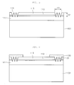
- FIG. 1 is a side sectional view showing a semiconductor light emitting diode according to the embodiment of the present invention.
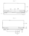
- FIGS. 2 to 9 are views showing the procedure for manufacturing a semiconductor light emitting diode according to the embodiment.
- each layer shown in the drawings can be exaggerated, omitted or schematically drawn for the purpose of convenience or clarity.
- the size of elements does not utterly reflect an actual size.
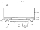
- FIG. 1 is a side sectional view showing a semiconductor light emitting diode according to the embodiment of the present invention.
- the semiconductor light emitting diode 100 includes a light emitting structure 110, a channel layer having a roughness 125, a second electrode layer 130 and a conductive support member 140.
- the light emitting structure 110 includes a first conductive semiconductor layer 111, an active layer 113, and a second conductive semiconductor layer 115.
- the active layer 113 is interposed between the first and second conductive semiconductor layers 111 and 115.
- the first conductive semiconductor layer 111 may include at least one semiconductor layer doped with a first conductive dopant.
- the first conductive semiconductor layer 111 may include a group III-V compound semiconductor.
- the first conductive semiconductor layer 111 may be formed of at least one selected from the group consisting of GaN, InN, AlN, InGaN, AlGaN, InAlGaN and AlInN.
- the first conductive semiconductor layer 111 is an N type semiconductor layer
- the first conductive dopant is an N type dopant.
- the N type dopant can be selected from the group V elements.
- a first electrode layer 119 is disposed on the top surface of the first conductive semiconductor layer 111.
- the roughness can be formed on a part or a whole area of the top surface of the first conductive semiconductor layer 111.
- the active layer 113 is formed below the first conductive semiconductor layer 111.
- the active layer 113 has a single quantum well structure or a multiple quantum well (MQW) structure.
- the active layer 113 may have a stack structure including a well layer and a barrier layer, which are made from group III-V compound semiconductor material.
- the active layer 113 has a stack structure of InGaN well/GaN barrier layers or AlGaN well/GaN barrier layers.
- the active layer 113 is made from material having band gap energy according to wavelength of light to be emitted. For instance, in the case of blue light having wavelength of 460 to 470 nm, the active layer 113 has a single quantum well structure or a multiple quantum well structure including the InGaN well/GaN barrier layers.
- the active layer 113 may include material capable of providing light of visible ray band, such as blue light, red light and green light.
- a conductive clad layer may be formed on and/or under the active layer 113.
- the conductive clad layer may include an AlGaN layer.
- the second conductive semiconductor layer 115 is disposed below the active layer 113.
- the second conductive semiconductor layer 115 includes at least one semiconductor layer doped with the second conductive dopant.
- the second conductive semiconductor layer 115 may include a group III-V compound semiconductor.
- the second conductive layer 115 may be formed of at least one selected from the group consisting of GaN, InN, AlN, InGaN, AlGaN, InAlGaN and AlInN.
- the second conductive semiconductor layer 115 is a P type semiconductor layer
- the second conductive dopant is a P type dopant.
- the P type dopant can be selected from the group III elements.
- a third conductive semiconductor layer (not shown) can be formed on the second conductive semiconductor layer 115. If the first conductive semiconductor layer 111 is a P type semiconductor layer, the second conductive semiconductor layer 115 is an N type semiconductor layer. The third conductive semiconductor layer may be doped with the first conductive dopant.
- the light emitting structure 110 may include one of an N-P junction structure, a P-N junction structure, an N-P-N junction structure, and a P-N-P junction structure.
- the channel layer 120 and the second electrode 130 are aligned below the second conductive semiconductor layer 115.
- An inner portion of the channel layer 120 is disposed below the second conductive semiconductor layer 115 along an outer peripheral portion of the second conductive semiconductor layer 115.
- An outer portion of the channel layer 120 extends out of the second conductive semiconductor layer 115 so that the channel layer 120 is exposed at an outer peripheral region 118 of the light emitting structure 110.
- the channel layer 120 may be formed of conductive material or insulating material having light transmittive property.
- the channel layer 120 is prepared in the form of a frame and is disposed between the second conductive semiconductor layer 115 and the second electrode layer 130.
- the channel layer 120 may include conductive material selected from the group consisting of ITO, IZO, IZTO, IAZO, IGZO, IGTO, AZO and ATO.
- the channel layer 120 may include insulating material selected from the group consisting of SiO 2 , SiO x , SiO x N y , Si 3 N 4 , Al 2 O 3 and TiO 2 .
- the channel layer 120 may improve adhesive property relative to the second conductive semiconductor layer 115.
- the channel layer 120 Since the channel layer 120 is exposed through an isolation etching process when the mesa etching is performed later, the channel layer 120 is referred to as an isolation layer. In addition, since the channel layer 120 serves as an etching stopper during the isolation etching process, the channel layer 120 may be referred to as an etching stop layer.
- the roughness 125 is formed on the channel layer 120.
- the roughness 125 may have various sectional shapes, such as a conical shape, a triangular shape, a polygonal shape, a convex lens shape or a random shape.
- the roughness 125 refers to a non-planar or non-even surface.
- the roughness 125 may include a protruding structure formed through a patterning process.
- the roughness 125 may include a plurality of protrusions, which are regularly or irregularly protruded, and can be inclined with respect to a vertical line.
- the roughness 125 is made from the insulating material, the roughness 125 can make contact with the outer surface of the light emitting structure 110. In addition, if the roughness 125 is made from the conductive material, the roughness 125 is spaced apart from the light emitting structure by a predetermined distance.
- the roughness 125 of the channel layer 120 may be provided corresponding to one side, two opposite sides or all sides of the light emitting structure 110. In addition, the roughness 125 of the channel layer 120 may be provided corresponding to both sides (for instance, left and right sides and/or front and rear sides) of light emitting structure 110 with asymmetrical size and shape.
- the roughness 125 of the channel layer 120 may protrude by a predetermined height D2.
- the predetermined height D2 is 50 nm or above.
- the top surface of the roughness 125 is located higher than the top surface of the active layer 113.
- the channel layer 120 and the roughness 125 may vary the incident angle of light, which is emitted in the lateral direction of the light emitting structure 110 or reflected from the second electrode layer 130, thereby improving the external light emitting efficiency.
- the second electrode layer 130 is formed below the second conductive semiconductor layer 115 and the channel layer 120.
- the second electrode layer 130 may be formed of at least one layer including at least one selected from the group consisting of Ag, Ni, Al, Rh, Pd, Ir, Ru, Mg, Zn, Pt, Au, Hf and combination thereof.
- An ohmic layer (not shown) having a predetermined pattern can be formed between the second electrode layer 130 and the second conductive semiconductor layer 115.
- the ohmic layer may have a matrix pattern, a cross pattern, a polygonal pattern or a circular pattern.
- the ohmic layer may be formed of at least one selected from the group consisting of ITO (indium tin oxide), IZO (indium zinc oxide), IZTO (indium zinc tin oxide), IAZO (indium aluminum zinc oxide), IGZO (indium gallium zinc oxide), IGTO (indium gallium tin oxide), AZO (aluminum zinc oxide) and ATO (antimony tin oxide).
- the conductive support member 140 is formed below the second electrode layer 130.
- the conductive support member 140 may be formed of material selected from the group consisting of copper, gold, and carrier wafers (for instance, Si, Ge, GaAs, ZnO, and SiC).
- FIGS. 2 to 9 are views showing the procedure for manufacturing the semiconductor light emitting diode according to the embodiment.
- the first conductive semiconductor layer 111 is formed on a substrate 101, and the active layer 113 is formed on the first conductive semiconductor layer 111.
- the second conductive semiconductor layer 115 is formed on the active layer 113.
- the substrate 101 may be formed of material selected from the group consisting of Al 2 O 3 , GaN, SiC, ZnO, Si, GaP, InP and GaAs.
- a predetermined concave-convex pattern can be formed on the substrate 101.
- Another semiconductor layer, such as a buffer layer and/or an undoped semiconductor layer, can be formed on the substrate 101 without limitation.
- the second conductive semiconductor layer 115 is a P type semiconductor layer. In contrast, if the first conductive semiconductor layer 111 is a P type semiconductor layer, the second conductive semiconductor layer 115 is an N type semiconductor layer.
- Another semiconductor layer such as a buffer layer and/or an undoped semiconductor layer, can be formed between the substrate 101 and the first conductive semiconductor layer 111. This semiconductor layer is removed or separated after the thin film has been grown.
- a roughness 116 is formed on an outer portion of the top surface of the second conductive semiconductor layer 115.
- the roughness 116 is formed along an upper outer portion of the second conductive semiconductor layer 115 by a predetermined depth D2.
- the predetermined depth D2 is 500 nm or above.
- a predetermined portion of the first conductive semiconductor layer 111 may be exposed due to the roughness 116.
- width D1 of the roughness 116 in the second conductive semiconductor layer 115 must be set such that the roughness function can be realized without exerting an influence upon the light emitting area.
- width D1 of the roughness 116 is in the range of 100 nm (1000 ⁇ ) to 500 nm (5000 ⁇ ).
- the roughness 116 refers to a non-planar surface.
- the roughness 116 may include a protruding structure formed through a patterning process.
- the roughness 116 can be formed by dry-etching the second conductive semiconductor layer 115.
- the dry-etching is performed in a state in which a mask pattern having a predetermined shape has been formed on the second conductive semiconductor layer 115.
- the dry-etching can be performed in a state in which an irregular layer has been formed on the second conductive semiconductor layer 115.
- the irregular layer may include a photoresist layer or a metal layer.
- the roughness 116 may have various sectional shapes, such as a reverse-conical shape, a polygonal shape, a concave lens shape or a random shape.
- a plurality of roughness 116 can be regularly or irregularly provided.
- the roughness 116 is formed at a boundary area between individual chips.
- the roughness 116 may be provided corresponding to one top side, two opposite top sides or all top sides of the light emitting structure 110 without limitation.
- the roughness 116 may be provided corresponding to both sides (for instance, left and right sides and/or front and rear sides) of light emitting structure 110 with asymmetrical size and shape.
- the channel layer 120 is formed on an outer peripheral portion of the top surface of the second conductive semiconductor layer 115.
- the channel layer 120 may be formed of material selected from the group consisting of ITO, IZO, IZTO, IAZO, IGZO, IGTO, AZO, ATO, SiO 2 , SiO x , SiO x N y , Si 3 N 4 , Al 2 O 3 , and TiO 2.
- the channel layer 120 is formed with the roughness 125 having the shape corresponding to the shape of the roughness 116.
- the roughness 125 is formed on the outer peripheral portion of the second conductive semiconductor layer 115, the active layer 113 and the first conductive semiconductor layer 111.
- the channel layer 120 is prepared in the form of a frame and is disposed on an outer peripheral portion of the second conductive semiconductor layer 115 of an individual chip.
- the channel layer 120 and the roughness 125 may be formed by using the same material or two different materials.
- the second electrode layer 130 is formed on the channel layer 130 and the second conductive semiconductor layer 115, and the conductive support member 140 is formed on the second electrode layer 130.
- the second electrode layer 130 and the conductive support member 140 are conductive layers that serve as a second electrode.
- An ohmic layer (not shown) having a predetermined pattern can be formed between the second conductive semiconductor layer 115 and the second electrode layer 130.
- the second electrode layer 130 may be formed of at least one layer including at least one selected from the group consisting of Ag, Ni, Al, Rh, Pd, Ir, Ru, Mg, Zn, Pt, Au, Hf and combination thereof.
- the conductive support member 140 may be formed with a predetermined thickness by using material selected from the group consisting of copper, gold, and carrier wafers (for instance, Si, Ge, GaAs, ZnO, and SiC).
- the substrate 101 disposed below the first conductive semiconductor layer 111 is removed through the laser lift off (LLO) scheme. That is, if the laser having a predetermined wavelength band is irradiated onto the substrate 101, a thermal energy is concentrated on the boundary surface between the substrate 101 and the first conductive semiconductor layer 111, so that the substrate 101 is separated from the first conductive semiconductor layer 111.
- the substrate 101 can be removed through another scheme. For instance, if another semiconductor layer, such as a buffer layer, exists between the substrate 101 and the first conductive semiconductor layer 111, wet etchant is injected into the buffer layer to remove the buffer layer, thereby removing the substrate 101.
- the bottom surface of the first conductive semiconductor layer 111 is polished through the ICP/RIE (inductively coupled plasma/reactive ion etching) scheme.
- a mesa etching is performed to expose an outer lower portion of the channel layer 120 at the chip boundary region.
- the mesa etching may be the dry etching or the wet etching.
- the channel layer 120 includes conductive material, the light emitting efficiency can be improved due to the ohmic characteristic of the channel layer 120. If the channel layer 120 includes insulating material, the gap between the second electrode 130 and the second conductive semiconductor layer 115 can be widened.
- the roughness 125 is exposed along the outer portion of the light emitting structure 110 at the outer lower portion of the channel layer 120.
- the roughness 125 protrudes such that the roughness 125 can be exposed in the stack direction of the light emitting structure 110.
- the first electrode layer 119 having a predetermined pattern can be formed below the first conductive semiconductor layer 111.
- the roughness can be formed on the bottom surface of the first conductive semiconductor layer 111.
- a dicing process is performed to provide individual chips.
- the roughness 125 protrudes along the outer peripheral region 118 of the light emitting structure 110 in the stack direction of the light emitting structure 110 at the outer lower portion of the channel layer 120.
- the roughness 125 can vary the incident angle of the light emitted from the light emitting structure 110 or reflected from the second electrode layer 130 formed below the channel layer 120, thereby improving the external light emitting efficiency.
- the embodiment is applicable in the light emitting device for supplying light.
Landscapes
- Led Devices (AREA)
Claims (9)
- Lichtemittierende Halbleiterdiode (100), umfassend:eine lichtemittierende Struktur (110), die eine erste leitfähige Halbleiterschicht (111), eine aktive Schicht (113) unter der ersten leitfähigen Halbleiterschicht und eine zweite leitfähige Halbleiterschicht (115) unter der aktiven Schicht aufweist;eine Isolationsschicht (120) unter der lichtemittierenden Struktur, bei der ein Innenabschnitt der Isolationsschicht entlang eines äußeren peripheren Abschnitts (118) der lichtemittierenden Struktur (110) angeordnet ist und sich ein äußerer Abschnitt der Isolationsschicht aus der lichtemittierenden Struktur heraus erstreckt, wobei die Isolationsschicht (120) eine Rauheit (125) aufweist, die auf einer oberen Oberfläche an einem Außenabschnitt der Isolationsschicht (120) ausgebildet ist; undeine zweite Elektrodenschicht (130) unter der lichtemittierenden Struktur (110);dadurch gekennzeichnet, dass eine obere Oberfläche der Rauheit (125) höher ist als eine obere Oberfläche der aktiven Schicht (113).
- Lichtemittierende Halbleiterdiode nach Anspruch 1, wobei das Material der Isolationsschicht (120) wenigstens ein Material umfasst, das innerhalb der Gruppe bestehend aus ITO, IZO, IZTO, IAZO, IGZO, IGTO, AZO, ATO, SiO2, SiOx, SiOxNy, Si3N4, Al2O3 und TiO2 ausgewählt ist.
- Lichtemittierende Halbleiterdiode nach Anspruch 1 oder Anspruch 2, die weiterhin ein leitfähiges Stützelement (140) unter der zweiten Elektrodenschicht (130) umfasst.
- Lichtemittierende Halbleiterdiode nach einem der vorangehenden Ansprüche, die weiterhin eine erste Elektrode (119) auf der lichtemittierenden Struktur umfasst.
- Lichtemittierende Halbleiterdiode nach Anspruch 1, wobei die Rauheit (125) von der Isolationsschicht (120) um wenigstens 50 nm vorsteht.
- Lichtemittierende Halbleiterdiode nach Anspruch 1, wobei die Rauheit (125) eine konische Form, eine polygonale Form und/oder eine konvexe Form umfasst.
- Lichtemittierende Halbleiterdiode nach einem der vorangehenden Ansprüche, wobei die Isolationsschicht (120) ein lichtdurchlässiges leitfähiges Material umfasst.
- Lichtemittierende Halbleiterdiode nach einem der vorangehenden Ansprüche, wobei die Isolationsschicht (120) ein Isoliermaterial umfasst.
- Lichtemittierende Halbleiterdiode nach einem der vorangehenden Ansprüche, wobei die zweite Elektrodenschicht (130) wenigstens eine Schicht aufweist, deren Material wenigstens ein Material umfasst, das innerhalb der Gruppe bestehend aus Ag, Ni, Al, Rh, Pd, Ir, Ru, Mg, Zn, Pt, Au, Hf und einer Kombination derselben ausgewählt ist.
Applications Claiming Priority (1)
| Application Number | Priority Date | Filing Date | Title |
|---|---|---|---|
| KR1020090012483A KR100992749B1 (ko) | 2009-02-16 | 2009-02-16 | 반도체 발광소자 및 그 제조방법 |
Publications (3)
| Publication Number | Publication Date |
|---|---|
| EP2219239A2 EP2219239A2 (de) | 2010-08-18 |
| EP2219239A3 EP2219239A3 (de) | 2010-09-15 |
| EP2219239B1 true EP2219239B1 (de) | 2015-04-29 |
Family
ID=42244069
Family Applications (1)
| Application Number | Title | Priority Date | Filing Date |
|---|---|---|---|
| EP20100153505 Active EP2219239B1 (de) | 2009-02-16 | 2010-02-12 | Halbleiterleuchtdiode |
Country Status (4)
| Country | Link |
|---|---|
| US (1) | US8421098B2 (de) |
| EP (1) | EP2219239B1 (de) |
| KR (1) | KR100992749B1 (de) |
| CN (1) | CN101807645A (de) |
Families Citing this family (6)
| Publication number | Priority date | Publication date | Assignee | Title |
|---|---|---|---|---|
| KR101064049B1 (ko) * | 2010-02-18 | 2011-09-08 | 엘지이노텍 주식회사 | 반도체 발광소자 및 그 제조방법, 발광소자 패키지 |
| KR101034144B1 (ko) * | 2010-04-28 | 2011-05-13 | 엘지이노텍 주식회사 | 발광 소자, 발광 소자 제조방법, 발광 소자 패키지 및 조명 시스템 |
| US8592242B2 (en) * | 2010-11-18 | 2013-11-26 | Tsmc Solid State Lighting Ltd. | Etching growth layers of light emitting devices to reduce leakage current |
| KR101886156B1 (ko) * | 2012-08-21 | 2018-09-11 | 엘지이노텍 주식회사 | 발광소자 |
| CN103187499B (zh) * | 2013-03-07 | 2015-11-25 | 天津三安光电有限公司 | 发光二极管及其制作方法 |
| CN109728150A (zh) * | 2018-12-28 | 2019-05-07 | 映瑞光电科技(上海)有限公司 | 一种垂直led芯片及其制备方法 |
Family Cites Families (20)
| Publication number | Priority date | Publication date | Assignee | Title |
|---|---|---|---|---|
| CN101383393B (zh) * | 2002-01-28 | 2013-03-20 | 日亚化学工业株式会社 | 具有支持衬底的氮化物半导体器件及其制造方法 |
| WO2005004247A1 (en) * | 2003-07-03 | 2005-01-13 | Epivalley Co., Ltd. | Iii-nitride compound semiconductor light emitting device |
| KR100452749B1 (ko) | 2003-08-12 | 2004-10-15 | 에피밸리 주식회사 | 고밀도 미세 표면격자를 가진 ⅲ-질화물 반도체 발광소자 |
| US20050082562A1 (en) * | 2003-10-15 | 2005-04-21 | Epistar Corporation | High efficiency nitride based light emitting device |
| JP2005327979A (ja) * | 2004-05-17 | 2005-11-24 | Toshiba Corp | 半導体発光素子および半導体発光装置 |
| US7442964B2 (en) * | 2004-08-04 | 2008-10-28 | Philips Lumileds Lighting Company, Llc | Photonic crystal light emitting device with multiple lattices |
| KR100568830B1 (ko) * | 2004-08-26 | 2006-04-10 | 에피밸리 주식회사 | Ⅲ-질화물 반도체 발광소자 |
| KR101203137B1 (ko) | 2004-10-22 | 2012-11-20 | 학교법인 포항공과대학교 | GaN계 화합물 반도체 발광 소자 및 그 제조 방법 |
| EP2426743B1 (de) * | 2004-10-22 | 2019-02-20 | Seoul Viosys Co., Ltd | Lichtemittierendes Halbleiterbauelement mit GaN-Verbindung und Verfahren zu dessen Herstellung |
| KR100501109B1 (ko) * | 2004-12-14 | 2005-07-18 | (주)옵토웨이 | 무반사면을 가지는 대면적 발광 다이오드 |
| KR100650996B1 (ko) * | 2005-01-17 | 2006-11-29 | 주식회사 이츠웰 | 미세 돌기를 형성한 표면부를 포함하는 질화물 반도체 발광 다이오드 및 그의 제조방법 |
| TWI247441B (en) * | 2005-01-21 | 2006-01-11 | United Epitaxy Co Ltd | Light emitting diode and fabricating method thereof |
| JP2006253298A (ja) * | 2005-03-09 | 2006-09-21 | Toshiba Corp | 半導体発光素子及び半導体発光装置 |
| JP5016808B2 (ja) | 2005-11-08 | 2012-09-05 | ローム株式会社 | 窒化物半導体発光素子及び窒化物半導体発光素子製造方法 |
| JP5189734B2 (ja) | 2006-01-24 | 2013-04-24 | ローム株式会社 | 窒化物半導体発光素子 |
| KR100896576B1 (ko) * | 2006-02-24 | 2009-05-07 | 삼성전기주식회사 | 질화물계 반도체 발광소자 및 그 제조방법 |
| KR100688068B1 (ko) * | 2006-06-30 | 2007-03-02 | 에피밸리 주식회사 | 3족 질화물 반도체 발광소자 |
| KR100836455B1 (ko) * | 2007-01-11 | 2008-06-09 | 엘지이노텍 주식회사 | 반도체 발광소자 및 반도체 발광소자의 제조 방법 |
| DE102007029370A1 (de) * | 2007-05-04 | 2008-11-06 | Osram Opto Semiconductors Gmbh | Halbleiterchip und Verfahren zur Herstellung eines Halbleiterchips |
| US8026527B2 (en) * | 2007-12-06 | 2011-09-27 | Bridgelux, Inc. | LED structure |
-
2009
- 2009-02-16 KR KR1020090012483A patent/KR100992749B1/ko not_active Expired - Fee Related
-
2010
- 2010-02-12 EP EP20100153505 patent/EP2219239B1/de active Active
- 2010-02-12 US US12/705,432 patent/US8421098B2/en active Active
- 2010-02-20 CN CN201010121577A patent/CN101807645A/zh active Pending
Also Published As
| Publication number | Publication date |
|---|---|
| KR20100093342A (ko) | 2010-08-25 |
| CN101807645A (zh) | 2010-08-18 |
| US20100207151A1 (en) | 2010-08-19 |
| KR100992749B1 (ko) | 2010-11-05 |
| EP2219239A3 (de) | 2010-09-15 |
| EP2219239A2 (de) | 2010-08-18 |
| US8421098B2 (en) | 2013-04-16 |
Similar Documents
| Publication | Publication Date | Title |
|---|---|---|
| EP2312655B1 (de) | Lichtemittierende Halbleitervorrichtung | |
| US8022435B2 (en) | Semiconductor light emitting device | |
| US8188506B2 (en) | Semiconductor light emitting device | |
| EP2219238B1 (de) | Lichtemittierende Halbleitervorrichtung | |
| KR101064049B1 (ko) | 반도체 발광소자 및 그 제조방법, 발광소자 패키지 | |
| US9577145B2 (en) | Semiconductor light emitting device | |
| EP2219239B1 (de) | Halbleiterleuchtdiode | |
| EP2328189B1 (de) | Lichtemittierendes Halbleiterbauelement | |
| EP2224502B1 (de) | Lichtemittierendes halbleiterbauelement | |
| KR101199129B1 (ko) | 반도체 발광소자 및 그 제조방법 | |
| KR101750207B1 (ko) | 발광 소자 및 발광 소자 패키지 | |
| KR101643410B1 (ko) | 발광 소자, 발광 소자 제조방법 및 발광 소자 패키지 | |
| KR20120052789A (ko) | 발광 소자 |
Legal Events
| Date | Code | Title | Description |
|---|---|---|---|
| PUAI | Public reference made under article 153(3) epc to a published international application that has entered the european phase |
Free format text: ORIGINAL CODE: 0009012 |
|
| PUAL | Search report despatched |
Free format text: ORIGINAL CODE: 0009013 |
|
| 17P | Request for examination filed |
Effective date: 20100212 |
|
| AK | Designated contracting states |
Kind code of ref document: A2 Designated state(s): AT BE BG CH CY CZ DE DK EE ES FI FR GB GR HR HU IE IS IT LI LT LU LV MC MK MT NL NO PL PT RO SE SI SK SM TR |
|
| AX | Request for extension of the european patent |
Extension state: AL BA RS |
|
| AK | Designated contracting states |
Kind code of ref document: A3 Designated state(s): AT BE BG CH CY CZ DE DK EE ES FI FR GB GR HR HU IE IS IT LI LT LU LV MC MK MT NL NO PL PT RO SE SI SK SM TR |
|
| AX | Request for extension of the european patent |
Extension state: AL BA RS |
|
| RAP1 | Party data changed (applicant data changed or rights of an application transferred) |
Owner name: LG INNOTEK CO., LTD. |
|
| 17Q | First examination report despatched |
Effective date: 20101012 |
|
| RAP1 | Party data changed (applicant data changed or rights of an application transferred) |
Owner name: LG INNOTEK CO., LTD. |
|
| GRAP | Despatch of communication of intention to grant a patent |
Free format text: ORIGINAL CODE: EPIDOSNIGR1 |
|
| RIC1 | Information provided on ipc code assigned before grant |
Ipc: H01L 33/44 20100101AFI20141031BHEP Ipc: H01L 33/00 20100101ALN20141031BHEP |
|
| INTG | Intention to grant announced |
Effective date: 20141127 |
|
| GRAS | Grant fee paid |
Free format text: ORIGINAL CODE: EPIDOSNIGR3 |
|
| GRAA | (expected) grant |
Free format text: ORIGINAL CODE: 0009210 |
|
| AK | Designated contracting states |
Kind code of ref document: B1 Designated state(s): AT BE BG CH CY CZ DE DK EE ES FI FR GB GR HR HU IE IS IT LI LT LU LV MC MK MT NL NO PL PT RO SE SI SK SM TR |
|
| REG | Reference to a national code |
Ref country code: GB Ref legal event code: FG4D |
|
| REG | Reference to a national code |
Ref country code: CH Ref legal event code: EP |
|
| REG | Reference to a national code |
Ref country code: AT Ref legal event code: REF Ref document number: 724861 Country of ref document: AT Kind code of ref document: T Effective date: 20150515 |
|
| REG | Reference to a national code |
Ref country code: IE Ref legal event code: FG4D |
|
| REG | Reference to a national code |
Ref country code: DE Ref legal event code: R096 Ref document number: 602010024242 Country of ref document: DE Effective date: 20150611 |
|
| REG | Reference to a national code |
Ref country code: NL Ref legal event code: T3 |
|
| REG | Reference to a national code |
Ref country code: AT Ref legal event code: MK05 Ref document number: 724861 Country of ref document: AT Kind code of ref document: T Effective date: 20150429 |
|
| REG | Reference to a national code |
Ref country code: LT Ref legal event code: MG4D |
|
| PG25 | Lapsed in a contracting state [announced via postgrant information from national office to epo] |
Ref country code: FI Free format text: LAPSE BECAUSE OF FAILURE TO SUBMIT A TRANSLATION OF THE DESCRIPTION OR TO PAY THE FEE WITHIN THE PRESCRIBED TIME-LIMIT Effective date: 20150429 Ref country code: NO Free format text: LAPSE BECAUSE OF FAILURE TO SUBMIT A TRANSLATION OF THE DESCRIPTION OR TO PAY THE FEE WITHIN THE PRESCRIBED TIME-LIMIT Effective date: 20150729 Ref country code: ES Free format text: LAPSE BECAUSE OF FAILURE TO SUBMIT A TRANSLATION OF THE DESCRIPTION OR TO PAY THE FEE WITHIN THE PRESCRIBED TIME-LIMIT Effective date: 20150429 Ref country code: PT Free format text: LAPSE BECAUSE OF FAILURE TO SUBMIT A TRANSLATION OF THE DESCRIPTION OR TO PAY THE FEE WITHIN THE PRESCRIBED TIME-LIMIT Effective date: 20150831 Ref country code: LT Free format text: LAPSE BECAUSE OF FAILURE TO SUBMIT A TRANSLATION OF THE DESCRIPTION OR TO PAY THE FEE WITHIN THE PRESCRIBED TIME-LIMIT Effective date: 20150429 Ref country code: HR Free format text: LAPSE BECAUSE OF FAILURE TO SUBMIT A TRANSLATION OF THE DESCRIPTION OR TO PAY THE FEE WITHIN THE PRESCRIBED TIME-LIMIT Effective date: 20150429 |
|
| PG25 | Lapsed in a contracting state [announced via postgrant information from national office to epo] |
Ref country code: LV Free format text: LAPSE BECAUSE OF FAILURE TO SUBMIT A TRANSLATION OF THE DESCRIPTION OR TO PAY THE FEE WITHIN THE PRESCRIBED TIME-LIMIT Effective date: 20150429 Ref country code: AT Free format text: LAPSE BECAUSE OF FAILURE TO SUBMIT A TRANSLATION OF THE DESCRIPTION OR TO PAY THE FEE WITHIN THE PRESCRIBED TIME-LIMIT Effective date: 20150429 Ref country code: IS Free format text: LAPSE BECAUSE OF FAILURE TO SUBMIT A TRANSLATION OF THE DESCRIPTION OR TO PAY THE FEE WITHIN THE PRESCRIBED TIME-LIMIT Effective date: 20150829 Ref country code: GR Free format text: LAPSE BECAUSE OF FAILURE TO SUBMIT A TRANSLATION OF THE DESCRIPTION OR TO PAY THE FEE WITHIN THE PRESCRIBED TIME-LIMIT Effective date: 20150730 |
|
| PG25 | Lapsed in a contracting state [announced via postgrant information from national office to epo] |
Ref country code: DK Free format text: LAPSE BECAUSE OF FAILURE TO SUBMIT A TRANSLATION OF THE DESCRIPTION OR TO PAY THE FEE WITHIN THE PRESCRIBED TIME-LIMIT Effective date: 20150429 Ref country code: EE Free format text: LAPSE BECAUSE OF FAILURE TO SUBMIT A TRANSLATION OF THE DESCRIPTION OR TO PAY THE FEE WITHIN THE PRESCRIBED TIME-LIMIT Effective date: 20150429 |
|
| REG | Reference to a national code |
Ref country code: DE Ref legal event code: R097 Ref document number: 602010024242 Country of ref document: DE |
|
| PG25 | Lapsed in a contracting state [announced via postgrant information from national office to epo] |
Ref country code: CZ Free format text: LAPSE BECAUSE OF FAILURE TO SUBMIT A TRANSLATION OF THE DESCRIPTION OR TO PAY THE FEE WITHIN THE PRESCRIBED TIME-LIMIT Effective date: 20150429 Ref country code: RO Free format text: LAPSE BECAUSE OF NON-PAYMENT OF DUE FEES Effective date: 20150429 Ref country code: SK Free format text: LAPSE BECAUSE OF FAILURE TO SUBMIT A TRANSLATION OF THE DESCRIPTION OR TO PAY THE FEE WITHIN THE PRESCRIBED TIME-LIMIT Effective date: 20150429 Ref country code: PL Free format text: LAPSE BECAUSE OF FAILURE TO SUBMIT A TRANSLATION OF THE DESCRIPTION OR TO PAY THE FEE WITHIN THE PRESCRIBED TIME-LIMIT Effective date: 20150429 |
|
| PLBE | No opposition filed within time limit |
Free format text: ORIGINAL CODE: 0009261 |
|
| STAA | Information on the status of an ep patent application or granted ep patent |
Free format text: STATUS: NO OPPOSITION FILED WITHIN TIME LIMIT |
|
| 26N | No opposition filed |
Effective date: 20160201 |
|
| PG25 | Lapsed in a contracting state [announced via postgrant information from national office to epo] |
Ref country code: IT Free format text: LAPSE BECAUSE OF FAILURE TO SUBMIT A TRANSLATION OF THE DESCRIPTION OR TO PAY THE FEE WITHIN THE PRESCRIBED TIME-LIMIT Effective date: 20150429 |
|
| PG25 | Lapsed in a contracting state [announced via postgrant information from national office to epo] |
Ref country code: BE Free format text: LAPSE BECAUSE OF NON-PAYMENT OF DUE FEES Effective date: 20160229 Ref country code: SI Free format text: LAPSE BECAUSE OF FAILURE TO SUBMIT A TRANSLATION OF THE DESCRIPTION OR TO PAY THE FEE WITHIN THE PRESCRIBED TIME-LIMIT Effective date: 20150429 |
|
| PG25 | Lapsed in a contracting state [announced via postgrant information from national office to epo] |
Ref country code: BE Free format text: LAPSE BECAUSE OF FAILURE TO SUBMIT A TRANSLATION OF THE DESCRIPTION OR TO PAY THE FEE WITHIN THE PRESCRIBED TIME-LIMIT Effective date: 20150429 |
|
| PG25 | Lapsed in a contracting state [announced via postgrant information from national office to epo] |
Ref country code: LU Free format text: LAPSE BECAUSE OF FAILURE TO SUBMIT A TRANSLATION OF THE DESCRIPTION OR TO PAY THE FEE WITHIN THE PRESCRIBED TIME-LIMIT Effective date: 20160212 Ref country code: MC Free format text: LAPSE BECAUSE OF FAILURE TO SUBMIT A TRANSLATION OF THE DESCRIPTION OR TO PAY THE FEE WITHIN THE PRESCRIBED TIME-LIMIT Effective date: 20150429 |
|
| REG | Reference to a national code |
Ref country code: CH Ref legal event code: PL |
|
| PG25 | Lapsed in a contracting state [announced via postgrant information from national office to epo] |
Ref country code: LI Free format text: LAPSE BECAUSE OF NON-PAYMENT OF DUE FEES Effective date: 20160229 Ref country code: CH Free format text: LAPSE BECAUSE OF NON-PAYMENT OF DUE FEES Effective date: 20160229 |
|
| REG | Reference to a national code |
Ref country code: FR Ref legal event code: ST Effective date: 20161028 |
|
| REG | Reference to a national code |
Ref country code: IE Ref legal event code: MM4A |
|
| PG25 | Lapsed in a contracting state [announced via postgrant information from national office to epo] |
Ref country code: IE Free format text: LAPSE BECAUSE OF NON-PAYMENT OF DUE FEES Effective date: 20160212 Ref country code: FR Free format text: LAPSE BECAUSE OF NON-PAYMENT OF DUE FEES Effective date: 20160229 |
|
| PG25 | Lapsed in a contracting state [announced via postgrant information from national office to epo] |
Ref country code: SE Free format text: LAPSE BECAUSE OF FAILURE TO SUBMIT A TRANSLATION OF THE DESCRIPTION OR TO PAY THE FEE WITHIN THE PRESCRIBED TIME-LIMIT Effective date: 20150429 |
|
| PG25 | Lapsed in a contracting state [announced via postgrant information from national office to epo] |
Ref country code: MT Free format text: LAPSE BECAUSE OF FAILURE TO SUBMIT A TRANSLATION OF THE DESCRIPTION OR TO PAY THE FEE WITHIN THE PRESCRIBED TIME-LIMIT Effective date: 20150429 |
|
| PG25 | Lapsed in a contracting state [announced via postgrant information from national office to epo] |
Ref country code: SM Free format text: LAPSE BECAUSE OF FAILURE TO SUBMIT A TRANSLATION OF THE DESCRIPTION OR TO PAY THE FEE WITHIN THE PRESCRIBED TIME-LIMIT Effective date: 20150429 Ref country code: HU Free format text: LAPSE BECAUSE OF FAILURE TO SUBMIT A TRANSLATION OF THE DESCRIPTION OR TO PAY THE FEE WITHIN THE PRESCRIBED TIME-LIMIT; INVALID AB INITIO Effective date: 20100212 Ref country code: CY Free format text: LAPSE BECAUSE OF FAILURE TO SUBMIT A TRANSLATION OF THE DESCRIPTION OR TO PAY THE FEE WITHIN THE PRESCRIBED TIME-LIMIT Effective date: 20150429 |
|
| PG25 | Lapsed in a contracting state [announced via postgrant information from national office to epo] |
Ref country code: MT Free format text: LAPSE BECAUSE OF FAILURE TO SUBMIT A TRANSLATION OF THE DESCRIPTION OR TO PAY THE FEE WITHIN THE PRESCRIBED TIME-LIMIT Effective date: 20160229 Ref country code: TR Free format text: LAPSE BECAUSE OF FAILURE TO SUBMIT A TRANSLATION OF THE DESCRIPTION OR TO PAY THE FEE WITHIN THE PRESCRIBED TIME-LIMIT Effective date: 20150429 Ref country code: MK Free format text: LAPSE BECAUSE OF FAILURE TO SUBMIT A TRANSLATION OF THE DESCRIPTION OR TO PAY THE FEE WITHIN THE PRESCRIBED TIME-LIMIT Effective date: 20150429 |
|
| PG25 | Lapsed in a contracting state [announced via postgrant information from national office to epo] |
Ref country code: BG Free format text: LAPSE BECAUSE OF FAILURE TO SUBMIT A TRANSLATION OF THE DESCRIPTION OR TO PAY THE FEE WITHIN THE PRESCRIBED TIME-LIMIT Effective date: 20150429 |
|
| REG | Reference to a national code |
Ref country code: GB Ref legal event code: 732E Free format text: REGISTERED BETWEEN 20210722 AND 20210728 Ref country code: NL Ref legal event code: PD Owner name: SUZHOU LEKIN SEMICONDUCTOR CO., LTD.; CN Free format text: DETAILS ASSIGNMENT: CHANGE OF OWNER(S), ASSIGNMENT; FORMER OWNER NAME: LG INNOTEK CO., LTD. Effective date: 20210719 |
|
| REG | Reference to a national code |
Ref country code: DE Ref legal event code: R081 Ref document number: 602010024242 Country of ref document: DE Owner name: SUZHOU LEKIN SEMICONDUCTOR CO. LTD., TAICANG, CN Free format text: FORMER OWNER: LG INNOTEK CO., LTD., SEOUL, KR |
|
| REG | Reference to a national code |
Ref country code: DE Ref legal event code: R079 Ref document number: 602010024242 Country of ref document: DE Free format text: PREVIOUS MAIN CLASS: H01L0033440000 Ipc: H10H0020840000 |
|
| PGFP | Annual fee paid to national office [announced via postgrant information from national office to epo] |
Ref country code: DE Payment date: 20250108 Year of fee payment: 16 |
|
| PGFP | Annual fee paid to national office [announced via postgrant information from national office to epo] |
Ref country code: GB Payment date: 20250102 Year of fee payment: 16 |
|
| PGFP | Annual fee paid to national office [announced via postgrant information from national office to epo] |
Ref country code: NL Payment date: 20260116 Year of fee payment: 17 |