EP2218115B1 - Dispositif d'éclairage - Google Patents
Dispositif d'éclairage Download PDFInfo
- Publication number
- EP2218115B1 EP2218115B1 EP08855324.3A EP08855324A EP2218115B1 EP 2218115 B1 EP2218115 B1 EP 2218115B1 EP 08855324 A EP08855324 A EP 08855324A EP 2218115 B1 EP2218115 B1 EP 2218115B1
- Authority
- EP
- European Patent Office
- Prior art keywords
- lighting device
- filter element
- chip
- angle
- radiation
- Prior art date
- Legal status (The legal status is an assumption and is not a legal conclusion. Google has not performed a legal analysis and makes no representation as to the accuracy of the status listed.)
- Not-in-force
Links
Images


Classifications
-
- H—ELECTRICITY
- H01—ELECTRIC ELEMENTS
- H01L—SEMICONDUCTOR DEVICES NOT COVERED BY CLASS H10
- H01L33/00—Semiconductor devices with at least one potential-jump barrier or surface barrier specially adapted for light emission; Processes or apparatus specially adapted for the manufacture or treatment thereof or of parts thereof; Details thereof
- H01L33/48—Semiconductor devices with at least one potential-jump barrier or surface barrier specially adapted for light emission; Processes or apparatus specially adapted for the manufacture or treatment thereof or of parts thereof; Details thereof characterised by the semiconductor body packages
- H01L33/58—Optical field-shaping elements
-
- F—MECHANICAL ENGINEERING; LIGHTING; HEATING; WEAPONS; BLASTING
- F21—LIGHTING
- F21V—FUNCTIONAL FEATURES OR DETAILS OF LIGHTING DEVICES OR SYSTEMS THEREOF; STRUCTURAL COMBINATIONS OF LIGHTING DEVICES WITH OTHER ARTICLES, NOT OTHERWISE PROVIDED FOR
- F21V13/00—Producing particular characteristics or distribution of the light emitted by means of a combination of elements specified in two or more of main groups F21V1/00 - F21V11/00
- F21V13/02—Combinations of only two kinds of elements
- F21V13/08—Combinations of only two kinds of elements the elements being filters or photoluminescent elements and reflectors
-
- H—ELECTRICITY
- H01—ELECTRIC ELEMENTS
- H01L—SEMICONDUCTOR DEVICES NOT COVERED BY CLASS H10
- H01L33/00—Semiconductor devices with at least one potential-jump barrier or surface barrier specially adapted for light emission; Processes or apparatus specially adapted for the manufacture or treatment thereof or of parts thereof; Details thereof
- H01L33/44—Semiconductor devices with at least one potential-jump barrier or surface barrier specially adapted for light emission; Processes or apparatus specially adapted for the manufacture or treatment thereof or of parts thereof; Details thereof characterised by the coatings, e.g. passivation layer or anti-reflective coating
Definitions
- the present invention relates to a lighting device that is particularly suitable for general lighting.
- the radiation intensity per exit surface should be distributed as homogeneously as possible on the radiation exit side.
- the radiation source which may be composed of one or more radiation-emitting semiconductor chips
- the achievement of a homogeneous radiation intensity distribution in a large-area radiation exit surface whose area is greater than the surface laterally covered by the radiation source often difficult.
- regions with a radiation intensity, so-called hot spots, which are increased in relation to the adjacent regions can form, which originate from the regions which are illuminated directly with the radiation source. This is generally undesirable in applications requiring a uniform radiation intensity on the radiation exit side.
- pamphlet WO2006 / 035391 A1 discloses a lighting apparatus comprising a off-chip angle filter element in which radiation emitted by the semiconductor chip is incident on the angle filter element and reflected more within a first angle of incidence range than within a second angle of incidence range and the first angle of incidence range comprises smaller angles of incidence than the second angle of incidence range.
- An object to be solved in the present case is to provide a lighting device with a compact construction, which facilitates the formation of a homogeneous radiation intensity distribution on the radiation exit side of the lighting device in the lateral direction.
- the lighting device comprises a chip housing with at least one depression, which is delimited by a reflective inner surface, and at least one radiation-emitting semiconductor chip with a chip surface, which is arranged in the depression, and a chip-remote angle filter element, which projects into the chip package is integrated and is arranged downstream of the semiconductor chip in a preferred direction, wherein the reflective inner surface is at least ten times as large as the chip area.
- the chip area is composed of the partial areas of the semiconductor chip on which radiation impinges can. In particular, these are the side surfaces of the semiconductor chip and a surface of the semiconductor chip facing the angle filter element. If the semiconductor chip has a planar shape, that is if the length and the width are substantially greater than the height of the semiconductor chip, then the chip area of the surface is set the same. In the case of several semiconductor chips, the total chip area results from the sum of the chip areas of the individual semiconductor chips.
- the reflective inner surface is one hundred times larger than the chip area.
- the reflectivity of the semiconductor chip is generally only between 20% and 80%, while a higher reflectivity can be achieved by the reflective inner surface.
- the reflectivity of the reflective inner surface is 90% or more, preferably 95% or more, more preferably 98% or more.
- regions with a radiation intensity which is increased in relation to the adjacent regions can be formed on the radiation exit side occur or it can form in mixed-colored radiation areas that have a significantly different spectral composition compared to adjacent areas.
- the angle filter element is used in the present case.
- the radiation emitted by the semiconductor chip which impinges on the angular filter element can be reflected more strongly within a first incident angle range than within a second incident angle range, wherein the first incident angle range comprises smaller angles of incidence than the second incident angle range.
- This embodiment is particularly suitable in the case of indirect, surface illumination.
- the radiation emitted by the semiconductor chip, which impinges on the angle filter element is reflected to a greater extent within the second incident angle range than within the first incident angle range.
- This embodiment is particularly suitable in the case of spot lighting.
- the angular filter element can either reflect the radiation within the first incident angle range more than the radiation within the second incident angle range or vice versa.
- the reflected light rays at the angle filter element are reflected back into the chip housing, where they ideally run around until they can impinge on the angle filter element with a non-critical angle of incidence and can decouple from the illumination device.
- the emission angle of the total radiation emitted by the illumination device can preferably be reduced by means of the angular filter element.
- the angular filter element performs the function of a beam-shaping optical element.
- the angle filter element in particular has a smaller depth than a conventional optical element, so that the overall depth of the lighting device is advantageously reduced.
- the angle filter element has structural elements.
- the structural elements can be designed conically, pyramidally, prism-like or inverse CPCs.
- the structural elements can be the same size, the same shape and regularly arranged. However, it is also possible that the structural elements of different sizes, different shapes and arranged at irregular intervals.
- the structural elements can have dimensions of a few microns up to a few centimeters.
- the angular filter element can have only one structural element that extends over the entire radiation exit plane of the lighting device.
- the angular filter element is a dielectric filter.
- the dielectric filter has at least two dielectric layers with different refractive indices.
- Silicon-containing materials are suitable for the dielectric filter.
- a first layer may contain a silicon oxide and a second layer a silicon nitride.
- titanium-containing materials may also be used for the dielectric filter.
- a first layer may contain a silicon oxide and a second layer a titanium oxide.
- the layers have a layer thickness of ⁇ 0 / 4n, where ⁇ 0 is the vacuum wavelength of the radiation to be reflected and n is the refractive index in the respective dielectric layer.
- the reflective inner surface can be formed for example by applying a reflector layer on the inner surface of the chip housing, for example by vapor deposition of a metal layer, for example an aluminum layer, or applying a metal foil to the chip housing.
- the chip package does not have to be made of a reflective material. It may, for example, contain a plastic material and / or a ceramic material.
- the chip housing is formed of a reflective material.
- the chip housing can be formed from a single metal part, for example from a deep-drawn aluminum part. In this case, no reflector layer must be provided on the inner surface of the chip housing, since the reflectivity of the chip package is already sufficient.
- the inner surface is smooth, that is, it has only roughness structures which are small compared to the wavelength ⁇ . This can reflect reflection, that is, the angle of incidence of an incident light beam and the reflection angle, based on the incident solder, the same size.
- the inner surface has unevenness, which are large compared to the wavelength ⁇ .
- the inner surface is roughened by means of the unevenness in such a way that smooth partial surfaces running obliquely to each other develop, which act as mirror surfaces.
- this embodiment is advantageous because in this way a better mixing of different color components can be achieved in the reflection on the inner surface.
- the reflective inner surface may include at least one side surface.
- the side surface is arranged obliquely relative to a main plane in which the angle filter element extends.
- the side surface directly adjoins the angle filter element.
- At least one side surface is concavely curved.
- the reflection in the chip housing can be advantageously influenced.
- the inner surface may have a bottom surface which is parallel to the main plane of the angle filter element and thus extends obliquely to the side surface.
- the lighting device has a flat bottom surface and a plurality of planar side surfaces which adjoin the bottom surface.
- both the side surface and the bottom surface have a reflectivity of 90% or greater, preferably 95% or greater, more preferably 98% or greater.
- the angle filter element forms a cover for the chip housing.
- the angle filter element can rest on the chip housing or be arranged precisely in the recess. In this case, the angle filter element can protect the semiconductor chip from external influences. Both by the arrangement of the angular filter element on the chip housing and by the arrangement in the recess, the angle filter element is integrated into the chip housing.
- the side wall of the chip housing is produced from the same material as the angle filter element.
- the side wall and the angular filter element can be manufactured as a one-piece, self-supporting attachment, which is slipped over the semiconductor chip.
- the attachment is arranged on a base plate on which also the semiconductor chip is mounted.
- the article may contain a plastic material and be manufactured by injection molding.
- the illumination device can have a plurality of semiconductor chips, which are arranged next to one another in the chip housing and emit radiation having the same wavelength.
- the semiconductor chips can have a conversion element in the preferred direction which transmits a first radiation portion of the radiation generated by the semiconductor chip unchanged, so that the unchanged radiation component has a shorter wavelength, and which converts a second radiation component, so that the converted radiation component has a longer wavelength.
- the conversion element can be arranged close to the chip, so that the conversion element is directly adjacent to the semiconductor chip. Alternatively, the conversion element can be arranged remote from the chip so that the conversion element does not directly adjoin the semiconductor chip.
- the lighting device has a plurality of semiconductor chips, which are arranged next to one another in the chip housing and emit radiation having a different wavelength.
- the lighting device has a red emitting semiconductor chip, a green emitting semiconductor chip and a blue emitting semiconductor chip in a regular sequence.
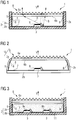
- lighting device 1 has a chip housing 2, in which a radiation emitting semiconductor chip 3 is arranged.
- a chip remote angle filter element 6 is integrated, which is arranged downstream of the radiation-emitting semiconductor chip 3 in a preferred direction V.
- the preferred direction V indicates the direction in which a majority of the radiation emitted by the lighting device 1 is emitted.
- the radiation-emitting semiconductor chip 3 is arranged in a recess 5 of the chip housing 2.
- the recess 5 is bounded by an inner surface 4, which comprises a bottom surface 7 and a plurality of side surfaces 8.
- the side surfaces 8 and the bottom surface 7 are flat, with the side surfaces 8 perpendicular to the bottom surface 7. Since the length of the chip housing 2 is substantially greater than the height, the chip housing 2 has a planar shape.
- the chip package 2 includes a bottom plate 2b having the bottom surface 7 and side walls 2a having the side surfaces 8.
- the bottom plate 2b may include, for example, a ceramic material, particularly a material having high thermal conductivity to sufficiently cool the radiation emitting semiconductor chip 3 during operation. Further, a plastic material is suitable for the side walls 2a.
- the inside of the chip housing 2 may be mirrored, so that the inner surface 4 is reflective.
- the reflectivity of the reflective inner surface 4 is 90% or more, preferably 95% or more, more preferably 98% or more.
- the inner surface 4 is at least ten times as large as the chip surface 9.
- the inner surface 4 is a hundred times larger than the chip surface 9.
- the inner surface 4 1 cm 2 and the chip surface 9 1mm 2 be large.
- the angular filter element 6 has a plurality of pyramid-shaped structural elements 6a with inclined side surfaces.
- the angle between the inclined side surfaces is the same for all structural elements 6a.
- angles are preferred which are between 70 ° and 110 °. It is also conceivable that different angles between the inclined side surfaces are used.
- contours of the structural elements 6a can be suppressed on an illuminated surface.
- pattern formation can be prevented by rotating non-rotationally symmetrical structural elements 6a against one another and / or having different shapes and / or irregularly arranged.
- the structural elements 6a are arranged on a surface of the angular filter element 6 facing away from the semiconductor chip 3, the structural elements 6a tapering in the preferred direction V.
- a surface 6b of the angle filter element 6 facing the semiconductor chip 3 is planar.
- the surface 6b is located in a main plane of the angle filter element 6.
- the main plane is arranged parallel to a radiation exit plane of the illumination device 1 and perpendicular to the preferred direction V.
- the angle filter element 6 can be, for example, an injection-molded part or can be produced from a carrier plate onto which a lacquer layer is applied, from which the structure elements 6a are formed.
- a portion of the radiation emitted by the semiconductor chip 3 may initially impinge on the angular filter element 6. There, a first radiation component is transmitted through the angular filter element 6, while a second radiation component is reflected back into the chip housing 2.
- the light beams which are at an incident angle which lies within the second incident angle range, ie light beams with a relatively large angle of incidence, are transmitted through the angular filter element 6. This is in the FIG. 1 illustrated by the light beam A.
- the light beam A impinges on the surface 6b of the angular filter element 6 and is "broken down" to the incidence solder, wherein the angle of incidence is greater than the angle of reflection.
- the light beam A passes through the angular filter element 6 and impinges on the inclined side surface of the structural element 6a at an uncritical angle, so that the light beam A can decouple from the angular filter element 6.
- the light beam A is "broken away" by the incidence solder and as a result deflected in the preferred direction V.
- Lich rays having an incident angle which is within the first incident angle range that is, light rays having a relatively small angle of incidence, can be reflected by the angular filter element 6 in the present embodiment. This is in the FIG. 1 illustrated by the light beam B.
- the light beam B strikes the surface 6b of the angular filter element 6 essentially parallel to the preferred direction V and is therefore hardly deflected.
- the light beam B is totally reflected and impinges on the opposite side surface of the structural element 6a.
- the light beam B is again totally reflected.
- the light beam B returns to the chip housing 2 and is reflected there, in particular on the inner surface 4, until the light beam B strikes and decouples at an uncritical angle onto the angular filter element 6.
- the light beam B then has a direction which deviates slightly from the preferred direction V.
- the radiation emitted by the lighting device 1 can advantageously be mixed by means of the angular filter element 6, that is to say that light beams of the first and the second angular range are equally present in any area of a radiation level of the lighting device 1.
- beam shaping of the radiation emitted by the lighting device 1 can be effected by means of the present angular filter element 6.
- the emission angle is restricted by means of the angular filter element 6.
- the radiation-emitting semiconductor chip 3 in the embodiment of the FIG. 1 a nitride compound semiconductor and is a thin film semiconductor chip.
- a semiconductor layer sequence comprising a radiation-emitting active layer is first epitaxially grown on a growth substrate. Then, a carrier is applied to a surface of the semiconductor layer sequence lying opposite the growth substrate and subsequently the growth substrate is separated off.
- the growth substrates used for nitride compound semiconductors such as SiC, sapphire or GaN, are comparatively expensive, this method offers the particular advantage that the growth substrate is recyclable.
- a basic principle of a thin-film LED is, for example, in I. Schnitzer et al., Appl. Phys. Lett. 63 (16), 18 October 1993, 2174-2176 described.
- the thin-film semiconductor chip is a Lambert radiator with advantageous coupling-out efficiency.
- the angle filter element 6 is inserted into the chip housing 2 with an exact fit and covers the recess 5 of the chip housing 2. Thus, the radiation-emitting semiconductor chip 3 before external influences such as moisture, dust or other foreign bodies are protected.
- a cavity formed between the radiation-emitting semiconductor chip 3 and the angular filter element 6 is filled with air in this exemplary embodiment.
- FIG. 2 illustrated lighting device 1 has a similar structure as the lighting device of FIG. 1 on.
- the side walls 2a and the angle filter element 6 integrally formed.
- the self-supporting attachment 10 thus formed is an injection-molded part. The attachment 10 is slipped over the semiconductor chip 3 and arranged on the bottom plate 2b.
- the side walls 2a may be provided with a reflector layer before the cap 10 is placed on the bottom plate 2b, so that, as a result, the side surface 8 is reflective.
- FIG. 3 shows a lighting device 1, which has a plurality of radiation emitting semiconductor chips 3.
- the radiation-emitting semiconductor chips 3 are arranged side by side on the bottom plate 2b.
- the entire chip area is composed of a sum of the individual chip areas 9a and 9b.
- the reflective inner surface 4 is at least ten times as large, preferably one hundred times larger than the sum of the individual chip areas 9a and 9b.
- the radiation-emitting semiconductor chips 3 generate radiation with different wavelengths.
- the lighting device 1 includes at least one semiconductor chip that generates red light, one that generates blue light, and one that generates green light, so that white light is emitted from the lighting device 1 as a whole.
- the differently colored radiation in the radiation exit plane can be advantageously mixed, so that no differently colored spots of light occur.
- the depression 5 is partially filled with a filling compound 11.
- a filling compound 11 As a result, the radiation extraction from the semiconductor chip 3 can be improved. Furthermore, by means of an air gap between the filling compound 11 and the angular filter element 6, an advantageously high Refractive index jump can be achieved at the transition to the angular filter element.
- the in the FIGS. 4A and 4B illustrated lighting device 1 has a chip package 2 with a round outline and a plurality of radiation emitting semiconductor chips 3, which are arranged on inner side surfaces 8 of the chip package 2.
- the chip housing 2 has a plurality of recesses 5, which are arranged along an outer wall 12 of the lighting device 1. An illuminated by such a lighting device 1 surface represents a light ring.
- the semiconductor chips 3 opposite side surfaces 8 are concavely curved. As a result, an advantageous deflection of the radiation generated by the semiconductor chips 3 in the preferred direction V take place.
- the depressions 5 are separated from one another by the chip housing 2, a mixing of the radiation generated by the individual semiconductor chips 3 can nevertheless be achieved in the radiation exit plane by means of the angular filter element 6.
- the extraction efficiency E of a lighting device according to the invention is plotted over the reflectivity R of the reflective inner surface.
- the extraction efficiency E of the Lighting device can be increased.
- a reflectivity R 95%
- 85% of the radiation generated by the semiconductor chip or the semiconductor chips can be coupled out of the illumination device.
- FIG. 6 shows the radiation intensity distribution of a Lambert radiator in the radiation exit plane.
- the black circular line indicates a beam angle of 38 °.
- the Lambert radiator almost completely illuminates the circular area within the black circular line.
- the emission angle can be restricted such that, as in FIG. 7 shown only an inner part of the limited by the black circle circular area is illuminated. In this inner part, a homogeneous distribution of the radiation intensity occurs.
Claims (13)
- Dispositif d'éclairage (1) comportant- un boîtier de puce (2) présentant au moins une cavité (5) délimitée par une surface intérieure réfléchissante (4),- au moins une puce à semi-conductrice émettant un rayonnement (3), présentant une surface de puce (9), logée dans la cavité (5),- un élément de filtrage angulaire (6), éloignée de la puce, qui est intégré dans le boîtier de puce (2) et disposé en aval de la puce à semi- conductrice (3) dans une direction préférentielle (V), la surface intérieure réfléchissante (4) étant au moins dix fois plus grande que la surface de puce (9),où le rayonnement émis par la puce à semi- conductrice (3) atteint l'élément de filtrage angulaire (6) et est reflété plus fortement dans une première plage d'angles d'incidence que dans une deuxième plage d'angles d'incidence, la première plage d'angles d'incidence comprenant des angles d'incidence plus petits que la deuxième plage d'angles d'incidence.
- Dispositif d'éclairage (1) selon la revendication 1, la surface intérieure réfléchissante (4) étant cent fois plus grande que la surface de puce (9).
- Dispositif d'éclairage (1) selon l'une quelconque des revendications précédentes,
la surface intérieure réfléchissante (4) présentant une réflectivité de 90 % ou plus, de préférence de 95 % ou plus, de préférence particulièrement de 98 % ou plus. - Dispositif d'éclairage (1) selon l'une quelconque des revendications précédentes,
l'angle de départ du rayonnement émis par le dispositif d'éclairage (1) étant réduit par l'intermédiaire de l'élément de filtrage angulaire (6). - Dispositif d'éclairage (1) selon l'une quelconque des revendications précédentes,
la surface intérieure réfléchissante (4) comportant au moins une surface latérale (8). - Dispositif d'éclairage (1) selon la revendication 5,
la surface latérale (8) présentant une courbure concave. - Dispositif d'éclairage (1) selon la revendication 6,
la surface intérieure réfléchissante (4) présentant une surface de fond planes (7) et plusieurs surfaces latérales planes (8) qui s'étendent en oblique par rapport à la face de surface de fond (7). - Dispositif d'éclairage (1) selon l'une quelconque des revendications précédentes,
l'élément de filtrage angulaire (6) formant une couverture pour le boîtier de puce (2). - Dispositif d'éclairage (1) selon l'une quelconque des revendications précédentes,
l'élément de filtrage angulaire (6) présentant des éléments de structure (6a) qui sont formés de manière conique, pyramidale, prismatique ou égale à des CPCs inverses. - Dispositif d'éclairage (1) selon la revendication 9,
les éléments de structure (6a) convergeant dans la direction préférentielle (V). - Dispositif d'éclairage (1) selon l'une quelconque des revendications 1 à 8,
l'élément de filtrage angulaire (6) étant un filtre diélectrique. - Dispositif d'éclairage (1) selon l'une quelconque des revendications précédentes,
la cavité (5) étant partiellement rempli d'une masse de remplissage (11). - Dispositif d'éclairage (1) selon la revendication 12,
un entrefer existant entre la masse de remplissage (11) et l'élément de filtrage angulaire (6).
Applications Claiming Priority (2)
| Application Number | Priority Date | Filing Date | Title |
|---|---|---|---|
| DE102007057671A DE102007057671A1 (de) | 2007-11-30 | 2007-11-30 | Beleuchtungsvorrichtung |
| PCT/DE2008/001959 WO2009068007A1 (fr) | 2007-11-30 | 2008-11-26 | Dispositif d'éclairage |
Publications (2)
| Publication Number | Publication Date |
|---|---|
| EP2218115A1 EP2218115A1 (fr) | 2010-08-18 |
| EP2218115B1 true EP2218115B1 (fr) | 2018-10-31 |
Family
ID=40512198
Family Applications (1)
| Application Number | Title | Priority Date | Filing Date |
|---|---|---|---|
| EP08855324.3A Not-in-force EP2218115B1 (fr) | 2007-11-30 | 2008-11-26 | Dispositif d'éclairage |
Country Status (8)
| Country | Link |
|---|---|
| US (1) | US20110006324A1 (fr) |
| EP (1) | EP2218115B1 (fr) |
| JP (1) | JP2011505057A (fr) |
| KR (1) | KR20100099238A (fr) |
| CN (1) | CN101878542B (fr) |
| DE (1) | DE102007057671A1 (fr) |
| TW (1) | TWI398606B (fr) |
| WO (1) | WO2009068007A1 (fr) |
Families Citing this family (8)
| Publication number | Priority date | Publication date | Assignee | Title |
|---|---|---|---|---|
| WO2011033424A1 (fr) * | 2009-09-21 | 2011-03-24 | Koninklijke Philips Electronics N.V. | Dispositif électroluminescent comprenant une plaque guide de lumière dotée d'une protection réfléchissante réduisant l'éblouissement |
| DE102010032041A1 (de) * | 2010-07-23 | 2012-01-26 | Osram Opto Semiconductors Gmbh | Strahlungsemittierendes Bauelement und Verfahren zur Herstellung von strahlungsemittierenden Bauelemnenten |
| DE102010038396B4 (de) | 2010-07-26 | 2021-08-05 | OSRAM Opto Semiconductors Gesellschaft mit beschränkter Haftung | Optoelektronisches Bauelement und Leuchtvorrichung damit |
| JP5674444B2 (ja) * | 2010-12-09 | 2015-02-25 | 株式会社モデュレックス | 照明器具 |
| JP6025367B2 (ja) * | 2011-05-12 | 2016-11-16 | キヤノン株式会社 | 有機el素子 |
| DE102013217709A1 (de) * | 2013-09-05 | 2015-03-05 | Carl Zeiss Microscopy Gmbh | Beleuchtungsvorrichtung und digitaler Profilprojektor |
| DE102016101614A1 (de) | 2016-01-29 | 2017-08-03 | Osram Opto Semiconductors Gmbh | Leuchtvorrichtung |
| CN115025253B (zh) * | 2022-06-02 | 2023-10-20 | 星际光(上海)实业有限公司 | 紫外线灯和紫外线灯的滤片结构 |
Family Cites Families (19)
| Publication number | Priority date | Publication date | Assignee | Title |
|---|---|---|---|---|
| DE19654418A1 (de) * | 1996-12-24 | 1998-06-25 | Mannesmann Vdo Ag | Anzeigeeinheit |
| US6155699A (en) * | 1999-03-15 | 2000-12-05 | Agilent Technologies, Inc. | Efficient phosphor-conversion led structure |
| US6490104B1 (en) * | 2000-09-15 | 2002-12-03 | Three-Five Systems, Inc. | Illumination system for a micro display |
| US6686676B2 (en) * | 2001-04-30 | 2004-02-03 | General Electric Company | UV reflectors and UV-based light sources having reduced UV radiation leakage incorporating the same |
| JP4504662B2 (ja) * | 2003-04-09 | 2010-07-14 | シチズン電子株式会社 | Ledランプ |
| JP2005243973A (ja) * | 2004-02-26 | 2005-09-08 | Kyocera Corp | 発光装置および照明装置 |
| US7553683B2 (en) * | 2004-06-09 | 2009-06-30 | Philips Lumiled Lighting Co., Llc | Method of forming pre-fabricated wavelength converting elements for semiconductor light emitting devices |
| JP2006049657A (ja) * | 2004-08-06 | 2006-02-16 | Citizen Electronics Co Ltd | Ledランプ |
| TWI241038B (en) * | 2004-09-14 | 2005-10-01 | Ind Tech Res Inst | Light emitting diode structure and fabrication method thereof |
| US7631991B2 (en) * | 2004-09-30 | 2009-12-15 | Koninklijke Philips Electronics N.V. | Brightness enhancement of LED using selective ray angular recycling |
| DE102004056252A1 (de) * | 2004-10-29 | 2006-05-04 | Osram Opto Semiconductors Gmbh | Beleuchtungseinrichtung, Kfz-Scheinwerfer und Verfahren zur Herstellung einer Beleuchtungseinrichtung |
| TWI239671B (en) * | 2004-12-30 | 2005-09-11 | Ind Tech Res Inst | LED applied with omnidirectional reflector |
| KR100649641B1 (ko) * | 2005-05-31 | 2006-11-27 | 삼성전기주식회사 | Led 패키지 |
| US20060285332A1 (en) * | 2005-06-15 | 2006-12-21 | Goon Wooi K | Compact LED package with reduced field angle |
| JP4984512B2 (ja) * | 2005-12-09 | 2012-07-25 | ソニー株式会社 | 面発光装置及び液晶表示装置 |
| JP2007256874A (ja) * | 2006-03-27 | 2007-10-04 | Matsushita Electric Ind Co Ltd | 面状偏光光源装置及び液晶表示装置 |
| US20070262714A1 (en) * | 2006-05-15 | 2007-11-15 | X-Rite, Incorporated | Illumination source including photoluminescent material and a filter, and an apparatus including same |
| KR100770424B1 (ko) * | 2006-12-13 | 2007-10-26 | 삼성전기주식회사 | 발광 다이오드 패키지 및 그 제조 방법 |
| US8889517B2 (en) * | 2012-04-02 | 2014-11-18 | Jds Uniphase Corporation | Broadband dielectric reflectors for LED with varying thickness |
-
2007
- 2007-11-30 DE DE102007057671A patent/DE102007057671A1/de not_active Withdrawn
-
2008
- 2008-11-26 KR KR1020107014577A patent/KR20100099238A/ko not_active Application Discontinuation
- 2008-11-26 CN CN2008801183322A patent/CN101878542B/zh not_active Expired - Fee Related
- 2008-11-26 WO PCT/DE2008/001959 patent/WO2009068007A1/fr active Application Filing
- 2008-11-26 US US12/744,465 patent/US20110006324A1/en not_active Abandoned
- 2008-11-26 JP JP2010535213A patent/JP2011505057A/ja active Pending
- 2008-11-26 EP EP08855324.3A patent/EP2218115B1/fr not_active Not-in-force
- 2008-11-28 TW TW097146114A patent/TWI398606B/zh not_active IP Right Cessation
Non-Patent Citations (1)
| Title |
|---|
| None * |
Also Published As
| Publication number | Publication date |
|---|---|
| TWI398606B (zh) | 2013-06-11 |
| DE102007057671A1 (de) | 2009-06-04 |
| KR20100099238A (ko) | 2010-09-10 |
| TW200928224A (en) | 2009-07-01 |
| US20110006324A1 (en) | 2011-01-13 |
| CN101878542A (zh) | 2010-11-03 |
| EP2218115A1 (fr) | 2010-08-18 |
| JP2011505057A (ja) | 2011-02-17 |
| CN101878542B (zh) | 2012-09-26 |
| WO2009068007A1 (fr) | 2009-06-04 |
Similar Documents
| Publication | Publication Date | Title |
|---|---|---|
| EP2218115B1 (fr) | Dispositif d'éclairage | |
| EP1621918B1 (fr) | Dispositif comprenant des diodes lumineuses permettant l'illumination homogène d'une zone rectangulaire et illumination de secours | |
| EP1770793B1 (fr) | Dispositif optoélectronique émettant de rayonnement electromagnetique et procédé pour la fabrication d'un tel dispositif | |
| EP2149163B9 (fr) | Puce de diode électroluminescente avec élément d'angle filtrant | |
| DE102005030128B4 (de) | Lichtemittierende Vorrichtung und Beleuchtungsvorrichtung | |
| DE102005048408B4 (de) | Dünnfilm-Halbleiterkörper | |
| EP2583319B1 (fr) | Composant optoélectronique | |
| EP2067177B1 (fr) | Composant opto-électronique | |
| DE102011102350A1 (de) | Optisches Element, optoelektronisches Bauelement und Verfahren zur Herstellung dieser | |
| WO2006045287A2 (fr) | Dispositif a semiconducteur emettant un rayonnement electromagnetique et boitier dudit dispositif | |
| DE112015004324T5 (de) | Strukturierter Dünnfilm-Wellenlängenkonverter und Verfahren zu dessen Herstellung | |
| DE102011080458A1 (de) | Optoelektronische anordnung und verfahren zur herstellung einer optoelektronischen anordnung | |
| DE102018129068A1 (de) | Lichtemittierende Vorrichtung und Verfahren zur Herstellung derselben | |
| WO2011151156A1 (fr) | Élément de conversion de longueur d'onde, élément de construction optoélectronique doté d'un élément de conversion de longueur d'onde et procédé de fabrication d'un élément de conversion de longueur d'onde | |
| DE102009058006A1 (de) | Optoelektronisches Halbleiterbauteil | |
| DE102011015726A1 (de) | Halbleiterchip, Display mit einer Mehrzahl von Halbleiterchips und Verfahren zu deren Herstellung | |
| WO2021170668A1 (fr) | Composant optoélectronique et son procédé de fabrication | |
| WO2021204653A1 (fr) | Composant semi-conducteur et procédé de production de composant semi-conducteur | |
| DE102016104602A1 (de) | Halbleiterlichtquelle | |
| WO2019234185A1 (fr) | Composant à semi-conducteur optoélectronique | |
| WO2018162420A1 (fr) | Composant à semi-conducteur optoélectronique | |
| DE102019104978B4 (de) | Bauteil mit homogenisierter leuchtfläche | |
| DE102010032302A1 (de) | Optoelektronisches Halbleiterbauteil | |
| DE102016105988A1 (de) | Konverter zur teilweisen Konversion einer Primärstrahlung und lichtemittierendes Bauelement | |
| DE112020005291T5 (de) | Leuchtstoffelement, Leuchtstoffvorrichtung und Beleuchtungseinrichtung |
Legal Events
| Date | Code | Title | Description |
|---|---|---|---|
| PUAI | Public reference made under article 153(3) epc to a published international application that has entered the european phase |
Free format text: ORIGINAL CODE: 0009012 |
|
| 17P | Request for examination filed |
Effective date: 20100503 |
|
| AK | Designated contracting states |
Kind code of ref document: A1 Designated state(s): AT BE BG CH CY CZ DE DK EE ES FI FR GB GR HR HU IE IS IT LI LT LU LV MC MT NL NO PL PT RO SE SI SK TR |
|
| AX | Request for extension of the european patent |
Extension state: AL BA MK RS |
|
| DAX | Request for extension of the european patent (deleted) | ||
| 17Q | First examination report despatched |
Effective date: 20131204 |
|
| REG | Reference to a national code |
Ref country code: DE Ref legal event code: R079 Ref document number: 502008016431 Country of ref document: DE Free format text: PREVIOUS MAIN CLASS: H01L0033000000 Ipc: H01L0033580000 |
|
| RIC1 | Information provided on ipc code assigned before grant |
Ipc: H01L 33/58 20100101AFI20180418BHEP |
|
| GRAP | Despatch of communication of intention to grant a patent |
Free format text: ORIGINAL CODE: EPIDOSNIGR1 |
|
| INTG | Intention to grant announced |
Effective date: 20180528 |
|
| GRAS | Grant fee paid |
Free format text: ORIGINAL CODE: EPIDOSNIGR3 |
|
| GRAA | (expected) grant |
Free format text: ORIGINAL CODE: 0009210 |
|
| AK | Designated contracting states |
Kind code of ref document: B1 Designated state(s): AT BE BG CH CY CZ DE DK EE ES FI FR GB GR HR HU IE IS IT LI LT LU LV MC MT NL NO PL PT RO SE SI SK TR |
|
| REG | Reference to a national code |
Ref country code: CH Ref legal event code: EP Ref country code: GB Ref legal event code: FG4D Free format text: NOT ENGLISH |
|
| REG | Reference to a national code |
Ref country code: AT Ref legal event code: REF Ref document number: 1060442 Country of ref document: AT Kind code of ref document: T Effective date: 20181115 |
|
| REG | Reference to a national code |
Ref country code: DE Ref legal event code: R096 Ref document number: 502008016431 Country of ref document: DE |
|
| REG | Reference to a national code |
Ref country code: IE Ref legal event code: FG4D Free format text: LANGUAGE OF EP DOCUMENT: GERMAN |
|
| PGFP | Annual fee paid to national office [announced via postgrant information from national office to epo] |
Ref country code: DE Payment date: 20181120 Year of fee payment: 11 |
|
| REG | Reference to a national code |
Ref country code: NL Ref legal event code: MP Effective date: 20181031 |
|
| REG | Reference to a national code |
Ref country code: LT Ref legal event code: MG4D |
|
| PG25 | Lapsed in a contracting state [announced via postgrant information from national office to epo] |
Ref country code: FI Free format text: LAPSE BECAUSE OF FAILURE TO SUBMIT A TRANSLATION OF THE DESCRIPTION OR TO PAY THE FEE WITHIN THE PRESCRIBED TIME-LIMIT Effective date: 20181031 Ref country code: BG Free format text: LAPSE BECAUSE OF FAILURE TO SUBMIT A TRANSLATION OF THE DESCRIPTION OR TO PAY THE FEE WITHIN THE PRESCRIBED TIME-LIMIT Effective date: 20190131 Ref country code: LT Free format text: LAPSE BECAUSE OF FAILURE TO SUBMIT A TRANSLATION OF THE DESCRIPTION OR TO PAY THE FEE WITHIN THE PRESCRIBED TIME-LIMIT Effective date: 20181031 Ref country code: NO Free format text: LAPSE BECAUSE OF FAILURE TO SUBMIT A TRANSLATION OF THE DESCRIPTION OR TO PAY THE FEE WITHIN THE PRESCRIBED TIME-LIMIT Effective date: 20190131 Ref country code: ES Free format text: LAPSE BECAUSE OF FAILURE TO SUBMIT A TRANSLATION OF THE DESCRIPTION OR TO PAY THE FEE WITHIN THE PRESCRIBED TIME-LIMIT Effective date: 20181031 Ref country code: IS Free format text: LAPSE BECAUSE OF FAILURE TO SUBMIT A TRANSLATION OF THE DESCRIPTION OR TO PAY THE FEE WITHIN THE PRESCRIBED TIME-LIMIT Effective date: 20190228 Ref country code: PL Free format text: LAPSE BECAUSE OF FAILURE TO SUBMIT A TRANSLATION OF THE DESCRIPTION OR TO PAY THE FEE WITHIN THE PRESCRIBED TIME-LIMIT Effective date: 20181031 Ref country code: HR Free format text: LAPSE BECAUSE OF FAILURE TO SUBMIT A TRANSLATION OF THE DESCRIPTION OR TO PAY THE FEE WITHIN THE PRESCRIBED TIME-LIMIT Effective date: 20181031 Ref country code: LV Free format text: LAPSE BECAUSE OF FAILURE TO SUBMIT A TRANSLATION OF THE DESCRIPTION OR TO PAY THE FEE WITHIN THE PRESCRIBED TIME-LIMIT Effective date: 20181031 |
|
| PG25 | Lapsed in a contracting state [announced via postgrant information from national office to epo] |
Ref country code: SE Free format text: LAPSE BECAUSE OF FAILURE TO SUBMIT A TRANSLATION OF THE DESCRIPTION OR TO PAY THE FEE WITHIN THE PRESCRIBED TIME-LIMIT Effective date: 20181031 Ref country code: GR Free format text: LAPSE BECAUSE OF FAILURE TO SUBMIT A TRANSLATION OF THE DESCRIPTION OR TO PAY THE FEE WITHIN THE PRESCRIBED TIME-LIMIT Effective date: 20190201 Ref country code: NL Free format text: LAPSE BECAUSE OF FAILURE TO SUBMIT A TRANSLATION OF THE DESCRIPTION OR TO PAY THE FEE WITHIN THE PRESCRIBED TIME-LIMIT Effective date: 20181031 Ref country code: PT Free format text: LAPSE BECAUSE OF FAILURE TO SUBMIT A TRANSLATION OF THE DESCRIPTION OR TO PAY THE FEE WITHIN THE PRESCRIBED TIME-LIMIT Effective date: 20190301 |
|
| REG | Reference to a national code |
Ref country code: CH Ref legal event code: PL |
|
| PG25 | Lapsed in a contracting state [announced via postgrant information from national office to epo] |
Ref country code: IT Free format text: LAPSE BECAUSE OF FAILURE TO SUBMIT A TRANSLATION OF THE DESCRIPTION OR TO PAY THE FEE WITHIN THE PRESCRIBED TIME-LIMIT Effective date: 20181031 Ref country code: LU Free format text: LAPSE BECAUSE OF NON-PAYMENT OF DUE FEES Effective date: 20181126 Ref country code: DK Free format text: LAPSE BECAUSE OF FAILURE TO SUBMIT A TRANSLATION OF THE DESCRIPTION OR TO PAY THE FEE WITHIN THE PRESCRIBED TIME-LIMIT Effective date: 20181031 Ref country code: CZ Free format text: LAPSE BECAUSE OF FAILURE TO SUBMIT A TRANSLATION OF THE DESCRIPTION OR TO PAY THE FEE WITHIN THE PRESCRIBED TIME-LIMIT Effective date: 20181031 |
|
| REG | Reference to a national code |
Ref country code: DE Ref legal event code: R097 Ref document number: 502008016431 Country of ref document: DE |
|
| REG | Reference to a national code |
Ref country code: BE Ref legal event code: MM Effective date: 20181130 |
|
| REG | Reference to a national code |
Ref country code: IE Ref legal event code: MM4A |
|
| PG25 | Lapsed in a contracting state [announced via postgrant information from national office to epo] |
Ref country code: LI Free format text: LAPSE BECAUSE OF NON-PAYMENT OF DUE FEES Effective date: 20181130 Ref country code: EE Free format text: LAPSE BECAUSE OF FAILURE TO SUBMIT A TRANSLATION OF THE DESCRIPTION OR TO PAY THE FEE WITHIN THE PRESCRIBED TIME-LIMIT Effective date: 20181031 Ref country code: RO Free format text: LAPSE BECAUSE OF FAILURE TO SUBMIT A TRANSLATION OF THE DESCRIPTION OR TO PAY THE FEE WITHIN THE PRESCRIBED TIME-LIMIT Effective date: 20181031 Ref country code: CH Free format text: LAPSE BECAUSE OF NON-PAYMENT OF DUE FEES Effective date: 20181130 Ref country code: MC Free format text: LAPSE BECAUSE OF FAILURE TO SUBMIT A TRANSLATION OF THE DESCRIPTION OR TO PAY THE FEE WITHIN THE PRESCRIBED TIME-LIMIT Effective date: 20181031 Ref country code: SK Free format text: LAPSE BECAUSE OF FAILURE TO SUBMIT A TRANSLATION OF THE DESCRIPTION OR TO PAY THE FEE WITHIN THE PRESCRIBED TIME-LIMIT Effective date: 20181031 |
|
| PLBE | No opposition filed within time limit |
Free format text: ORIGINAL CODE: 0009261 |
|
| STAA | Information on the status of an ep patent application or granted ep patent |
Free format text: STATUS: NO OPPOSITION FILED WITHIN TIME LIMIT |
|
| RAP2 | Party data changed (patent owner data changed or rights of a patent transferred) |
Owner name: OSRAM OPTO SEMICONDUCTORS GMBH |
|
| GBPC | Gb: european patent ceased through non-payment of renewal fee |
Effective date: 20190131 |
|
| 26N | No opposition filed |
Effective date: 20190801 |
|
| PG25 | Lapsed in a contracting state [announced via postgrant information from national office to epo] |
Ref country code: IE Free format text: LAPSE BECAUSE OF NON-PAYMENT OF DUE FEES Effective date: 20181126 Ref country code: SI Free format text: LAPSE BECAUSE OF FAILURE TO SUBMIT A TRANSLATION OF THE DESCRIPTION OR TO PAY THE FEE WITHIN THE PRESCRIBED TIME-LIMIT Effective date: 20181031 Ref country code: FR Free format text: LAPSE BECAUSE OF NON-PAYMENT OF DUE FEES Effective date: 20181231 |
|
| PG25 | Lapsed in a contracting state [announced via postgrant information from national office to epo] |
Ref country code: BE Free format text: LAPSE BECAUSE OF NON-PAYMENT OF DUE FEES Effective date: 20181130 |
|
| PG25 | Lapsed in a contracting state [announced via postgrant information from national office to epo] |
Ref country code: GB Free format text: LAPSE BECAUSE OF NON-PAYMENT OF DUE FEES Effective date: 20190131 |
|
| REG | Reference to a national code |
Ref country code: AT Ref legal event code: MM01 Ref document number: 1060442 Country of ref document: AT Kind code of ref document: T Effective date: 20181126 |
|
| PG25 | Lapsed in a contracting state [announced via postgrant information from national office to epo] |
Ref country code: AT Free format text: LAPSE BECAUSE OF NON-PAYMENT OF DUE FEES Effective date: 20181126 Ref country code: MT Free format text: LAPSE BECAUSE OF FAILURE TO SUBMIT A TRANSLATION OF THE DESCRIPTION OR TO PAY THE FEE WITHIN THE PRESCRIBED TIME-LIMIT Effective date: 20181031 |
|
| PG25 | Lapsed in a contracting state [announced via postgrant information from national office to epo] |
Ref country code: TR Free format text: LAPSE BECAUSE OF FAILURE TO SUBMIT A TRANSLATION OF THE DESCRIPTION OR TO PAY THE FEE WITHIN THE PRESCRIBED TIME-LIMIT Effective date: 20181031 |
|
| REG | Reference to a national code |
Ref country code: DE Ref legal event code: R119 Ref document number: 502008016431 Country of ref document: DE |
|
| PG25 | Lapsed in a contracting state [announced via postgrant information from national office to epo] |
Ref country code: HU Free format text: LAPSE BECAUSE OF FAILURE TO SUBMIT A TRANSLATION OF THE DESCRIPTION OR TO PAY THE FEE WITHIN THE PRESCRIBED TIME-LIMIT; INVALID AB INITIO Effective date: 20081126 Ref country code: CY Free format text: LAPSE BECAUSE OF FAILURE TO SUBMIT A TRANSLATION OF THE DESCRIPTION OR TO PAY THE FEE WITHIN THE PRESCRIBED TIME-LIMIT Effective date: 20181031 |
|
| PG25 | Lapsed in a contracting state [announced via postgrant information from national office to epo] |
Ref country code: DE Free format text: LAPSE BECAUSE OF NON-PAYMENT OF DUE FEES Effective date: 20200603 |