EP2216819A2 - Solid-state image pick-up device and manufacturing method thereof, image-pickup apparatus, semiconductor device and manufacturing method thereof, and semiconductor substrate - Google Patents
Solid-state image pick-up device and manufacturing method thereof, image-pickup apparatus, semiconductor device and manufacturing method thereof, and semiconductor substrate Download PDFInfo
- Publication number
- EP2216819A2 EP2216819A2 EP10152062A EP10152062A EP2216819A2 EP 2216819 A2 EP2216819 A2 EP 2216819A2 EP 10152062 A EP10152062 A EP 10152062A EP 10152062 A EP10152062 A EP 10152062A EP 2216819 A2 EP2216819 A2 EP 2216819A2
- Authority
- EP
- European Patent Office
- Prior art keywords
- layer
- forming
- gettering
- element forming
- conductive type
- Prior art date
- Legal status (The legal status is an assumption and is not a legal conclusion. Google has not performed a legal analysis and makes no representation as to the accuracy of the status listed.)
- Ceased
Links
- 239000004065 semiconductor Substances 0.000 title claims abstract description 333
- 239000000758 substrate Substances 0.000 title claims abstract description 268
- 238000004519 manufacturing process Methods 0.000 title claims description 120
- 238000005247 gettering Methods 0.000 claims abstract description 354
- 238000006243 chemical reaction Methods 0.000 claims abstract description 48
- 238000000034 method Methods 0.000 claims description 130
- 239000012535 impurity Substances 0.000 claims description 88
- 238000005530 etching Methods 0.000 claims description 52
- 238000012545 processing Methods 0.000 claims description 17
- 230000006870 function Effects 0.000 claims description 13
- 238000010438 heat treatment Methods 0.000 claims description 13
- 230000003287 optical effect Effects 0.000 claims description 5
- RTAQQCXQSZGOHL-UHFFFAOYSA-N Titanium Chemical compound [Ti] RTAQQCXQSZGOHL-UHFFFAOYSA-N 0.000 claims description 2
- QCWXUUIWCKQGHC-UHFFFAOYSA-N Zirconium Chemical compound [Zr] QCWXUUIWCKQGHC-UHFFFAOYSA-N 0.000 claims description 2
- 229910052782 aluminium Inorganic materials 0.000 claims description 2
- XAGFODPZIPBFFR-UHFFFAOYSA-N aluminium Chemical compound [Al] XAGFODPZIPBFFR-UHFFFAOYSA-N 0.000 claims description 2
- 229910052747 lanthanoid Inorganic materials 0.000 claims description 2
- 150000002602 lanthanoids Chemical class 0.000 claims description 2
- 229910052715 tantalum Inorganic materials 0.000 claims description 2
- GUVRBAGPIYLISA-UHFFFAOYSA-N tantalum atom Chemical compound [Ta] GUVRBAGPIYLISA-UHFFFAOYSA-N 0.000 claims description 2
- 229910052719 titanium Inorganic materials 0.000 claims description 2
- 239000010936 titanium Substances 0.000 claims description 2
- 229910052727 yttrium Inorganic materials 0.000 claims description 2
- VWQVUPCCIRVNHF-UHFFFAOYSA-N yttrium atom Chemical compound [Y] VWQVUPCCIRVNHF-UHFFFAOYSA-N 0.000 claims description 2
- 229910052726 zirconium Inorganic materials 0.000 claims description 2
- 229910052735 hafnium Inorganic materials 0.000 claims 1
- VBJZVLUMGGDVMO-UHFFFAOYSA-N hafnium atom Chemical compound [Hf] VBJZVLUMGGDVMO-UHFFFAOYSA-N 0.000 claims 1
- 238000003475 lamination Methods 0.000 claims 1
- 238000009825 accumulation Methods 0.000 description 54
- 150000002500 ions Chemical class 0.000 description 43
- 229910000449 hafnium oxide Inorganic materials 0.000 description 42
- WIHZLLGSGQNAGK-UHFFFAOYSA-N hafnium(4+);oxygen(2-) Chemical compound [O-2].[O-2].[Hf+4] WIHZLLGSGQNAGK-UHFFFAOYSA-N 0.000 description 42
- VYPSYNLAJGMNEJ-UHFFFAOYSA-N Silicium dioxide Chemical compound O=[Si]=O VYPSYNLAJGMNEJ-UHFFFAOYSA-N 0.000 description 34
- 238000009792 diffusion process Methods 0.000 description 33
- XUIMIQQOPSSXEZ-UHFFFAOYSA-N Silicon Chemical compound [Si] XUIMIQQOPSSXEZ-UHFFFAOYSA-N 0.000 description 26
- 229910052710 silicon Inorganic materials 0.000 description 26
- 239000010703 silicon Substances 0.000 description 26
- 238000001039 wet etching Methods 0.000 description 25
- 238000012546 transfer Methods 0.000 description 22
- 230000007547 defect Effects 0.000 description 20
- OAICVXFJPJFONN-UHFFFAOYSA-N Phosphorus Chemical compound [P] OAICVXFJPJFONN-UHFFFAOYSA-N 0.000 description 18
- 229910052698 phosphorus Inorganic materials 0.000 description 18
- 239000011574 phosphorus Substances 0.000 description 18
- ZOXJGFHDIHLPTG-UHFFFAOYSA-N Boron Chemical compound [B] ZOXJGFHDIHLPTG-UHFFFAOYSA-N 0.000 description 16
- 229910052796 boron Inorganic materials 0.000 description 16
- 230000000875 corresponding effect Effects 0.000 description 16
- 229910052751 metal Inorganic materials 0.000 description 14
- 239000002184 metal Substances 0.000 description 14
- 238000000137 annealing Methods 0.000 description 12
- 238000011109 contamination Methods 0.000 description 12
- 235000012239 silicon dioxide Nutrition 0.000 description 12
- 239000000377 silicon dioxide Substances 0.000 description 12
- 238000002161 passivation Methods 0.000 description 10
- 229910052814 silicon oxide Inorganic materials 0.000 description 10
- 230000003247 decreasing effect Effects 0.000 description 8
- 238000009413 insulation Methods 0.000 description 8
- 238000007789 sealing Methods 0.000 description 8
- 238000013461 design Methods 0.000 description 7
- 229910001385 heavy metal Inorganic materials 0.000 description 7
- 238000002955 isolation Methods 0.000 description 7
- 230000002411 adverse Effects 0.000 description 5
- 230000015572 biosynthetic process Effects 0.000 description 5
- 238000000231 atomic layer deposition Methods 0.000 description 4
- 229910052799 carbon Inorganic materials 0.000 description 4
- -1 carbon ions Chemical class 0.000 description 4
- 238000005229 chemical vapour deposition Methods 0.000 description 4
- 230000000694 effects Effects 0.000 description 4
- 238000009429 electrical wiring Methods 0.000 description 4
- 238000005468 ion implantation Methods 0.000 description 4
- 230000002093 peripheral effect Effects 0.000 description 4
- 238000005498 polishing Methods 0.000 description 4
- 230000002950 deficient Effects 0.000 description 3
- 150000002739 metals Chemical class 0.000 description 3
- 230000015556 catabolic process Effects 0.000 description 2
- 238000006731 degradation reaction Methods 0.000 description 2
- 239000011159 matrix material Substances 0.000 description 2
- 238000005070 sampling Methods 0.000 description 2
- 230000004075 alteration Effects 0.000 description 1
- 230000002596 correlated effect Effects 0.000 description 1
- 239000013078 crystal Substances 0.000 description 1
- BHEPBYXIRTUNPN-UHFFFAOYSA-N hydridophosphorus(.) (triplet) Chemical compound [PH] BHEPBYXIRTUNPN-UHFFFAOYSA-N 0.000 description 1
- 239000000463 material Substances 0.000 description 1
- 238000012986 modification Methods 0.000 description 1
- 230000004048 modification Effects 0.000 description 1
- 230000003595 spectral effect Effects 0.000 description 1
Images


Classifications
-
- G—PHYSICS
- G01—MEASURING; TESTING
- G01N—INVESTIGATING OR ANALYSING MATERIALS BY DETERMINING THEIR CHEMICAL OR PHYSICAL PROPERTIES
- G01N33/00—Investigating or analysing materials by specific methods not covered by groups G01N1/00 - G01N31/00
- G01N33/48—Biological material, e.g. blood, urine; Haemocytometers
- G01N33/483—Physical analysis of biological material
- G01N33/487—Physical analysis of biological material of liquid biological material
- G01N33/49—Blood
-
- H—ELECTRICITY
- H01—ELECTRIC ELEMENTS
- H01L—SEMICONDUCTOR DEVICES NOT COVERED BY CLASS H10
- H01L27/00—Devices consisting of a plurality of semiconductor or other solid-state components formed in or on a common substrate
- H01L27/14—Devices consisting of a plurality of semiconductor or other solid-state components formed in or on a common substrate including semiconductor components sensitive to infrared radiation, light, electromagnetic radiation of shorter wavelength or corpuscular radiation and specially adapted either for the conversion of the energy of such radiation into electrical energy or for the control of electrical energy by such radiation
- H01L27/144—Devices controlled by radiation
- H01L27/146—Imager structures
- H01L27/14683—Processes or apparatus peculiar to the manufacture or treatment of these devices or parts thereof
- H01L27/14698—Post-treatment for the devices, e.g. annealing, impurity-gettering, shor-circuit elimination, recrystallisation
-
- A—HUMAN NECESSITIES
- A61—MEDICAL OR VETERINARY SCIENCE; HYGIENE
- A61B—DIAGNOSIS; SURGERY; IDENTIFICATION
- A61B5/00—Measuring for diagnostic purposes; Identification of persons
- A61B5/145—Measuring characteristics of blood in vivo, e.g. gas concentration, pH value; Measuring characteristics of body fluids or tissues, e.g. interstitial fluid, cerebral tissue
- A61B5/14546—Measuring characteristics of blood in vivo, e.g. gas concentration, pH value; Measuring characteristics of body fluids or tissues, e.g. interstitial fluid, cerebral tissue for measuring analytes not otherwise provided for, e.g. ions, cytochromes
-
- G—PHYSICS
- G01—MEASURING; TESTING
- G01N—INVESTIGATING OR ANALYSING MATERIALS BY DETERMINING THEIR CHEMICAL OR PHYSICAL PROPERTIES
- G01N9/00—Investigating density or specific gravity of materials; Analysing materials by determining density or specific gravity
- G01N9/36—Analysing materials by measuring the density or specific gravity, e.g. determining quantity of moisture
-
- H—ELECTRICITY
- H01—ELECTRIC ELEMENTS
- H01L—SEMICONDUCTOR DEVICES NOT COVERED BY CLASS H10
- H01L21/00—Processes or apparatus adapted for the manufacture or treatment of semiconductor or solid state devices or of parts thereof
- H01L21/02—Manufacture or treatment of semiconductor devices or of parts thereof
- H01L21/04—Manufacture or treatment of semiconductor devices or of parts thereof the devices having at least one potential-jump barrier or surface barrier, e.g. PN junction, depletion layer or carrier concentration layer
- H01L21/18—Manufacture or treatment of semiconductor devices or of parts thereof the devices having at least one potential-jump barrier or surface barrier, e.g. PN junction, depletion layer or carrier concentration layer the devices having semiconductor bodies comprising elements of Group IV of the Periodic System or AIIIBV compounds with or without impurities, e.g. doping materials
- H01L21/30—Treatment of semiconductor bodies using processes or apparatus not provided for in groups H01L21/20 - H01L21/26
- H01L21/322—Treatment of semiconductor bodies using processes or apparatus not provided for in groups H01L21/20 - H01L21/26 to modify their internal properties, e.g. to produce internal imperfections
- H01L21/3221—Treatment of semiconductor bodies using processes or apparatus not provided for in groups H01L21/20 - H01L21/26 to modify their internal properties, e.g. to produce internal imperfections of silicon bodies, e.g. for gettering
-
- H—ELECTRICITY
- H01—ELECTRIC ELEMENTS
- H01L—SEMICONDUCTOR DEVICES NOT COVERED BY CLASS H10
- H01L27/00—Devices consisting of a plurality of semiconductor or other solid-state components formed in or on a common substrate
- H01L27/14—Devices consisting of a plurality of semiconductor or other solid-state components formed in or on a common substrate including semiconductor components sensitive to infrared radiation, light, electromagnetic radiation of shorter wavelength or corpuscular radiation and specially adapted either for the conversion of the energy of such radiation into electrical energy or for the control of electrical energy by such radiation
- H01L27/144—Devices controlled by radiation
- H01L27/146—Imager structures
- H01L27/14601—Structural or functional details thereof
- H01L27/1464—Back illuminated imager structures
-
- H—ELECTRICITY
- H01—ELECTRIC ELEMENTS
- H01L—SEMICONDUCTOR DEVICES NOT COVERED BY CLASS H10
- H01L27/00—Devices consisting of a plurality of semiconductor or other solid-state components formed in or on a common substrate
- H01L27/14—Devices consisting of a plurality of semiconductor or other solid-state components formed in or on a common substrate including semiconductor components sensitive to infrared radiation, light, electromagnetic radiation of shorter wavelength or corpuscular radiation and specially adapted either for the conversion of the energy of such radiation into electrical energy or for the control of electrical energy by such radiation
- H01L27/144—Devices controlled by radiation
- H01L27/146—Imager structures
- H01L27/14683—Processes or apparatus peculiar to the manufacture or treatment of these devices or parts thereof
- H01L27/14689—MOS based technologies
-
- H—ELECTRICITY
- H01—ELECTRIC ELEMENTS
- H01L—SEMICONDUCTOR DEVICES NOT COVERED BY CLASS H10
- H01L31/00—Semiconductor devices sensitive to infrared radiation, light, electromagnetic radiation of shorter wavelength or corpuscular radiation and specially adapted either for the conversion of the energy of such radiation into electrical energy or for the control of electrical energy by such radiation; Processes or apparatus specially adapted for the manufacture or treatment thereof or of parts thereof; Details thereof
- H01L31/18—Processes or apparatus specially adapted for the manufacture or treatment of these devices or of parts thereof
-
- H—ELECTRICITY
- H01—ELECTRIC ELEMENTS
- H01L—SEMICONDUCTOR DEVICES NOT COVERED BY CLASS H10
- H01L21/00—Processes or apparatus adapted for the manufacture or treatment of semiconductor or solid state devices or of parts thereof
- H01L21/70—Manufacture or treatment of devices consisting of a plurality of solid state components formed in or on a common substrate or of parts thereof; Manufacture of integrated circuit devices or of parts thereof
- H01L21/71—Manufacture of specific parts of devices defined in group H01L21/70
- H01L21/76—Making of isolation regions between components
- H01L21/762—Dielectric regions, e.g. EPIC dielectric isolation, LOCOS; Trench refilling techniques, SOI technology, use of channel stoppers
- H01L21/7624—Dielectric regions, e.g. EPIC dielectric isolation, LOCOS; Trench refilling techniques, SOI technology, use of channel stoppers using semiconductor on insulator [SOI] technology
- H01L21/76251—Dielectric regions, e.g. EPIC dielectric isolation, LOCOS; Trench refilling techniques, SOI technology, use of channel stoppers using semiconductor on insulator [SOI] technology using bonding techniques
- H01L21/76256—Dielectric regions, e.g. EPIC dielectric isolation, LOCOS; Trench refilling techniques, SOI technology, use of channel stoppers using semiconductor on insulator [SOI] technology using bonding techniques using silicon etch back techniques, e.g. BESOI, ELTRAN
-
- H—ELECTRICITY
- H01—ELECTRIC ELEMENTS
- H01L—SEMICONDUCTOR DEVICES NOT COVERED BY CLASS H10
- H01L27/00—Devices consisting of a plurality of semiconductor or other solid-state components formed in or on a common substrate
- H01L27/02—Devices consisting of a plurality of semiconductor or other solid-state components formed in or on a common substrate including semiconductor components specially adapted for rectifying, oscillating, amplifying or switching and having at least one potential-jump barrier or surface barrier; including integrated passive circuit elements with at least one potential-jump barrier or surface barrier
- H01L27/12—Devices consisting of a plurality of semiconductor or other solid-state components formed in or on a common substrate including semiconductor components specially adapted for rectifying, oscillating, amplifying or switching and having at least one potential-jump barrier or surface barrier; including integrated passive circuit elements with at least one potential-jump barrier or surface barrier the substrate being other than a semiconductor body, e.g. an insulating body
- H01L27/1203—Devices consisting of a plurality of semiconductor or other solid-state components formed in or on a common substrate including semiconductor components specially adapted for rectifying, oscillating, amplifying or switching and having at least one potential-jump barrier or surface barrier; including integrated passive circuit elements with at least one potential-jump barrier or surface barrier the substrate being other than a semiconductor body, e.g. an insulating body the substrate comprising an insulating body on a semiconductor body, e.g. SOI
-
- H—ELECTRICITY
- H01—ELECTRIC ELEMENTS
- H01L—SEMICONDUCTOR DEVICES NOT COVERED BY CLASS H10
- H01L27/00—Devices consisting of a plurality of semiconductor or other solid-state components formed in or on a common substrate
- H01L27/14—Devices consisting of a plurality of semiconductor or other solid-state components formed in or on a common substrate including semiconductor components sensitive to infrared radiation, light, electromagnetic radiation of shorter wavelength or corpuscular radiation and specially adapted either for the conversion of the energy of such radiation into electrical energy or for the control of electrical energy by such radiation
- H01L27/144—Devices controlled by radiation
- H01L27/146—Imager structures
- H01L27/14601—Structural or functional details thereof
- H01L27/14609—Pixel-elements with integrated switching, control, storage or amplification elements
-
- H—ELECTRICITY
- H01—ELECTRIC ELEMENTS
- H01L—SEMICONDUCTOR DEVICES NOT COVERED BY CLASS H10
- H01L27/00—Devices consisting of a plurality of semiconductor or other solid-state components formed in or on a common substrate
- H01L27/14—Devices consisting of a plurality of semiconductor or other solid-state components formed in or on a common substrate including semiconductor components sensitive to infrared radiation, light, electromagnetic radiation of shorter wavelength or corpuscular radiation and specially adapted either for the conversion of the energy of such radiation into electrical energy or for the control of electrical energy by such radiation
- H01L27/144—Devices controlled by radiation
- H01L27/146—Imager structures
- H01L27/14601—Structural or functional details thereof
- H01L27/14632—Wafer-level processed structures
-
- H—ELECTRICITY
- H01—ELECTRIC ELEMENTS
- H01L—SEMICONDUCTOR DEVICES NOT COVERED BY CLASS H10
- H01L27/00—Devices consisting of a plurality of semiconductor or other solid-state components formed in or on a common substrate
- H01L27/14—Devices consisting of a plurality of semiconductor or other solid-state components formed in or on a common substrate including semiconductor components sensitive to infrared radiation, light, electromagnetic radiation of shorter wavelength or corpuscular radiation and specially adapted either for the conversion of the energy of such radiation into electrical energy or for the control of electrical energy by such radiation
- H01L27/144—Devices controlled by radiation
- H01L27/146—Imager structures
- H01L27/14601—Structural or functional details thereof
- H01L27/14636—Interconnect structures
-
- H—ELECTRICITY
- H01—ELECTRIC ELEMENTS
- H01L—SEMICONDUCTOR DEVICES NOT COVERED BY CLASS H10
- H01L27/00—Devices consisting of a plurality of semiconductor or other solid-state components formed in or on a common substrate
- H01L27/14—Devices consisting of a plurality of semiconductor or other solid-state components formed in or on a common substrate including semiconductor components sensitive to infrared radiation, light, electromagnetic radiation of shorter wavelength or corpuscular radiation and specially adapted either for the conversion of the energy of such radiation into electrical energy or for the control of electrical energy by such radiation
- H01L27/144—Devices controlled by radiation
- H01L27/146—Imager structures
- H01L27/14643—Photodiode arrays; MOS imagers
-
- H—ELECTRICITY
- H01—ELECTRIC ELEMENTS
- H01L—SEMICONDUCTOR DEVICES NOT COVERED BY CLASS H10
- H01L27/00—Devices consisting of a plurality of semiconductor or other solid-state components formed in or on a common substrate
- H01L27/14—Devices consisting of a plurality of semiconductor or other solid-state components formed in or on a common substrate including semiconductor components sensitive to infrared radiation, light, electromagnetic radiation of shorter wavelength or corpuscular radiation and specially adapted either for the conversion of the energy of such radiation into electrical energy or for the control of electrical energy by such radiation
- H01L27/144—Devices controlled by radiation
- H01L27/146—Imager structures
- H01L27/14683—Processes or apparatus peculiar to the manufacture or treatment of these devices or parts thereof
- H01L27/14685—Process for coatings or optical elements
Definitions
- the present invention relates to a solid-state image pick-up device and a manufacturing method thereof; an image pick-up apparatus; a semiconductor device and a manufacturing method thereof; and a semiconductor substrate.
- the present invention relates to a solid-state image pick-up device in which a gettering layer is provided on an upper layer of an element forming layer to suppress metal contamination and a manufacturing method of the solid-state image pick-up device; an image pick-up apparatus; a semiconductor device and a manufacturing method thereof; and a semiconductor substrate.
- a thin semiconductor device having a high strength such as a rear surface irradiation type solid-state image pick-up device, has an element forming layer and a wiring layer provided on one surface of the element forming layer.
- the element forming layer photoelectric conversion elements and active elements are formed, and the active elements convert signal charges which are photoelectric-converted by the photoelectric conversion elements into electrical signals and output the electrical signals.
- the wiring layer performs wiring of the active elements formed in the element forming layer. Furthermore, it is configured such that visible light is incident on the photoelectric conversion elements from one surface of the element forming layer located at a side opposite to that of the wiring layer (see for example, Japanese Unexamined Patent Application Publication No. 2003-31785 ).
- the element forming layer is preferably formed to have a desired small thickness.
- the thickness thereof is preferably decreased to 10 ⁇ m or less.
- a silicon substrate having an SOI structure is used in which an element forming layer (SOI layer) made of silicon is formed on a silicon substrate functioning as a support substrate with a SiO 2 film (BOX layer) interposed therebetween.
- SOI layer element forming layer
- BOX layer SiO 2 film
- a rear surface irradiation type solid-state image pick-up device is formed using a semiconductor substrate which has an SOI structure.
- a silicon oxide film (SiO 2 ) 102 having a thickness of approximately 1 ⁇ m is formed on a surface of a silicon substrate 101 functioning as a support substrate, and an element forming layer 103 having an SOI structure is formed on the silicon oxide film 102.
- the element forming layer 103 there are formed photoelectric conversion elements 104 and active elements (not shown) which convert signal charges photoelectric-converted by the photoelectric conversion elements into electrical signals and which output the above signals.
- a wiring layer 105 which performs wiring of the active elements is formed on the surface of the element forming layer 103.
- the thickness of the semiconductor substrate is decreased from a rear surface side (visible light incident side), so that only the element forming layer 103 is allowed to remain.
- the silicon oxide film 102 is formed in the semiconductor substrate. Hence, when the thickness of the semiconductor substrate is decreased by wet etching, the etching can be stopped by the silicon oxide film 102. In addition, when the silicon oxide film 102 is subsequently peeled away, only the element forming layer 103 may be allowed to remain.
- a method for manufacturing a semiconductor substrate including a different type of material (SiO 2 ), such as a semiconductor substrate having an SOI structure is complicated, and the product obtained by the method described above is expensive.
- a gettering layer is not formed in the element forming layer 103, after the silicon oxide film 102 is removed, it is difficult to prevent metal contamination caused by heavy metals in various processes.
- the gettering effect described above may not be sufficiently obtained.
- the gettering layer formed in the semiconductor substrate at a rear surface side is also removed, and hence in a process after the gettering layer is removed, no gettering effect can be obtained.
- a gettering layer is formed in a deep region of an SOI layer which is close to a BOX layer.
- the gettering layer is provided in a deep region of the SOI layer, in the case in which elements are formed not only in a surface region of the SOI layer but also in a region thereof in a depth direction, degradation in element characteristics caused by crystalline defects derived from the gettering layer may occur in some cases.
- the gettering layer is a defective layer formed in a silicon single crystal, and even when a silicon substrate is metal-contaminated, the defective layer collects metals using heat generated in a wafer process. Hence, the influence of contamination can be suppressed in a silicon substrate in which elements are formed.
- the gettering layer is formed from a defective layer, electrons and the like generated therefrom as described above may adversely cause noises in some cases. Hence, as described above, it is believed that electrons and the like generated due to the presence of the gettering layer may cause noises.
- the present invention has been conceived in consideration of the problems described above, and it is desirable to provide a solid-state image pick-up device which can suppress noises generated due to the presence of a gettering layer and a manufacturing method of the solid-state image pick-up device; an image pick-up apparatus; a semiconductor device and a manufacturing method thereof; and a semiconductor substrate.
- a solid-state image pick-up device which includes a semiconductor substrate main body which includes an element forming layer and a gettering layer provided on an upper layer thereof; photoelectric conversion elements, each of which includes a first conductive type region, provided in the element forming layer; and a dielectric film which is provided on an upper layer of the gettering layer and which induces a second conductive type region in a surface of the gettering layer.
- an image pick-up apparatus which includes a solid-state image pick-up device including a semiconductor substrate main body which has an element forming layer and a gettering layer provided on an upper layer thereof; photoelectric conversion elements, each of which includes a first conductive type region, formed in the element forming layer; and a dielectric film which is provided on an upper layer of the gettering layer and which induces a second conductive type region in a surface of the gettering layer; an optical system for guiding incident light from an object to the solid-state image pick-up device; and a signal processing circuit for processing an output signal from the solid-state image pick-up device.
- a semiconductor device which includes: a semiconductor substrate main body which includes an element forming layer and a gettering layer provided on an upper layer of the element forming layer; a device which includes a first conductive type region and is formed in the element forming layer; and a dielectric film which is provided on an upper layer of the gettering layer and which induces a second conductive type region in a surface of the gettering layer.
- a semiconductor substrate which includes: a semiconductor substrate main body which includes an element forming layer in which a device including a first conductive type region is provided and a gettering layer provided on an upper layer of the element forming layer; and a dielectric film which is provided on an upper layer of the gettering layer and which induced a second conductive type region in a surface of the gettering layer.
- the second conductive type region is induced in the surface of the gettering layer by the dielectric film, even if electrons are generated due to crystalline defects of the gettering layer, electrons and holes are combined with each other in the surface of the gettering layer, and hence electrons are not likely to enter devices, such as photoelectric conversion elements, provided in the element forming layer.
- a solid-state image pick-up device which includes: an element forming layer in which photoelectric conversion elements each including a first conductive type region are provided; a second conductive type impurity region provided on an upper layer of the element forming layer; and a gettering layer provided on an upper layer of the impurity region.
- an image pick-up apparatus which includes: a solid-state image pick-up device including an element forming layer in which photoelectric conversion elements each including a first conductive type region are formed, a second conductive type impurity region provided on an upper layer of the element forming layer, and a gettering layer provided on an upper layer of the impurity region; an optical system for guiding incident light from an object to the solid-state image pick-up device; and a signal processing circuit for processing an output signal from the solid-state image pick-up device.
- a semiconductor device which includes: an element forming layer in which a device including a first conductive type region is formed; a second conductive type impurity region provided on an upper layer of the element forming layer; and a gettering layer provided on an upper layer of the impurity region.
- a semiconductor substrate which includes: an element forming layer in which a device including a first conductive type region is provided; a second conductive type impurity region provided on an upper layer of the element forming layer; and a gettering layer provided on an upper layer of the impurity region.
- the second conductive type impurity region provided on the upper layer of the element forming layer, even if electrons are generated due to crystalline defects of the gettering layer, electrons and holes are combined with each other in the impurity region, and as a result, electrons are not likely to enter devices, such as photoelectric conversion elements, provided in the element forming layer.
- a method for manufacturing a solid-state image pick-up device which includes the steps of: forming photoelectric conversion elements, each of which includes a first conductive type region, in an element forming layer of a semiconductor substrate main body; forming a gettering layer on an upper layer of the element forming layer; and forming a dielectric film on an upper layer of the gettering layer to induce a second conductive type region in a surface thereof.
- a method for manufacturing a solid-state image pick-up device which includes the steps of: forming photoelectric conversion elements, each of which includes a first conductive type region, in an element forming layer of a semiconductor substrate main body which includes the element forming layer and a gettering layer formed on an upper layer thereof; and forming a dielectric film on an upper layer of the gettering layer to induce a second conductive type region in a surface thereof.
- a method for manufacturing a solid-state image pick-up device which includes the steps of: forming photoelectric conversion elements, each of which includes a first conductive type region, in an element forming layer of a semiconductor substrate main body; forming a gettering layer between the element forming layer and a thin film-forming removal layer of the semiconductor substrate main body; removing the thin film-forming removal layer by etching using the gettering layer as an etching stopper; and forming a dielectric film on an upper layer of the gettering layer to induce a second conductive type region in a surface thereof.
- a method for manufacturing a solid-state image pick-up device which includes the steps of: forming photoelectric conversion elements, each of which includes a first conductive type region, in an element forming layer of a semiconductor substrate main body which includes the element forming layer, a gettering layer formed on an upper layer thereof, and a thin film-forming removal layer formed on an upper layer of the gettering layer; removing the thin film-forming removal layer by etching using the gettering layer as an etching stopper; and forming a dielectric film on the upper layer of the gettering layer to induce a second conductive type region in a surface thereof.
- a method for manufacturing a semiconductor device which includes the steps of: forming a device including a first conductive type region in an element forming layer of a semiconductor substrate main body; forming a gettering layer on an upper layer of the element forming layer; and forming a dielectric film on an upper layer of the gettering layer to induce a second conductive type region in a surface thereof.
- a method for manufacturing a semiconductor device which includes the steps of: forming a device including a first conductive type region in an element forming layer of a semiconductor substrate main body which includes the element forming layer and a gettering layer formed on an upper layer thereof; and forming a dielectric film on an upper layer of the gettering layer to induce a second conductive type region in a surface thereof.
- a method for manufacturing a semiconductor device which includes the steps of: forming a device including a first conductive type region in an element forming layer of a semiconductor substrate main body; forming a gettering layer between the element forming layer and a thin film-forming removal layer of the semiconductor substrate main body; removing the thin film-forming removal layer by etching using the gettering layer as an etching stopper; and forming a dielectric film on an upper layer of the gettering layer to induce a second conductive type region in a surface thereof.
- a method for manufacturing a semiconductor device which includes the steps of: forming a device including a first conductive type region in an element forming layer of a semiconductor substrate main body which includes the element forming layer, a gettering layer formed on an upper layer thereof, and a thin film-forming removal layer formed on an upper layer of the gettering layer; removing the thin film-forming removal layer by etching using the gettering layer as an etching stopper; and forming a dielectric film on an upper layer of the gettering layer to induce a second conductive type region in a surface thereof.
- the dielectric film which induces the second conductive type region in the surface of the gettering layer is formed on the surface of the gettering layer, even if electrons are generated due to crystalline defects of the gettering layer, electrons and holes are combined with each other in the surface of the gettering layer, and hence electrons are not likely to enter devices, such as photoelectric conversion elements, provided in the element forming layer.
- a method for manufacturing a solid-state image pick-up device which includes the steps of: forming photoelectric conversion elements, each of which includes a first conductive type region, in an element forming layer of a semiconductor substrate main body; and forming a second conductive type impurity region on an upper layer of the element forming layer and forming a gettering layer on an upper layer of the impurity region, or forming a gettering layer on an upper layer of the element forming layer and forming a second conductive type impurity region between the element forming layer and the gettering layer.
- a method for manufacturing a solid-state image pick-up device which includes the steps of: forming photoelectric conversion elements, each of which includes a first conductive type region, in an element forming layer of a semiconductor substrate main body which includes the element forming layer and a gettering layer formed on an upper layer thereof and forming a second conductive type impurity region between the element forming layer and the gettering layer, or forming a second conductive type impurity region between an element forming layer and a gettering layer of a semiconductor substrate main body which includes the element forming layer and the gettering layer formed on an upper layer thereof and forming photoelectric conversion elements, each of which includes a first conductive type region, in the element forming layer.
- a method for manufacturing a solid-state image pick-up device which includes the steps of: forming photoelectric conversion elements, each of which includes a first conductive type region, in an element forming layer of a semiconductor substrate main body; forming a second conductive type impurity region between the element forming layer and a thin film-forming removal layer of the semiconductor substrate main body and forming a gettering layer between the impurity region and the thin film-forming removal layer, or forming a gettering layer between the element forming layer and a thin film-forming removal layer of the semiconductor substrate main body and forming a second conductive type impurity region between the element forming layer and the gettering layer; and removing the thin film-forming removal layer by etching using the gettering layer as an etching stopper.
- a method for manufacturing a solid-state image pick-up device which includes the steps of: forming photoelectric conversion elements, each of which includes a first conductive type region, in an element forming layer of a semiconductor substrate main body which includes the element forming layer, a gettering layer formed on an upper layer thereof, and a thin film-forming removal layer formed on an upper layer of the gettering layer and forming a second conductive type impurity region between the element forming layer and the gettering layer, or forming a second conductive type impurity region between an element forming layer and a gettering layer of a semiconductor substrate main body which includes the element forming layer, the gettering layer formed on an upper layer thereof, and a thin film-forming removal layer formed on an upper layer of the gettering layer and forming photoelectric conversion elements, each of which includes a first conductive type region, in the element forming layer; and removing the thin film-forming removal layer by etching using the gettering
- a method for manufacturing a semiconductor device which includes the steps of: forming a device including a first conductive type region in an element forming layer of a semiconductor substrate main body; and forming a second conductive type impurity region on an upper layer of the element forming layer and forming a gettering layer on an upper layer of the impurity region, or forming a gettering layer on an upper layer of the element forming layer and forming a second conductive type impurity region between the element forming layer and the gettering layer.
- a method for manufacturing a semiconductor device which includes the steps of: forming a device including a first conductive type region in an element forming layer of a semiconductor substrate main body which includes the element forming layer and a gettering layer formed on an upper layer thereof and forming a second conductive type impurity region between the element forming layer and the gettering layer, or forming a second conductive type impurity region between an element forming layer and a gettering layer of a semiconductor substrate main body which includes the element forming layer and the gettering layer formed on an upper layer thereof and forming a device including a first conductive type region in the element forming layer.
- a method for manufacturing a semiconductor device which includes the steps of: forming a device including a first conductive type region in an element forming layer of a semiconductor substrate main body; forming a second conductive type impurity region between the element forming layer and a thin film-forming removal layer of the semiconductor substrate main body and forming a gettering layer between the impurity region and the thin film-forming removal layer, or forming a gettering layer between the element forming layer and a thin film-forming removal layer of the semiconductor substrate main body and forming a second conductive type impurity region between the element forming layer and the gettering layer; and removing the thin film-forming removal layer by etching using the gettering layer as an etching stopper.
- a method for manufacturing a semiconductor device which includes the steps of: forming a device including a first conductive type region in an element forming layer of a semiconductor substrate main body which includes the element forming layer, a gettering layer formed on an upper layer thereof, and a thin film-forming removal layer formed on an upper layer of the gettering layer and forming a second conductive type impurity region between the element forming layer and the gettering layer, or forming a second conductive type impurity region between an element forming layer and a gettering layer of a semiconductor substrate main body which includes the element forming layer, the gettering layer formed on an upper layer thereof, and a thin film-forming removal layer formed on an upper layer of the gettering layer and forming a device including a first conductive type region in the element forming layer; and removing the thin film-forming removal layer by etching using the gettering layer as an etching stopper.
- the second conductive type impurity region is formed on the upper layer of the element forming layer, even if electrons are generated due to crystalline defects of the gettering layer, electrons and holes are combined with each other in the impurity region, and hence electrons are not likely to enter devices, such as photoelectric conversion elements, provided in the element forming layer.
- noises generated by the presence of the gettering layer can be suppressed.
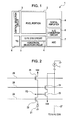
- Fig. 1 is a schematic structural view illustrating a rear surface irradiation type solid-state image pick-up device which is one example of a solid-state image pick-up device according to an embodiment of the present invention.
- a solid-state image pick-up device 1 of this embodiment has a pixel portion 2 and a peripheral circuit portion, and these portions are mounted on the same semiconductor substrate.
- the peripheral circuit portion includes a vertical selection circuit 3, a sample hold correlation double sampling (S/H ⁇ CDS) circuit 4, a horizontal selection circuit 5, a timing generator (TG) 6, an automatic gain control (AGC) circuit 7, an A/D converter circuit 8, and a digital amplifier 9.
- pixel portion 2 many unit pixels which will be described later are disposed in a matrix form, address lines and the like are provided on a row basis, and signal lines and the like are provided on a column basis.
- the vertical selection circuit 3 sequentially selects pixels on a row basis, and signals of individual pixels are read into the S/H ⁇ CDS circuit 4 for individual pixel columns through the vertical signal lines.
- the S/H ⁇ CDS circuit 4 performs a signal processing, such as correlated double sampling (CDS), on the pixel signals read from the individual pixel columns.
- CDS correlated double sampling
- the horizontal selection circuit 5 sequentially takes out the pixel signals held in the S/H ⁇ CDS circuit 4 and output the pixel signals to the AGC circuit 7.
- the AGC circuit 7 amplifies the signals input from the horizontal selection circuit 5 with an appropriate gain and outputs the amplified signals to the A/D converter circuit 8.
- the A/D converter circuit 8 converts the analog signals input from the AGC circuit 7 into digital signals and outputs the digital signals to the digital amplifier 9.
- the digital amplifier 9 appropriately amplifies the digital signals input from the A/D converter circuit 8 and outputs the amplified digital signals to pads (terminals).
- the operations of the vertical selection circuit 3, the S/H ⁇ CDS circuit 4, the horizontal selection circuit 5, the AGC circuit 7, the A/D converter circuit 8, and the digital amplifier 9 are performed based on various types of timing signals output from the timing generator 6.
- Fig. 2 is a schematic view illustrating one example of a circuit structure of a unit pixel of the pixel portion 2.
- the unit pixel includes, for example, a photodiode 21 as a photoelectric conversion element, and in addition, four transistors, that is, a transfer transistor 22, an amplifying transistor 23, an address transistor 24, and a reset transistor 25, are also included as active elements for this one photodiode 21.
- the photodiode 21 performs photoelectric conversion of incident light into charges (electrons in this case) in an amount corresponding to the amount of the incident light.
- the transfer transistor 22 is connected between the photodiode 21 and a floating diffusion FD.
- a drive signal is supplied to the gate (transfer gate) of the transfer transistor 22 through a drive wire 26, electrons which are photoelectric-converted by the photodiode 21 are transferred to the floating diffusion FD.
- the gate of the amplifying transistor 23 is connected to the floating diffusion FD.
- the amplifying transistor 23 is connected to a vertical signal line 27 through the address transistor 24 and forms a source follower with a constant current power source I located outside the pixel portion.
- an address signal is supplied to the gate of the address transistor 24 through a drive wire 28, and the address transistor 24 is turned on thereby, the amplifying transistor 23 amplifies the potential of the floating diffusion FD and outputs a voltage corresponding to the amplified potential to the vertical signal line 27.
- the voltage output from each pixel through the vertical signal line 27 is output to the S/H ⁇ CDS circuit 4.
- the reset transistor 25 is connected between a power source Vdd and the floating diffusion FD.
- a reset signal is supplied to the gate of the reset transistor 25 through a drive wire 29, the potential of the floating diffusion FD is reset to a power source potential Vdd. Since the gates of the transfer transistors 22, the gates of the address transistors 24, and the gates of the reset transistors 25 are respectively connected to each other in each row unit, the operations described above are simultaneously carried out for the pixels in one row.
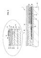
- Fig. 3 is a schematic cross-sectional view illustrating the rear surface irradiation type solid-state image pick-up device 1 which is one example of the solid-state image pick-up device according to an embodiment of the present invention.
- a surface (hereinafter referred to as a "rear surface” of a semiconductor substrate main body) opposite to a surface (hereinafter referred to as a "surface” of the semiconductor substrate main body) on which a wiring layer 38 is formed receives light.
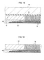
- the solid-state image pick-up device 1 shown in Fig. 3 is primarily formed of a semiconductor support substrate 31, a semiconductor substrate main body 32, a hafnium oxide film 34, a passivation film 35, a color filter 36, and a microlens 37.
- a shading film 13 the passivation film 35, the color filter 36, and the microlens 37, which are provided over the hafnium oxide film 34, are shown.
- the semiconductor substrate main body 32 is formed of n-type silicon.
- the semiconductor substrate main body 32 has an element forming layer 39 in which a plurality of light receiving portions 15 and active elements (not shown), such as MOS transistors, which convert signal charges photoelectric-converted by the light receiving portions into electrical signals and output these electrical signals, and the light receiving portions 15 and the active elements form the unit pixels.
- a gettering layer 33 is formed on the element forming layer 39 at a light incident side (rear surface side of the semiconductor substrate main body).
- the light receiving portion 15 corresponds to the photodiode 21 shown in Fig. 2 and is formed by a pn junction in the semiconductor substrate main body 32.
- the semiconductor substrate main body 32 is formed by decreasing the thickness of a silicon wafer so as to make light incident from the rear surface.
- the thickness of the semiconductor substrate main body 32 changes depending on the type of solid-state image pick-up device, the thickness thereof is 2 to 6 ⁇ m for visible light use and is 6 to 10 ⁇ m for infrared use.
- the wiring layer 38 which performs multilayer electrical wiring of the active elements, such as MOS transistors, is formed on the surface of the semiconductor substrate main body 32.
- the semiconductor support substrate 31 is adhered to the wiring layer 38 with a silicon dioxide layer 10 interposed therebetween.
- the semiconductor support substrate 31 is provided to reinforce the strength of the semiconductor substrate main body 32 and is formed, for example, of a silicon substrate, and the thickness thereof is, for example, approximately 725 ⁇ m.
- the hafnium oxide film 34 is formed on the rear surface of the semiconductor substrate main body 32.
- the hafnium oxide film 34 is one example of a dielectric film and places the surface of the gettering layer 33 and its vicinity in a positive charge accumulation state.
- the shading film 13 which has visible light incident apertures 12 in regions corresponding to the light receiving portions is formed on the hafnium oxide film 34, and the passivation film 35 is formed on the shading film 13.
- the color filter 36 and the microlens 37 are formed in a region corresponding to the visible light incident aperture 12.
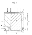
- Fig. 4 is a cross-sectional view of an important part of the pixel portion of the semiconductor substrate main body 32.
- an n-type charge accumulation region 41 is formed in the semiconductor substrate main body 32.
- the charge accumulation region 41 is preferably formed so that the impurity concentration is gradually increased toward the surface side of the semiconductor substrate main body 32.
- the charge accumulation region 41 may be formed so that the area thereof is gradually increased toward the rear surface side of the semiconductor substrate main body 32.
- a p-type well 42 is formed around the charge accumulation region 41.
- a shallow p-type hole accumulation region 44 is formed in the semiconductor substrate main body 32 at the surface side.
- an element isolation insulating film 40 made of silicon oxide is formed in the semiconductor substrate main body 32 at the surface side. Furthermore, an n-type floating diffusion (FD) 45 is formed in the semiconductor substrate main body 32 at the surface side.
- a p-type region 46 is formed between the floating diffusion 45 and the charge accumulation region 41, and hence they are electrically isolated from each other.
- the gettering layer 33 is formed on the entire surface of the element forming layer 39 by way of example.
- the gettering layer 33 can suppress metal contamination, which is caused by heave metals, of devices (such as photodiodes) formed in the element forming layer 39.
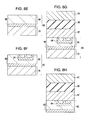
- the gettering layer 33 may not be necessarily formed on the entire surface of the element forming layer 39, and as shown in Fig. 6A , the gettering layer 33 may be partially formed on the element forming layer 39 at the incident light side (the rear surface side of the semiconductor substrate main body).
- the gettering layer 33 is preferably formed on the entire surface of the element forming layer 39.
- gettering layer 33 is formed on the element forming layer 39 only at the light incident side (the rear surface side of the semiconductor substrate main body) is described by way of example.
- gettering portions 14 may also be formed in the element forming layer 39.
- the gettering portions 14 are formed in the element forming layer 39, in order to prevent adverse influences caused by the flow of electrons generated due to crystalline defects of the gettering portions 14 into the light receiving portion, the gettering portions 14 are each necessarily formed to ensure a predetermined distance from the light receiving portion.
- the hafnium oxide film 34 is formed on the entire surface of the semiconductor substrate main body 32 by way of example.
- the hafnium oxide film 34 places the surface of the gettering layer 33 and its vicinity in a positive charge accumulation state, and hence the hafnium oxide film 34 may not be necessarily formed over the entire surface of the semiconductor substrate main body 32.
- the hafnium oxide film 34 may also be partially formed on an upper layer of the gettering layer 33.
- the hafnium oxide film 34 is formed is described by way of example, since it is sufficient when the surface of the gettering layer 33 and its vicinity can be placed in a positive charge accumulation state, another film may also be used instead of the hafnium oxide film 34.
- an oxide insulating film made of an element selected from zirconium, aluminum, tantalum, titanium, yttrium, and lanthanide may also be used.
- the light receiving portion 15 (charge accumulation region 41) is an n-type region, in order to place the surface of the gettering layer 33 and its vicinity in a positive charge accumulation state, the hafnium oxide film 34 is formed on the upper layer of the gettering layer 33.
- the surface of the gettering layer 33 and its vicinity are preferably placed in a negative charge accumulation state; hence, a dielectric film which places the surface of the gettering layer 33 and its vicinity in a negative charge accumulation state is to be formed on the upper layer of the gettering layer 33.
- the positive voltage is, for example, a power source voltage (3.3 V or 2.7 V).
- the potential of the floating diffusion 45 is amplified by the amplifying transistor 23, and a voltage corresponding to the amplified potential is output to the vertical signal line 27.
- the charge accumulation period, the reading operation, and the reset operation are repeatedly performed.
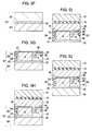
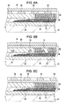
- the element isolation insulating film 40 is formed by a shallow trench isolation (STI) technique in the semiconductor substrate main body 32 which includes the element forming layer 39 and a thin film-forming removal layer 50.
- STI shallow trench isolation
- the formation order of the above regions is not particularly limited.
- the gettering layer 33 is formed between the element forming layer 39 and the thin film-forming removal layer 50.
- the implanted impurities are activated by a heat treatment using an arc lamp annealing device or the like, so that the gettering layer 33 is formed.
- the individual regions may be formed in the element forming layer 39 after the gettering layer 33 is formed.
- the gettering layer 33 is formed in such a way that after boron (B) ions or phosphorus (P) ions are implanted at a high energy, the heat treatment is performed using an arc lamp annealing device or the like, the method for forming the gettering layer 33 is not limited to that described above.
- the gettering layer 33 may be formed in such a way that after group IV ions, such as carbon ions or Si ions, are implanted, heat diffusion is performed at approximately 1,000 to 1,150°C.
- insulation films and wires are repeatedly formed on the surface of the semiconductor substrate main body 32, so that the wiring layer 38 is formed. Subsequently, the semiconductor support substrate 31 made of silicon is adhered to the wiring layer 38 with the silicon dioxide layer 10 interposed therebetween (see Fig. 5C ).
- the thin film-forming removal layer 50 is removed by a wet etching method, so that the gettering layer 33 is exposed. Since an impurity region which is heavily doped with impurities, such as boron (B) ions or phosphorus (P) ions, is able to function as an etching stopper, the gettering layer 33 functions as an etching stopper in the wet etching.
- impurities such as boron (B) ions or phosphorus (P) ions
- the hafnium oxide film 34 is formed on the rear surface of the semiconductor substrate main body 32 (see Figs. 5E ).
- the hafnium oxide film 34 is formed, for example, by an atomic layer deposition method. In addition, when the hafnium oxide film 34 is formed, a silicon oxide film (not shown) having a very small thickness is formed on the rear surface of the semiconductor substrate main body 32.
- the shading film 13 is formed on the hafnium oxide film 34, and a pattern processing is performed on the shading film 13 to form the visible light incident apertures 12 corresponding to the light receiving portions. Furthermore, the passivation film 35 is formed on the shading film 13 by a CVD method, and the color filters 36 and the microlenses 37 are also formed, so that the solid-state image pick-up device shown in Fig. 3 is obtained.
- Solid-state image pick-up devices comprising the semiconductor substrate main body 32 of a wafer level are separated into chips by dicing the wafer, and the chips thus separated are each processed by mounting, bonding, and sealing, so that the individual solid-state image pick-up devices can be formed.
- the gettering layer 33 is formed between the element forming layer 39 and the thin film-forming removal layer 50 of the semiconductor substrate main body 32.
- the implanted impurities are activated by a heat treatment using an arc lamp annealing device or the like, so that the gettering layer 33 is formed.
- the gettering layer 33 is formed in a wafer process.
- the gettering layer 33 is formed in a substrate manufacturing process which is performed before a wafer process.
- This method for forming the gettering layer 33 will be described with reference to a particular example.
- the semiconductor substrate main body 32 used for a solid-state image pick-up device is provided with an epitaxial film (not shown) thereon.
- the semiconductor substrate main body 32 provided with an epitaxial film grown thereon is variously processed in a wafer process.
- the gettering layer 33 is formed in a wafer process, after an epitaxial film is formed on the semiconductor substrate main body 32, the gettering layer 33 is formed.
- the gettering layer 33 in order to form the gettering layer 33 in a substrate manufacturing process, the gettering layer 33 is formed in the semiconductor substrate main body 32, and an epitaxial film is then formed on the semiconductor substrate main body 32.
- the element isolation insulating film 40 is formed by an STI technique in the element forming layer 39 of the semiconductor substrate main body 32.
- the n-type charge accumulation region 41, the p-type well 42, the p-type hole accumulation region 44, the floating diffusion 45, and the p-type region 46 are formed.
- the formation order of the above regions is not particularly limited.
- insulation films and wires are repeatedly formed on the surface of the semiconductor substrate main body 32, so that the wiring layer 38 is formed.
- the semiconductor support substrate 31 made of silicon is adhered to the wiring layer 38 with the silicon dioxide layer 10 interposed therebetween (see Fig. 5H ).
- the thin film-forming removal layer 50 is then removed by a wet etching method, so that the gettering layer 33 is exposed. Since an impurity region which is heavily doped with impurities, such as boron (B) ions or phosphorus (P) ions, is able to function as an etching stopper, the gettering layer 33 functions as an etching stopper in the wet etching.
- impurities such as boron (B) ions or phosphorus (P) ions
- the hafnium oxide film 34 is formed on the rear surface of the semiconductor substrate main body 32 (see Figs. 5J ).
- the hafnium oxide film 34 is formed, for example, by an atomic layer deposition method. In addition, when the hafnium oxide film 34 is formed, a silicon oxide film (not shown) having a very small thickness is formed on the rear surface of the semiconductor substrate main body 32.
- the shading film 13 is formed on the hafnium oxide film 34, and a pattern processing is performed on the shading film 13 to form the visible light incident apertures 12 corresponding to the light receiving portions. Furthermore, the passivation film 35 is formed on the shading film 13 by a CVD method, and the color filters 36 and the microlenses 37 are also formed, so that the solid-state image pick-up device shown in Fig. 3 is obtained.
- Solid-state image pick-up devices comprising the semiconductor substrate main body 32 of a wafer level are separated into chips by dicing the wafer, and the chips thus separated are each processed by mounting, bonding, and sealing, so that the individual solid-state image pick-up devices can be formed.
- the thin film-forming removal layer 50 is removed by etching using the gettering layer 33 as an etching stopper is described by way of example.
- a wet etching method may not be necessarily used as the method for removing the thin film-forming removal layer 50, and for example, the thin film-forming removal layer 50 may be removed by a mechanical polishing using a CMP method.
- the method for removing the thin film-forming removal layer 50 described above may be applied to both the manufacturing methods (1) and (2) of the solid-state image pick-up device according to an embodiment of the present invention.
- the gettering layer 33 is formed between the element forming layer 39 and the thin film-forming removal layer 50, and the thin film-forming removal layer 50 is then removed, so that the gettering layer 33 is exposed.
- the gettering layer 33 can be formed on the upper layer (incident light side) of the element forming layer 39, and hence the gettering layer 33 may be formed on the upper layer (incident light side) of the element forming layer 39 by using the semiconductor substrate main body 32 including no thin film-forming removal layer 50.
- the semiconductor substrate main body 32 including no thin film-forming removal layer 50 has a thickness of approximately 10 ⁇ m, it is believed that the handling of the semiconductor substrate main body 32 is considerably difficult in a manufacturing process.
- the thin film-forming removal layer 50 be removed.
- the method for forming the gettering layer 33 described above may be applied to both the manufacturing methods (1) and (2) of the solid-state image pick-up device according to an embodiment of the present invention.
- the gettering layer 33 since the gettering layer 33 is formed, metal contamination caused by heavy metals can be prevented in various processes after the thin film-forming removal layer 50 is removed.
- the hafnium oxide film 34 is formed on the upper layer of the gettering layer 33, electrons generated due to crystalline defects of the gettering layer 33 are suppressed from flowing into the light receiving portion.
- the hafnium oxide film 34 has a negative fixed charge therein, and because of this negative fixed charge, the surface of the gettering layer 33 and its vicinity are placed in a positive charge accumulation state.
- the electrons thus generated can be combined with holes in the region placed in the positive charge accumulation state, and as a result, the electrons are suppressed from flowing into the light receiving portion. Accordingly, noises of the solid-state image pick-up device are reduced, and the S/N ratio of the device can be improved.
- the degree of device design freedom can be increased, and the device characteristics can also be improved.
- a hole accumulation region which is a p-type region, is formed in the element forming layer at an incident light side (rear surface side of the semiconductor substrate main body).
- the hole accumulation region is formed as described above, the degree of device design freedom is decreased, and in addition, since the area for forming the light receiving portion is reduced, the device characteristics are degraded.
- the hole accumulation region may not be necessarily formed in the element forming layer 39, and as described above, the degree of device design freedom is increased, and the device characteristics can also be improved.
- the hafnium oxide film 34 also functions as an antireflection film, when the hafnium oxide film 34 is formed, an antireflection film may not be additionally formed.
- FIG. 7 is a schematic cross-sectional view illustrating one example of a semiconductor device according to an embodiment of the present invention.
- a semiconductor device 60 shown in this embodiment is, for example, RAM, ROM, or LSI and is primarily formed of a semiconductor support substrate 61, a semiconductor substrate main body 62, and a hafnium oxide film 63.
- the semiconductor substrate main body 62 is formed of n-type silicon.
- the semiconductor substrate main body 62 has an element forming layer 65 in which n-type devices 64, such as a logic element, an active element, and a passive element, are formed.
- n-type devices 64 such as a logic element, an active element, and a passive element, are formed.
- a gettering layer 66 is formed on the element forming layer 65.
- the thickness of the semiconductor substrate main body 62 changes depending on the type of semiconductor device, the thickness necessary for forming a device is approximately 10 ⁇ m.
- a wiring layer 67 performing multilayer electrical wiring of the devices 64 is formed on one surface (surface indicated by the mark A) of the semiconductor substrate main body 62.
- the semiconductor support substrate 61 is adhered to the wiring layer 67 with a silicon dioxide layer 68 interposed therebetween.
- the semiconductor support substrate 61 is provided to reinforce the strength of the semiconductor substrate main body 62 and is formed, for example, of a silicon substrate, and the thickness thereof is for example, approximately 725 ⁇ m.
- the hafnium oxide film 63 is formed on the other surface (surface indicated by the mark B) of the semiconductor substrate main body 62.
- the gettering layer 66 may not be necessarily formed on the entire surface of the element forming layer 65 and may be partially formed thereon. However, in consideration of the case in which the gettering layer 66 is used as an etching stopper in wet etching as describe later, the gettering layer 66 is preferably formed on the entire surface of the element forming layer 65.
- gettering portions may also be formed in the element forming layer 65 besides the gettering layer 66 formed on the element forming layer 65.
- the gettering portions are each necessarily formed to ensure a predetermined distance from the devices.
- the hafnium oxide film 63 may not be necessarily formed on the entire surface of the semiconductor substrate main body 62.
- another film may also be used instead of the hafnium oxide film 63.
- the hafnium oxide film 63 is formed on an upper layer of the gettering layer 66 in order to place the surface of the gettering layer 66 and its vicinity in a positive charge accumulation state.
- the devices 64 are each a p type, since the surface of the gettering layer 66 and its vicinity are necessarily placed in a negative charge accumulation state, a dielectric film which can place the surface of the gettering layer 66 and its vicinity in a negative charge accumulation region is formed on the upper layer of the gettering layer 66.
- the device 64 is formed in the semiconductor substrate main body 62 which includes the element forming layer 65 and a thin film-forming removal layer 70.
- the gettering layer 66 is formed between the element forming layer 65 and the thin film-forming removal layer 70.
- the implanted impurities are activated by a heat treatment using an arc lamp annealing device or the like, so that the gettering layer 66 is formed.
- the gettering layer 66 is formed is described by way of example, the device 64 may be formed in the element forming layer 65 after the gettering layer 66 is formed.
- the gettering layer 66 is formed in such a way that after boron (B) ions or phosphorus (P) ions are implanted at a high energy, the heat treatment is performed using an arc lamp annealing device or the like, the method for forming the gettering layer 66 is not limited to that described above.
- the gettering layer 66 may be formed in such a way that after group IV ions, such as carbon ions or Si ions, are implanted, heat diffusion is performed at approximately 1,000 to 1,150°C.
- insulation films and wires are repeatedly formed on one surface of the semiconductor substrate main body 62, so that the wiring layer 67 is formed. Subsequently, the semiconductor support substrate 61 made of silicon is adhered to the wiring layer 67 with the silicon dioxide layer 68 interposed therebetween (see Fig. 8C ).
- the thin film-forming removal layer 70 is removed by a wet etching method, so that the gettering layer 66 is exposed.
- the gettering layer 66 functions as an etching stopper.
- the hafnium oxide film 63 is formed on the other surface of the semiconductor substrate main body 62, so that the semiconductor device shown in Fig. 7 can be obtained.
- the hafnium oxide film 63 may be formed, for example, by an atomic layer deposition method.
- Semiconductor devices comprising the semiconductor substrate main body 62 of a wafer level are separated into chips by dicing the wafer, and the chips thus separated are each processed by mounting, bonding, and sealing, so that the individual semiconductor devices can be formed.
- the gettering layer 66 is formed between the element forming layer 65 and the thin film-forming removal layer 70 of the semiconductor substrate main body 62.
- the implanted impurities are activated by a heat treatment using an arc lamp annealing device or the like, so that the gettering layer 66 is formed.
- the gettering layer 66 is formed in a wafer process.
- the gettering layer 66 is formed in a substrate manufacturing process which is performed before a wafer process.
- This method for forming the gettering layer 66 will be described with reference to a particular example.
- the semiconductor substrate main body 62 used for a semiconductor device is provided with an epitaxial film (not shown) thereon.
- the semiconductor substrate main body 62 provided with an epitaxial film formed thereon is variously processed in a wafer process.
- the manufacturing method (1) of the semiconductor device according to an embodiment of the present invention in order to form the gettering layer 66 in a wafer process, after an epitaxial film is formed on the semiconductor substrate main body 62, the gettering layer 66 is formed.
- the gettering layer 66 in order to form the gettering layer 66 in a substrate manufacturing process, the gettering layer 66 is formed in the semiconductor substrate main body 62, and an epitaxial film is then formed on the semiconductor substrate main body 62.
- the device 64 is formed in the element forming layer 65 of the semiconductor substrate main body 62.
- insulation films and wires are repeatedly formed on one surface of the semiconductor substrate main body 62, so that the wiring layer 67 is formed.
- the semiconductor support substrate 61 made of silicon is then adhered to the wiring layer 67 with the silicon dioxide layer 68 interposed therebetween (see Fig. 8G ).
- the thin film-forming removal layer 70 is removed by a wet etching method, so that the gettering layer 66 is exposed.
- the gettering layer 66 functions as an etching stopper.
- the hafnium oxide film 63 is formed on the other surface of the semiconductor substrate main body 62, so that the semiconductor device shown in Fig. 7 can be obtained.
- the hafnium oxide film 63 may be formed, for example, by an atomic layer deposition method.
- Semiconductor devices comprising the semiconductor substrate main body 62 of a wafer level are separated into chips by dicing the wafer, and the chips thus separated are each processed by mounting, bonding, and sealing, so that the individual semiconductor devices can be formed.
- a wet etching method may not be necessarily used as the method for removing the thin film-forming removal layer 70.
- the thin film-forming removal layer 70 may be removed by mechanical polishing using a CMP method, and as in the first embodiment described above, this method may be applied to both the manufacturing methods (1) and (2) of the semiconductor device according to an embodiment of the present invention.
- the gettering layer 66 is formed, after the thin film-forming removal layer 70 is removed, metal contamination caused by heavy metals can be prevented in various processes.
- the hafnium oxide film 63 is formed on the upper layer of the gettering layer 66, electrons generated due to crystalline defects of the gettering layer 66 are suppressed from flowing into the device.
- the hafnium oxide film 63 has a negative fixed charge therein, and because of the negative fixed charge, the surface of the gettering layer 66 and its vicinity are placed in a positive charge accumulation state.
- the electrons thus generated can be combined with holes in the region placed in a positive charge accumulation state, and as a result, the electrons are suppressed from flowing into the device. Accordingly, noises of the semiconductor device are reduced.
- the degree of device design freedom can be increased, and the device characteristics can also be improved.
- the hole accumulation region which is a p-type region, is formed in the element forming layer.
- the hole accumulation region as described above is necessarily formed, the degree of device design freedom is decreased, and in addition, since the area for forming the device is reduced, the device characteristics are degraded.
- the hole accumulation region may not be necessarily formed in the element forming layer 65, and as described above, the degree of device design freedom is increased, and the device characteristics are also improved.
- Fig. 9 is a schematic view illustrating a camera 77 which is one example of an image pick-up apparatus according to an embodiment of the present invention.
- the camera 77 thus shown uses the solid-state image pick-up device according to the first embodiment described above as an image pick-up device.
- a solid-state image pick-up device 73 In the camera 77 using the solid-state image pick-up device according to the first embodiment of the present invention, light from an object (not shown) is incident on an image pick-up area of a solid-state image pick-up device 73 through an optical system, such as a lens 71, and a mechanical shutter 72.
- the mechanical shutter 72 blocks light incident on the image pick-up area of the solid-state image pick-up device 73 and determines an exposure time.
- the solid-state image pick-up device 1 is used as the solid-state image pick-up device 73, and the solid-state image pick-up device 73 is driven by a drive circuit 74 including a timing generation circuit and a drive system.
- an output signal of the solid-state image pick-up device 73 is processed by various signal processings by the following signal processing circuit 75 and is then sent outside as an image pick-up signal, and the image pick-up signal thus sent is stored in a recording medium, such as a memory, or is output to a monitor.
- the camera 77 described above uses the solid-state image pick-up device 1 according to the first embodiment of the present invention, metal contamination caused by heavy metals can be prevented in various processes, and hence a high-quality pickup image can be obtained.
- the hafnium oxide film 34 is formed on the upper layer of the gettering layer 33, electrons generated due to crystalline defects of the gettering layer 33 can be suppressed from flowing into the light receiving portion. Hence, noises of the solid-state image pick-up device can be reduced, and the S/N ratio of the device can be improved, so that a high-quality pickup image can be obtained.
- the device characteristics can be improved, and as a result, a high-quality pickup image can be obtained.
- the solid-state image pick-up device according to the first embodiment is used as an image pick-up device
- a solid-state image pick-up device according to the following fourth embodiment may also be used.
- a rear surface irradiation type solid-state image pick-up device 1 which is another example of the solid-state image pick-up device according to an embodiment of the present invention has the pixel portion 2 and the peripheral circuit portion, and these portions are mounted on the same semiconductor substrate.
- the peripheral circuit portion includes the vertical selection circuit 3, the S/H ⁇ CDS circuit 4, the horizontal selection circuit 5, the TG 6, the AGC circuit 7, the A/D converter circuit 8, and the digital amplifier 9 (see Fig. 1 ).
- pixel portion 2 many unit pixels are disposed in a matrix form, address lines and the like are provided on a row basis, and signal lines and the like are provided on a column basis.
- address lines and the like are provided on a row basis
- signal lines and the like are provided on a column basis.
- the structure described above is the same as that in the first embodiment.
- the vertical selection circuit 3 sequentially selects pixels on a row basis, and signals of individual pixels are read into the S/H ⁇ CDS circuit 4 for individual pixel columns through the vertical signal lines.
- the S/H ⁇ CDS circuit 4 performs a signal processing, such as CDS, on the pixel signals read from the individual pixel columns.
- CDS signal processing
- the horizontal selection circuit 5 sequentially takes out the pixel signals held in the S/H ⁇ CDS circuit 4 and output the pixel signals to the AGC circuit 7.
- the AGC circuit 7 amplifies the signals input from the horizontal selection circuit 5 with an appropriate gain and outputs the amplified signals to the A/D converter circuit 8.
- the structure described above is also the same as that in the first embodiment.
- the A/D converter circuit 8 converts the analog signals input from the AGC circuit 7 into digital signals and outputs the digital signals to the digital amplifier 9.
- the digital amplifier 9 appropriately amplifies the digital signals input from the A/D converter circuit 8 and outputs the amplified digital signals to pads (terminals).
- the structure described above is also the same as that in the first embodiment.
- the operations of the vertical selection circuit 3, the S/H ⁇ CDS circuit 4, the horizontal selection circuit 5, the AGC circuit 7, the A/D converter circuit 8, and the digital amplifier 9 are performed based on various types of timing signals output from the timing generator 6.
- the structure described above is also the same as that in the first embodiment.
- the unit pixel forming the pixel portion 2 includes, for example, the photodiode 21 as a photoelectric conversion element, and four transistors, that is, the transfer transistor 22, the amplifying transistor 23, the address transistor 24, and the reset transistor 25, are also included as active elements for this one photodiode 21 (see Fig. 2 ).
- the photodiode 21 performs photoelectric conversion of incident light into charges (electrons in this case) in an amount corresponding to the amount of the incident light.
- the transfer transistor 22 is connected between the photodiode 21 and the floating diffusion FD.
- a drive signal is supplied to the gate (transfer gate) of the transfer transistor 22 through the drive wire 26, electrons which are photoelectric-converted in the photodiode 21 are transferred to the floating diffusion FD.
- the gate of the amplifying transistor 23 is connected to the floating diffusion FD.
- the amplifying transistor 23 is connected to the vertical signal line 27 through the address transistor 24 and forms the source follower with the constant current power source I located outside the pixel portion.
- the amplifying transistor 23 amplifies the potential of the floating diffusion FD and outputs a voltage corresponding to the amplified potential to the vertical signal line 27.
- the voltage output from each pixel through the vertical signal line 27 is output to the S/H ⁇ CDS circuit 4.
- the reset transistor 25 is connected between the power source Vdd and the floating diffusion FD.
- a reset signal is supplied to the gate of the reset transistor 25 through the drive wire 29, the potential of the floating diffusion FD is reset to the power source potential Vdd. Since the gates of the transfer transistors 22, the gates of the address transistors 24, and the gates of the reset transistors 25 are respectively connected to each other in each row unit, the operations described above are simultaneously carried out for the pixels in one row.
- the structure described above is also the same as that in the first embodiment.
- Fig. 10 is a schematic cross-sectional view illustrating the rear surface irradiation type solid-state image pick-up device which is another example of the solid-state image pick-up device according to an embodiment of the present invention.
- the solid-state image pick-up device 1 shown in Fig. 10 is primarily formed of the semiconductor support substrate 31, the semiconductor substrate main body 32, the passivation film 35, the color filter 36, and the microlens 37.
- the shading film 13 the passivation film 35, the color filter 36, and the microlens 37, which are provided over the semiconductor substrate main body 32, are shown.
- the semiconductor substrate main body 32 is formed of n-type silicon.
- the semiconductor substrate main body 32 has the element forming layer 39 in which a plurality of the light receiving portions 15 and active elements (not shown), such as MOS transistors, which convert signal charges photoelectric-converted by the light receiving portions into electrical signals and output these electrical signals are formed, and the light receiving portions 15 and the active elements form the unit pixels.
- a p + layer 84 which is an impurity region is formed on the element forming layer 39 at a light incident side (rear surface side of the semiconductor substrate main body), and a gettering layer 83 is formed on the p + layer 84 at a light incident side (rear surface side of the semiconductor substrate main body).
- the light receiving portion 15 corresponds to the photodiode 21 shown in Fig. 2 and is formed of a pn junction in the semiconductor substrate main body 32.
- the p + layer 84 is one example of a second conductive type impurity region.
- the semiconductor substrate main body 32 is formed by decreasing the thickness of a silicon wafer so as to make light incident from the rear surface.
- the thickness of the semiconductor substrate main body 32 changes depending on the type of solid-state image pick-up device, the thickness thereof is 2 to 6 ⁇ m for visible light use and is 6 to 10 ⁇ m for infrared use.
- the wiring layer 38 performing multilayer electrical wiring of the active elements, such as MOS transistors, is formed on the surface of the semiconductor substrate main body 32.
- the semiconductor support substrate 31 is adhered to the wiring layer 38 with the silicon dioxide layer 10 interposed therebetween.
- the semiconductor support substrate 31 is provided to reinforce the strength of the semiconductor substrate main body 32 and is formed, for example, of a silicon substrate, and the thickness thereof is, for example, approximately 725 ⁇ m.
- the shading film 13 which has the visible light incident apertures 12 in regions corresponding to the light receiving portions is formed on an upper layer of the semiconductor substrate main body 32, and the passivation film 35 is formed on an upper layer of the shading film 13.
- the color filter 36 and the microlens 37 are formed in a region corresponding to the visible light incident aperture 12.
- Fig. 11 is a cross-sectional view showing an important part of the pixel portion of the semiconductor substrate main body 32.
- the n-type charge accumulation region 41 is formed in the semiconductor substrate main body 32.
- the charge accumulation region 41 is preferably formed so that the impurity concentration is gradually increased toward the surface side of the semiconductor substrate main body 32.
- the charge accumulation region 41 may be formed so that the area thereof is gradually increased toward the rear surface side of the semiconductor substrate main body 32.
- the p-type well 42 is formed around the charge accumulation region 41.
- the shallow p-type hole accumulation region 44 is formed in the semiconductor substrate main body 32 at the surface side.
- the element isolation insulating film 40 made of silicon oxide is formed in the semiconductor substrate main body 32 at the surface side. Furthermore, the n-type floating diffusion (FD) 45 is formed in the semiconductor substrate main body 32 at the surface side.
- the p-type region 46 is formed between the floating diffusion 45 and the charge accumulation region 41, and hence they are electrically isolated from each other.
- the gettering layer 83 is formed on the entire surface of the p + layer 84 in this fourth embodiment.
- the gettering layer 83 can suppress metal contamination, which is caused by heavy metals, of a device (such as a photodiode) formed in the element forming layer 39.
- the gettering layer 83 may not be necessarily formed on the entire surface of the p + layer 84 and may be partially formed at the incident light side (the rear surface side of the semiconductor substrate main body) of the element forming layer 39.
- the gettering layer 83 is preferably formed on the entire surface of the p + layer 84.
- the gettering layer 83 is formed only at the light incident side (the rear surface side of the semiconductor substrate main body) of the element forming layer 39 is described by way of example.
- the gettering portions may also be formed in the element forming layer 39.
- the gettering portions are formed in the element forming layer 39, in order to prevent adverse influences caused by the flow of electrons generated due to crystalline defects of the gettering portions into the light receiving portion, the gettering portions are each necessarily formed to ensure a predetermined distance from the light receiving portion.
- the case in which the p + layer 84 is formed on the entire surface of the element forming layer 39 is described by way of example. However, it is sufficient when the p + layer 84 is provided in the vicinity of the light receiving portion 15, and hence the p + layer 84 may not be necessarily formed on the entire surface of the element forming layer 39.
- the p + layer 84 which is a p-type impurity region, is formed.
- an n + layer which is an n + -type impurity region, is to be formed.
- the positive voltage is, for example, a power source voltage (3.3 V or 2.7 V).
- the potential of the floating diffusion 45 is amplified by the amplifying transistor 23, and a voltage corresponding to the amplified potential is output to the vertical signal line 27.
- the charge accumulation period, the reading operation, and the reset operation are repeatedly performed.
- the element isolation insulating film 40 is formed by a STI technique in the semiconductor substrate main body 32 which includes the element forming layer 39 and the thin film-forming removal layer 50.
- the n-type charge accumulation region 41, the p-type well 42, the p-type hole accumulation region 44, the floating diffusion 45, and the p-type region 46 are formed.
- the formation order of the above regions is not particularly limited.
- the p + layer 84 is formed in the element forming layer 39 at a side of the thin film-forming removal layer 50.
- phosphorus (P) ions are implanted at a high energy, so that the p + layer 84 is formed.
- the gettering layer 83 is formed in the p + layer 84 at the thin film-forming removal layer 50 side.
- the implanted impurities are activated by a heat treatment using an arc lamp annealing device or the like, so that the gettering layer 83 is formed.
- the individual regions may be formed in the element forming layer 39 after the p + layer 84 and the gettering layer 83 are formed.
- the gettering layer 83 is formed is described by way of example, the p + layer 84 may be formed after the gettering layer 83 is formed.
- the gettering layer 83 is formed in such a way that after boron (B) ions or phosphorus (P) ions are implanted at a high energy, the heat treatment is performed using an arc lamp annealing device or the like, the method for forming the gettering layer 83 is not limited to that described above.
- the gettering layer 83 may be formed in such a way that after group IV ions, such as carbon ions or Si ions, are implanted, heat diffusion is performed at approximately 1,000 to 1,150°C.
- insulation films and wires are repeatedly formed on the surface of the semiconductor substrate main body 32, so that the wiring layer 38 is formed. Subsequently, the semiconductor support substrate 31 made of silicon is adhered to the wiring layer 38 with the silicon dioxide layer 10 interposed therebetween (see Fig. 12C ).
- the thin film-forming removal layer 50 is removed by a wet etching method, so that the gettering layer 83 is exposed. Since an impurity region which is heavily doped with impurities, such as boron (B) ions or phosphorus (P) ions, is able to function as an etching stopper, the gettering layer 83 functions as an etching stopper in the wet etching.
- impurities such as boron (B) ions or phosphorus (P) ions
- the shading film 13 is formed on the semiconductor substrate main body 32, and a pattern processing is performed on the shading film 13 to form the visible light incident apertures 12 corresponding to the light receiving portions. Furthermore, the passivation film 35 is formed on the shading film 13 by a CVD method, and the color filters 36 and the microlenses 37 are also formed, so that the solid-state image pick-up device shown in Fig. 10 can be obtained.
- Solid-state image pick-up devices comprising the semiconductor substrate main body 32 of a wafer level are separated into chips by dicing the wafer, and the chips thus separated are each processed by mounting, bonding, and sealing, so that the individual solid-state image pick-up devices can be formed.
- the gettering layer 83 is formed between the element forming layer 39 and the thin film-forming removal layer 50 of the semiconductor substrate main body 32.
- the implanted impurities are activated by a heat treatment using an arc lamp annealing device or the like, so that the gettering layer 83 is formed.
- the gettering layer 83 is formed in a wafer process.
- the gettering layer 83 is formed in a substrate manufacturing process which is performed before a wafer process.
- This method for forming the gettering layer 83 will be described with reference to a particular example.
- the semiconductor substrate main body 32 used for a solid-state image pick-up device is provided with an epitaxial film (not shown) thereon.
- the semiconductor substrate main body 32 provided with an epitaxial film grown thereon is variously processed in a wafer process.
- the gettering layer 83 is formed in a wafer process, after an epitaxial film is formed on the semiconductor substrate main body 32, the gettering layer 83 is formed.
- the gettering layer 83 is formed in a substrate manufacturing process, the gettering layer 83 is formed in the semiconductor substrate main body 32, and an epitaxial film is then formed on the semiconductor substrate main body 32.
- the element isolation insulating film 40 is formed by a STI technique in the element forming layer 39 of the semiconductor substrate main body 32.
- the n-type charge accumulation region 41, the p-type well 42, and the p-type hole accumulation region 44, the floating diffusion 45, and the p-type region 46 are formed.
- the formation order of the above regions is not particularly limited.
- the p + layer 84 is formed between the element forming layer 39 and the gettering layer 83.
- the p + layer 84 is formed, for example, by implanting phosphorus (P) ions at a high energy.
- the individual regions are formed in the element forming layer 39, and the p + layer 84 is then formed is described by way of example, after the p + layer 84 is formed, the individual regions may be formed in the element forming layer 39.
- insulation films and wires are repeatedly formed on the surface of the semiconductor substrate main body 32, so that the wiring layer 38 is formed. Subsequently, the semiconductor support substrate 31 made of silicon is adhered to the wiring layer 38 with the silicon dioxide layer 10 interposed therebetween (see Fig. 12G ).
- the thin film-forming removal layer 50 is removed by a wet etching method, so that the gettering layer 83 is exposed. Since an impurity region which is heavily doped with impurities, such as boron (B) ions or phosphorus (P) ions, is able to function as an etching stopper, the gettering layer 83 functions as an etching stopper in the wet etching.
- impurities such as boron (B) ions or phosphorus (P) ions
- the shading film 13 is formed on the semiconductor substrate main body 32, and a pattern processing is performed on the shading film 13 to form the visible light incident apertures 12 corresponding to the light receiving portions. Furthermore, the passivation film 35 is formed on the shading film 13 by a CVD method, and the color filters 36 and the microlenses 37 are also formed, so that the solid-state image pick-up device shown in Fig. 10 can be obtained.
- Solid-state image pick-up devices comprising the semiconductor substrate main body 32 of a wafer level are separated into chips by dicing the wafer, and the chips thus separated are each processed by mounting, bonding, and sealing, so that the individual solid-state image pick-up devices can be formed.
- the gettering layer 83 is used as an etching stopper, and the thin film-forming removal layer 50 is removed by etching using a wet etching method is described by way of example.
- a wet etching method may not be necessarily used as the method for removing the thin film-forming removal layer 50, and for example, the thin film-forming removal layer 50 may be removed by a mechanical polishing using a CMP method.
- the method for removing the thin film-forming removal layer 50 described above may be applied to both the manufacturing methods (3) and (4) of the solid-state image pick-up device according to an embodiment of the present invention.
- the p + layer 84 and the gettering layer 83 are formed between the element forming layer 39 and the thin film-forming removal layer 50, and the thin film-forming removal layer 50 is then removed, so that the gettering layer 83 is exposed.
- the p + layer 84 and the gettering layer 83 can be formed on the upper layer (incident light side) of the element forming layer 39.
- the p + layer 84 and the gettering layer 83 may be formed on the upper layer (incident light side) of the element forming layer 39.
- the semiconductor substrate main body 32 having no thin film-forming removal layer 50 has a thickness of approximately 10 ⁇ m, it is believed that the handling of the semiconductor substrate main body 32 becomes considerably difficult in a manufacturing process.
- the semiconductor substrate main body 32 including the thin film-forming removal layer 50 the thin film-forming removal layer 50 is preferably removed after the semiconductor support substrate 31 is adhered to the wiring layer 38.
- the use of the thin film-forming removal layer described above may be applied to both the manufacturing methods (3) and (4) of the solid-state image pick-up device according to an embodiment of the present invention.
- the gettering layer 83 is formed, after the thin film-forming removal layer 50 is removed, metal contamination caused by heavy metals can be prevented in various processes.
- the p + layer 84 is formed, electrons generated due to crystalline defects of the gettering layer 83 are suppressed from flowing into the light receiving portion.
- the electrons thus generated can be combined with holes in the p + layer 84, and as a result, the electrons are suppressed from flowing into the light receiving portion. Accordingly, noises of the solid-state image pick-up device are reduced, and the S/N ratio of the device can be improved.
- Fig. 13 is a schematic cross-sectional view illustrating another example of the semiconductor device according to an embodiment of the present invention.
- the semiconductor device 60 shown in this embodiment is, for example, RAM, ROM, or LSI and is primarily formed of the semiconductor support substrate 61 and the semiconductor substrate main body 62.
- the semiconductor substrate main body 62 is formed of n-type silicon.
- the semiconductor substrate main body 62 has the element forming layer 65 in which the n-type devices 64, such as a logic element, an active element, and a passive element, are formed.
- a p + layer 93 which is an impurity region, is formed on the element forming layer 65, and a gettering layer 96 is formed on the p + layer 93.
- the thickness of the semiconductor substrate main body 62 changes depending on the type of semiconductor device, the thickness necessary for forming a device is approximately 10 ⁇ m.
- the p + layer 93 is one example of a second conductive type impurity region.
- the wiring layer 67 performing multilayer electrical wiring of the devices 64 is formed on one surface (surface indicated by the mark A) of the semiconductor substrate main body 62.
- the semiconductor support substrate 61 is adhered to the wiring layer 67 with the silicon dioxide layer 68 interposed therebetween.
- the semiconductor support substrate 61 is provided to reinforce the strength of the semiconductor substrate main body 62 and is formed, for example, of a silicon substrate, and the thickness thereof is, for example, approximately 725 ⁇ m.
- the gettering layer 96 may not be necessarily formed on the entire surface of the p + layer 93 and may be partially formed thereon. However, in consideration of the case in which the gettering layer 96 is used as an etching stopper in wet etching as describe later, the gettering layer 96 is preferably formed on the entire surface of the p + layer 93.
- the gettering portions may also be formed in the element forming layer 65 besides the gettering layer 96 formed above the element forming layer 65.
- the gettering portions are each necessarily formed to ensure a predetermined distance from the devices.
- the p + layer 93 which is a p + -type impurity region, is formed.
- an n + layer which is an n + -type impurity region, is to be formed.
- the device 64 is formed in the semiconductor substrate main body 62 which includes the element forming layer 65 and the thin film-forming removal layer 70.
- the p + layer 93 is formed in the element forming layer 65 at a side of the thin film-forming removal layer 70.
- phosphorous (P) ions are implanted at a high energy, so that the p + layer 93 is formed.
- the gettering layer 96 is formed in the p + layer 93 at the thin film-forming removal layer 70 side.
- the implanted impurities are activated by a heat treatment using an arc lamp annealing device or the like, so that the gettering layer 96 is formed.
- the device 64 may be formed in the element forming layer 65 after the p + layer 93 and the gettering layer 96 are formed.
- the gettering layer 96 is formed is described by way of example, after the gettering layer 96 is formed, the p + layer 93 may be formed.
- the gettering layer 96 is formed in such a way that after boron (B) ions or phosphorus (P) ions are implanted at a high energy, the heat treatment is performed using an arc lamp annealing device or the like, the method for forming the gettering layer 96 is not limited to that described above.
- the gettering layer 96 may be formed in such a way that after group IV ions, such as carbon ions or Si ions, are implanted, heat diffusion is performed at approximately 1,000 to 1,150°C.
- insulation films and wires are repeatedly formed on one surface of the semiconductor substrate main body 62, so that the wiring layer 67 is formed. Subsequently, the semiconductor support substrate 61 made of silicon is adhered to the wiring layer 67 with the silicon dioxide layer 68 interposed therebetween (see Fig. 14C ).
- the thin film-forming removal layer 70 is removed by a wet etching method to expose the gettering layer 96, so that the semiconductor device shown in Fig. 13 can be obtained.
- the gettering layer 96 functions as an etching stopper.
- Semiconductor devices comprising the semiconductor substrate main body 62 of a wafer level are separated into chips by dicing the wafer, and the chips thus separated are each processed by mounting, bonding, and sealing, so that the individual semiconductor devices can be formed.
- the gettering layer 96 is formed between the element forming layer 65 and the thin film-forming removal layer 70 of the semiconductor substrate main body 62.
- the implanted impurities are activated by a heat treatment using an arc lamp annealing device or the like, so that the gettering layer 96 is formed.
- the gettering layer 96 is formed in a wafer process.
- the gettering layer 96 is formed in a substrate manufacturing process which is performed before a wafer process.
- This method for forming the gettering layer 96 will be described with reference to a particular example.
- the semiconductor substrate main body 62 used for a semiconductor device is provided with an epitaxial film (not shown) thereon.
- the semiconductor substrate main body 62 provided with an epitaxial film grown thereon is variously processed in a wafer process.
- the gettering layer 96 is formed in a wafer process, after an epitaxial film is formed on the semiconductor substrate main body 62, the gettering layer 96 is formed.
- the gettering layer 96 is formed in a substrate manufacturing process, the gettering layer 96 is formed in the semiconductor substrate main body 62, and an epitaxial film is then formed thereon.
- the device 64 is formed in the element forming layer 65 of the semiconductor substrate main body 62.
- insulation films and wires are repeatedly formed on one surface of the semiconductor substrate main body 62, so that the wiring layer 67 is formed.
- the semiconductor support substrate 61 made of silicon is adhered to the wiring layer 67 with the silicon dioxide layer 68 interposed therebetween (see Fig. 14G ).
- the thin film-forming removal layer 70 is removed by a wet etching method to expose the gettering layer 96, so that the semiconductor device shown in Fig. 13 can be obtained.
- Semiconductor devices comprising the semiconductor substrate main body 62 of a wafer level are separated into chips by dicing the wafer, and the chips thus separated are each processed by mounting, bonding, and sealing, so that the individual semiconductor devices can be formed.
- a wet etching method may not be necessarily used, and for example, the thin film-forming removal layer 70 may be removed by mechanical polishing using a CMP method.
- the above method for removing the thin film-forming removal layer 70 may be applied to both the manufacturing methods (3) and (4) of the semiconductor device according to an embodiment of the present invention.
- the gettering layer 96 is formed, after the thin film-forming removal layer 70 is removed, metal contamination caused by heavy metals can be prevented in various processes.
- the p + layer 93 is formed, electrons generated due to crystalline defects of the gettering layer 96 are suppressed from flowing into the device.
- the electrons can be combined with holes of the p + layer 93, and as a result, electrons are suppressed from flowing into the device. Accordingly, noises of the semiconductor device are reduced.
Abstract
Description
- The present invention relates to a solid-state image pick-up device and a manufacturing method thereof; an image pick-up apparatus; a semiconductor device and a manufacturing method thereof; and a semiconductor substrate. In more particular, the present invention relates to a solid-state image pick-up device in which a gettering layer is provided on an upper layer of an element forming layer to suppress metal contamination and a manufacturing method of the solid-state image pick-up device; an image pick-up apparatus; a semiconductor device and a manufacturing method thereof; and a semiconductor substrate.
- A thin semiconductor device having a high strength, such as a rear surface irradiation type solid-state image pick-up device, has an element forming layer and a wiring layer provided on one surface of the element forming layer. In the element forming layer, photoelectric conversion elements and active elements are formed, and the active elements convert signal charges which are photoelectric-converted by the photoelectric conversion elements into electrical signals and output the electrical signals. In addition, the wiring layer performs wiring of the active elements formed in the element forming layer. Furthermore, it is configured such that visible light is incident on the photoelectric conversion elements from one surface of the element forming layer located at a side opposite to that of the wiring layer (see for example, Japanese Unexamined Patent Application Publication No.
2003-31785 - In order to optimize the spectral balance of color to the photoelectric conversion element when visible light is converted into an electrical signal and also to form a pixel having a desired device structure from a front surface side to a rear surface side, the element forming layer is preferably formed to have a desired small thickness. For example, in the case of a solid-state image pick-up device in which a silicon substrate is used as the element forming layer, the thickness thereof is preferably decreased to 10 µm or less.
- As a semiconductor substrate in which elements, such as photoelectric conversion elements and active elements, are formed in a three-dimensional manner, in general, a silicon substrate having an SOI structure is used in which an element forming layer (SOI layer) made of silicon is formed on a silicon substrate functioning as a support substrate with a SiO2 film (BOX layer) interposed therebetween.
- Next, with reference to
Figs. 15 and 16 , a related example will be described in which a rear surface irradiation type solid-state image pick-up device is formed using a semiconductor substrate which has an SOI structure. - As shown in
Fig. 15 , a silicon oxide film (SiO2) 102 having a thickness of approximately 1 µm is formed on a surface of asilicon substrate 101 functioning as a support substrate, and anelement forming layer 103 having an SOI structure is formed on thesilicon oxide film 102. In addition, in theelement forming layer 103, there are formedphotoelectric conversion elements 104 and active elements (not shown) which convert signal charges photoelectric-converted by the photoelectric conversion elements into electrical signals and which output the above signals. Furthermore, awiring layer 105 which performs wiring of the active elements is formed on the surface of theelement forming layer 103. - In the semiconductor substrate of the solid-state image pick-up device described above, after the elements are formed in the
element forming layer 103, and thewiring layer 105 is formed, as shown inFig. 16 , the thickness of the semiconductor substrate is decreased from a rear surface side (visible light incident side), so that only theelement forming layer 103 is allowed to remain. - In the semiconductor structure having an SOI structure described above, the
silicon oxide film 102 is formed in the semiconductor substrate. Hence, when the thickness of the semiconductor substrate is decreased by wet etching, the etching can be stopped by thesilicon oxide film 102. In addition, when thesilicon oxide film 102 is subsequently peeled away, only theelement forming layer 103 may be allowed to remain. - However, a method for manufacturing a semiconductor substrate including a different type of material (SiO2), such as a semiconductor substrate having an SOI structure, is complicated, and the product obtained by the method described above is expensive. In addition, since a gettering layer is not formed in the
element forming layer 103, after thesilicon oxide film 102 is removed, it is difficult to prevent metal contamination caused by heavy metals in various processes. - In addition, heretofore, a technique has been proposed in which a structure having a gettering effect against metal contamination is formed in a semiconductor substrate at a rear surface side (for example, see Japanese Unexamined Patent Application Publication No.
6-61235 - However, in the case in which an insulating film is present in a substrate as in a semiconductor substrate having an SOI structure, since the insulating film prevents the diffusion of metals, even when the gettering effect is imparted to a rear surface side of the semiconductor substrate having an SOI structure, the gettering effect described above may not be sufficiently obtained. In addition, in the case in which the thickness of the semiconductor substrate is decreased from a rear surface side thereof so that only an SOI layer is allowed to remain, the gettering layer formed in the semiconductor substrate at a rear surface side is also removed, and hence in a process after the gettering layer is removed, no gettering effect can be obtained.
- In addition, another technique is also conceived in which a gettering layer is formed in a deep region of an SOI layer which is close to a BOX layer. However, when the gettering layer is provided in a deep region of the SOI layer, in the case in which elements are formed not only in a surface region of the SOI layer but also in a region thereof in a depth direction, degradation in element characteristics caused by crystalline defects derived from the gettering layer may occur in some cases.
- Accordingly, in order to prevent metal contamination and to suppress the degradation in element characteristics, a technique has been proposed in which a gettering layer is provided between an element forming layer in which elements are formed and a thin film-forming removal layer laminated on one surface of the element forming layer (see for example, Japanese Unexamined Patent Application Publication No.
2007-88450 - However, electrons and the like generated due to the presence of the gettering layer may cause noises in some cases. That is, in general, the gettering layer is a defective layer formed in a silicon single crystal, and even when a silicon substrate is metal-contaminated, the defective layer collects metals using heat generated in a wafer process. Hence, the influence of contamination can be suppressed in a silicon substrate in which elements are formed. However, since the gettering layer is formed from a defective layer, electrons and the like generated therefrom as described above may adversely cause noises in some cases. Hence, as described above, it is believed that electrons and the like generated due to the presence of the gettering layer may cause noises.
- The present invention has been conceived in consideration of the problems described above, and it is desirable to provide a solid-state image pick-up device which can suppress noises generated due to the presence of a gettering layer and a manufacturing method of the solid-state image pick-up device; an image pick-up apparatus; a semiconductor device and a manufacturing method thereof; and a semiconductor substrate.
- According to an embodiment of the present invention, there is provided a solid-state image pick-up device which includes a semiconductor substrate main body which includes an element forming layer and a gettering layer provided on an upper layer thereof; photoelectric conversion elements, each of which includes a first conductive type region, provided in the element forming layer; and a dielectric film which is provided on an upper layer of the gettering layer and which induces a second conductive type region in a surface of the gettering layer.
- According to an embodiment of the present invention, there is provided an image pick-up apparatus which includes a solid-state image pick-up device including a semiconductor substrate main body which has an element forming layer and a gettering layer provided on an upper layer thereof; photoelectric conversion elements, each of which includes a first conductive type region, formed in the element forming layer; and a dielectric film which is provided on an upper layer of the gettering layer and which induces a second conductive type region in a surface of the gettering layer; an optical system for guiding incident light from an object to the solid-state image pick-up device; and a signal processing circuit for processing an output signal from the solid-state image pick-up device.
- In addition, according to an embodiment of the present invention, there is provided a semiconductor device which includes: a semiconductor substrate main body which includes an element forming layer and a gettering layer provided on an upper layer of the element forming layer; a device which includes a first conductive type region and is formed in the element forming layer; and a dielectric film which is provided on an upper layer of the gettering layer and which induces a second conductive type region in a surface of the gettering layer.
- In addition, according to an embodiment of the present invention, there is provided a semiconductor substrate which includes: a semiconductor substrate main body which includes an element forming layer in which a device including a first conductive type region is provided and a gettering layer provided on an upper layer of the element forming layer; and a dielectric film which is provided on an upper layer of the gettering layer and which induced a second conductive type region in a surface of the gettering layer.
- Since the second conductive type region is induced in the surface of the gettering layer by the dielectric film, even if electrons are generated due to crystalline defects of the gettering layer, electrons and holes are combined with each other in the surface of the gettering layer, and hence electrons are not likely to enter devices, such as photoelectric conversion elements, provided in the element forming layer.
- In addition, according to an embodiment of the present invention, there is provided a solid-state image pick-up device which includes: an element forming layer in which photoelectric conversion elements each including a first conductive type region are provided; a second conductive type impurity region provided on an upper layer of the element forming layer; and a gettering layer provided on an upper layer of the impurity region.
- In addition, according to an embodiment of the present invention, there is provided an image pick-up apparatus which includes: a solid-state image pick-up device including an element forming layer in which photoelectric conversion elements each including a first conductive type region are formed, a second conductive type impurity region provided on an upper layer of the element forming layer, and a gettering layer provided on an upper layer of the impurity region; an optical system for guiding incident light from an object to the solid-state image pick-up device; and a signal processing circuit for processing an output signal from the solid-state image pick-up device.
- In addition, according to an embodiment of the present invention, there is provided a semiconductor device which includes: an element forming layer in which a device including a first conductive type region is formed; a second conductive type impurity region provided on an upper layer of the element forming layer; and a gettering layer provided on an upper layer of the impurity region.
- In addition, according to an embodiment of the present invention, there is provided a semiconductor substrate which includes: an element forming layer in which a device including a first conductive type region is provided; a second conductive type impurity region provided on an upper layer of the element forming layer; and a gettering layer provided on an upper layer of the impurity region.
- By the second conductive type impurity region provided on the upper layer of the element forming layer, even if electrons are generated due to crystalline defects of the gettering layer, electrons and holes are combined with each other in the impurity region, and as a result, electrons are not likely to enter devices, such as photoelectric conversion elements, provided in the element forming layer.
- In addition, according to an embodiment of the present invention, there is provided a method for manufacturing a solid-state image pick-up device, which includes the steps of: forming photoelectric conversion elements, each of which includes a first conductive type region, in an element forming layer of a semiconductor substrate main body; forming a gettering layer on an upper layer of the element forming layer; and forming a dielectric film on an upper layer of the gettering layer to induce a second conductive type region in a surface thereof.
- In addition, according to an embodiment of the present invention, there is provided a method for manufacturing a solid-state image pick-up device, which includes the steps of: forming photoelectric conversion elements, each of which includes a first conductive type region, in an element forming layer of a semiconductor substrate main body which includes the element forming layer and a gettering layer formed on an upper layer thereof; and forming a dielectric film on an upper layer of the gettering layer to induce a second conductive type region in a surface thereof.
- In addition, according to an embodiment of the present invention, there is provided a method for manufacturing a solid-state image pick-up device, which includes the steps of: forming photoelectric conversion elements, each of which includes a first conductive type region, in an element forming layer of a semiconductor substrate main body; forming a gettering layer between the element forming layer and a thin film-forming removal layer of the semiconductor substrate main body; removing the thin film-forming removal layer by etching using the gettering layer as an etching stopper; and forming a dielectric film on an upper layer of the gettering layer to induce a second conductive type region in a surface thereof.
- In addition, according to an embodiment of the present invention, there is provided a method for manufacturing a solid-state image pick-up device, which includes the steps of: forming photoelectric conversion elements, each of which includes a first conductive type region, in an element forming layer of a semiconductor substrate main body which includes the element forming layer, a gettering layer formed on an upper layer thereof, and a thin film-forming removal layer formed on an upper layer of the gettering layer; removing the thin film-forming removal layer by etching using the gettering layer as an etching stopper; and forming a dielectric film on the upper layer of the gettering layer to induce a second conductive type region in a surface thereof.
- In addition, according to an embodiment of the present invention, there is provided a method for manufacturing a semiconductor device, which includes the steps of: forming a device including a first conductive type region in an element forming layer of a semiconductor substrate main body; forming a gettering layer on an upper layer of the element forming layer; and forming a dielectric film on an upper layer of the gettering layer to induce a second conductive type region in a surface thereof.
- In addition, according to an embodiment of the present invention, there is provided a method for manufacturing a semiconductor device, which includes the steps of: forming a device including a first conductive type region in an element forming layer of a semiconductor substrate main body which includes the element forming layer and a gettering layer formed on an upper layer thereof; and forming a dielectric film on an upper layer of the gettering layer to induce a second conductive type region in a surface thereof.
- In addition, according to an embodiment of the present invention, there is provided a method for manufacturing a semiconductor device, which includes the steps of: forming a device including a first conductive type region in an element forming layer of a semiconductor substrate main body; forming a gettering layer between the element forming layer and a thin film-forming removal layer of the semiconductor substrate main body; removing the thin film-forming removal layer by etching using the gettering layer as an etching stopper; and forming a dielectric film on an upper layer of the gettering layer to induce a second conductive type region in a surface thereof.
- In addition, according to an embodiment of the present invention, there is provided a method for manufacturing a semiconductor device, which includes the steps of: forming a device including a first conductive type region in an element forming layer of a semiconductor substrate main body which includes the element forming layer, a gettering layer formed on an upper layer thereof, and a thin film-forming removal layer formed on an upper layer of the gettering layer; removing the thin film-forming removal layer by etching using the gettering layer as an etching stopper; and forming a dielectric film on an upper layer of the gettering layer to induce a second conductive type region in a surface thereof.
- Since the dielectric film which induces the second conductive type region in the surface of the gettering layer is formed on the surface of the gettering layer, even if electrons are generated due to crystalline defects of the gettering layer, electrons and holes are combined with each other in the surface of the gettering layer, and hence electrons are not likely to enter devices, such as photoelectric conversion elements, provided in the element forming layer.
- In addition, according to an embodiment of the present invention, there is provided a method for manufacturing a solid-state image pick-up device, which includes the steps of: forming photoelectric conversion elements, each of which includes a first conductive type region, in an element forming layer of a semiconductor substrate main body; and forming a second conductive type impurity region on an upper layer of the element forming layer and forming a gettering layer on an upper layer of the impurity region, or forming a gettering layer on an upper layer of the element forming layer and forming a second conductive type impurity region between the element forming layer and the gettering layer.
- In addition, according to an embodiment of the present invention, there is provided a method for manufacturing a solid-state image pick-up device, which includes the steps of: forming photoelectric conversion elements, each of which includes a first conductive type region, in an element forming layer of a semiconductor substrate main body which includes the element forming layer and a gettering layer formed on an upper layer thereof and forming a second conductive type impurity region between the element forming layer and the gettering layer, or forming a second conductive type impurity region between an element forming layer and a gettering layer of a semiconductor substrate main body which includes the element forming layer and the gettering layer formed on an upper layer thereof and forming photoelectric conversion elements, each of which includes a first conductive type region, in the element forming layer.
- In addition, according to an embodiment of the present invention, there is provided a method for manufacturing a solid-state image pick-up device, which includes the steps of: forming photoelectric conversion elements, each of which includes a first conductive type region, in an element forming layer of a semiconductor substrate main body; forming a second conductive type impurity region between the element forming layer and a thin film-forming removal layer of the semiconductor substrate main body and forming a gettering layer between the impurity region and the thin film-forming removal layer, or forming a gettering layer between the element forming layer and a thin film-forming removal layer of the semiconductor substrate main body and forming a second conductive type impurity region between the element forming layer and the gettering layer; and removing the thin film-forming removal layer by etching using the gettering layer as an etching stopper.
- In addition, according to an embodiment of the present invention, there is provided a method for manufacturing a solid-state image pick-up device, which includes the steps of: forming photoelectric conversion elements, each of which includes a first conductive type region, in an element forming layer of a semiconductor substrate main body which includes the element forming layer, a gettering layer formed on an upper layer thereof, and a thin film-forming removal layer formed on an upper layer of the gettering layer and forming a second conductive type impurity region between the element forming layer and the gettering layer, or forming a second conductive type impurity region between an element forming layer and a gettering layer of a semiconductor substrate main body which includes the element forming layer, the gettering layer formed on an upper layer thereof, and a thin film-forming removal layer formed on an upper layer of the gettering layer and forming photoelectric conversion elements, each of which includes a first conductive type region, in the element forming layer; and removing the thin film-forming removal layer by etching using the gettering layer as an etching stopper.
- In addition, according to an embodiment of the present invention, there is provided a method for manufacturing a semiconductor device, which includes the steps of: forming a device including a first conductive type region in an element forming layer of a semiconductor substrate main body; and forming a second conductive type impurity region on an upper layer of the element forming layer and forming a gettering layer on an upper layer of the impurity region, or forming a gettering layer on an upper layer of the element forming layer and forming a second conductive type impurity region between the element forming layer and the gettering layer.
- In addition, according to an embodiment of the present invention, there is provided a method for manufacturing a semiconductor device, which includes the steps of: forming a device including a first conductive type region in an element forming layer of a semiconductor substrate main body which includes the element forming layer and a gettering layer formed on an upper layer thereof and forming a second conductive type impurity region between the element forming layer and the gettering layer, or forming a second conductive type impurity region between an element forming layer and a gettering layer of a semiconductor substrate main body which includes the element forming layer and the gettering layer formed on an upper layer thereof and forming a device including a first conductive type region in the element forming layer.
- In addition, according to an embodiment of the present invention, there is provided a method for manufacturing a semiconductor device, which includes the steps of: forming a device including a first conductive type region in an element forming layer of a semiconductor substrate main body; forming a second conductive type impurity region between the element forming layer and a thin film-forming removal layer of the semiconductor substrate main body and forming a gettering layer between the impurity region and the thin film-forming removal layer, or forming a gettering layer between the element forming layer and a thin film-forming removal layer of the semiconductor substrate main body and forming a second conductive type impurity region between the element forming layer and the gettering layer; and removing the thin film-forming removal layer by etching using the gettering layer as an etching stopper.
- In addition, according to an embodiment of the present invention, there is provided a method for manufacturing a semiconductor device, which includes the steps of: forming a device including a first conductive type region in an element forming layer of a semiconductor substrate main body which includes the element forming layer, a gettering layer formed on an upper layer thereof, and a thin film-forming removal layer formed on an upper layer of the gettering layer and forming a second conductive type impurity region between the element forming layer and the gettering layer, or forming a second conductive type impurity region between an element forming layer and a gettering layer of a semiconductor substrate main body which includes the element forming layer, the gettering layer formed on an upper layer thereof, and a thin film-forming removal layer formed on an upper layer of the gettering layer and forming a device including a first conductive type region in the element forming layer; and removing the thin film-forming removal layer by etching using the gettering layer as an etching stopper.
- Since the second conductive type impurity region is formed on the upper layer of the element forming layer, even if electrons are generated due to crystalline defects of the gettering layer, electrons and holes are combined with each other in the impurity region, and hence electrons are not likely to enter devices, such as photoelectric conversion elements, provided in the element forming layer.
- In the solid-state image pick-up device and the manufacturing method thereof, the image pick-up apparatus, the semiconductor device and the manufacturing method thereof, and the semiconductor substrate, according to an embodiment of the present invention, noises generated by the presence of the gettering layer can be suppressed.
-
-
Fig. 1 is a schematic structural view illustrating a rear surface irradiation type solid-state image pick-up device which is one example of a solid-state image pick-up device according to an embodiment of the present invention; -
Fig. 2 is a schematic view illustrating one example of a circuit structure of a unit pixel of a pixel portion; -
Fig. 3 is a schematic cross-sectional view illustrating the rear surface irradiation type solid-state image pick-up device which is one example of the solid-state image pick-up device according to an embodiment of the present invention; -
Fig. 4 is a cross-sectional view (1) of an important part of the pixel portion of a semiconductor substrate main body; -
Figs. 5A to 5E are schematic cross-sectional views illustrating one example of a manufacturing method of the solid-state image pick-up device according to an embodiment of the present invention; -
Figs. 5F to 5J are schematic cross-sectional views illustrating another example of the manufacturing method of the solid-state image pick-up device according to an embodiment of the present invention; -
Figs. 6A to 6C are schematic cross-sectional views illustrating a modified example according to a first embodiment; -
Fig. 7 is a schematic cross-sectional view illustrating one example of a semiconductor device according to an embodiment of the present invention; -
Figs. 8A to 8D are schematic cross-sectional views illustrating one example of a manufacturing method of the semiconductor device according to an embodiment of the present invention; -
Figs. 8E to 8H are schematic cross-sectional views illustrating another example of the manufacturing method of the semiconductor device according to an embodiment of the present invention; -
Fig. 9 is a schematic view illustrating a camera which is one example of an image pick-up apparatus according to an embodiment of the present invention; -
Fig. 10 is a schematic cross-sectional view illustrating a rear surface irradiation type solid-state image pick-up device which is another example of the solid-state image pick-up device according to an embodiment of the present invention; -
Fig. 11 is a cross-sectional view (2) of an important part of a pixel portion of a semiconductor substrate main body; -
Figs. 12A to 12D are schematic cross-sectional views illustrating another example of the manufacturing method of the solid-state image pick-up device according to an embodiment of the present invention; -
Figs. 12E to 12H are schematic cross-sectional views illustrating another example of the manufacturing method of the solid-state image pick-up device according to an embodiment of the present invention; -
Fig. 13 is a schematic cross-sectional view illustrating another example of the semiconductor device according to an embodiment of the present invention; -
Figs. 14A to 14D are schematic cross-sectional views illustrating another example of the manufacturing method of the semiconductor device according to an embodiment of the present invention; -
Figs. 14E to 14H are schematic cross-sectional views illustrating another example of the manufacturing method of the semiconductor device according to an embodiment of the present invention; -
Fig. 15 is a schematic cross-sectional view (1) illustrating a related example in which a rear surface irradiation type solid-state image pick-up device is formed using a semiconductor substrate having an SOI structure; and -
Fig. 16 is a schematic cross-sectional view (2) illustrating a related example in which a rear surface irradiation type solid-state image pick-up device is formed using a semiconductor substrate having an SOI structure. - Hereinafter, the best mode (hereinafter referred to as "embodiment") for carrying out the present invention will be described. The description will be made in the following order.
- 1. First embodiment (case (1) of a solid-state image pick-up device)
- 2. Second embodiment (case (1) of a semiconductor device)
- 3. Third embodiment (case of an image pick-up apparatus)
- 4. Fourth embodiment (case (2) of a solid-state image pick-up device)
- 5. Fifth embodiment (case (2) of a semiconductor device)
-
Fig. 1 is a schematic structural view illustrating a rear surface irradiation type solid-state image pick-up device which is one example of a solid-state image pick-up device according to an embodiment of the present invention.
A solid-state image pick-updevice 1 of this embodiment has apixel portion 2 and a peripheral circuit portion, and these portions are mounted on the same semiconductor substrate. In the first embodiment, the peripheral circuit portion includes a vertical selection circuit 3, a sample hold correlation double sampling (S/H·CDS)circuit 4, ahorizontal selection circuit 5, a timing generator (TG) 6, an automatic gain control (AGC)circuit 7, an A/D converter circuit 8, and adigital amplifier 9. - In the
pixel portion 2, many unit pixels which will be described later are disposed in a matrix form, address lines and the like are provided on a row basis, and signal lines and the like are provided on a column basis. - The vertical selection circuit 3 sequentially selects pixels on a row basis, and signals of individual pixels are read into the S/H·
CDS circuit 4 for individual pixel columns through the vertical signal lines. The S/H·CDS circuit 4 performs a signal processing, such as correlated double sampling (CDS), on the pixel signals read from the individual pixel columns. - The
horizontal selection circuit 5 sequentially takes out the pixel signals held in the S/H·CDS circuit 4 and output the pixel signals to theAGC circuit 7. TheAGC circuit 7 amplifies the signals input from thehorizontal selection circuit 5 with an appropriate gain and outputs the amplified signals to the A/D converter circuit 8. - The A/
D converter circuit 8 converts the analog signals input from theAGC circuit 7 into digital signals and outputs the digital signals to thedigital amplifier 9. Thedigital amplifier 9 appropriately amplifies the digital signals input from the A/D converter circuit 8 and outputs the amplified digital signals to pads (terminals). - The operations of the vertical selection circuit 3, the S/H·
CDS circuit 4, thehorizontal selection circuit 5, theAGC circuit 7, the A/D converter circuit 8, and thedigital amplifier 9 are performed based on various types of timing signals output from thetiming generator 6. -
Fig. 2 is a schematic view illustrating one example of a circuit structure of a unit pixel of thepixel portion 2.
The unit pixel includes, for example, aphotodiode 21 as a photoelectric conversion element, and in addition, four transistors, that is, atransfer transistor 22, an amplifyingtransistor 23, anaddress transistor 24, and areset transistor 25, are also included as active elements for this onephotodiode 21. - The
photodiode 21 performs photoelectric conversion of incident light into charges (electrons in this case) in an amount corresponding to the amount of the incident light.
Thetransfer transistor 22 is connected between thephotodiode 21 and a floating diffusion FD. In addition, when a drive signal is supplied to the gate (transfer gate) of thetransfer transistor 22 through adrive wire 26, electrons which are photoelectric-converted by thephotodiode 21 are transferred to the floating diffusion FD. - The gate of the amplifying
transistor 23 is connected to the floating diffusion FD. The amplifyingtransistor 23 is connected to avertical signal line 27 through theaddress transistor 24 and forms a source follower with a constant current power source I located outside the pixel portion. When an address signal is supplied to the gate of theaddress transistor 24 through adrive wire 28, and theaddress transistor 24 is turned on thereby, the amplifyingtransistor 23 amplifies the potential of the floating diffusion FD and outputs a voltage corresponding to the amplified potential to thevertical signal line 27. The voltage output from each pixel through thevertical signal line 27 is output to the S/H·CDS circuit 4. - The
reset transistor 25 is connected between a power source Vdd and the floating diffusion FD. When a reset signal is supplied to the gate of thereset transistor 25 through adrive wire 29, the potential of the floating diffusion FD is reset to a power source potential Vdd. Since the gates of thetransfer transistors 22, the gates of theaddress transistors 24, and the gates of thereset transistors 25 are respectively connected to each other in each row unit, the operations described above are simultaneously carried out for the pixels in one row. -
Fig. 3 is a schematic cross-sectional view illustrating the rear surface irradiation type solid-state image pick-updevice 1 which is one example of the solid-state image pick-up device according to an embodiment of the present invention. - In the rear surface irradiation type solid-state image pick-up device, a surface (hereinafter referred to as a "rear surface" of a semiconductor substrate main body) opposite to a surface (hereinafter referred to as a "surface" of the semiconductor substrate main body) on which a
wiring layer 38 is formed receives light. - The solid-state image pick-up
device 1 shown inFig. 3 is primarily formed of asemiconductor support substrate 31, a semiconductor substratemain body 32, ahafnium oxide film 34, apassivation film 35, acolor filter 36, and amicrolens 37. - Incidentally, only in a partially enlarged view, a
shading film 13, thepassivation film 35, thecolor filter 36, and themicrolens 37, which are provided over thehafnium oxide film 34, are shown. - The semiconductor substrate
main body 32 is formed of n-type silicon. In addition, the semiconductor substratemain body 32 has anelement forming layer 39 in which a plurality of light receivingportions 15 and active elements (not shown), such as MOS transistors, which convert signal charges photoelectric-converted by the light receiving portions into electrical signals and output these electrical signals, and thelight receiving portions 15 and the active elements form the unit pixels. Furthermore, agettering layer 33 is formed on theelement forming layer 39 at a light incident side (rear surface side of the semiconductor substrate main body). - In addition, the
light receiving portion 15 corresponds to thephotodiode 21 shown inFig. 2 and is formed by a pn junction in the semiconductor substratemain body 32. - In this embodiment, the semiconductor substrate
main body 32 is formed by decreasing the thickness of a silicon wafer so as to make light incident from the rear surface. - Although the thickness of the semiconductor substrate
main body 32 changes depending on the type of solid-state image pick-up device, the thickness thereof is 2 to 6 µm for visible light use and is 6 to 10 µm for infrared use. - In addition, the
wiring layer 38 which performs multilayer electrical wiring of the active elements, such as MOS transistors, is formed on the surface of the semiconductor substratemain body 32. In addition, thesemiconductor support substrate 31 is adhered to thewiring layer 38 with asilicon dioxide layer 10 interposed therebetween. - The
semiconductor support substrate 31 is provided to reinforce the strength of the semiconductor substratemain body 32 and is formed, for example, of a silicon substrate, and the thickness thereof is, for example, approximately 725 µm. - In addition, the
hafnium oxide film 34 is formed on the rear surface of the semiconductor substratemain body 32. - The
hafnium oxide film 34 is one example of a dielectric film and places the surface of thegettering layer 33 and its vicinity in a positive charge accumulation state. - Furthermore, the
shading film 13 which has visiblelight incident apertures 12 in regions corresponding to the light receiving portions is formed on thehafnium oxide film 34, and thepassivation film 35 is formed on theshading film 13. In addition, thecolor filter 36 and themicrolens 37 are formed in a region corresponding to the visiblelight incident aperture 12. -
Fig. 4 is a cross-sectional view of an important part of the pixel portion of the semiconductor substratemain body 32. - In the region of the
light receiving portion 15, an n-typecharge accumulation region 41 is formed in the semiconductor substratemain body 32. In order to place the region in which signal charges are stored closer to the surface side of the semiconductor substratemain body 32, thecharge accumulation region 41 is preferably formed so that the impurity concentration is gradually increased toward the surface side of the semiconductor substratemain body 32. In addition, in order to efficiently receive incident light, thecharge accumulation region 41 may be formed so that the area thereof is gradually increased toward the rear surface side of the semiconductor substratemain body 32. - In the semiconductor substrate
main body 32, a p-type well 42 is formed around thecharge accumulation region 41. In addition, in the region of thelight receiving portion 15, a shallow p-typehole accumulation region 44 is formed in the semiconductor substratemain body 32 at the surface side. - In addition, an element
isolation insulating film 40 made of silicon oxide is formed in the semiconductor substratemain body 32 at the surface side. Furthermore, an n-type floating diffusion (FD) 45 is formed in the semiconductor substratemain body 32 at the surface side. - In addition, a p-
type region 46 is formed between the floatingdiffusion 45 and thecharge accumulation region 41, and hence they are electrically isolated from each other. - In this first embodiment, the case in which the
gettering layer 33 is formed on the entire surface of theelement forming layer 39 is described by way of example. However, it is sufficient when thegettering layer 33 can suppress metal contamination, which is caused by heave metals, of devices (such as photodiodes) formed in theelement forming layer 39. Accordingly, thegettering layer 33 may not be necessarily formed on the entire surface of theelement forming layer 39, and as shown inFig. 6A , thegettering layer 33 may be partially formed on theelement forming layer 39 at the incident light side (the rear surface side of the semiconductor substrate main body). However, in consideration of the case in which thegettering layer 33 is used as an etching stopper in wet etching as describe later, thegettering layer 33 is preferably formed on the entire surface of theelement forming layer 39. - In addition, in the first embodiment, the case in which the
gettering layer 33 is formed on theelement forming layer 39 only at the light incident side (the rear surface side of the semiconductor substrate main body) is described by way of example. However, as shown inFig. 6B , besides the gettering layer formed on theelement forming layer 39 at the light incident side,gettering portions 14 may also be formed in theelement forming layer 39. - When the
gettering portions 14 are formed in theelement forming layer 39, in order to prevent adverse influences caused by the flow of electrons generated due to crystalline defects of thegettering portions 14 into the light receiving portion, thegettering portions 14 are each necessarily formed to ensure a predetermined distance from the light receiving portion. - Furthermore, in the first embodiment, the case in which the
hafnium oxide film 34 is formed on the entire surface of the semiconductor substratemain body 32 is described by way of example. However, it is sufficient when thehafnium oxide film 34 places the surface of thegettering layer 33 and its vicinity in a positive charge accumulation state, and hence thehafnium oxide film 34 may not be necessarily formed over the entire surface of the semiconductor substratemain body 32. Accordingly, as shown inFigs. 6C , thehafnium oxide film 34 may also be partially formed on an upper layer of thegettering layer 33. - In addition, in the first embodiment, although the case in which the
hafnium oxide film 34 is formed is described by way of example, since it is sufficient when the surface of thegettering layer 33 and its vicinity can be placed in a positive charge accumulation state, another film may also be used instead of thehafnium oxide film 34. - As a film having negative fixed charges, besides a hafnium oxide film, for example, an oxide insulating film made of an element selected from zirconium, aluminum, tantalum, titanium, yttrium, and lanthanide may also be used.
- In addition, in the first embodiment, since the light receiving portion 15 (charge accumulation region 41) is an n-type region, in order to place the surface of the
gettering layer 33 and its vicinity in a positive charge accumulation state, thehafnium oxide film 34 is formed on the upper layer of thegettering layer 33. However, when thelight receiving portion 15 is a p-type region, the surface of thegettering layer 33 and its vicinity are preferably placed in a negative charge accumulation state; hence, a dielectric film which places the surface of thegettering layer 33 and its vicinity in a negative charge accumulation state is to be formed on the upper layer of thegettering layer 33. - Hereinafter, the operation of the solid-state image pick-up device having the above structure will be described.
- First, in a charge accumulation period, light incident from the rear surface side of the semiconductor substrate
main body 32 is photoelectric-converted by thelight receiving portion 15, and signal charges in an amount corresponding to the amount of the incident light are generated. The signal charges generated by the photoelectric conversion drift in thecharge accumulation region 41 and are stored therein in the vicinity of thehole accumulation region 44. - In the charge accumulation period, a negative voltage is applied to the gate electrode of the
transfer transistor 22, and thetransfer transistor 22 is placed in an OFF state. - Next, when a reading operation is performed, a positive voltage is applied to the gate electrode of the
transfer transistor 22, and thetransfer transistor 22 is placed in an ON state. As a result, the signal charges stored in thelight receiving portion 15 are transferred to the floatingdiffusion 45. - The positive voltage is, for example, a power source voltage (3.3 V or 2.7 V).
- In this case, in accordance with the amount of the signal charges transferred to the floating
diffusion 45, the potential thereof changes. In addition, the potential of the floatingdiffusion 45 is amplified by the amplifyingtransistor 23, and a voltage corresponding to the amplified potential is output to thevertical signal line 27. - Subsequently, when a reset operation is performed, a positive voltage is applied to the gate electrode of the
reset transistor 25, and the potential of the floatingdiffusion 45 is reset to the voltage of the power source Vdd. In this step, by applying a negative voltage to the gate electrode of thetransfer transistor 22, thetransfer transistor 22 is placed in an OFF state. - The charge accumulation period, the reading operation, and the reset operation are repeatedly performed.
- Hereinafter, a manufacturing method of the solid-state image pick-up device having the above structure will be described. That is, one example of a manufacturing method of the solid-state image pick-up device according to an embodiment of the present invention will be described.
- In a manufacturing method (1) of the solid-state image pick-up device according to an embodiment of the present invention, as shown in
Fig. 5A , the elementisolation insulating film 40 is formed by a shallow trench isolation (STI) technique in the semiconductor substratemain body 32 which includes theelement forming layer 39 and a thin film-formingremoval layer 50. Next, by ion implantation methods, the n-typecharge accumulation region 41, the p-type well 42, the p-typehole accumulation region 44, the floatingdiffusion 45, and the p-type region 46 are formed. - The formation order of the above regions is not particularly limited.
- Subsequently, as shown in
Fig. 5B , thegettering layer 33 is formed between theelement forming layer 39 and the thin film-formingremoval layer 50. In particular, for example, after boron (B) ions or phosphorus (P) ions are implanted at a high energy, the implanted impurities are activated by a heat treatment using an arc lamp annealing device or the like, so that thegettering layer 33 is formed. - In this manufacturing method, although the case in which after the individual regions are formed in the
element forming layer 39, thegettering layer 33 is formed is described by way of example, the individual regions may be formed in theelement forming layer 39 after thegettering layer 33 is formed. - In addition, although the
gettering layer 33 is formed in such a way that after boron (B) ions or phosphorus (P) ions are implanted at a high energy, the heat treatment is performed using an arc lamp annealing device or the like, the method for forming thegettering layer 33 is not limited to that described above. For example, thegettering layer 33 may be formed in such a way that after group IV ions, such as carbon ions or Si ions, are implanted, heat diffusion is performed at approximately 1,000 to 1,150°C. - Next, insulation films and wires are repeatedly formed on the surface of the semiconductor substrate
main body 32, so that thewiring layer 38 is formed. Subsequently, thesemiconductor support substrate 31 made of silicon is adhered to thewiring layer 38 with thesilicon dioxide layer 10 interposed therebetween (seeFig. 5C ). - Next, as shown in
Fig. 5D , the thin film-formingremoval layer 50 is removed by a wet etching method, so that thegettering layer 33 is exposed. Since an impurity region which is heavily doped with impurities, such as boron (B) ions or phosphorus (P) ions, is able to function as an etching stopper, thegettering layer 33 functions as an etching stopper in the wet etching. - Subsequently, the
hafnium oxide film 34 is formed on the rear surface of the semiconductor substrate main body 32 (seeFigs. 5E ). - The
hafnium oxide film 34 is formed, for example, by an atomic layer deposition method. In addition, when thehafnium oxide film 34 is formed, a silicon oxide film (not shown) having a very small thickness is formed on the rear surface of the semiconductor substratemain body 32. - Next, the
shading film 13 is formed on thehafnium oxide film 34, and a pattern processing is performed on theshading film 13 to form the visiblelight incident apertures 12 corresponding to the light receiving portions. Furthermore, thepassivation film 35 is formed on theshading film 13 by a CVD method, and thecolor filters 36 and themicrolenses 37 are also formed, so that the solid-state image pick-up device shown inFig. 3 is obtained. - Solid-state image pick-up devices comprising the semiconductor substrate
main body 32 of a wafer level are separated into chips by dicing the wafer, and the chips thus separated are each processed by mounting, bonding, and sealing, so that the individual solid-state image pick-up devices can be formed. - Hereinafter, another manufacturing method of the solid-state image pick-up device having the above structure will be described. That is, another example of the manufacturing method of the solid-state image pick-up device according to an embodiment of the present invention will be described.
- In a manufacturing method (2) of the solid-state image pick-up device according to an embodiment of the present invention, as shown in
Fig. 5F , when the semiconductor substratemain body 32 is manufactured, thegettering layer 33 is formed between theelement forming layer 39 and the thin film-formingremoval layer 50 of the semiconductor substratemain body 32. In particular, for example, after boron (B) ions or phosphorus (P) ions are implanted at a high energy, the implanted impurities are activated by a heat treatment using an arc lamp annealing device or the like, so that thegettering layer 33 is formed. - That is, in the manufacturing method (1) of the solid-state image pick-up device according to an embodiment of the present invention, the
gettering layer 33 is formed in a wafer process. On the other hand, in the manufacturing method (2) of the solid-state image pick-up device according to an embodiment of the present invention, thegettering layer 33 is formed in a substrate manufacturing process which is performed before a wafer process. - This method for forming the
gettering layer 33 will be described with reference to a particular example. - In general, the semiconductor substrate
main body 32 used for a solid-state image pick-up device is provided with an epitaxial film (not shown) thereon. In other words, the semiconductor substratemain body 32 provided with an epitaxial film grown thereon is variously processed in a wafer process. In the manufacturing method (1) of the solid-state image pick-up device according to an embodiment of the present invention, since thegettering layer 33 is formed in a wafer process, after an epitaxial film is formed on the semiconductor substratemain body 32, thegettering layer 33 is formed. On the other hand, in the manufacturing method (2) of the solid-state image pick-up device according to an embodiment of the present invention, in order to form thegettering layer 33 in a substrate manufacturing process, thegettering layer 33 is formed in the semiconductor substratemain body 32, and an epitaxial film is then formed on the semiconductor substratemain body 32. - Next, as shown in
Fig. 5G , the elementisolation insulating film 40 is formed by an STI technique in theelement forming layer 39 of the semiconductor substratemain body 32. In addition, by ion implantation methods, the n-typecharge accumulation region 41, the p-type well 42, the p-typehole accumulation region 44, the floatingdiffusion 45, and the p-type region 46 are formed. - The formation order of the above regions is not particularly limited.
- Subsequently, insulation films and wires are repeatedly formed on the surface of the semiconductor substrate
main body 32, so that thewiring layer 38 is formed. Next, thesemiconductor support substrate 31 made of silicon is adhered to thewiring layer 38 with thesilicon dioxide layer 10 interposed therebetween (seeFig. 5H ). - As shown in
Fig. 5I , the thin film-formingremoval layer 50 is then removed by a wet etching method, so that thegettering layer 33 is exposed. Since an impurity region which is heavily doped with impurities, such as boron (B) ions or phosphorus (P) ions, is able to function as an etching stopper, thegettering layer 33 functions as an etching stopper in the wet etching. - Next, the
hafnium oxide film 34 is formed on the rear surface of the semiconductor substrate main body 32 (seeFigs. 5J ). - The
hafnium oxide film 34 is formed, for example, by an atomic layer deposition method. In addition, when thehafnium oxide film 34 is formed, a silicon oxide film (not shown) having a very small thickness is formed on the rear surface of the semiconductor substratemain body 32. - Next, the
shading film 13 is formed on thehafnium oxide film 34, and a pattern processing is performed on theshading film 13 to form the visiblelight incident apertures 12 corresponding to the light receiving portions. Furthermore, thepassivation film 35 is formed on theshading film 13 by a CVD method, and thecolor filters 36 and themicrolenses 37 are also formed, so that the solid-state image pick-up device shown inFig. 3 is obtained. - Solid-state image pick-up devices comprising the semiconductor substrate
main body 32 of a wafer level are separated into chips by dicing the wafer, and the chips thus separated are each processed by mounting, bonding, and sealing, so that the individual solid-state image pick-up devices can be formed. - In this first embodiment, the case in which the thin film-forming
removal layer 50 is removed by etching using thegettering layer 33 as an etching stopper is described by way of example. However, a wet etching method may not be necessarily used as the method for removing the thin film-formingremoval layer 50, and for example, the thin film-formingremoval layer 50 may be removed by a mechanical polishing using a CMP method. The method for removing the thin film-formingremoval layer 50 described above may be applied to both the manufacturing methods (1) and (2) of the solid-state image pick-up device according to an embodiment of the present invention. - In addition, in the first embodiment, the
gettering layer 33 is formed between theelement forming layer 39 and the thin film-formingremoval layer 50, and the thin film-formingremoval layer 50 is then removed, so that thegettering layer 33 is exposed. However, it is sufficient when thegettering layer 33 can be formed on the upper layer (incident light side) of theelement forming layer 39, and hence thegettering layer 33 may be formed on the upper layer (incident light side) of theelement forming layer 39 by using the semiconductor substratemain body 32 including no thin film-formingremoval layer 50. However, since the semiconductor substratemain body 32 including no thin film-formingremoval layer 50 has a thickness of approximately 10 µm, it is believed that the handling of the semiconductor substratemain body 32 is considerably difficult in a manufacturing process. Hence, in consideration of the convenience of handling the semiconductor substratemain body 32 in a manufacturing process, it may be preferable that after the semiconductor substratemain body 32 having the thin film-formingremoval layer 50 is used and is then adhered to thesemiconductor support substrate 31, the thin film-formingremoval layer 50 be removed. The method for forming thegettering layer 33 described above may be applied to both the manufacturing methods (1) and (2) of the solid-state image pick-up device according to an embodiment of the present invention. - In the example of the solid-state image pick-up device according to an embodiment of the present invention, since the
gettering layer 33 is formed, metal contamination caused by heavy metals can be prevented in various processes after the thin film-formingremoval layer 50 is removed. - In addition, since the
hafnium oxide film 34 is formed on the upper layer of thegettering layer 33, electrons generated due to crystalline defects of thegettering layer 33 are suppressed from flowing into the light receiving portion. In particular, thehafnium oxide film 34 has a negative fixed charge therein, and because of this negative fixed charge, the surface of thegettering layer 33 and its vicinity are placed in a positive charge accumulation state. Hence, even if electrons are generated due to crystalline defects of thegettering layer 33, the electrons thus generated can be combined with holes in the region placed in the positive charge accumulation state, and as a result, the electrons are suppressed from flowing into the light receiving portion. Accordingly, noises of the solid-state image pick-up device are reduced, and the S/N ratio of the device can be improved. - In addition, since electrons are suppressed from flowing into the light receiving portion by the
hafnium oxide film 34, the degree of device design freedom can be increased, and the device characteristics can also be improved. - In particular, for example, according to the technique disclosed in Japanese Unexamined Patent Application Publication No.
2007-88450 hafnium oxide film 34, the hole accumulation region may not be necessarily formed in theelement forming layer 39, and as described above, the degree of device design freedom is increased, and the device characteristics can also be improved. - Furthermore, since the
hafnium oxide film 34 also functions as an antireflection film, when thehafnium oxide film 34 is formed, an antireflection film may not be additionally formed. -
Fig. 7 is a schematic cross-sectional view illustrating one example of a semiconductor device according to an embodiment of the present invention. Asemiconductor device 60 shown in this embodiment is, for example, RAM, ROM, or LSI and is primarily formed of asemiconductor support substrate 61, a semiconductor substratemain body 62, and ahafnium oxide film 63. - The semiconductor substrate
main body 62 is formed of n-type silicon. In addition, the semiconductor substratemain body 62 has anelement forming layer 65 in which n-type devices 64, such as a logic element, an active element, and a passive element, are formed. Furthermore, agettering layer 66 is formed on theelement forming layer 65. - Although the thickness of the semiconductor substrate
main body 62 changes depending on the type of semiconductor device, the thickness necessary for forming a device is approximately 10 µm. - In addition, a
wiring layer 67 performing multilayer electrical wiring of thedevices 64 is formed on one surface (surface indicated by the mark A) of the semiconductor substratemain body 62. In addition, thesemiconductor support substrate 61 is adhered to thewiring layer 67 with asilicon dioxide layer 68 interposed therebetween. - The
semiconductor support substrate 61 is provided to reinforce the strength of the semiconductor substratemain body 62 and is formed, for example, of a silicon substrate, and the thickness thereof is for example, approximately 725 µm. - In addition, the
hafnium oxide film 63 is formed on the other surface (surface indicated by the mark B) of the semiconductor substratemain body 62. - In this embodiment, as in the case of the first embodiment described above, the
gettering layer 66 may not be necessarily formed on the entire surface of theelement forming layer 65 and may be partially formed thereon. However, in consideration of the case in which thegettering layer 66 is used as an etching stopper in wet etching as describe later, thegettering layer 66 is preferably formed on the entire surface of theelement forming layer 65. - In addition, as in the first embodiment described above, gettering portions may also be formed in the
element forming layer 65 besides thegettering layer 66 formed on theelement forming layer 65. However, when electrons generated due to crystalline defects of the gettering portions formed in theelement forming layer 65 may adversely influence the devices in some cases, the gettering portions are each necessarily formed to ensure a predetermined distance from the devices. - Furthermore, as in the first embodiment, when the surface of the
gettering layer 66 and its vicinity can be placed in a positive charge accumulation state, thehafnium oxide film 63 may not be necessarily formed on the entire surface of the semiconductor substratemain body 62. In addition, also as in the first embodiment, when the surface of thegettering layer 66 and its vicinity can be placed in a positive charge accumulation state, another film may also be used instead of thehafnium oxide film 63. - In the second embodiment, since the
devices 64 are each an n type, thehafnium oxide film 63 is formed on an upper layer of thegettering layer 66 in order to place the surface of thegettering layer 66 and its vicinity in a positive charge accumulation state. However, when thedevices 64 are each a p type, since the surface of thegettering layer 66 and its vicinity are necessarily placed in a negative charge accumulation state, a dielectric film which can place the surface of thegettering layer 66 and its vicinity in a negative charge accumulation region is formed on the upper layer of thegettering layer 66. - Hereinafter, a manufacturing method of the semiconductor device having the above structure will be described. That is, one example of a method for manufacturing the semiconductor device according to an embodiment of the present invention will be described.
- In a method (1) for manufacturing the semiconductor device according to an embodiment of the present invention, as shown in
Fig. 8A , thedevice 64 is formed in the semiconductor substratemain body 62 which includes theelement forming layer 65 and a thin film-formingremoval layer 70. - Subsequently, as shown in
Fig. 8B , thegettering layer 66 is formed between theelement forming layer 65 and the thin film-formingremoval layer 70. In particular, for example, after boron (B) ions or phosphorus (P) ions are implanted at a high energy, the implanted impurities are activated by a heat treatment using an arc lamp annealing device or the like, so that thegettering layer 66 is formed. - In this embodiment, although the case in which after the
device 64 is formed in theelement forming layer 65, thegettering layer 66 is formed is described by way of example, thedevice 64 may be formed in theelement forming layer 65 after thegettering layer 66 is formed. - In addition, although the
gettering layer 66 is formed in such a way that after boron (B) ions or phosphorus (P) ions are implanted at a high energy, the heat treatment is performed using an arc lamp annealing device or the like, the method for forming thegettering layer 66 is not limited to that described above. For example, thegettering layer 66 may be formed in such a way that after group IV ions, such as carbon ions or Si ions, are implanted, heat diffusion is performed at approximately 1,000 to 1,150°C. - Next, insulation films and wires are repeatedly formed on one surface of the semiconductor substrate
main body 62, so that thewiring layer 67 is formed. Subsequently, thesemiconductor support substrate 61 made of silicon is adhered to thewiring layer 67 with thesilicon dioxide layer 68 interposed therebetween (seeFig. 8C ). - Subsequently, as shown in
Fig. 8D , the thin film-formingremoval layer 70 is removed by a wet etching method, so that thegettering layer 66 is exposed. In this wet etching, thegettering layer 66 functions as an etching stopper. - Next, the
hafnium oxide film 63 is formed on the other surface of the semiconductor substratemain body 62, so that the semiconductor device shown inFig. 7 can be obtained. In this case, thehafnium oxide film 63 may be formed, for example, by an atomic layer deposition method. - Semiconductor devices comprising the semiconductor substrate
main body 62 of a wafer level are separated into chips by dicing the wafer, and the chips thus separated are each processed by mounting, bonding, and sealing, so that the individual semiconductor devices can be formed. - Hereinafter, another method for manufacturing the semiconductor device having the above structure will be described. That is, another example of the method for manufacturing the semiconductor device according to an embodiment of the present invention will be described.
- In a method (2) for manufacturing the semiconductor device according to an embodiment of the present invention, as shown in
Fig. 8E , when the semiconductor substratemain body 62 is formed, thegettering layer 66 is formed between theelement forming layer 65 and the thin film-formingremoval layer 70 of the semiconductor substratemain body 62. In particular, for example, after boron (B) ions or phosphorus (P) ions are implanted at a high energy, the implanted impurities are activated by a heat treatment using an arc lamp annealing device or the like, so that thegettering layer 66 is formed. - That is, in the method (1) for manufacturing the semiconductor device according to an embodiment of the present invention, the
gettering layer 66 is formed in a wafer process. On the other hand, in the method (2) for manufacturing the semiconductor device according to an embodiment of the present invention, thegettering layer 66 is formed in a substrate manufacturing process which is performed before a wafer process. - This method for forming the
gettering layer 66 will be described with reference to a particular example. - In general, the semiconductor substrate
main body 62 used for a semiconductor device is provided with an epitaxial film (not shown) thereon. In other words, the semiconductor substratemain body 62 provided with an epitaxial film formed thereon is variously processed in a wafer process. In the manufacturing method (1) of the semiconductor device according to an embodiment of the present invention, in order to form thegettering layer 66 in a wafer process, after an epitaxial film is formed on the semiconductor substratemain body 62, thegettering layer 66 is formed. On the other hand, in the manufacturing method (2) of the semiconductor device according to an embodiment of the present invention, in order to form thegettering layer 66 in a substrate manufacturing process, thegettering layer 66 is formed in the semiconductor substratemain body 62, and an epitaxial film is then formed on the semiconductor substratemain body 62. - Subsequently, as shown in
Fig. 8F , thedevice 64 is formed in theelement forming layer 65 of the semiconductor substratemain body 62. - Next, insulation films and wires are repeatedly formed on one surface of the semiconductor substrate
main body 62, so that thewiring layer 67 is formed. Thesemiconductor support substrate 61 made of silicon is then adhered to thewiring layer 67 with thesilicon dioxide layer 68 interposed therebetween (seeFig. 8G ). - Subsequently, as shown in
Fig. 8H , the thin film-formingremoval layer 70 is removed by a wet etching method, so that thegettering layer 66 is exposed. In this wet etching, thegettering layer 66 functions as an etching stopper. - Next, the
hafnium oxide film 63 is formed on the other surface of the semiconductor substratemain body 62, so that the semiconductor device shown inFig. 7 can be obtained. In this case, thehafnium oxide film 63 may be formed, for example, by an atomic layer deposition method. - Semiconductor devices comprising the semiconductor substrate
main body 62 of a wafer level are separated into chips by dicing the wafer, and the chips thus separated are each processed by mounting, bonding, and sealing, so that the individual semiconductor devices can be formed. - In this embodiment, as the method for removing the thin film-forming
removal layer 70, a wet etching method may not be necessarily used. For example, the thin film-formingremoval layer 70 may be removed by mechanical polishing using a CMP method, and as in the first embodiment described above, this method may be applied to both the manufacturing methods (1) and (2) of the semiconductor device according to an embodiment of the present invention. - In the example of the semiconductor device according to an embodiment of the present invention, since the
gettering layer 66 is formed, after the thin film-formingremoval layer 70 is removed, metal contamination caused by heavy metals can be prevented in various processes. - In addition, since the
hafnium oxide film 63 is formed on the upper layer of thegettering layer 66, electrons generated due to crystalline defects of thegettering layer 66 are suppressed from flowing into the device. In particular, thehafnium oxide film 63 has a negative fixed charge therein, and because of the negative fixed charge, the surface of thegettering layer 66 and its vicinity are placed in a positive charge accumulation state. Hence, even if electrons are generated due to crystalline defects of thegettering layer 66, the electrons thus generated can be combined with holes in the region placed in a positive charge accumulation state, and as a result, the electrons are suppressed from flowing into the device. Accordingly, noises of the semiconductor device are reduced. - In addition, since electrons are suppressed from flowing into the device by the
hafnium oxide film 63, the degree of device design freedom can be increased, and the device characteristics can also be improved. - In particular, for example, according to the technique disclosed in Japanese Unexamined Patent Application Publication No.
2007-88450 hafnium oxide film 63, the hole accumulation region may not be necessarily formed in theelement forming layer 65, and as described above, the degree of device design freedom is increased, and the device characteristics are also improved. -
Fig. 9 is a schematic view illustrating acamera 77 which is one example of an image pick-up apparatus according to an embodiment of the present invention. In this embodiment, thecamera 77 thus shown uses the solid-state image pick-up device according to the first embodiment described above as an image pick-up device. - In the
camera 77 using the solid-state image pick-up device according to the first embodiment of the present invention, light from an object (not shown) is incident on an image pick-up area of a solid-state image pick-updevice 73 through an optical system, such as alens 71, and amechanical shutter 72. Themechanical shutter 72 blocks light incident on the image pick-up area of the solid-state image pick-updevice 73 and determines an exposure time. - The solid-state image pick-up
device 1 according to the first embodiment is used as the solid-state image pick-updevice 73, and the solid-state image pick-updevice 73 is driven by adrive circuit 74 including a timing generation circuit and a drive system. - In addition, an output signal of the solid-state image pick-up
device 73 is processed by various signal processings by the followingsignal processing circuit 75 and is then sent outside as an image pick-up signal, and the image pick-up signal thus sent is stored in a recording medium, such as a memory, or is output to a monitor. - In addition, open and close control of the
mechanical shutter 72, control of thedrive circuit 74, control of thesignal processing circuit 75, and the like are performed by asystem controller 76. - Since the
camera 77 described above uses the solid-state image pick-updevice 1 according to the first embodiment of the present invention, metal contamination caused by heavy metals can be prevented in various processes, and hence a high-quality pickup image can be obtained. - In addition, since the
hafnium oxide film 34 is formed on the upper layer of thegettering layer 33, electrons generated due to crystalline defects of thegettering layer 33 can be suppressed from flowing into the light receiving portion. Hence, noises of the solid-state image pick-up device can be reduced, and the S/N ratio of the device can be improved, so that a high-quality pickup image can be obtained. - Furthermore, since electrons can be suppressed by the
hafnium oxide film 34 from flowing into the light receiving portion, the device characteristics can be improved, and as a result, a high-quality pickup image can be obtained. - In addition, in the third embodiment, although the case in which the solid-state image pick-up device according to the first embodiment is used as an image pick-up device is described by way of example, as the image pick-up device, a solid-state image pick-up device according to the following fourth embodiment may also be used.
- As in the first embodiment, a rear surface irradiation type solid-state image pick-up
device 1 which is another example of the solid-state image pick-up device according to an embodiment of the present invention has thepixel portion 2 and the peripheral circuit portion, and these portions are mounted on the same semiconductor substrate. In the fourth embodiment, the peripheral circuit portion includes the vertical selection circuit 3, the S/H·CDS circuit 4, thehorizontal selection circuit 5, theTG 6, theAGC circuit 7, the A/D converter circuit 8, and the digital amplifier 9 (seeFig. 1 ). - In the
pixel portion 2, many unit pixels are disposed in a matrix form, address lines and the like are provided on a row basis, and signal lines and the like are provided on a column basis. The structure described above is the same as that in the first embodiment. - The vertical selection circuit 3 sequentially selects pixels on a row basis, and signals of individual pixels are read into the S/H·
CDS circuit 4 for individual pixel columns through the vertical signal lines. The S/H·CDS circuit 4 performs a signal processing, such as CDS, on the pixel signals read from the individual pixel columns. The structure described above is also the same as that in the first embodiment. - The
horizontal selection circuit 5 sequentially takes out the pixel signals held in the S/H·CDS circuit 4 and output the pixel signals to theAGC circuit 7. TheAGC circuit 7 amplifies the signals input from thehorizontal selection circuit 5 with an appropriate gain and outputs the amplified signals to the A/D converter circuit 8. The structure described above is also the same as that in the first embodiment. - The A/
D converter circuit 8 converts the analog signals input from theAGC circuit 7 into digital signals and outputs the digital signals to thedigital amplifier 9. Thedigital amplifier 9 appropriately amplifies the digital signals input from the A/D converter circuit 8 and outputs the amplified digital signals to pads (terminals). The structure described above is also the same as that in the first embodiment. - The operations of the vertical selection circuit 3, the S/H·
CDS circuit 4, thehorizontal selection circuit 5, theAGC circuit 7, the A/D converter circuit 8, and thedigital amplifier 9 are performed based on various types of timing signals output from thetiming generator 6. The structure described above is also the same as that in the first embodiment. - The unit pixel forming the
pixel portion 2 includes, for example, thephotodiode 21 as a photoelectric conversion element, and four transistors, that is, thetransfer transistor 22, the amplifyingtransistor 23, theaddress transistor 24, and thereset transistor 25, are also included as active elements for this one photodiode 21 (seeFig. 2 ). - The
photodiode 21 performs photoelectric conversion of incident light into charges (electrons in this case) in an amount corresponding to the amount of the incident light.
Thetransfer transistor 22 is connected between thephotodiode 21 and the floating diffusion FD. In addition, when a drive signal is supplied to the gate (transfer gate) of thetransfer transistor 22 through thedrive wire 26, electrons which are photoelectric-converted in thephotodiode 21 are transferred to the floating diffusion FD. The structure described above is also the same as that in the first embodiment. - The gate of the amplifying
transistor 23 is connected to the floating diffusion FD. The amplifyingtransistor 23 is connected to thevertical signal line 27 through theaddress transistor 24 and forms the source follower with the constant current power source I located outside the pixel portion. When an address signal is supplied to the gate of theaddress transistor 24 through thedrive wire 28, and theaddress transistor 24 is turned on thereby, the amplifyingtransistor 23 amplifies the potential of the floating diffusion FD and outputs a voltage corresponding to the amplified potential to thevertical signal line 27. The voltage output from each pixel through thevertical signal line 27 is output to the S/H·CDS circuit 4. The structure described above is also the same as that in the first embodiment. - The
reset transistor 25 is connected between the power source Vdd and the floating diffusion FD. When a reset signal is supplied to the gate of thereset transistor 25 through thedrive wire 29, the potential of the floating diffusion FD is reset to the power source potential Vdd. Since the gates of thetransfer transistors 22, the gates of theaddress transistors 24, and the gates of thereset transistors 25 are respectively connected to each other in each row unit, the operations described above are simultaneously carried out for the pixels in one row. The structure described above is also the same as that in the first embodiment. -
Fig. 10 is a schematic cross-sectional view illustrating the rear surface irradiation type solid-state image pick-up device which is another example of the solid-state image pick-up device according to an embodiment of the present invention. - The solid-state image pick-up
device 1 shown inFig. 10 is primarily formed of thesemiconductor support substrate 31, the semiconductor substratemain body 32, thepassivation film 35, thecolor filter 36, and themicrolens 37. - Incidentally, only in a partially enlarged view, the
shading film 13, thepassivation film 35, thecolor filter 36, and themicrolens 37, which are provided over the semiconductor substratemain body 32, are shown. - The semiconductor substrate
main body 32 is formed of n-type silicon. In addition, the semiconductor substratemain body 32 has theelement forming layer 39 in which a plurality of thelight receiving portions 15 and active elements (not shown), such as MOS transistors, which convert signal charges photoelectric-converted by the light receiving portions into electrical signals and output these electrical signals are formed, and thelight receiving portions 15 and the active elements form the unit pixels. Furthermore, a p+ layer 84 which is an impurity region is formed on theelement forming layer 39 at a light incident side (rear surface side of the semiconductor substrate main body), and agettering layer 83 is formed on the p+ layer 84 at a light incident side (rear surface side of the semiconductor substrate main body). - In addition, the
light receiving portion 15 corresponds to thephotodiode 21 shown inFig. 2 and is formed of a pn junction in the semiconductor substratemain body 32. In addition, the p+ layer 84 is one example of a second conductive type impurity region. - In this embodiment, the semiconductor substrate
main body 32 is formed by decreasing the thickness of a silicon wafer so as to make light incident from the rear surface. - Although the thickness of the semiconductor substrate
main body 32 changes depending on the type of solid-state image pick-up device, the thickness thereof is 2 to 6 µm for visible light use and is 6 to 10 µm for infrared use. - In addition, the
wiring layer 38 performing multilayer electrical wiring of the active elements, such as MOS transistors, is formed on the surface of the semiconductor substratemain body 32. In addition, thesemiconductor support substrate 31 is adhered to thewiring layer 38 with thesilicon dioxide layer 10 interposed therebetween. - The
semiconductor support substrate 31 is provided to reinforce the strength of the semiconductor substratemain body 32 and is formed, for example, of a silicon substrate, and the thickness thereof is, for example, approximately 725 µm. - In addition, the
shading film 13 which has the visiblelight incident apertures 12 in regions corresponding to the light receiving portions is formed on an upper layer of the semiconductor substratemain body 32, and thepassivation film 35 is formed on an upper layer of theshading film 13. In addition, thecolor filter 36 and themicrolens 37 are formed in a region corresponding to the visiblelight incident aperture 12. -
Fig. 11 is a cross-sectional view showing an important part of the pixel portion of the semiconductor substratemain body 32. - In the region of the
light receiving portion 15, the n-typecharge accumulation region 41 is formed in the semiconductor substratemain body 32. In order to place the region in which signal charges are stored closer to the surface side of the semiconductor substratemain body 32, thecharge accumulation region 41 is preferably formed so that the impurity concentration is gradually increased toward the surface side of the semiconductor substratemain body 32. In addition, in order to efficiently receive incident light, thecharge accumulation region 41 may be formed so that the area thereof is gradually increased toward the rear surface side of the semiconductor substratemain body 32. - In the semiconductor substrate
main body 32, the p-type well 42 is formed around thecharge accumulation region 41. In addition, in the region of thelight receiving portion 15, the shallow p-typehole accumulation region 44 is formed in the semiconductor substratemain body 32 at the surface side. - In addition, the element
isolation insulating film 40 made of silicon oxide is formed in the semiconductor substratemain body 32 at the surface side. Furthermore, the n-type floating diffusion (FD) 45 is formed in the semiconductor substratemain body 32 at the surface side. - The p-
type region 46 is formed between the floatingdiffusion 45 and thecharge accumulation region 41, and hence they are electrically isolated from each other. - In this fourth embodiment, the case in which the
gettering layer 83 is formed on the entire surface of the p+ layer 84 is described by way of example. However, it is sufficient when thegettering layer 83 can suppress metal contamination, which is caused by heavy metals, of a device (such as a photodiode) formed in theelement forming layer 39. Accordingly, thegettering layer 83 may not be necessarily formed on the entire surface of the p+ layer 84 and may be partially formed at the incident light side (the rear surface side of the semiconductor substrate main body) of theelement forming layer 39. However, in consideration of the case in which thegettering layer 83 is used as an etching stopper in wet etching as describe later, thegettering layer 83 is preferably formed on the entire surface of the p+ layer 84. - In addition, in the fourth embodiment, the case in which the
gettering layer 83 is formed only at the light incident side (the rear surface side of the semiconductor substrate main body) of theelement forming layer 39 is described by way of example. However, besides thegettering layer 83 formed at the light incident side of theelement forming layer 39, the gettering portions (not shown) may also be formed in theelement forming layer 39. - When the gettering portions are formed in the
element forming layer 39, in order to prevent adverse influences caused by the flow of electrons generated due to crystalline defects of the gettering portions into the light receiving portion, the gettering portions are each necessarily formed to ensure a predetermined distance from the light receiving portion. - Furthermore, in the fourth embodiment, the case in which the p+ layer 84 is formed on the entire surface of the
element forming layer 39 is described by way of example. However, it is sufficient when the p+ layer 84 is provided in the vicinity of thelight receiving portion 15, and hence the p+ layer 84 may not be necessarily formed on the entire surface of theelement forming layer 39. - In addition, in the fourth embodiment, since the light receiving portion 15 (charge accumulation region 41) is an n-type region, the p+ layer 84, which is a p-type impurity region, is formed. However, when the light receiving portion 15 (charge accumulation region 41) is a p-type region, an n+ layer, which is an n+-type impurity region, is to be formed.
- Hereinafter, the operation of the solid-state image pick-up device having the above structure will be described.
- First, in a charge accumulation period, light incident from the rear surface side of the semiconductor substrate
main body 32 is photoelectric-converted by thelight receiving portion 15, and signal charges in an amount corresponding to the amount of the incident light is generated. The signal charges generated by the photoelectric conversion drift in thecharge accumulation region 41 and are stored therein in the vicinity of thehole accumulation region 44. - In the charge accumulation period, a negative voltage is applied to the gate electrode of the
transfer transistor 22, and thetransfer transistor 22 is placed in an OFF state. - Next, when a reading operation is performed, a positive voltage is applied to the gate electrode of the
transfer transistor 22, and thetransfer transistor 22 is placed in an ON state. As a result, the signal charges stored in thelight receiving portion 15 are transferred to the floatingdiffusion 45. - The positive voltage is, for example, a power source voltage (3.3 V or 2.7 V).
- In this case, in accordance with the amount of the signal charges transferred to the floating
diffusion 45, the potential thereof changes. In addition, the potential of the floatingdiffusion 45 is amplified by the amplifyingtransistor 23, and a voltage corresponding to the amplified potential is output to thevertical signal line 27. - Subsequently, when a reset operation is performed, a positive voltage is applied to the gate electrode of the
reset transistor 25, and the potential of the floatingdiffusion 45 is reset to the voltage of the power source Vdd. In this step, by applying a negative voltage to the gate electrode of thetransfer transistor 22, thetransfer transistor 22 is placed in an OFF state. - The charge accumulation period, the reading operation, and the reset operation are repeatedly performed.
- Hereinafter, a manufacturing method of the solid-state image pick-up device having the above structure will be described. That is, another example of the manufacturing method of the solid-state image pick-up device according to an embodiment of the present invention will be described.
- In a manufacturing method (3) of the solid-state image pick-up device according to an embodiment of the present invention, as shown in
Fig. 12A , the elementisolation insulating film 40 is formed by a STI technique in the semiconductor substratemain body 32 which includes theelement forming layer 39 and the thin film-formingremoval layer 50. Next, by ion implantation methods, the n-typecharge accumulation region 41, the p-type well 42, the p-typehole accumulation region 44, the floatingdiffusion 45, and the p-type region 46 are formed. - The formation order of the above regions is not particularly limited.
- Subsequently, as shown in
Fig. 12B , the p+ layer 84 is formed in theelement forming layer 39 at a side of the thin film-formingremoval layer 50. In particular, for example, phosphorus (P) ions are implanted at a high energy, so that the p+ layer 84 is formed. In addition, as shown inFig. 12B , thegettering layer 83 is formed in the p+ layer 84 at the thin film-formingremoval layer 50 side. In particular, for example, after boron (B) ions or phosphorus (P) ions are implanted at a high energy, the implanted impurities are activated by a heat treatment using an arc lamp annealing device or the like, so that thegettering layer 83 is formed. - In this manufacturing method, although the case in which after the individual regions are formed in the
element forming layer 39, the p+ layer 84 and thegettering layer 83 are formed is described by way of example, the individual regions may be formed in theelement forming layer 39 after the p+ layer 84 and thegettering layer 83 are formed. - In addition, although the case in which after the p+ layer 84 is formed, the
gettering layer 83 is formed is described by way of example, the p+ layer 84 may be formed after thegettering layer 83 is formed. - In addition, although the
gettering layer 83 is formed in such a way that after boron (B) ions or phosphorus (P) ions are implanted at a high energy, the heat treatment is performed using an arc lamp annealing device or the like, the method for forming thegettering layer 83 is not limited to that described above. For example, thegettering layer 83 may be formed in such a way that after group IV ions, such as carbon ions or Si ions, are implanted, heat diffusion is performed at approximately 1,000 to 1,150°C. - Next, insulation films and wires are repeatedly formed on the surface of the semiconductor substrate
main body 32, so that thewiring layer 38 is formed. Subsequently, thesemiconductor support substrate 31 made of silicon is adhered to thewiring layer 38 with thesilicon dioxide layer 10 interposed therebetween (seeFig. 12C ). - Subsequently, as shown in
Fig. 12D , the thin film-formingremoval layer 50 is removed by a wet etching method, so that thegettering layer 83 is exposed. Since an impurity region which is heavily doped with impurities, such as boron (B) ions or phosphorus (P) ions, is able to function as an etching stopper, thegettering layer 83 functions as an etching stopper in the wet etching. - Next, the
shading film 13 is formed on the semiconductor substratemain body 32, and a pattern processing is performed on theshading film 13 to form the visiblelight incident apertures 12 corresponding to the light receiving portions. Furthermore, thepassivation film 35 is formed on theshading film 13 by a CVD method, and thecolor filters 36 and themicrolenses 37 are also formed, so that the solid-state image pick-up device shown inFig. 10 can be obtained. - Solid-state image pick-up devices comprising the semiconductor substrate
main body 32 of a wafer level are separated into chips by dicing the wafer, and the chips thus separated are each processed by mounting, bonding, and sealing, so that the individual solid-state image pick-up devices can be formed. - Hereinafter, another method for manufacturing the solid-state image pick-up device having the above structure will be described. That is, another example of the method for manufacturing the solid-state image pick-up device according to an embodiment of the present invention will be described.
- In a method (4) for manufacturing the solid-state image pick-up device according to an embodiment of the present invention, as shown in
Fig. 12E , when the semiconductor substratemain body 32 is formed, thegettering layer 83 is formed between theelement forming layer 39 and the thin film-formingremoval layer 50 of the semiconductor substratemain body 32. In particular, for example, after boron (B) ions or phosphorus (P) ions are implanted at a high energy, the implanted impurities are activated by a heat treatment using an arc lamp annealing device or the like, so that thegettering layer 83 is formed. - That is, in the method (3) for manufacturing the solid-state image pick-up device according to an embodiment of the present invention, the
gettering layer 83 is formed in a wafer process. On the other hand, in the method (4) for manufacturing the solid-state image pick-up device according to an embodiment of the present invention, thegettering layer 83 is formed in a substrate manufacturing process which is performed before a wafer process. - This method for forming the
gettering layer 83 will be described with reference to a particular example. - In general, the semiconductor substrate
main body 32 used for a solid-state image pick-up device is provided with an epitaxial film (not shown) thereon. In other words, the semiconductor substratemain body 32 provided with an epitaxial film grown thereon is variously processed in a wafer process. In the manufacturing method (3) of the solid-state image pick-up device according to an embodiment of the present invention, since thegettering layer 83 is formed in a wafer process, after an epitaxial film is formed on the semiconductor substratemain body 32, thegettering layer 83 is formed. On the other hand, in the manufacturing method (4) of the solid-state image pick-up device according to an embodiment of the present invention, since thegettering layer 83 is formed in a substrate manufacturing process, thegettering layer 83 is formed in the semiconductor substratemain body 32, and an epitaxial film is then formed on the semiconductor substratemain body 32. - Subsequently, as shown in
Fig. 12F , the elementisolation insulating film 40 is formed by a STI technique in theelement forming layer 39 of the semiconductor substratemain body 32. In addition, by ion implantation methods, the n-typecharge accumulation region 41, the p-type well 42, and the p-typehole accumulation region 44, the floatingdiffusion 45, and the p-type region 46 are formed. - The formation order of the above regions is not particularly limited.
- Furthermore, as shown in
Fig. 12F , the p+ layer 84 is formed between theelement forming layer 39 and thegettering layer 83. In particular, the p+ layer 84 is formed, for example, by implanting phosphorus (P) ions at a high energy. - Although the case in which the individual regions are formed in the
element forming layer 39, and the p+ layer 84 is then formed is described by way of example, after the p+ layer 84 is formed, the individual regions may be formed in theelement forming layer 39. - Next, insulation films and wires are repeatedly formed on the surface of the semiconductor substrate
main body 32, so that thewiring layer 38 is formed. Subsequently, thesemiconductor support substrate 31 made of silicon is adhered to thewiring layer 38 with thesilicon dioxide layer 10 interposed therebetween (seeFig. 12G ). - Subsequently, as shown in
Fig. 12H , the thin film-formingremoval layer 50 is removed by a wet etching method, so that thegettering layer 83 is exposed. Since an impurity region which is heavily doped with impurities, such as boron (B) ions or phosphorus (P) ions, is able to function as an etching stopper, thegettering layer 83 functions as an etching stopper in the wet etching. - Next, the
shading film 13 is formed on the semiconductor substratemain body 32, and a pattern processing is performed on theshading film 13 to form the visiblelight incident apertures 12 corresponding to the light receiving portions. Furthermore, thepassivation film 35 is formed on theshading film 13 by a CVD method, and thecolor filters 36 and themicrolenses 37 are also formed, so that the solid-state image pick-up device shown inFig. 10 can be obtained. - Solid-state image pick-up devices comprising the semiconductor substrate
main body 32 of a wafer level are separated into chips by dicing the wafer, and the chips thus separated are each processed by mounting, bonding, and sealing, so that the individual solid-state image pick-up devices can be formed. - In the fourth embodiment, the case in which the
gettering layer 83 is used as an etching stopper, and the thin film-formingremoval layer 50 is removed by etching using a wet etching method is described by way of example. However, a wet etching method may not be necessarily used as the method for removing the thin film-formingremoval layer 50, and for example, the thin film-formingremoval layer 50 may be removed by a mechanical polishing using a CMP method. The method for removing the thin film-formingremoval layer 50 described above may be applied to both the manufacturing methods (3) and (4) of the solid-state image pick-up device according to an embodiment of the present invention. - In addition, in the fourth embodiment, the p+ layer 84 and the
gettering layer 83 are formed between theelement forming layer 39 and the thin film-formingremoval layer 50, and the thin film-formingremoval layer 50 is then removed, so that thegettering layer 83 is exposed. However, it is sufficient when the p+ layer 84 and thegettering layer 83 can be formed on the upper layer (incident light side) of theelement forming layer 39. Hence, by using the semiconductor substratemain body 32 having no thin film-formingremoval layer 50, the p+ layer 84 and thegettering layer 83 may be formed on the upper layer (incident light side) of theelement forming layer 39. However, since the semiconductor substratemain body 32 having no thin film-formingremoval layer 50 has a thickness of approximately 10 µm, it is believed that the handling of the semiconductor substratemain body 32 becomes considerably difficult in a manufacturing process. Hence, in consideration of the convenience of handling the semiconductor substratemain body 32 in a manufacturing process, it is believed that by using the semiconductor substratemain body 32 including the thin film-formingremoval layer 50, the thin film-formingremoval layer 50 is preferably removed after thesemiconductor support substrate 31 is adhered to thewiring layer 38. The use of the thin film-forming removal layer described above may be applied to both the manufacturing methods (3) and (4) of the solid-state image pick-up device according to an embodiment of the present invention. - In the another example of the solid-state image pick-up device according to an embodiment of the present invention, since the
gettering layer 83 is formed, after the thin film-formingremoval layer 50 is removed, metal contamination caused by heavy metals can be prevented in various processes. - In addition, since the p+ layer 84 is formed, electrons generated due to crystalline defects of the
gettering layer 83 are suppressed from flowing into the light receiving portion. In particular, even if electrons are generated due to crystalline defects of thegettering layer 83, the electrons thus generated can be combined with holes in the p+ layer 84, and as a result, the electrons are suppressed from flowing into the light receiving portion. Accordingly, noises of the solid-state image pick-up device are reduced, and the S/N ratio of the device can be improved. -
Fig. 13 is a schematic cross-sectional view illustrating another example of the semiconductor device according to an embodiment of the present invention. Thesemiconductor device 60 shown in this embodiment is, for example, RAM, ROM, or LSI and is primarily formed of thesemiconductor support substrate 61 and the semiconductor substratemain body 62. - The semiconductor substrate
main body 62 is formed of n-type silicon. In addition, the semiconductor substratemain body 62 has theelement forming layer 65 in which the n-type devices 64, such as a logic element, an active element, and a passive element, are formed. Furthermore, a p+ layer 93, which is an impurity region, is formed on theelement forming layer 65, and agettering layer 96 is formed on the p+ layer 93. - Although the thickness of the semiconductor substrate
main body 62 changes depending on the type of semiconductor device, the thickness necessary for forming a device is approximately 10 µm. In addition, the p+ layer 93 is one example of a second conductive type impurity region. - In addition, the
wiring layer 67 performing multilayer electrical wiring of thedevices 64 is formed on one surface (surface indicated by the mark A) of the semiconductor substratemain body 62. In addition, thesemiconductor support substrate 61 is adhered to thewiring layer 67 with thesilicon dioxide layer 68 interposed therebetween. - The
semiconductor support substrate 61 is provided to reinforce the strength of the semiconductor substratemain body 62 and is formed, for example, of a silicon substrate, and the thickness thereof is, for example, approximately 725 µm. - As in the fourth embodiment, the
gettering layer 96 may not be necessarily formed on the entire surface of the p+ layer 93 and may be partially formed thereon. However, in consideration of the case in which thegettering layer 96 is used as an etching stopper in wet etching as describe later, thegettering layer 96 is preferably formed on the entire surface of the p+ layer 93. - In addition, as in the fourth embodiment described above, the gettering portions may also be formed in the
element forming layer 65 besides thegettering layer 96 formed above theelement forming layer 65. However, by the formation of the gettering portion in theelement forming layer 65, when electrons generated due to crystalline defects of the gettering portion may adversely influence the devices in some cases, the gettering portions are each necessarily formed to ensure a predetermined distance from the devices. - In the fifth embodiment, since the
device 64 is an n type, the p+ layer 93, which is a p+-type impurity region, is formed. However, when thedevice 64 is a p type, an n+ layer, which is an n+-type impurity region, is to be formed. - Hereinafter, another method for manufacturing the semiconductor device having the above structure will be described. That is, another example of the method for manufacturing the semiconductor device according to an embodiment of the present invention will be described.
- In a method (3) for manufacturing the semiconductor device according to an embodiment of the present invention, as shown in
Fig. 14A , thedevice 64 is formed in the semiconductor substratemain body 62 which includes theelement forming layer 65 and the thin film-formingremoval layer 70. - Subsequently, as shown in
Fig. 14B , the p+ layer 93 is formed in theelement forming layer 65 at a side of the thin film-formingremoval layer 70. In particular, for example, phosphorous (P) ions are implanted at a high energy, so that the p+ layer 93 is formed. In addition, as shown inFig. 14B , thegettering layer 96 is formed in the p+ layer 93 at the thin film-formingremoval layer 70 side. In particular, for example, after boron (B) ions or phosphorus (P) ions are implanted at a high energy, the implanted impurities are activated by a heat treatment using an arc lamp annealing device or the like, so that thegettering layer 96 is formed. - In this embodiment, although the case in which after the
device 64 is formed in theelement forming layer 65, the p+ layer 93 and thegettering layer 96 are formed is described by way of example, thedevice 64 may be formed in theelement forming layer 65 after the p+ layer 93 and thegettering layer 96 are formed. - In addition, although the case in which after the p+ layer 93 is formed, the
gettering layer 96 is formed is described by way of example, after thegettering layer 96 is formed, the p+ layer 93 may be formed. - In addition, although the
gettering layer 96 is formed in such a way that after boron (B) ions or phosphorus (P) ions are implanted at a high energy, the heat treatment is performed using an arc lamp annealing device or the like, the method for forming thegettering layer 96 is not limited to that described above. For example, thegettering layer 96 may be formed in such a way that after group IV ions, such as carbon ions or Si ions, are implanted, heat diffusion is performed at approximately 1,000 to 1,150°C. - Next, insulation films and wires are repeatedly formed on one surface of the semiconductor substrate
main body 62, so that thewiring layer 67 is formed. Subsequently, thesemiconductor support substrate 61 made of silicon is adhered to thewiring layer 67 with thesilicon dioxide layer 68 interposed therebetween (seeFig. 14C ). - Subsequently, as shown in
Fig. 14D , the thin film-formingremoval layer 70 is removed by a wet etching method to expose thegettering layer 96, so that the semiconductor device shown inFig. 13 can be obtained. In this wet etching, thegettering layer 96 functions as an etching stopper. - Semiconductor devices comprising the semiconductor substrate
main body 62 of a wafer level are separated into chips by dicing the wafer, and the chips thus separated are each processed by mounting, bonding, and sealing, so that the individual semiconductor devices can be formed. - Hereinafter, another method for manufacturing the semiconductor device having the above structure will be described. That is, another example of the method for manufacturing the semiconductor device according to an embodiment of the present invention will be described.
- In a method (4) for manufacturing the semiconductor device according to an embodiment of the present invention, as shown in
Fig. 14E , when the semiconductor substratemain body 62 is formed, thegettering layer 96 is formed between theelement forming layer 65 and the thin film-formingremoval layer 70 of the semiconductor substratemain body 62. In particular, for example, after boron (B) ions or phosphorus (P) ions are implanted at a high energy, the implanted impurities are activated by a heat treatment using an arc lamp annealing device or the like, so that thegettering layer 96 is formed. - That is, in the method (3) for manufacturing the semiconductor device according to an embodiment of the present invention, the
gettering layer 96 is formed in a wafer process. On the other hand, in the method (4) for manufacturing the semiconductor device according to an embodiment of the present invention, thegettering layer 96 is formed in a substrate manufacturing process which is performed before a wafer process. - This method for forming the
gettering layer 96 will be described with reference to a particular example. - In general, the semiconductor substrate
main body 62 used for a semiconductor device is provided with an epitaxial film (not shown) thereon. In other words, the semiconductor substratemain body 62 provided with an epitaxial film grown thereon is variously processed in a wafer process. In the manufacturing method (3) of the semiconductor device according to an embodiment of the present invention, since thegettering layer 96 is formed in a wafer process, after an epitaxial film is formed on the semiconductor substratemain body 62, thegettering layer 96 is formed. On the other hand, in the manufacturing method (4) of the semiconductor device according to an embodiment of the present invention, since thegettering layer 96 is formed in a substrate manufacturing process, thegettering layer 96 is formed in the semiconductor substratemain body 62, and an epitaxial film is then formed thereon. - Next, as shown in
Fig. 14F , thedevice 64 is formed in theelement forming layer 65 of the semiconductor substratemain body 62. - Subsequently, insulation films and wires are repeatedly formed on one surface of the semiconductor substrate
main body 62, so that thewiring layer 67 is formed. Next, thesemiconductor support substrate 61 made of silicon is adhered to thewiring layer 67 with thesilicon dioxide layer 68 interposed therebetween (seeFig. 14G ). - Subsequently, as shown in
Fig. 14H , the thin film-formingremoval layer 70 is removed by a wet etching method to expose thegettering layer 96, so that the semiconductor device shown inFig. 13 can be obtained. - Semiconductor devices comprising the semiconductor substrate
main body 62 of a wafer level are separated into chips by dicing the wafer, and the chips thus separated are each processed by mounting, bonding, and sealing, so that the individual semiconductor devices can be formed. - In this embodiment, as the method for removing the thin film-forming
removal layer 70, a wet etching method may not be necessarily used, and for example, the thin film-formingremoval layer 70 may be removed by mechanical polishing using a CMP method. As in the fourth embodiment described above, the above method for removing the thin film-formingremoval layer 70 may be applied to both the manufacturing methods (3) and (4) of the semiconductor device according to an embodiment of the present invention. - In the example of the semiconductor device according to an embodiment of the present invention, since the
gettering layer 96 is formed, after the thin film-formingremoval layer 70 is removed, metal contamination caused by heavy metals can be prevented in various processes. - In addition, since the p+ layer 93 is formed, electrons generated due to crystalline defects of the
gettering layer 96 are suppressed from flowing into the device. In particular, even if electrons are generated due to crystalline defects of thegettering layer 96, the electrons can be combined with holes of the p+ layer 93, and as a result, electrons are suppressed from flowing into the device. Accordingly, noises of the semiconductor device are reduced. - The present application contains subject matter related to that disclosed in Japanese Priority Patent Application
JP 2009-026368 - It should be understood by those skilled in the art that various modifications, combinations, sub-combinations and alterations may occur depending on design requirements and other factors insofar as they are within the scope of the appended claims or the equivalents thereof.
Claims (33)
- A solid-state image pick-up device comprising:a semiconductor substrate main body which includes an element forming layer and a gettering layer provided on an upper layer thereof;photoelectric conversion elements, each of which includes a first conductive type region, provided in the element forming layer; anda dielectric film which is provided on an upper layer of the gettering layer and which induces a second conductive type region in a surface of the gettering layer.
- The solid-state image pick-up device according to Claim 1,
wherein the dielectric film has a negative fixed charge. - The solid-state image pick-up device according to Claim 1 or 2,
wherein the dielectric film is an insulating film which is at least partially crystallized. - The solid-state image pick-up device according to any one of Claims 1 to 3,
wherein the dielectric film is an oxide insulating film which includes an element selected from the group consisting of hafnium, zirconium, aluminum, tantalum, titanium, yttrium, and lanthanide and which is at least partially crystallized. - The solid-state image pick-up device according to any one of Claims 1 to 4,
wherein the dielectric film functions as an antireflection film. - The solid-state image pick-up device according to any one of Claims 1 to 5, further comprising:active elements which convert signal charges photoelectric-converted by the photoelectric conversion elements into electrical signals and which output the electrical signals; anda wiring layer which is provided by lamination on the surface of the element forming layer opposite to the gettering layer and which performs wiring of the active elements.
- The solid-state image pick-up device according to Claim 6, further comprising:a support substrate layer provided on the surface of the wiring layer opposite to the element forming layer.
- The solid-state image pick-up device according to one of Claims 1 to 7, further comprising:microlenses which are provided on the upper layer of the dielectric film and which condense light incident on the photoelectric conversion elements.
- A solid-state image pick-up device comprising:an element forming layer in which photoelectric conversion elements each including a first conductive type region are provided;a second conductive type impurity region provided on an upper layer of the element forming layer; anda gettering layer provided on an upper layer of the impurity region.
- The solid-state image pick-up device according to Claim 9,
wherein the gettering layer is a first conductive type or a second conductive type impurity region. - A method for manufacturing a solid-state image pick-up device, comprising the steps of:forming photoelectric conversion elements, each of which includes a first conductive type region, in an element forming layer of a semiconductor substrate main body;forming a gettering layer on an upper layer of the element forming layer; andforming a dielectric film on an upper layer of the gettering layer to induce a second conductive type region in a surface thereof.
- A method for manufacturing a solid-state image pick-up device, comprising the steps of:forming photoelectric conversion elements, each of which includes a first conductive type region, in an element forming layer of a semiconductor substrate main body which includes the element forming layer and a gettering layer formed on an upper layer thereof; andforming a dielectric film on an upper layer of the gettering layer to induce a second conductive type region in a surface thereof.
- A method for manufacturing a solid-state image pick-up device, comprising the steps of:forming photoelectric conversion elements, each of which includes a first conductive type region, in an element forming layer of a semiconductor substrate main body;forming a gettering layer between the element forming layer and a thin film-forming removal layer of the semiconductor substrate main body;removing the thin film-forming removal layer by etching using the gettering layer as an etching stopper; andforming a dielectric film on an upper layer of the gettering layer to induce a second conductive type region in a surface thereof.
- A method for manufacturing a solid-state image pick-up device, comprising the steps of:forming photoelectric conversion elements, each of which includes a first conductive type region, in an element forming layer of a semiconductor substrate main body which includes the element forming layer, a gettering layer formed on an upper layer thereof, and a thin film-forming removal layer formed on an upper layer of the gettering layer;removing the thin film-forming removal layer by etching using the gettering layer as an etching stopper; andforming a dielectric film on the upper layer of the gettering layer to induce a second conductive type region in a surface thereof.
- A method for manufacturing a solid-state image pick-up device, comprising the steps of:forming photoelectric conversion elements, each of which includes a first conductive type region, in an element forming layer of a semiconductor substrate main body; andforming a second conductive type impurity region on an upper layer of the element forming layer and forming a gettering layer on an upper layer of the impurity region, or forming a gettering layer on an upper layer of the element forming layer and forming a second conductive type impurity region between the element forming layer and the gettering layer.
- A method for manufacturing a solid-state image pick-up device, comprising the steps of:forming photoelectric conversion elements, each of which includes a first conductive type region, in an element forming layer of a semiconductor substrate main body which includes the element forming layer and a gettering layer formed on an upper layer thereof and forming a second conductive type impurity region between the element forming layer and the gettering layer, or forming a second conductive type impurity region between an element forming layer and a gettering layer of a semiconductor substrate main body which includes the element forming layer and the gettering layer formed on an upper layer thereof and forming photoelectric conversion elements, each of which includes a first conductive type region, in the element forming layer.
- A method for manufacturing a solid-state image pick-up device, comprising the steps of:forming photoelectric conversion elements, each of which includes a first conductive type region, in an element forming layer of a semiconductor substrate main body;forming a second conductive type impurity region between the element forming layer and a thin film-forming removal layer of the semiconductor substrate main body and forming a gettering layer between the impurity region and the thin film-forming removal layer, or forming a gettering layer between the element forming layer and a thin film-forming removal layer of the semiconductor substrate main body and forming a second conductive type impurity region between the element forming layer and the gettering layer; andremoving the thin film-forming removal layer by etching using the gettering layer as an etching stopper.
- A method for manufacturing a solid-state image pick-up device, comprising the steps of:forming photoelectric conversion elements, each of which includes a first conductive type region, in an element forming layer of a semiconductor substrate main body which includes the element forming layer, a gettering layer formed on an upper layer thereof, and a thin film-forming removal layer formed on an upper layer of the gettering layer and forming a second conductive type impurity region between the element forming layer and the gettering layer, or forming a second conductive type impurity region between an element forming layer and a gettering layer of a semiconductor substrate main body which includes the element forming layer, the gettering layer formed on an upper layer thereof, and a thin film-forming removal layer formed on an upper layer of the gettering layer and forming photoelectric conversion elements, each of which includes a first conductive type region, in the element forming layer; andremoving the thin film-forming removal layer by etching using the gettering layer as an etching stopper.
- The method for manufacturing a solid-state image pick-up device according to one of Claims 11 to 18,
wherein the gettering layer is formed by the steps of implanting an impurity in the semiconductor substrate main body and then performing a heat treatment. - An image pick-up apparatus comprising:a solid-state image pick-up device including a semiconductor substrate main body which has an element forming layer and a gettering layer provided on an upper layer thereof; photoelectric conversion elements, each of which includes a first conductive type region, formed in the element forming layer; and a dielectric film which is provided on an upper layer of the gettering layer and which induces a second conductive type region in a surface of the gettering layer;an optical system for guiding incident light from an object to the solid-state image pick-up device; anda signal processing circuit for processing an output signal from the solid-state image pick-up device.
- An image pick-up apparatus comprising:a solid-state image pick-up device including an element forming layer in which photoelectric conversion elements each including a first conductive type region are formed, a second conductive type impurity region provided on an upper layer of the element forming layer, and a gettering layer provided on an upper layer of the impurity region;an optical system for guiding incident light from an object to the solid-state image pick-up device; anda signal processing circuit for processing an output signal from the solid-state image pick-up device.
- A semiconductor device comprising:a semiconductor substrate main body which includes an element forming layer and a gettering layer provided on an upper layer of the element forming layer;a device which includes a first conductive type region and is formed in the element forming layer; anda dielectric film which is provided on an upper layer of the gettering layer and which induces a second conductive type region in a surface of the gettering layer.
- A semiconductor device comprising:an element forming layer in which a device including a first conductive type region is formed;a second conductive type impurity region provided on an upper layer of the element forming layer; anda gettering layer provided on an upper layer of the impurity region.
- A method for manufacturing a semiconductor device, comprising the steps of:forming a device including a first conductive type region in an element forming layer of a semiconductor substrate main body;forming a gettering layer on an upper layer of the element forming layer; andforming a dielectric film on an upper layer of the gettering layer to induce a second conductive type region in a surface thereof.
- A method for manufacturing a semiconductor device, comprising the steps of:forming a device including a first conductive type region in an element forming layer of a semiconductor substrate main body which includes the element forming layer and a gettering layer formed on an upper layer thereof; andforming a dielectric film on an upper layer of the gettering layer to induce a second conductive type region in a surface thereof.
- A method for manufacturing a semiconductor device, comprising the steps of:forming a device including a first conductive type region in an element forming layer of a semiconductor substrate main body;forming a gettering layer between the element forming layer and a thin film-forming removal layer of the semiconductor substrate main body;removing the thin film-forming removal layer by etching using the gettering layer as an etching stopper; andforming a dielectric film on an upper layer of the gettering layer to induce a second conductive type region in a surface thereof.
- A method for manufacturing a semiconductor device, comprising the steps of:forming a device including a first conductive type region in an element forming layer of a semiconductor substrate main body which includes the element forming layer, a gettering layer formed on an upper layer thereof, and a thin film-forming removal layer formed on an upper layer of the gettering layer;removing the thin film-forming removal layer by etching using the gettering layer as an etching stopper; andforming a dielectric film on an upper layer of the gettering layer to induce a second conductive type region in a surface thereof.
- A method for manufacturing a semiconductor device, comprising the steps of:forming a device including a first conductive type region in an element forming layer of a semiconductor substrate main body; andforming a second conductive type impurity region on an upper layer of the element forming layer and forming a gettering layer on an upper layer of the impurity region, or forming a gettering layer on an upper layer of the element forming layer and forming a second conductive type impurity region between the element forming layer and the gettering layer.
- A method for manufacturing a semiconductor device, comprising the steps of:forming a device including a first conductive type region in an element forming layer of a semiconductor substrate main body which includes the element forming layer and a gettering layer formed on an upper layer thereof and forming a second conductive type impurity region between the element forming layer and the gettering layer, or forming a second conductive type impurity region between an element forming layer and a gettering layer of a semiconductor substrate main body which includes the element forming layer and the gettering layer formed on an upper layer thereof and forming a device including a first conductive type region in the element forming layer.
- A method for manufacturing a semiconductor device, comprising the steps of:forming a device including a first conductive type region in an element forming layer of a semiconductor substrate main body;forming a second conductive type impurity region between the element forming layer and a thin film-forming removal layer of the semiconductor substrate main body and forming a gettering layer between the impurity region and the thin film-forming removal layer, or forming a gettering layer between the element forming layer and a thin film-forming removal layer of the semiconductor substrate main body and forming a second conductive type impurity region between the element forming layer and the gettering layer; andremoving the thin film-forming removal layer by etching using the gettering layer as an etching stopper.
- A method for manufacturing a semiconductor device, comprising the steps of:forming a device including a first conductive type region in an element forming layer of a semiconductor substrate main body which includes the element forming layer, a gettering layer formed on an upper layer thereof, and a thin film-forming removal layer formed on an upper layer of the gettering layer and forming a second conductive type impurity region between the element forming layer and the gettering layer, or forming a second conductive type impurity region between an element forming layer and a gettering layer of a semiconductor substrate main body which includes the element forming layer, the gettering layer formed on an upper layer thereof, and a thin film-forming removal layer formed on an upper layer of the gettering layer and forming a device including a first conductive type region in the element forming layer; andremoving the thin film-forming removal layer by etching using the gettering layer as an etching stopper.
- A semiconductor substrate comprising:a semiconductor substrate main body which includes an element forming layer in which a device including a first conductive type region is provided and a gettering layer provided on an upper layer of the element forming layer; anda dielectric film which is provided on an upper layer of the gettering layer and which induced a second conductive type region in a surface of the gettering layer.
- A semiconductor substrate comprising:an element forming layer in which a device including a first conductive type region is provided;a second conductive type impurity region provided on an upper layer of the element forming layer; anda gettering layer provided on an upper layer of the impurity region.
Priority Applications (2)
| Application Number | Priority Date | Filing Date | Title |
|---|---|---|---|
| EP10172155A EP2242116A3 (en) | 2009-02-06 | 2010-01-29 | Semiconductor device and manufacturing method thereof, and semiconductor substrate |
| EP10172157.9A EP2242106B1 (en) | 2009-02-06 | 2010-01-29 | Solid-state image pick-up device and manufacturing method thereof, image-pickup apparatus, semiconductor device and manufacturing method thereof. |
Applications Claiming Priority (1)
| Application Number | Priority Date | Filing Date | Title |
|---|---|---|---|
| JP2009026368A JP5402040B2 (en) | 2009-02-06 | 2009-02-06 | Solid-state imaging device and manufacturing method thereof, imaging device, semiconductor device and manufacturing method thereof, and semiconductor substrate |
Related Child Applications (3)
| Application Number | Title | Priority Date | Filing Date |
|---|---|---|---|
| EP10172157.9A Division EP2242106B1 (en) | 2009-02-06 | 2010-01-29 | Solid-state image pick-up device and manufacturing method thereof, image-pickup apparatus, semiconductor device and manufacturing method thereof. |
| EP10172157.9 Division-Into | 2010-08-06 | ||
| EP10172155.3 Division-Into | 2010-08-06 |
Publications (2)
| Publication Number | Publication Date |
|---|---|
| EP2216819A2 true EP2216819A2 (en) | 2010-08-11 |
| EP2216819A3 EP2216819A3 (en) | 2012-06-06 |
Family
ID=42126502
Family Applications (3)
| Application Number | Title | Priority Date | Filing Date |
|---|---|---|---|
| EP10152062A Ceased EP2216819A3 (en) | 2009-02-06 | 2010-01-29 | Solid-state image pick-up device and manufacturing method thereof, image-pickup apparatus, semiconductor device and manufacturing method thereof, and semiconductor substrate |
| EP10172155A Ceased EP2242116A3 (en) | 2009-02-06 | 2010-01-29 | Semiconductor device and manufacturing method thereof, and semiconductor substrate |
| EP10172157.9A Not-in-force EP2242106B1 (en) | 2009-02-06 | 2010-01-29 | Solid-state image pick-up device and manufacturing method thereof, image-pickup apparatus, semiconductor device and manufacturing method thereof. |
Family Applications After (2)
| Application Number | Title | Priority Date | Filing Date |
|---|---|---|---|
| EP10172155A Ceased EP2242116A3 (en) | 2009-02-06 | 2010-01-29 | Semiconductor device and manufacturing method thereof, and semiconductor substrate |
| EP10172157.9A Not-in-force EP2242106B1 (en) | 2009-02-06 | 2010-01-29 | Solid-state image pick-up device and manufacturing method thereof, image-pickup apparatus, semiconductor device and manufacturing method thereof. |
Country Status (6)
| Country | Link |
|---|---|
| US (3) | US8575661B2 (en) |
| EP (3) | EP2216819A3 (en) |
| JP (1) | JP5402040B2 (en) |
| KR (2) | KR20100090634A (en) |
| CN (1) | CN101800232B (en) |
| TW (1) | TWI431765B (en) |
Families Citing this family (8)
| Publication number | Priority date | Publication date | Assignee | Title |
|---|---|---|---|---|
| JP5651982B2 (en) * | 2010-03-31 | 2015-01-14 | ソニー株式会社 | Solid-state imaging device, method for manufacturing solid-state imaging device, and electronic apparatus |
| JP2012124318A (en) | 2010-12-08 | 2012-06-28 | Sony Corp | Method of manufacturing solid state imaging device, solid state image sensor, and electronic apparatus |
| JP5481419B2 (en) | 2011-03-25 | 2014-04-23 | 株式会社東芝 | Manufacturing method of semiconductor device |
| US9911772B2 (en) | 2012-06-29 | 2018-03-06 | Sony Semiconductor Solutions Corporation | Solid-state imaging device, method of manufacturing solid-state imaging device, and electronic apparatus |
| JP2015032717A (en) * | 2013-08-02 | 2015-02-16 | 株式会社東芝 | Solid-state imaging device and camera module |
| WO2019082235A1 (en) * | 2017-10-23 | 2019-05-02 | ウルトラメモリ株式会社 | Semiconductor device and manufacturing method for semiconductor device |
| CN108831826A (en) * | 2018-06-26 | 2018-11-16 | 上海华力微电子有限公司 | A method of reducing imaging sensor stain |
| WO2020058919A1 (en) * | 2018-09-21 | 2020-03-26 | 株式会社半導体エネルギー研究所 | Imaging device, method for manufacturing same, and electronic apparatus |
Citations (4)
| Publication number | Priority date | Publication date | Assignee | Title |
|---|---|---|---|---|
| JPH0661235A (en) | 1992-04-22 | 1994-03-04 | Hitachi Ltd | Semiconductor integrated circuit substrate, semiconductor integrated circuit device using the substrate, and their production |
| JP2003031785A (en) | 2001-07-11 | 2003-01-31 | Sony Corp | X-y address type solid state image sensor and its fabricating method |
| JP2007088450A (en) | 2005-08-26 | 2007-04-05 | Sony Corp | Semiconductor substrate, semiconductor device using it, its manufacturing method, solid state imaging device, its manufacturing method, and imaging apparatus |
| JP2009026368A (en) | 2007-07-18 | 2009-02-05 | Sony Corp | Method and device for recording/reproducing |
Family Cites Families (11)
| Publication number | Priority date | Publication date | Assignee | Title |
|---|---|---|---|---|
| JPH11297976A (en) * | 1998-04-07 | 1999-10-29 | Sony Corp | Epitaxial semiconductor substrate, manufacture thereof and manufacture of semiconductor device, and solid state image sensor |
| JP2001168313A (en) * | 1999-12-09 | 2001-06-22 | Sony Corp | Image sensor and its manufacturing method |
| US7148525B2 (en) * | 2004-01-12 | 2006-12-12 | Micron Technology, Inc. | Using high-k dielectrics in isolation structures method, pixel and imager device |
| JP4211696B2 (en) * | 2004-06-30 | 2009-01-21 | ソニー株式会社 | Method for manufacturing solid-state imaging device |
| JP4779320B2 (en) | 2004-08-10 | 2011-09-28 | ソニー株式会社 | Solid-state imaging device and manufacturing method thereof |
| JP4992446B2 (en) * | 2006-02-24 | 2012-08-08 | ソニー株式会社 | Solid-state imaging device, manufacturing method thereof, and camera |
| US7781715B2 (en) | 2006-09-20 | 2010-08-24 | Fujifilm Corporation | Backside illuminated imaging device, semiconductor substrate, imaging apparatus and method for manufacturing backside illuminated imaging device |
| JP4639212B2 (en) * | 2006-09-20 | 2011-02-23 | 富士フイルム株式会社 | Manufacturing method of back-illuminated image sensor |
| JP4649390B2 (en) * | 2006-09-20 | 2011-03-09 | 富士フイルム株式会社 | Manufacturing method of back-illuminated image sensor |
| JP2008103664A (en) * | 2006-09-20 | 2008-05-01 | Fujifilm Corp | Rear irradiation type imaging element, manufacturing method of same and imaging apparatus equipped with same |
| US8013339B2 (en) * | 2009-06-01 | 2011-09-06 | Ishiang Shih | Thin film transistors and arrays with controllable threshold voltages and off state leakage current |
-
2009
- 2009-02-06 JP JP2009026368A patent/JP5402040B2/en not_active Expired - Fee Related
-
2010
- 2010-01-26 TW TW099102144A patent/TWI431765B/en not_active IP Right Cessation
- 2010-01-27 KR KR1020100007327A patent/KR20100090634A/en active Application Filing
- 2010-01-28 US US12/695,355 patent/US8575661B2/en not_active Expired - Fee Related
- 2010-01-29 EP EP10152062A patent/EP2216819A3/en not_active Ceased
- 2010-01-29 EP EP10172155A patent/EP2242116A3/en not_active Ceased
- 2010-01-29 EP EP10172157.9A patent/EP2242106B1/en not_active Not-in-force
- 2010-02-01 CN CN201010107222.5A patent/CN101800232B/en not_active Expired - Fee Related
-
2013
- 2013-10-02 US US14/044,644 patent/US8841158B2/en active Active
-
2014
- 2014-08-18 US US14/462,284 patent/US9159766B2/en not_active Expired - Fee Related
-
2017
- 2017-01-16 KR KR1020170006904A patent/KR20170010034A/en not_active Application Discontinuation
Patent Citations (4)
| Publication number | Priority date | Publication date | Assignee | Title |
|---|---|---|---|---|
| JPH0661235A (en) | 1992-04-22 | 1994-03-04 | Hitachi Ltd | Semiconductor integrated circuit substrate, semiconductor integrated circuit device using the substrate, and their production |
| JP2003031785A (en) | 2001-07-11 | 2003-01-31 | Sony Corp | X-y address type solid state image sensor and its fabricating method |
| JP2007088450A (en) | 2005-08-26 | 2007-04-05 | Sony Corp | Semiconductor substrate, semiconductor device using it, its manufacturing method, solid state imaging device, its manufacturing method, and imaging apparatus |
| JP2009026368A (en) | 2007-07-18 | 2009-02-05 | Sony Corp | Method and device for recording/reproducing |
Non-Patent Citations (2)
| Title |
|---|
| ANONYMOUS: "Nitride - Wikipedia, the free encyclopedia", 13 January 2014 (2014-01-13), XP055100678, Retrieved from the Internet <URL:http://en.wikipedia.org/wiki/Nitride> [retrieved on 20140206] * |
| BRUCE E. DEAL: "Standardized terminology for oxide charges associated with thermally oxidized silicon", ELECTRON DEVICES, IEEE TRANSACTIONS ON, vol. 27, no. 3, 1 March 1980 (1980-03-01), pages 606 - 608, XP055067586 * |
Also Published As
| Publication number | Publication date |
|---|---|
| KR20170010034A (en) | 2017-01-25 |
| EP2242106B1 (en) | 2018-06-13 |
| CN101800232A (en) | 2010-08-11 |
| EP2242116A2 (en) | 2010-10-20 |
| EP2242106A3 (en) | 2012-06-13 |
| TWI431765B (en) | 2014-03-21 |
| EP2216819A3 (en) | 2012-06-06 |
| EP2242106A2 (en) | 2010-10-20 |
| KR20100090634A (en) | 2010-08-16 |
| US9159766B2 (en) | 2015-10-13 |
| TW201036153A (en) | 2010-10-01 |
| US20100201854A1 (en) | 2010-08-12 |
| EP2242116A3 (en) | 2012-06-13 |
| JP5402040B2 (en) | 2014-01-29 |
| JP2010182944A (en) | 2010-08-19 |
| US8841158B2 (en) | 2014-09-23 |
| US8575661B2 (en) | 2013-11-05 |
| US20140357011A1 (en) | 2014-12-04 |
| CN101800232B (en) | 2016-05-11 |
| US20140045291A1 (en) | 2014-02-13 |
Similar Documents
| Publication | Publication Date | Title |
|---|---|---|
| US8841158B2 (en) | Solid-state image pick-up device and manufacturing method thereof, image-pickup apparatus, semiconductor device and manufacturing method thereof, and semiconductor substrate | |
| US7452742B2 (en) | Solid-state imaging device, camera and method of producing the solid-state imaging device | |
| JP5453832B2 (en) | Solid-state imaging device and imaging device | |
| KR101333903B1 (en) | Method for producing solid-state imaging device | |
| US9105543B2 (en) | Solid-state image pickup device, method for manufacturing the same, and electronic apparatus | |
| JP4997879B2 (en) | Semiconductor device, manufacturing method thereof, solid-state imaging device, manufacturing method thereof, and imaging device | |
| US8634007B2 (en) | Solid-state imaging device, method of manufacturing the same, image capturing apparatus, semiconductor device, and method of manufacturing the same | |
| JP2013012556A (en) | Solid-state image pickup device, manufacturing method of the same and electronic apparatus | |
| JP2014060199A (en) | Method of manufacturing solid-state imaging device and solid-state imaging device | |
| US20140218578A1 (en) | Camera module, solid-state imaging device, and method of manufacturing the same | |
| US9237283B2 (en) | Solid-state image pickup device | |
| JP2008172005A (en) | Solid-state image pickup device, electronic module and electronic device | |
| JP4987749B2 (en) | Manufacturing method of solid-state imaging device | |
| JP2014053431A (en) | Manufacturing method of solid-state imaging apparatus | |
| JP5316667B2 (en) | Manufacturing method of solid-state imaging device |
Legal Events
| Date | Code | Title | Description |
|---|---|---|---|
| PUAI | Public reference made under article 153(3) epc to a published international application that has entered the european phase |
Free format text: ORIGINAL CODE: 0009012 |
|
| 17P | Request for examination filed |
Effective date: 20100129 |
|
| AK | Designated contracting states |
Kind code of ref document: A2 Designated state(s): AT BE BG CH CY CZ DE DK EE ES FI FR GB GR HR HU IE IS IT LI LT LU LV MC MK MT NL NO PL PT RO SE SI SK SM TR |
|
| AX | Request for extension of the european patent |
Extension state: AL BA RS |
|
| PUAL | Search report despatched |
Free format text: ORIGINAL CODE: 0009013 |
|
| AK | Designated contracting states |
Kind code of ref document: A3 Designated state(s): AT BE BG CH CY CZ DE DK EE ES FI FR GB GR HR HU IE IS IT LI LT LU LV MC MK MT NL NO PL PT RO SE SI SK SM TR |
|
| AX | Request for extension of the european patent |
Extension state: AL BA RS |
|
| RIC1 | Information provided on ipc code assigned before grant |
Ipc: H01L 21/322 20060101ALI20120503BHEP Ipc: H01L 27/146 20060101AFI20120503BHEP |
|
| 17Q | First examination report despatched |
Effective date: 20130626 |
|
| STAA | Information on the status of an ep patent application or granted ep patent |
Free format text: STATUS: THE APPLICATION HAS BEEN REFUSED |
|
| 18R | Application refused |
Effective date: 20141212 |