EP2216175A1 - Screen printing method - Google Patents
Screen printing method Download PDFInfo
- Publication number
- EP2216175A1 EP2216175A1 EP10250225A EP10250225A EP2216175A1 EP 2216175 A1 EP2216175 A1 EP 2216175A1 EP 10250225 A EP10250225 A EP 10250225A EP 10250225 A EP10250225 A EP 10250225A EP 2216175 A1 EP2216175 A1 EP 2216175A1
- Authority
- EP
- European Patent Office
- Prior art keywords
- alignment mark
- printed
- screen printing
- layer
- image processing
- Prior art date
- Legal status (The legal status is an assumption and is not a legal conclusion. Google has not performed a legal analysis and makes no representation as to the accuracy of the status listed.)
- Granted
Links
Images

Classifications
-
- B—PERFORMING OPERATIONS; TRANSPORTING
- B41—PRINTING; LINING MACHINES; TYPEWRITERS; STAMPS
- B41F—PRINTING MACHINES OR PRESSES
- B41F33/00—Indicating, counting, warning, control or safety devices
- B41F33/0081—Devices for scanning register marks
-
- B—PERFORMING OPERATIONS; TRANSPORTING
- B41—PRINTING; LINING MACHINES; TYPEWRITERS; STAMPS
- B41F—PRINTING MACHINES OR PRESSES
- B41F15/00—Screen printers
- B41F15/08—Machines
- B41F15/0881—Machines for printing on polyhedral articles
-
- B—PERFORMING OPERATIONS; TRANSPORTING
- B41—PRINTING; LINING MACHINES; TYPEWRITERS; STAMPS
- B41F—PRINTING MACHINES OR PRESSES
- B41F15/00—Screen printers
- B41F15/14—Details
- B41F15/16—Printing tables
- B41F15/18—Supports for workpieces
- B41F15/26—Supports for workpieces for articles with flat surfaces
-
- B—PERFORMING OPERATIONS; TRANSPORTING
- B41—PRINTING; LINING MACHINES; TYPEWRITERS; STAMPS
- B41M—PRINTING, DUPLICATING, MARKING, OR COPYING PROCESSES; COLOUR PRINTING
- B41M1/00—Inking and printing with a printer's forme
- B41M1/12—Stencil printing; Silk-screen printing
-
- H—ELECTRICITY
- H05—ELECTRIC TECHNIQUES NOT OTHERWISE PROVIDED FOR
- H05K—PRINTED CIRCUITS; CASINGS OR CONSTRUCTIONAL DETAILS OF ELECTRIC APPARATUS; MANUFACTURE OF ASSEMBLAGES OF ELECTRICAL COMPONENTS
- H05K3/00—Apparatus or processes for manufacturing printed circuits
- H05K3/10—Apparatus or processes for manufacturing printed circuits in which conductive material is applied to the insulating support in such a manner as to form the desired conductive pattern
- H05K3/12—Apparatus or processes for manufacturing printed circuits in which conductive material is applied to the insulating support in such a manner as to form the desired conductive pattern using thick film techniques, e.g. printing techniques to apply the conductive material or similar techniques for applying conductive paste or ink patterns
- H05K3/1216—Apparatus or processes for manufacturing printed circuits in which conductive material is applied to the insulating support in such a manner as to form the desired conductive pattern using thick film techniques, e.g. printing techniques to apply the conductive material or similar techniques for applying conductive paste or ink patterns by screen printing or stencil printing
-
- H—ELECTRICITY
- H10—SEMICONDUCTOR DEVICES; ELECTRIC SOLID-STATE DEVICES NOT OTHERWISE PROVIDED FOR
- H10F—INORGANIC SEMICONDUCTOR DEVICES SENSITIVE TO INFRARED RADIATION, LIGHT, ELECTROMAGNETIC RADIATION OF SHORTER WAVELENGTH OR CORPUSCULAR RADIATION
- H10F71/00—Manufacture or treatment of devices covered by this subclass
-
- H—ELECTRICITY
- H10—SEMICONDUCTOR DEVICES; ELECTRIC SOLID-STATE DEVICES NOT OTHERWISE PROVIDED FOR
- H10F—INORGANIC SEMICONDUCTOR DEVICES SENSITIVE TO INFRARED RADIATION, LIGHT, ELECTROMAGNETIC RADIATION OF SHORTER WAVELENGTH OR CORPUSCULAR RADIATION
- H10F77/00—Constructional details of devices covered by this subclass
- H10F77/20—Electrodes
- H10F77/206—Electrodes for devices having potential barriers
- H10F77/211—Electrodes for devices having potential barriers for photovoltaic cells
-
- B—PERFORMING OPERATIONS; TRANSPORTING
- B41—PRINTING; LINING MACHINES; TYPEWRITERS; STAMPS
- B41M—PRINTING, DUPLICATING, MARKING, OR COPYING PROCESSES; COLOUR PRINTING
- B41M1/00—Inking and printing with a printer's forme
- B41M1/26—Printing on other surfaces than ordinary paper
-
- B—PERFORMING OPERATIONS; TRANSPORTING
- B41—PRINTING; LINING MACHINES; TYPEWRITERS; STAMPS
- B41M—PRINTING, DUPLICATING, MARKING, OR COPYING PROCESSES; COLOUR PRINTING
- B41M3/00—Printing processes to produce particular kinds of printed work, e.g. patterns
-
- B—PERFORMING OPERATIONS; TRANSPORTING
- B41—PRINTING; LINING MACHINES; TYPEWRITERS; STAMPS
- B41P—INDEXING SCHEME RELATING TO PRINTING, LINING MACHINES, TYPEWRITERS, AND TO STAMPS
- B41P2233/00—Arrangements for the operation of printing presses
- B41P2233/50—Marks on printed material
- B41P2233/52—Marks on printed material for registering
-
- H—ELECTRICITY
- H05—ELECTRIC TECHNIQUES NOT OTHERWISE PROVIDED FOR
- H05K—PRINTED CIRCUITS; CASINGS OR CONSTRUCTIONAL DETAILS OF ELECTRIC APPARATUS; MANUFACTURE OF ASSEMBLAGES OF ELECTRICAL COMPONENTS
- H05K1/00—Printed circuits
- H05K1/02—Details
- H05K1/0266—Marks, test patterns or identification means
- H05K1/0269—Marks, test patterns or identification means for visual or optical inspection
-
- H—ELECTRICITY
- H05—ELECTRIC TECHNIQUES NOT OTHERWISE PROVIDED FOR
- H05K—PRINTED CIRCUITS; CASINGS OR CONSTRUCTIONAL DETAILS OF ELECTRIC APPARATUS; MANUFACTURE OF ASSEMBLAGES OF ELECTRICAL COMPONENTS
- H05K2201/00—Indexing scheme relating to printed circuits covered by H05K1/00
- H05K2201/09—Shape and layout
- H05K2201/09818—Shape or layout details not covered by a single group of H05K2201/09009 - H05K2201/09809
- H05K2201/09918—Optically detected marks used for aligning tool relative to the PCB, e.g. for mounting of components
-
- H—ELECTRICITY
- H05—ELECTRIC TECHNIQUES NOT OTHERWISE PROVIDED FOR
- H05K—PRINTED CIRCUITS; CASINGS OR CONSTRUCTIONAL DETAILS OF ELECTRIC APPARATUS; MANUFACTURE OF ASSEMBLAGES OF ELECTRICAL COMPONENTS
- H05K2203/00—Indexing scheme relating to apparatus or processes for manufacturing printed circuits covered by H05K3/00
- H05K2203/14—Related to the order of processing steps
- H05K2203/1476—Same or similar kind of process performed in phases, e.g. coarse patterning followed by fine patterning
-
- H—ELECTRICITY
- H05—ELECTRIC TECHNIQUES NOT OTHERWISE PROVIDED FOR
- H05K—PRINTED CIRCUITS; CASINGS OR CONSTRUCTIONAL DETAILS OF ELECTRIC APPARATUS; MANUFACTURE OF ASSEMBLAGES OF ELECTRICAL COMPONENTS
- H05K3/00—Apparatus or processes for manufacturing printed circuits
- H05K3/0008—Apparatus or processes for manufacturing printed circuits for aligning or positioning of tools relative to the circuit board
-
- Y—GENERAL TAGGING OF NEW TECHNOLOGICAL DEVELOPMENTS; GENERAL TAGGING OF CROSS-SECTIONAL TECHNOLOGIES SPANNING OVER SEVERAL SECTIONS OF THE IPC; TECHNICAL SUBJECTS COVERED BY FORMER USPC CROSS-REFERENCE ART COLLECTIONS [XRACs] AND DIGESTS
- Y02—TECHNOLOGIES OR APPLICATIONS FOR MITIGATION OR ADAPTATION AGAINST CLIMATE CHANGE
- Y02E—REDUCTION OF GREENHOUSE GAS [GHG] EMISSIONS, RELATED TO ENERGY GENERATION, TRANSMISSION OR DISTRIBUTION
- Y02E10/00—Energy generation through renewable energy sources
- Y02E10/50—Photovoltaic [PV] energy
Definitions
- This invention relates to a screen printing method, and more particularly, to a screen printing method employing an alignment mode for registration of printed patterns.
- Solar cells are desired to have electrodes with a high aspect ratio.
- the desired electrode may be formed by screen printing an electrode paste to form a first electrode layer, and repeating screen printing to lay plural electrode layers thereon. This method is known as multilayer electrode printing.
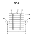
- alignment marks are utilized as shown in FIG. 1 . Alignment marks are formed on a wafer or workpiece subject to printing as shown in FIG. 2 . Specifically, FIG. 2 illustrates an exemplary solar cell having two alignment marks. Disposed on a semiconductor substrate 11 are finger electrodes 12, bus bar electrodes 13, and alignment marks 14. First, the shape and location of initial alignment marks (A0, B0 in FIG. 1a ) are previously stored in an image processing device. Secondly, alignment marks (A1, B1 in FIG.
- JP-A 2006-080415 addresses the problem in that alignment marks formed by screen printing are image processed for positional correction and checked for any anomaly at the same time. When an anomaly is detected, the process is interrupted.
- the method of JP-A 2006-080415 does not address changes of alignment marks with time (e.g., oozing due to lowering of paste viscosity, incidental flaws). Since the process is interrupted whenever an anomaly is detected in the mark, the down time is a problem.
- Citation List Patent Document 1 JP-A 2006-080415
- An object of the invention is to provide a screen printing method capable of multilayer printing at a high accuracy while facilitating registration.
- the present invention provides a screen printing method defined below.
- the screen printing method of the invention ensures the accuracy and ease of multilayer screen printing.
- the method uses a system comprising a camera for producing image data, and an image processing device for storing image data and for delivering reference data for printing; a first layer and an alignment mark are printed on a workpiece, the alignment mark is then imaged by the camera to produce image data, the alignment mark image data is stored in the image processing device where the reference data is renewed with the image data, and second and subsequent layers are printed using the renewed reference data.
- a workpiece having a plurality of layers printed is formed by screen printing a first layer and an alignment mark on a workpiece, then screen printing second and subsequent layers.
- the workpiece is positioned such that the alignment mark actually printed on the workpiece may coincide with the alignment mark previously stored in an image processing device as the reference image, after which the steps of screen printing second and subsequent layers are carried out.
- the invention intends to improve the accuracy of a plurality of screen printing steps. According to the invention, after a first layer and an alignment mark are printed on a workpiece, the alignment mark is imaged by a camera so that the alignment mark is stored as image data in an image processing device adapted to deliver reference data for subsequent printing, and the alignment mark image data is used to renew the reference data in the image processing device.
- the invention is advantageous when electrodes of solar cells are formed by the screen printing process.
- a first layer of electrode and an alignment mark are printed on a substrate.
- the alignment mark is imaged by a camera so that the alignment mark is stored as (a set of) image data in an image processing device.
- the image data is used to renew the reference data in the image processing device, which deliver the renewed reference data for subsequent printing.
- positional adjustment of the printer stage and multilayer electrode formation can be performed independent of any change with time of alignment marks actually printed. In this way, the invention overcomes any change with time or anomaly of alignment mark.
- FIG. 2 shows the light-receiving surface of a solar cell having alignment marks 14 and 14.
- FIG. 1 is an enlarged view of two alignment marks on the solar cell.
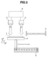
- FIG. 3 schematically illustrates a screen printing system for forming multilayer electrodes on the solar cell. Illustrated in FIG. 3 are a workpiece 1, a movable stage 2 which are movable in X, Y and ⁇ , stationary cameras 3 disposed above the stage 2 for recognizing alignment marks printed on the workpiece 1, a fixed screen 4, a ball screw 5 for moving the stage 2 to immediately below the screen 4, and an image processing device 6.
- FIG. 3 schematically illustrates a screen printing system for forming multilayer electrodes on the solar cell. Illustrated in FIG. 3 are a workpiece 1, a movable stage 2 which are movable in X, Y and ⁇ , stationary cameras 3 disposed above the stage 2 for recognizing alignment marks printed on the workpiece 1, a fixed screen 4, a ball screw 5 for moving the stage 2 to immediately below the screen 4, and an
- the position (X, Y, ⁇ ) of the stage is finely adjusted so that alignment marks A1, B1 in FIG. 1b actually printed as an identical pattern on the workpiece 1 at the same time as the first layer of electrode may overlap the initial alignment marks A0, B0 within a certain tolerance. After the completion of fine adjustment, second and subsequent layers of electrode paste are printed.
- alignment marks A0, B0 stored beforehand in the image processing device as the reference image and alignment marks A1, B1 actually printed in an identical pattern on the workpiece at the same time as the first layer of electrode are approximate in shape, high accuracy printing is possible.
- some changes occur, for example, the electrode paste changes its viscosity, some openings of the screen are clogged, or the workpiece is fissured.
- the shape of alignment marks A1, B1 is changed, resulting in alignment marks A2, B2 as shown in FIG. 1c .
- the difference in shape between alignment marks A0, B0 and alignment marks A2, B2 is too large, inhibiting accurate adjustment of the stage position. This reduces the position accuracy of printing second and subsequent layers of electrode.
- the following mechanism addresses the inaccurate positioning.
- the substrate is moved past an appearance anomaly inspection apparatus prior to printing of second and subsequent layers of electrode pattern.
- the inspection apparatus the first layer of electrode is inspected for thickening, disconnection, contamination or the like.
- the alignment mark actually printed on the workpiece is imaged by a camera, and the resultant shape data is stored in the image processing device.
- the shape data is sequentially overwritten for use as alignment marks A0, B0, thereby reducing the difference in shape between alignment marks A0, B0 previously stored as the reference image in the image processing device and alignment marks A1, B1 actually printed on the workpiece in the identical pattern at the same time as the first layer.
- the position accuracy is maintained during a long period of multilayer electrode printing.
- the workpiece and alignment marks are given ID number.
- the alignment marks are read out and image processed.
- a time of about 0.05 to 0.10 second is necessary for the processing.
- the frequency of renewal is once every layer, takt time increases. Accordingly a compromise may be found between manufacturing yield and cycle time if the frequency of overwriting alignment marks in the image processing device is every 5,000 layers or less. Namely, alignment marks are renewed in the image processing device every 1 to 5,000 printing steps, more preferably every 1 to 3,000 printing steps, and even more preferably every 1 to 1,000 printing steps.
- a higher accuracy is expected when the number of alignment marks is two or more.
- the shape of alignment marks may be T shape as shown in FIG. 1 , or any of other various shapes including crisscross, rectangular, triangular, elliptic and semi-circular shapes.
- the invention is applicable independent of the shape of alignment marks.
- the alignment mark is of such shape that a ratio of the total length of sides of a rectangle that circumscribes the outermost periphery of the alignment mark to the total length of outer sides of the alignment mark itself is from 1:0.1 to 1:50, more preferably 1:0.5 to 1:20, most preferably 1:0.6 to 1:10, especially 1:0.8 or 1.1.
- the alignment mark is of a shape identifiable by image processing, but sensitive to a change in the course of plural printing steps.
- the alignment mark is used to renew the reference data in the image processing device.
- the alignment mark is a regular triangle having three sides with length "a”
- a rectangle having four sides with lengths "a” and ⁇ 3a/2 circumscribes the triangle.
- a ratio of the total length of sides of a rectangle that circumscribes the outermost periphery of the alignment mark to the total length of outer sides of the alignment mark itself is (2+ ⁇ 3)a : 3a ⁇ 1:0.80.
- the method of the invention is advantageously employed, in the manufacture of a solar cell, when finger electrodes and/or bus bar electrodes are formed as two or multiple layers by the screen printing technique as shown in FIG. 2 .
- the workpiece is a wafer of a solar cell on which an electrode pattern is printed as the first layer. While the alignment mark printed at the same time as the first layer is used as a registration reference on the side of the workpiece, and the alignment mark printed at the same time as the first layer or any alignment mark printed within 5,000 printing steps at maximum is used as a registration reference on the side of the image processing device, at least one more layer of electrode pattern is printed to form an electrode of multilayer structure.
- the solar cell has the first layer of finger electrode pattern, and the alignment mark is formed utilizing a part of the first layer of finger electrode pattern. Then the alignment mark may be formed without increasing the shadow loss.
- a part of printed pattern is utilized as the alignment mark so that no partition is defined between the alignment mark and the printed pattern. Data for all the region viewed by the camera may be fed as the alignment mark image data to the image processing device.
- finger electrodes are formed by multilayer screen printing in accordance with the method described in conjunction with FIGS. 1 to 3 .
- the shape data is stored and overwritten for renewal in the image processing device every 1,000 layers of printing.
- Comparative Example such renewal was omitted.
- Table 1 tabulates the percent occurrence of appearance anomaly owing to any shift between the first layer and the second or subsequent layer. Comparison is made after about 30,000 layers are printed.
- the term "appearance anomaly" indicates that the width of electrode fingers becomes equal to or more than 150 ⁇ m. The time required for printing does not differ substantially between Example and Comparative Example.
- Table 1 Occurrence of appearance anomaly (%) Example 0.40 Comparative Example 10.34
- the screen printing method of Comparative Example is orthodox. As seen from Table 1, the screen printing method of the invention ensures accurate printing with minimized occurrence of appearance anomaly as compared with the orthodox method.
Landscapes
- Engineering & Computer Science (AREA)
- Mechanical Engineering (AREA)
- Manufacturing & Machinery (AREA)
- Microelectronics & Electronic Packaging (AREA)
- Screen Printers (AREA)
- Photovoltaic Devices (AREA)
- Printing Methods (AREA)
- Inking, Control Or Cleaning Of Printing Machines (AREA)
Abstract
Description
- This invention relates to a screen printing method, and more particularly, to a screen printing method employing an alignment mode for registration of printed patterns.
- Solar cells are desired to have electrodes with a high aspect ratio. The desired electrode may be formed by screen printing an electrode paste to form a first electrode layer, and repeating screen printing to lay plural electrode layers thereon. This method is known as multilayer electrode printing. To carry out accurate multilayer electrode printing, alignment marks are utilized as shown in
FIG. 1 . Alignment marks are formed on a wafer or workpiece subject to printing as shown inFIG. 2 . Specifically,FIG. 2 illustrates an exemplary solar cell having two alignment marks. Disposed on asemiconductor substrate 11 arefinger electrodes 12,bus bar electrodes 13, andalignment marks 14. First, the shape and location of initial alignment marks (A0, B0 inFIG. 1a ) are previously stored in an image processing device. Secondly, alignment marks (A1, B1 inFIG. 1b ) of the same shape as the initial alignment marks are printed on the substrate at the same time as is a first layer of electrode. Thirdly, the workpiece having marks A1, B1 printed is placed on a stage for printing second and subsequent layers of electrode. Fourthly, marks A1, B1 are recognized by cameras, and the stage position is finely adjusted so that marks A1, B1 may overlay the positional data of marks A0, B0 of the same shape. Thereafter, electrode paste is printed. In this way, a multilayer electrode can be formed. - While printing is repeated, there can occur changes in viscosity of the electrode paste or fissure of the workpiece, whereupon accurate alignment marks are no longer printed. There result alignment marks A2 and B2 in
FIG. 1c . Now that the difference in shape between the mark actually printed and the mark previously stored in the image processing device is of significance, accurate image processing becomes impossible. As a result, the lower layer of electrode and the overlying layer of electrode printed thereon are shifted to increase a shadow loss, detracting from the conversion of the solar cell. -
JP-A 2006-080415 JP-A 2006-080415
Citation List
Patent Document 1:JP-A 2006-080415 - In an example wherein multilayer electrodes in solar cells are formed, as the difference in shape between a mark stored in an image processing device and a mark actually printed becomes of significance, accurate image processing becomes impossible. As a result, the lower layer of electrode and the overlying layer of electrode printed thereon are shifted to increase a shadow loss, resulting in the solar cell with reduced conversion.
- An object of the invention is to provide a screen printing method capable of multilayer printing at a high accuracy while facilitating registration.
- Accordingly, the present invention provides a screen printing method defined below.
- [1] A method for improving accuracy during a plurality of screen printing steps, wherein after a first layer to be printed and an alignment mark are printed on a workpiece,
the alignment mark is imaged by a camera so that the alignment mark is stored as image data in an image processing device adapted to deliver reference data for subsequent printing, and
the image data is used to renew the reference data in the image processing device. - [2] The screen printing method of [1] wherein the alignment mark is of such shape that a ratio of the total length of sides of a rectangle that circumscribes the outermost periphery of the alignment mark to the total length of outer sides of the alignment mark itself is from 1:0.1 to 1:50.
- [3] The screen printing method of [1] or [2] wherein the alignment mark is of T, crisscross, rectangular, triangular, elliptic or semi-circular shape.
- [4] The screen printing method of any one of [1] to [3] wherein at least two alignment marks are printed on the workpiece and used for image processing.
- [5] The screen printing method of any one of [1] to [4] wherein the frequency of renewing the reference data with the alignment mark image data is every 1 to 5,000 printing steps.
- [6] The screen printing method of any one of [1] to [5] wherein the layer printed constitutes an electrode of a solar cell.
- [7] The screen printing method of [6] wherein
the workpiece is a wafer of a solar cell on which an electrode pattern is printed as the first layer, and
at least one more layer of electrode pattern is printed to form an electrode of multilayer structure while the alignment mark printed at the same time as the first layer is used as a registration reference on the side of the workpiece, and the alignment mark printed at the same time as the first layer or any alignment mark printed within 5,000 printing steps at maximum is used as a registration reference on the side of the image processing device. - [8] The screen printing method of [6] or [7] wherein the solar cell has the first layer of finger electrode pattern, and the alignment mark is formed utilizing a part of the first layer of finger electrode pattern.
- [9] The screen printing method of any one of [1] to [8] wherein a part of printed pattern is utilized as the alignment mark so that no partition is defined between the alignment mark and the printed pattern, and all the region viewed by the camera is fed as the alignment mark image data to the image processing device.
- The screen printing method of the invention ensures the accuracy and ease of multilayer screen printing.
-
-
FIG. 1 illustrates different examples of alignment marks,FIG. 1a showing alignment marks previously stored as the reference image in an image processing device,FIG. 1b showing alignment marks actually printed, andFIG. 1c showing alignment marks which are deformed as a result of repeated printing. -
FIG. 2 is a plan view of a solar cell substrate on which electrodes and alignment marks are printed. -
FIG. 3 schematically illustrates a screen printing system. - In the method for improving accuracy during a plurality of screen printing steps according to the present invention; the method uses a system comprising a camera for producing image data, and an image processing device for storing image data and for delivering reference data for printing; a first layer and an alignment mark are printed on a workpiece, the alignment mark is then imaged by the camera to produce image data, the alignment mark image data is stored in the image processing device where the reference data is renewed with the image data, and second and subsequent layers are printed using the renewed reference data. A workpiece having a plurality of layers printed is formed by screen printing a first layer and an alignment mark on a workpiece, then screen printing second and subsequent layers. The workpiece is positioned such that the alignment mark actually printed on the workpiece may coincide with the alignment mark previously stored in an image processing device as the reference image, after which the steps of screen printing second and subsequent layers are carried out. The invention intends to improve the accuracy of a plurality of screen printing steps. According to the invention, after a first layer and an alignment mark are printed on a workpiece, the alignment mark is imaged by a camera so that the alignment mark is stored as image data in an image processing device adapted to deliver reference data for subsequent printing, and the alignment mark image data is used to renew the reference data in the image processing device.
- The invention is advantageous when electrodes of solar cells are formed by the screen printing process. A first layer of electrode and an alignment mark are printed on a substrate. When the substrate goes past an appearance inspection apparatus, the alignment mark is imaged by a camera so that the alignment mark is stored as (a set of) image data in an image processing device. The image data is used to renew the reference data in the image processing device, which deliver the renewed reference data for subsequent printing. Then, positional adjustment of the printer stage and multilayer electrode formation can be performed independent of any change with time of alignment marks actually printed. In this way, the invention overcomes any change with time or anomaly of alignment mark.
- Referring to the drawings, one embodiment of the alignment method according to the invention is described.
FIG. 2 shows the light-receiving surface of a solar cell having alignment marks 14 and 14.FIG. 1 is an enlarged view of two alignment marks on the solar cell.FIG. 3 schematically illustrates a screen printing system for forming multilayer electrodes on the solar cell. Illustrated inFIG. 3 are a workpiece 1, amovable stage 2 which are movable in X, Y and θ,stationary cameras 3 disposed above thestage 2 for recognizing alignment marks printed on the workpiece 1, a fixedscreen 4, aball screw 5 for moving thestage 2 to immediately below thescreen 4, and animage processing device 6. Beforehand, the shape and position data of alignment marks A0, B0 inFIG. 1a is stored in theimage processing device 6 as the reference image. The position (X, Y, θ) of the stage is finely adjusted so that alignment marks A1, B1 inFIG. 1b actually printed as an identical pattern on the workpiece 1 at the same time as the first layer of electrode may overlap the initial alignment marks A0, B0 within a certain tolerance. After the completion of fine adjustment, second and subsequent layers of electrode paste are printed. - If alignment marks A0, B0 stored beforehand in the image processing device as the reference image and alignment marks A1, B1 actually printed in an identical pattern on the workpiece at the same time as the first layer of electrode are approximate in shape, high accuracy printing is possible. However, as printing operation is repeated, some changes occur, for example, the electrode paste changes its viscosity, some openings of the screen are clogged, or the workpiece is fissured. Then the shape of alignment marks A1, B1 is changed, resulting in alignment marks A2, B2 as shown in
FIG. 1c . As such, the difference in shape between alignment marks A0, B0 and alignment marks A2, B2 is too large, inhibiting accurate adjustment of the stage position. This reduces the position accuracy of printing second and subsequent layers of electrode. The following mechanism addresses the inaccurate positioning. - After a first layer of electrode pattern and an alignment mark are printed on a substrate, the substrate is moved past an appearance anomaly inspection apparatus prior to printing of second and subsequent layers of electrode pattern. In the inspection apparatus, the first layer of electrode is inspected for thickening, disconnection, contamination or the like. At the same time as appearance anomaly inspection, the alignment mark actually printed on the workpiece is imaged by a camera, and the resultant shape data is stored in the image processing device. The shape data is sequentially overwritten for use as alignment marks A0, B0, thereby reducing the difference in shape between alignment marks A0, B0 previously stored as the reference image in the image processing device and alignment marks A1, B1 actually printed on the workpiece in the identical pattern at the same time as the first layer. As a result, the position accuracy is maintained during a long period of multilayer electrode printing.
- Ideally, when the first layer and alignment marks are printed on the workpiece, the workpiece and alignment marks are given ID number. When the workpiece with the relevant ID number is subjected to second printing, the alignment marks are read out and image processed. However, when the alignment marks are overwritten, a time of about 0.05 to 0.10 second is necessary for the processing. Thus, if the frequency of renewal is once every layer, takt time increases. Accordingly a compromise may be found between manufacturing yield and cycle time if the frequency of overwriting alignment marks in the image processing device is every 5,000 layers or less. Namely, alignment marks are renewed in the image processing device every 1 to 5,000 printing steps, more preferably every 1 to 3,000 printing steps, and even more preferably every 1 to 1,000 printing steps.
- A higher accuracy is expected when the number of alignment marks is two or more.
- The shape of alignment marks may be T shape as shown in
FIG. 1 , or any of other various shapes including crisscross, rectangular, triangular, elliptic and semi-circular shapes. The invention is applicable independent of the shape of alignment marks. - Also preferably, the alignment mark is of such shape that a ratio of the total length of sides of a rectangle that circumscribes the outermost periphery of the alignment mark to the total length of outer sides of the alignment mark itself is from 1:0.1 to 1:50, more preferably 1:0.5 to 1:20, most preferably 1:0.6 to 1:10, especially 1:0.8 or 1.1. To increase the registration accuracy based on alignment, the alignment mark is of a shape identifiable by image processing, but sensitive to a change in the course of plural printing steps. As a countermeasure for the accuracy of registration based on alignment and a shape change of alignment mark in the course of plural printing steps, the alignment mark is used to renew the reference data in the image processing device.
- In one example where the alignment mark is a regular triangle having three sides with length "a", a rectangle having four sides with lengths "a" and √3a/2 circumscribes the triangle. In this example, a ratio of the total length of sides of a rectangle that circumscribes the outermost periphery of the alignment mark to the total length of outer sides of the alignment mark itself is (2+√3)a : 3a ≒ 1:0.80.
- The method of the invention is advantageously employed, in the manufacture of a solar cell, when finger electrodes and/or bus bar electrodes are formed as two or multiple layers by the screen printing technique as shown in
FIG. 2 . - Specifically, the workpiece is a wafer of a solar cell on which an electrode pattern is printed as the first layer. While the alignment mark printed at the same time as the first layer is used as a registration reference on the side of the workpiece, and the alignment mark printed at the same time as the first layer or any alignment mark printed within 5,000 printing steps at maximum is used as a registration reference on the side of the image processing device, at least one more layer of electrode pattern is printed to form an electrode of multilayer structure. In a preferred embodiment, the solar cell has the first layer of finger electrode pattern, and the alignment mark is formed utilizing a part of the first layer of finger electrode pattern. Then the alignment mark may be formed without increasing the shadow loss. In a further preferred embodiment, a part of printed pattern is utilized as the alignment mark so that no partition is defined between the alignment mark and the printed pattern. Data for all the region viewed by the camera may be fed as the alignment mark image data to the image processing device.
- In the manufacture of a solar cell, finger electrodes are formed by multilayer screen printing in accordance with the method described in conjunction with
FIGS. 1 to 3 . In Example, the shape data is stored and overwritten for renewal in the image processing device every 1,000 layers of printing. In Comparative Example, such renewal was omitted. Table 1 tabulates the percent occurrence of appearance anomaly owing to any shift between the first layer and the second or subsequent layer. Comparison is made after about 30,000 layers are printed. The term "appearance anomaly" indicates that the width of electrode fingers becomes equal to or more than 150 µm. The time required for printing does not differ substantially between Example and Comparative Example.Table 1 Occurrence of appearance anomaly (%) Example 0.40 Comparative Example 10.34 - The screen printing method of Comparative Example is orthodox. As seen from Table 1, the screen printing method of the invention ensures accurate printing with minimized occurrence of appearance anomaly as compared with the orthodox method.
- In respect of numerical ranges disclosed in the present description it will of course be understood that in the normal way the technical criterion for the upper limit is different from the technical criterion for the lower limit, i.e. the upper and lower limits are intrinsically distinct proposals.
Claims (9)
- A screen printing method which applies a plurality of screen printing steps to a workpiece to form plural layers thereon, wherein after a first layer and an alignment mark are printed on a workpiece, an image processing device compares the printed alignment mark with stored alignment mark reference data to register the workpiece position for subsequent printing,
characterised in that
the printed alignment mark is imaged by a camera and is stored as image data in an image processing device which delivers reference data for registering subsequent printing, and
the printed alignment mark image data are used to renew stored alignment mark reference data in the image processing device. - The screen printing method of claim 1 wherein the alignment mark is of such shape that a ratio of the total length of sides of a rectangle that circumscribes the outermost periphery of the alignment mark to the total length of outer sides of the alignment mark itself is from 1:0.1 to 1:50.
- The screen printing method of claim 1 or 2 wherein the alignment mark is of T, crisscross, rectangular, triangular, elliptic or semi-circular shape.
- The screen printing method of any one of claims 1 to 3 wherein at least two alignment marks are printed on the workpiece and used for image processing.
- The screen printing method of any one of claims 1 to 4 wherein the frequency of renewing the reference data with the alignment mark image data is every 1 to 5,000 printing steps.
- The screen printing method of any one of claims 1 to 5 wherein the layer printed constitutes an electrode of a solar cell.
- The screen printing method of claim 6 wherein
the workpiece is a wafer of a solar cell on which an electrode pattern is printed as the first layer, and
at least one more layer of electrode pattern is printed to form an electrode of multilayer structure while the alignment mark printed at the same time as the first layer is used as a registration reference on the side of the workpiece, and the alignment mark printed at the same time as the first layer or any alignment mark printed within 5,000 printing steps at maximum is used as a registration reference on the side of the image processing device. - The screen printing method of claim 6 or 7 wherein the solar cell has the first layer of finger electrode pattern, and the alignment mark is formed utilizing a part of the first layer of finger electrode pattern.
- The screen printing method of any one of claims 1 to 8 wherein a part of printed pattern is utilized as the alignment mark so that no partition is defined between the alignment mark and the printed pattern, and all the region viewed by the camera is fed as the alignment mark image data to the image processing device.
Applications Claiming Priority (1)
| Application Number | Priority Date | Filing Date | Title |
|---|---|---|---|
| JP2009028072 | 2009-02-10 |
Publications (2)
| Publication Number | Publication Date |
|---|---|
| EP2216175A1 true EP2216175A1 (en) | 2010-08-11 |
| EP2216175B1 EP2216175B1 (en) | 2012-11-14 |
Family
ID=42115858
Family Applications (1)
| Application Number | Title | Priority Date | Filing Date |
|---|---|---|---|
| EP10250225A Active EP2216175B1 (en) | 2009-02-10 | 2010-02-10 | Screen printing method |
Country Status (5)
| Country | Link |
|---|---|
| US (1) | US8783174B2 (en) |
| EP (1) | EP2216175B1 (en) |
| JP (1) | JP5488015B2 (en) |
| CN (1) | CN101800265B (en) |
| TW (1) | TWI503233B (en) |
Cited By (2)
| Publication number | Priority date | Publication date | Assignee | Title |
|---|---|---|---|---|
| WO2012103188A3 (en) * | 2011-01-25 | 2013-03-07 | E. I. Du Pont De Nemours And Company | A method for calculating an offset value for aligned deposition of a second pattern onto a first pattern |
| ITUD20120149A1 (en) * | 2012-08-31 | 2014-03-01 | Applied Materials Italia Srl | METHOD AND PRINTING SYSTEM OF A SCHEME ON A SUBSTRATE |
Families Citing this family (22)
| Publication number | Priority date | Publication date | Assignee | Title |
|---|---|---|---|---|
| KR101176133B1 (en) | 2010-12-24 | 2012-08-22 | 엘지전자 주식회사 | Screen mask, solar cell and solar cell manufacturing method including alignment mark |
| CN102179996B (en) * | 2011-01-14 | 2012-06-27 | 浙江大学 | Substrate positioning method suitable for screen printing technology |
| JP5675476B2 (en) * | 2011-04-18 | 2015-02-25 | 株式会社カネカ | Crystalline silicon solar cell |
| ITUD20110135A1 (en) * | 2011-08-25 | 2013-02-26 | Applied Materials Italia Srl | METHOD AND CONTROL SYSTEM FOR THE PRINTING OF A MULTILAYER SCHEME |
| JP5804558B2 (en) * | 2011-10-15 | 2015-11-04 | 株式会社セリアエンジニアリング | Manufacturing method of solar cell |
| CN103171254B (en) * | 2011-12-23 | 2016-04-27 | 昆山允升吉光电科技有限公司 | A kind of solar battery sheet positive electrode screen plate |
| JP5988107B2 (en) * | 2012-02-03 | 2016-09-07 | パナソニックIpマネジメント株式会社 | Manufacturing method of semiconductor device using screen printing apparatus |
| CN102779861B (en) * | 2012-07-31 | 2014-12-31 | 宁波尤利卡太阳能科技发展有限公司 | Electrode structure with grid lines on front surface |
| JP5907110B2 (en) * | 2013-04-12 | 2016-04-20 | 信越化学工業株式会社 | Screen printing method and screen printing apparatus |
| WO2014171890A1 (en) * | 2013-04-15 | 2014-10-23 | Heptagon Micro Optics Pte. Ltd. | Accurate positioning and alignment of a component during processes such as reflow soldering |
| US9126398B2 (en) * | 2013-07-26 | 2015-09-08 | Asm Assembly Systems Singapore Pte Ltd | Apparatus for paste material printing, and printing method |
| KR102053138B1 (en) | 2013-09-27 | 2019-12-06 | 엘지전자 주식회사 | Solar cell |
| WO2015068248A1 (en) * | 2013-11-07 | 2015-05-14 | 三菱電機株式会社 | Solar cell, manufacturing method therefor, and solar-cell module |
| CN105684158B (en) * | 2013-11-07 | 2017-06-23 | 三菱电机株式会社 | Solar cell and its manufacture method, solar module |
| CN103839861B (en) * | 2014-03-18 | 2016-11-16 | 常州天合光能有限公司 | Multiple overprint alignment method for fine grids on the surface of solar cells |
| CN104129183B (en) * | 2014-08-06 | 2016-08-17 | 中利腾晖光伏科技有限公司 | A kind of printing process of solar battery sheet front electrode |
| WO2017026016A1 (en) * | 2015-08-07 | 2017-02-16 | 三菱電機株式会社 | Solar battery cell and method for fabricating solar battery cell |
| CN108263074A (en) * | 2017-12-29 | 2018-07-10 | 广州泰行智能科技有限公司 | Localization method, device, terminal device and the readable storage medium storing program for executing of silk-screen halftone |
| CN109004067A (en) * | 2018-09-26 | 2018-12-14 | 浙江晶科能源有限公司 | A kind of preparation method of n-type solar cell |
| CN110491955A (en) * | 2018-09-30 | 2019-11-22 | 协鑫集成科技股份有限公司 | Solar battery and preparation method thereof |
| CN111668339A (en) * | 2020-04-23 | 2020-09-15 | 天津爱旭太阳能科技有限公司 | A kind of solar cell front electrode alignment printing method and preparation method |
| CN113103743A (en) * | 2021-03-24 | 2021-07-13 | 天合光能股份有限公司 | Screen printing plate design and printing method for screen printing of sliced solar cells |
Citations (4)
| Publication number | Priority date | Publication date | Assignee | Title |
|---|---|---|---|---|
| US5176078A (en) * | 1991-05-27 | 1993-01-05 | Hitachi Techno Engineering Co., Ltd. | Screen printing machine |
| JPH08192337A (en) * | 1995-01-10 | 1996-07-30 | Hitachi Ltd | Alignment method |
| DE102004048680A1 (en) * | 2003-10-08 | 2005-05-19 | Sharp K.K. | Manufacturing solar cell involves making grid electrode with narrow width on light reception surface of substrate with pn junction by sintering metal paste material, making rod-shaped main electrode electrically connected to grid electrode |
| JP2006080415A (en) | 2004-09-13 | 2006-03-23 | Murata Mfg Co Ltd | Manufacturing method of multilayer ceramic electronic component |
Family Cites Families (16)
| Publication number | Priority date | Publication date | Assignee | Title |
|---|---|---|---|---|
| EP0126723A3 (en) * | 1983-05-18 | 1986-10-29 | Svecia Silkscreen Maskiner AB | Method and arrangement for positioning a second pattern origination from a pattern formed on a stencil in relation to a material intended for the pattern |
| SE8405067L (en) * | 1984-10-10 | 1986-04-11 | Svecia Silkscreen Maskiner Ab | DEVICE FOR INSTALLING IN A STONE PRINTING MACHINE FROM A PRINCIPAL OF A STONE CILATED SAMPLES CONCERNING OTHER MONSTERS IN CONDITIONS TO A STANDARD PROPOSED MATERIAL |
| JP3059473B2 (en) * | 1990-10-01 | 2000-07-04 | 大日本印刷株式会社 | Fine pattern transfer method and fine pattern transfer device |
| JPH09226224A (en) * | 1996-02-20 | 1997-09-02 | Canon Inc | Pattern printing method, printing apparatus, thick film circuit board using the printing method, and image forming apparatus using the thick film circuit board |
| JPH11986A (en) * | 1997-06-13 | 1999-01-06 | Pioneer Electron Corp | Method for screen printing |
| JP2000246880A (en) * | 1999-02-25 | 2000-09-12 | Canon Inc | Reference mark of printing plate and alignment method using the same |
| JP2003037277A (en) * | 2001-05-15 | 2003-02-07 | Canon Inc | Photovoltaic element and method of manufacturing photovoltaic element |
| JP4403306B2 (en) * | 2002-10-07 | 2010-01-27 | Dic株式会社 | How to prevent blanket piling in a printing press |
| JP2006187912A (en) * | 2005-01-05 | 2006-07-20 | Denso Corp | Screen printing method and apparatus |
| JP4944407B2 (en) * | 2005-08-01 | 2012-05-30 | 富士機械製造株式会社 | Screen / substrate alignment method and apparatus |
| JP4899400B2 (en) * | 2005-09-30 | 2012-03-21 | 株式会社日立プラントテクノロジー | Screen printing device |
| JP4324805B2 (en) * | 2006-01-26 | 2009-09-02 | 智雄 松下 | Pattern forming device |
| JP4964522B2 (en) * | 2006-07-12 | 2012-07-04 | ヤマハ発動機株式会社 | Screen printing device |
| JP5018368B2 (en) * | 2006-09-25 | 2012-09-05 | 凸版印刷株式会社 | Printing method |
| JP2008179029A (en) * | 2007-01-24 | 2008-08-07 | Matsushita Electric Ind Co Ltd | Screen printing apparatus and screen printing method |
| FR2914501B1 (en) * | 2007-03-28 | 2009-12-04 | Commissariat Energie Atomique | PHOTOVOLTAIC DEVICE WITH DISCONTINUOUS INTERDIGITED HETEROJUNCTION STRUCTURE |
-
2010
- 2010-02-08 JP JP2010025047A patent/JP5488015B2/en active Active
- 2010-02-09 US US12/702,695 patent/US8783174B2/en active Active
- 2010-02-09 TW TW099103968A patent/TWI503233B/en active
- 2010-02-10 CN CN201010116537.6A patent/CN101800265B/en active Active
- 2010-02-10 EP EP10250225A patent/EP2216175B1/en active Active
Patent Citations (4)
| Publication number | Priority date | Publication date | Assignee | Title |
|---|---|---|---|---|
| US5176078A (en) * | 1991-05-27 | 1993-01-05 | Hitachi Techno Engineering Co., Ltd. | Screen printing machine |
| JPH08192337A (en) * | 1995-01-10 | 1996-07-30 | Hitachi Ltd | Alignment method |
| DE102004048680A1 (en) * | 2003-10-08 | 2005-05-19 | Sharp K.K. | Manufacturing solar cell involves making grid electrode with narrow width on light reception surface of substrate with pn junction by sintering metal paste material, making rod-shaped main electrode electrically connected to grid electrode |
| JP2006080415A (en) | 2004-09-13 | 2006-03-23 | Murata Mfg Co Ltd | Manufacturing method of multilayer ceramic electronic component |
Cited By (7)
| Publication number | Priority date | Publication date | Assignee | Title |
|---|---|---|---|---|
| WO2012103188A3 (en) * | 2011-01-25 | 2013-03-07 | E. I. Du Pont De Nemours And Company | A method for calculating an offset value for aligned deposition of a second pattern onto a first pattern |
| US8673793B2 (en) | 2011-01-25 | 2014-03-18 | Innovalight Inc | Method for automatic offset calculation for deposition of an aligned metal pattern onto selective emitter pattern and subsequent monitoring of alignment |
| ITUD20120149A1 (en) * | 2012-08-31 | 2014-03-01 | Applied Materials Italia Srl | METHOD AND PRINTING SYSTEM OF A SCHEME ON A SUBSTRATE |
| EP2704204A1 (en) * | 2012-08-31 | 2014-03-05 | Applied Materials Italia S.R.L. | Method and apparatus for printing a pattern on a substrate |
| CN103660551A (en) * | 2012-08-31 | 2014-03-26 | 应用材料意大利有限公司 | Method and apparatus for printing a pattern on a substrate |
| CN106985515A (en) * | 2012-08-31 | 2017-07-28 | 应用材料意大利有限公司 | The method and apparatus of printed patterns on substrate |
| CN106985515B (en) * | 2012-08-31 | 2019-05-28 | 应用材料意大利有限公司 | The method and apparatus of printed patterns on substrate |
Also Published As
| Publication number | Publication date |
|---|---|
| TW201043472A (en) | 2010-12-16 |
| US8783174B2 (en) | 2014-07-22 |
| JP2010208317A (en) | 2010-09-24 |
| TWI503233B (en) | 2015-10-11 |
| EP2216175B1 (en) | 2012-11-14 |
| JP5488015B2 (en) | 2014-05-14 |
| US20100229740A1 (en) | 2010-09-16 |
| CN101800265B (en) | 2014-04-02 |
| CN101800265A (en) | 2010-08-11 |
Similar Documents
| Publication | Publication Date | Title |
|---|---|---|
| EP2216175B1 (en) | Screen printing method | |
| KR101058160B1 (en) | Solder Print Inspection Device and Component Mounting System | |
| US6850855B2 (en) | Apparatus and method for inspecting working operations on circuit substrate, and system and method for fabricating electric circuit | |
| KR102156690B1 (en) | Electronic component mounting device and mounting method, and method for manufacturing package component | |
| JP5599411B2 (en) | Automatic screen printing process | |
| US8807026B2 (en) | Method for printing a conductor in two superimposed layers by screen-printing | |
| EP3405972B1 (en) | Inkjet printing system and method for processing substrates | |
| TW201838724A (en) | Droplet ejecting apparatus, droplet ejecting method, and computer storage medium | |
| CN112631080B (en) | Exposure method of double-workbench exposure machine | |
| KR101175871B1 (en) | Method for revision of printing error in pcb | |
| CN104078404A (en) | Manufacturing apparatus of electronic component and manufacturing method thereof | |
| JP4871234B2 (en) | Abnormality detection method and apparatus for component mounting apparatus | |
| JP7106608B2 (en) | Mark detection device, alignment device, film formation device, mark detection method, and film formation method | |
| JP2006108200A (en) | Solder printing system | |
| JP2008198730A (en) | Surface mounting machine, screen printing device and mounting line | |
| US20120272510A1 (en) | Mounting system, electronic component mounting method, substrate production method, and program | |
| EP4120023A1 (en) | Pattern transfer sheet, method of monitoring pattern transfer printing, and pattern transfer printing system | |
| KR102089097B1 (en) | Semiconductor package arrange apparatus, manufacturing apparatus, arrange method of semiconductor package and manufacturing method of electronic part | |
| CN112331582B (en) | Chip mounting device and method of manufacturing semiconductor device | |
| JP5577770B2 (en) | Coordinate correction method | |
| WO2017056538A1 (en) | Printing apparatus and printing method | |
| JP4774890B2 (en) | Ink ejection printing device | |
| JP2013084646A (en) | Substrate processing system, substrate supply order determination method, program and storage medium | |
| Gautero et al. | Functional inkjet printing equipment: A set of features leading to productive results | |
| CN120807983B (en) | Steel mesh and PCB size matching dynamic mapping method and device |
Legal Events
| Date | Code | Title | Description |
|---|---|---|---|
| PUAI | Public reference made under article 153(3) epc to a published international application that has entered the european phase |
Free format text: ORIGINAL CODE: 0009012 |
|
| AK | Designated contracting states |
Kind code of ref document: A1 Designated state(s): AT BE BG CH CY CZ DE DK EE ES FI FR GB GR HR HU IE IS IT LI LT LU LV MC MK MT NL NO PL PT RO SE SI SK SM TR |
|
| AX | Request for extension of the european patent |
Extension state: AL BA RS |
|
| 17P | Request for examination filed |
Effective date: 20110204 |
|
| REG | Reference to a national code |
Ref country code: DE Ref legal event code: R079 Ref document number: 602010003616 Country of ref document: DE Free format text: PREVIOUS MAIN CLASS: B41F0033000000 Ipc: B41F0015080000 |
|
| RIC1 | Information provided on ipc code assigned before grant |
Ipc: H01L 31/0224 20060101ALI20120416BHEP Ipc: H05K 3/12 20060101ALI20120416BHEP Ipc: B41M 1/12 20060101ALI20120416BHEP Ipc: B41F 15/26 20060101ALI20120416BHEP Ipc: H01L 31/18 20060101ALI20120416BHEP Ipc: B41F 15/08 20060101AFI20120416BHEP Ipc: B41F 33/00 20060101ALI20120416BHEP |
|
| GRAP | Despatch of communication of intention to grant a patent |
Free format text: ORIGINAL CODE: EPIDOSNIGR1 |
|
| GRAS | Grant fee paid |
Free format text: ORIGINAL CODE: EPIDOSNIGR3 |
|
| GRAA | (expected) grant |
Free format text: ORIGINAL CODE: 0009210 |
|
| RBV | Designated contracting states (corrected) |
Designated state(s): BE DE FR GB |
|
| AK | Designated contracting states |
Kind code of ref document: B1 Designated state(s): BE DE FR GB |
|
| REG | Reference to a national code |
Ref country code: GB Ref legal event code: FG4D |
|
| REG | Reference to a national code |
Ref country code: DE Ref legal event code: R096 Ref document number: 602010003616 Country of ref document: DE Effective date: 20130110 |
|
| PLBE | No opposition filed within time limit |
Free format text: ORIGINAL CODE: 0009261 |
|
| STAA | Information on the status of an ep patent application or granted ep patent |
Free format text: STATUS: NO OPPOSITION FILED WITHIN TIME LIMIT |
|
| 26N | No opposition filed |
Effective date: 20130815 |
|
| REG | Reference to a national code |
Ref country code: DE Ref legal event code: R097 Ref document number: 602010003616 Country of ref document: DE Effective date: 20130815 |
|
| REG | Reference to a national code |
Ref country code: FR Ref legal event code: PLFP Year of fee payment: 7 |
|
| REG | Reference to a national code |
Ref country code: FR Ref legal event code: PLFP Year of fee payment: 8 |
|
| REG | Reference to a national code |
Ref country code: FR Ref legal event code: PLFP Year of fee payment: 9 |
|
| PGFP | Annual fee paid to national office [announced via postgrant information from national office to epo] |
Ref country code: GB Payment date: 20221230 Year of fee payment: 14 |
|
| PGFP | Annual fee paid to national office [announced via postgrant information from national office to epo] |
Ref country code: BE Payment date: 20230117 Year of fee payment: 14 |
|
| P01 | Opt-out of the competence of the unified patent court (upc) registered |
Effective date: 20230512 |
|
| GBPC | Gb: european patent ceased through non-payment of renewal fee |
Effective date: 20240210 |
|
| REG | Reference to a national code |
Ref country code: BE Ref legal event code: MM Effective date: 20240229 |
|
| PG25 | Lapsed in a contracting state [announced via postgrant information from national office to epo] |
Ref country code: BE Free format text: LAPSE BECAUSE OF NON-PAYMENT OF DUE FEES Effective date: 20240229 |
|
| PG25 | Lapsed in a contracting state [announced via postgrant information from national office to epo] |
Ref country code: GB Free format text: LAPSE BECAUSE OF NON-PAYMENT OF DUE FEES Effective date: 20240210 |
|
| PG25 | Lapsed in a contracting state [announced via postgrant information from national office to epo] |
Ref country code: GB Free format text: LAPSE BECAUSE OF NON-PAYMENT OF DUE FEES Effective date: 20240210 Ref country code: BE Free format text: LAPSE BECAUSE OF NON-PAYMENT OF DUE FEES Effective date: 20240229 |
|
| PGFP | Annual fee paid to national office [announced via postgrant information from national office to epo] |
Ref country code: FR Payment date: 20251231 Year of fee payment: 17 |
|
| PGFP | Annual fee paid to national office [announced via postgrant information from national office to epo] |
Ref country code: DE Payment date: 20251230 Year of fee payment: 17 |