EP2214211A2 - Flat panel display apparatus and method of manufacturing the same - Google Patents
Flat panel display apparatus and method of manufacturing the same Download PDFInfo
- Publication number
- EP2214211A2 EP2214211A2 EP10250161A EP10250161A EP2214211A2 EP 2214211 A2 EP2214211 A2 EP 2214211A2 EP 10250161 A EP10250161 A EP 10250161A EP 10250161 A EP10250161 A EP 10250161A EP 2214211 A2 EP2214211 A2 EP 2214211A2
- Authority
- EP
- European Patent Office
- Prior art keywords
- electrode
- layer
- capacitor
- top electrode
- pixel
- Prior art date
- Legal status (The legal status is an assumption and is not a legal conclusion. Google has not performed a legal analysis and makes no representation as to the accuracy of the status listed.)
- Granted
Links
Images





Classifications
-
- G—PHYSICS
- G02—OPTICS
- G02F—OPTICAL DEVICES OR ARRANGEMENTS FOR THE CONTROL OF LIGHT BY MODIFICATION OF THE OPTICAL PROPERTIES OF THE MEDIA OF THE ELEMENTS INVOLVED THEREIN; NON-LINEAR OPTICS; FREQUENCY-CHANGING OF LIGHT; OPTICAL LOGIC ELEMENTS; OPTICAL ANALOGUE/DIGITAL CONVERTERS
- G02F1/00—Devices or arrangements for the control of the intensity, colour, phase, polarisation or direction of light arriving from an independent light source, e.g. switching, gating or modulating; Non-linear optics
- G02F1/01—Devices or arrangements for the control of the intensity, colour, phase, polarisation or direction of light arriving from an independent light source, e.g. switching, gating or modulating; Non-linear optics for the control of the intensity, phase, polarisation or colour
- G02F1/13—Devices or arrangements for the control of the intensity, colour, phase, polarisation or direction of light arriving from an independent light source, e.g. switching, gating or modulating; Non-linear optics for the control of the intensity, phase, polarisation or colour based on liquid crystals, e.g. single liquid crystal display cells
- G02F1/133—Constructional arrangements; Operation of liquid crystal cells; Circuit arrangements
- G02F1/136—Liquid crystal cells structurally associated with a semi-conducting layer or substrate, e.g. cells forming part of an integrated circuit
-
- H—ELECTRICITY
- H10—SEMICONDUCTOR DEVICES; ELECTRIC SOLID-STATE DEVICES NOT OTHERWISE PROVIDED FOR
- H10D—INORGANIC ELECTRIC SEMICONDUCTOR DEVICES
- H10D86/00—Integrated devices formed in or on insulating or conducting substrates, e.g. formed in silicon-on-insulator [SOI] substrates or on stainless steel or glass substrates
- H10D86/40—Integrated devices formed in or on insulating or conducting substrates, e.g. formed in silicon-on-insulator [SOI] substrates or on stainless steel or glass substrates characterised by multiple TFTs
- H10D86/481—Integrated devices formed in or on insulating or conducting substrates, e.g. formed in silicon-on-insulator [SOI] substrates or on stainless steel or glass substrates characterised by multiple TFTs integrated with passive devices, e.g. auxiliary capacitors
-
- G—PHYSICS
- G02—OPTICS
- G02F—OPTICAL DEVICES OR ARRANGEMENTS FOR THE CONTROL OF LIGHT BY MODIFICATION OF THE OPTICAL PROPERTIES OF THE MEDIA OF THE ELEMENTS INVOLVED THEREIN; NON-LINEAR OPTICS; FREQUENCY-CHANGING OF LIGHT; OPTICAL LOGIC ELEMENTS; OPTICAL ANALOGUE/DIGITAL CONVERTERS
- G02F1/00—Devices or arrangements for the control of the intensity, colour, phase, polarisation or direction of light arriving from an independent light source, e.g. switching, gating or modulating; Non-linear optics
- G02F1/01—Devices or arrangements for the control of the intensity, colour, phase, polarisation or direction of light arriving from an independent light source, e.g. switching, gating or modulating; Non-linear optics for the control of the intensity, phase, polarisation or colour
- G02F1/13—Devices or arrangements for the control of the intensity, colour, phase, polarisation or direction of light arriving from an independent light source, e.g. switching, gating or modulating; Non-linear optics for the control of the intensity, phase, polarisation or colour based on liquid crystals, e.g. single liquid crystal display cells
- G02F1/133—Constructional arrangements; Operation of liquid crystal cells; Circuit arrangements
- G02F1/1333—Constructional arrangements; Manufacturing methods
- G02F1/1343—Electrodes
-
- H—ELECTRICITY
- H10—SEMICONDUCTOR DEVICES; ELECTRIC SOLID-STATE DEVICES NOT OTHERWISE PROVIDED FOR
- H10D—INORGANIC ELECTRIC SEMICONDUCTOR DEVICES
- H10D30/00—Field-effect transistors [FET]
- H10D30/60—Insulated-gate field-effect transistors [IGFET]
- H10D30/67—Thin-film transistors [TFT]
- H10D30/6729—Thin-film transistors [TFT] characterised by the electrodes
- H10D30/6737—Thin-film transistors [TFT] characterised by the electrodes characterised by the electrode materials
- H10D30/6739—Conductor-insulator-semiconductor electrodes
-
- H—ELECTRICITY
- H10—SEMICONDUCTOR DEVICES; ELECTRIC SOLID-STATE DEVICES NOT OTHERWISE PROVIDED FOR
- H10D—INORGANIC ELECTRIC SEMICONDUCTOR DEVICES
- H10D86/00—Integrated devices formed in or on insulating or conducting substrates, e.g. formed in silicon-on-insulator [SOI] substrates or on stainless steel or glass substrates
- H10D86/40—Integrated devices formed in or on insulating or conducting substrates, e.g. formed in silicon-on-insulator [SOI] substrates or on stainless steel or glass substrates characterised by multiple TFTs
- H10D86/60—Integrated devices formed in or on insulating or conducting substrates, e.g. formed in silicon-on-insulator [SOI] substrates or on stainless steel or glass substrates characterised by multiple TFTs wherein the TFTs are in active matrices
-
- H—ELECTRICITY
- H10—SEMICONDUCTOR DEVICES; ELECTRIC SOLID-STATE DEVICES NOT OTHERWISE PROVIDED FOR
- H10K—ORGANIC ELECTRIC SOLID-STATE DEVICES
- H10K59/00—Integrated devices, or assemblies of multiple devices, comprising at least one organic light-emitting element covered by group H10K50/00
- H10K59/10—OLED displays
- H10K59/12—Active-matrix OLED [AMOLED] displays
- H10K59/1201—Manufacture or treatment
-
- H—ELECTRICITY
- H10—SEMICONDUCTOR DEVICES; ELECTRIC SOLID-STATE DEVICES NOT OTHERWISE PROVIDED FOR
- H10K—ORGANIC ELECTRIC SOLID-STATE DEVICES
- H10K59/00—Integrated devices, or assemblies of multiple devices, comprising at least one organic light-emitting element covered by group H10K50/00
- H10K59/10—OLED displays
- H10K59/12—Active-matrix OLED [AMOLED] displays
- H10K59/123—Connection of the pixel electrodes to the thin film transistors [TFT]
-
- H—ELECTRICITY
- H10—SEMICONDUCTOR DEVICES; ELECTRIC SOLID-STATE DEVICES NOT OTHERWISE PROVIDED FOR
- H10K—ORGANIC ELECTRIC SOLID-STATE DEVICES
- H10K50/00—Organic light-emitting devices
- H10K50/80—Constructional details
- H10K50/805—Electrodes
- H10K50/81—Anodes
-
- H—ELECTRICITY
- H10—SEMICONDUCTOR DEVICES; ELECTRIC SOLID-STATE DEVICES NOT OTHERWISE PROVIDED FOR
- H10K—ORGANIC ELECTRIC SOLID-STATE DEVICES
- H10K59/00—Integrated devices, or assemblies of multiple devices, comprising at least one organic light-emitting element covered by group H10K50/00
- H10K59/10—OLED displays
- H10K59/12—Active-matrix OLED [AMOLED] displays
- H10K59/121—Active-matrix OLED [AMOLED] displays characterised by the geometry or disposition of pixel elements
- H10K59/1213—Active-matrix OLED [AMOLED] displays characterised by the geometry or disposition of pixel elements the pixel elements being TFTs
-
- H—ELECTRICITY
- H10—SEMICONDUCTOR DEVICES; ELECTRIC SOLID-STATE DEVICES NOT OTHERWISE PROVIDED FOR
- H10K—ORGANIC ELECTRIC SOLID-STATE DEVICES
- H10K59/00—Integrated devices, or assemblies of multiple devices, comprising at least one organic light-emitting element covered by group H10K50/00
- H10K59/10—OLED displays
- H10K59/12—Active-matrix OLED [AMOLED] displays
- H10K59/121—Active-matrix OLED [AMOLED] displays characterised by the geometry or disposition of pixel elements
- H10K59/1216—Active-matrix OLED [AMOLED] displays characterised by the geometry or disposition of pixel elements the pixel elements being capacitors
-
- H—ELECTRICITY
- H10—SEMICONDUCTOR DEVICES; ELECTRIC SOLID-STATE DEVICES NOT OTHERWISE PROVIDED FOR
- H10K—ORGANIC ELECTRIC SOLID-STATE DEVICES
- H10K59/00—Integrated devices, or assemblies of multiple devices, comprising at least one organic light-emitting element covered by group H10K50/00
- H10K59/80—Constructional details
- H10K59/805—Electrodes
- H10K59/8051—Anodes
- H10K59/80517—Multilayers, e.g. transparent multilayers
Definitions
- the present invention relates to a flat panel display apparatus and a method of manufacturing the same, and more particularly, to a flat panel display apparatus having increased display quality and that can be manufactured simply, and a method of manufacturing the same.
- Flat panel display apparatuses such as organic light emitting diode (OLED) apparatuses, liquid crystal display (LCD) apparatuses, and other similar display apparatuses, are fabricated on a substrate on which a pattern including a thin film transistor (TFT), a capacitor, and wiring connecting the TFT and the capacitor is formed.
- OLED organic light emitting diode
- LCD liquid crystal display
- TFT thin film transistor
- a fine structure pattern including a TFT, a capacitor or other similar elements is transferred to an array substrate by using a mask on which the fine structure pattern is printed so that a substrate on which a flat panel display apparatus is fabricated can be patterned.
- Pattern transfer is generally performed by using a photolithography method.
- photolithography method photoresist is evenly applied on a substrate on which a pattern is to be formed.
- the photoresist is exposed to light by using photolithography equipment such as a stepper, and the sensitized photoresist is developed (in the case of positive photoresist).
- the remaining photoresist is used as a mask for etching a pattern, and the unused photoresist is removed.
- the present invention sets out to provide a flat panel display apparatus having excellent display quality and that can be manufactured with less patterning operations using a mask, and a method of manufacturing the same.
- a flat panel display apparatus including a substrate; an active layer of a thin film transistor (TFT), including a channel region, a source region, and a drain region wherein the channel region, the source region and the drain region are formed on the same layer on the substrate; a first bottom electrode of a capacitor formed apart from the active layer on the same layer of the substrate as the active layer and formed of a same material as the active layer and a first top electrode of a capacitor formed on the first bottom electrode; a first insulation layer formed on the substrate, the active layer, and the first top electrode; a gate bottom electrode and a gate top electrode sequentially formed on a portion of the first insulation layer corresponding to the channel region; a second bottom electrode and a second top electrode of the capacitor formed of the same material used to form the gate bottom electrode and the gate top electrode , wherein the second bottom electrode and the second top electrode are sequentially formed on a portion of the first insulation layer corresponding to the first top electrode of the capacitor; a pixel bottom electrode formed of
- a flat panel display apparatus including a substrate; an active layer of a thin film transistor (TFT), including a channel region formed on the substrate, a source region and a drain region, wherein the channel region, the source region and the drain region are formed on the edge of the top surface of the channel region; a first bottom electrode of a capacitor formed apart from the active layer on the same layer as the channel region and formed of a same material as the active layer, a first top electrode of a capacitor formed on the first bottom electrode; a first insulation layer formed on the substrate, the active layer, and the first top electrode; a gate bottom electrode and a gate top electrode sequentially formed on a portion of the first insulation layer corresponding to the channel region; a second bottom electrode and a second top electrode of the capacitor formed of the same material used to form the gate bottom electrode and the gate top electrode and sequentially formed on a portion of the first insulation layer corresponding to the first top electrode of the capacitor; a pixel bottom electrode formed of the same material used to form the gate
- a method of manufacturing a flat panel display apparatus including sequentially forming a semiconductor layer and a first conductive layer on a substrate; simultaneously patterning the semiconductor layer and the first conductive layer to form an active layer of a thin-film transistor (TFT) and a capacitor having a first bottom electrode and a first top electrode in a first masking operation; forming a first insulation layer on a structure formed by the first masking operation; sequentially forming a second conductive layer and a third conductive layer on the first insulation layer; simultaneously patterning each of the second conductive layer and the third conductive layer to respectively form a gate bottom electrode and a gate top electrode of the TFT, to form a second bottom electrode and a second top electrode of the capacitor, and to form a pixel bottom electrode and a pixel top electrode in a second masking operation; forming a source region and a drain region in edges of the active layer of the TFT by using the gate bottom electrode and the gate top electrode as a self-al
- a method of manufacturing a flat panel display apparatus including forming a semiconductor layer and a first conductive layer on a substrate; simultaneously patterning the semiconductor layer and the first conductive layer to form an active layer of a thin-film transistor (TFT) in a first masking operation, wherein the active layer includes a channel region, a source region, and a drain region, and a capacitor having a first bottom electrode and a first top electrode; forming a first insulation layer on a structure formed by the first mask operation; sequentially forming a second conductive layer and a third conductive layer on the first insulation layer; simultaneously patterning each of the second conductive layer and the third conductive layer respectively to form a gate bottom electrode and a gate top electrode of the TFT, to form a second bottom electrode and a second top electrode of the capacitor, and to form a pixel bottom electrode and a pixel top electrode in a second mask operation; forming a second insulation layer on a structure formed by the second masking operation;
- TFT thin-film transistor
- first element when a first element is said to be disposed or formed "on" a second element, the first element can directly contact the second element, or can be separated from the second element by one or more other elements located therebetween. In contrast, when an element is referred to as being disposed or formed "directly on” another element, there are no intervening elements present.
- FIGS. 1 through 16 a flat panel display apparatus according to an embodiment of the present invention will be described.
- FIGS. 1 through 15 are sectional views roughly showing a method of manufacturing an organic light emitting diode (OLED) display apparatus, according to an embodiment of the present invention
- FIG. 16 is a sectional view roughly showing an OLED display apparatus 1 fabricated using the method illustrated in FIGS. 1 through 15 , according to an embodiment of the present invention.
- OLED organic light emitting diode
- the OLED display apparatus 1 includes a substrate 10, a buffer layer 11, a thin-film transistor (TFT) 2, a capacitor 3, and an OLED 4.
- TFT thin-film transistor
- the buffer layer 11, a semiconductor layer 12, and a first conductive layer 13 are sequentially formed on the substrate 10.
- the substrate 10 may be formed of a transparent glass material primarily composed of SiO2. However, aspects of the present invention are not limited thereto, and the substrate 10 may be formed of an opaque glass material, plastics, or other such materials. However, if the OLED display apparatus 1 is a bottom emission type OLED display apparatus in which images of the OLED display apparatus 1 are viewed below the substrate 10, the substrate 10 should be formed of a transparent material.
- the buffer layer 11 may be disposed on the top surface of the substrate 10 to smooth the substrate 10 and to preventing impurities from penetrating into the substrate 10.
- the buffer layer 11 may be formed of SiO2 and/or SiNx, and may be deposited by using a deposition method such as plasma enhanced chemical vapor deposition (PECVD), atmospheric pressure CVD (APCVD), low pressure CVD (LPCVD), or other similar deposition methods.
- PECVD plasma enhanced chemical vapor deposition
- APCVD atmospheric pressure CVD
- LPCVD low pressure CVD
- the semiconductor layer 12 may be formed of poly-crystal silicon crystallized after depositing amorphous silicon.
- the amorphous silicon may be crystallized by rapid thermal annealing (RTA), solid phase crystallization (SPC), excimer laser annealing (ELA), metal induced crystallization (MIC), metal induced lateral crystallization (MILC), sequential lateral solidification (SLS), or the like.
- the first conductive layer 13 is formed on the semiconductor layer 12. According to the present embodiment, the first conductive layer 13 is formed by depositing amorphous silicon containing n-type or p-type impurities and performing a heat treatment process on the amorphous silicon. However, aspects of the present invention are not limited thereto, and the first conductive layer 13 may include any material containing a metal.
- photoresist is applied to the top surface of the structure shown in FIG. 1 , and a first photoresist layer P1 is formed by either pre-baking or soft-baking the photoresist.
- a first mask M1 on which a predetermined pattern is printed is prepared and aligned on the substrate 10 for patterning the first photoresist layer P1.
- the first mask M1 is a half-tone mask including a photo-transmissive region M11, a photo-interceptive region M12, and a semi photo-transmissive region M13.
- the photo-transmissive region M11 transmits light of wavelengths in a predetermined range.
- the photo-interceptive region M12 blocks irradiated light.
- the semi photo-transmissive region M13 transmits only some of the irradiated light.
- FIG. 2 is a concept view describing concepts of each of the regions of the first mask M1.
- the first mask M1 may be formed as a predetermined pattern on a transparent substrate, such as a quartz (Qz) substrate.
- the photo-interceptive region M12 is formed by patterning materials such as Cr or CrO2 on the quartz substrate, and the semi photo-transmissive region M13 may be formed of at least one of Cr, Si, Mo, Ta, and Al. Photo-transmissivity of the semi photo-transmissive region M13 may be controlled by changing composition ratio and/or thickness of materials forming the semi photo-transmissive region M13.
- the first mask M1 on which a pattern as described above is printed is aligned on the substrate 10, and a photolithographic operation is performed by irradiating light of wavelengths in a predetermined range onto the first photoresist layer P1.
- Figure 3 shows a pattern of the first photoresist layer P1 remaining after removing exposed portions of the first photoresist layer P1.
- positive photoresist of which exposed portions are removed, is used in the current embodiment, aspects of the present invention are not limited thereto, and negative photoresist can also be used.
- a portion P11 of the photoresist layer P1 corresponding to the photo-transmissive region M11 of the first mask M1 is removed, whereas a portion P12 of the first photoresist layer P1 corresponding to the photo-interceptive region M12 and a portion P13 of the first photoresist layer P1 corresponding to the semi photo-transmissive region M13 remain.
- the thickness of the portion P13 of the first photoresist layer P1 corresponding to the semi photo-transmissive region M13 is less than that of the portion P12 of the first photoresist layer P1 corresponding to the photo-interceptive region M12, and the thickness of the portion P13 may be controlled by changing the composition ratio and/or thickness of materials forming the semi photo-transmissive region M13.
- the semiconductor layer 12 and the first conductive layer 13 on the substrate 10 are etched using etching equipment, wherein the portions P12 and P13 of the first photoresist layer P1 are used as etching masks.
- the region P11 is etched first, and the thickness of the region P13 of the first photoresist layer P1 is reduced by etching.
- the etching operation may comprise wet etching, dry etching, or the like, however, aspects of the present invention are not limited thereto.
- portions of the semiconductor layer 12 and the first conductive layer 13 of FIG. 3 corresponding to the portion P11 of the first photoresist layer P1 are etched. Furthermore, although the portion P13 of the photoresist layer P13 corresponding to the semi photo-transmissive region M13 of FIG. 3 is etched, structures below the portion P13 of the photoresist layer P13 remain. Meanwhile, the portion P12 of the first photoresist layer P1 corresponding to the photo-interceptive region M12 partially remains after the first etching operation, and a second etching operation is performed by using the remainder of the portion P12 of the first photoresist layer P1 as an etching mask.
- the remainder of the portion P12 of the photoresist layer P1, which remained after the first etching operation, and the first conductive layer 13 in the region corresponding to the semi photo-transmissive region M13, are completely etched in the second etching operation.
- a first electrode 31 and an active layer 21 are formed on the buffer layer 11, wherein the first electrode 31 includes a first bottom electrode 31-1 including a portion of the semiconductor layer 12 and a first top electrode 31-2 including a portion of the first conductive layer 13, and the active layer 21 includes a portion of the semiconductor layer 12.
- the first bottom electrode 31-1 and the first top electrode 31-2 constitute a capacitor, and the active layer 21 is part of a TFT
- the active layer 21 of the TFT and the first bottom electrode 31-1 and the first top electrode 31-2 of the capacitor are simultaneously patterned on a same structure by using the same mask M1, and thus the active layer 21 of the TFT and the first bottom electrode 31-1 of the capacitor are formed of the same material and are formed on the same layer. Furthermore, since they are simultaneously patterned by using the same mask M1, shapes of ends of the capacitor formed by the first bottom electrode 31-1 and the first top electrode 31-2 are the same.
- a first insulation layer 14, a second conductive layer 15, and a third conductive layer 16 are sequentially formed on the structure of FIG. 5 , which is the result of the first masking operation.
- a second photoresist layer P2 is formed on the third conductive layer 16, and a second mask M2 is aligned on the substrate 10.
- the first insulation layer 14 may be formed by depositing an inorganic insulation material using a deposition method such as PECVD, APCVD, LPCVD, or the like, wherein the inorganic insulation material comprises a material such as SiNx or SiOx.
- a portion of the first insulation layer 14 is interposed between the active layer 21 and a gate bottom electrode 22-1 of a TFT 2 (to be described later) and functions as a gate insulation layer of the TFT 2, whereas another portion of the first insulation layer 14 is interposed between the first top electrode 31-2 and a second bottom electrode 32-1 of a capacitor 3 (to be described later) and functions as a first dielectric layer.
- the second conductive layer 15 may contain one or more transparent materials such as ITO, IZO, ZnO, and In203. As shown in FIG. 8 , the second conductive layer 15 constitutes a pixel bottom electrode 42-1 of a flat panel display, a gate bottom electrode 22-1 of the TFT 2, and the second bottom electrode 32-1 of the capacitor 3. Although the second conductive layer 15 is formed as a single layer in the current embodiment, aspects of the present invention are not limited thereto, and a plurality of conductive layers may be formed. In other words, when a pixel electrode 42 (to be described later) is only formed of transparent materials as in the current embodiment, the pixel electrode 42 can be used in a bottom-emission type display apparatus in which images are viewed from below the substrate 10.
- a reflective layer may be formed by forming the plurality of second conductive layers and depositing transparent conductive materials thereon, wherein the transparent conductive materials are as materials used in the current embodiment.
- more than two layers may be formed if required, however, aspects of the present invention are not limited thereto.
- the third conductive layer 16 may contain one or more materials from among Ag, Mg, Al, Pt, Pd, Au, Ni, Nd, Ir, Cr, Li, Ca, Mo, Ti, W, MoW, and Al/Cu.
- the third conductive layer 16 constitutes a pixel top electrode 42-2 of a flat panel display, a gate top electrode 22-2 of the TFT 2, and a second top electrode 32-2 of the capacitor 3.
- the second mask M2 includes a photo-transmissive region M21 and photo-interceptive regions M22a, M22b, and M22c in predetermined patterns.
- the second mask M2 is aligned on the substrate 10, and light of wavelengths in a predetermined range is irradiated onto the second photoresist layer P2.
- a portion P21 of the second photoresist layer P2 corresponding to the photo-transmissive region M21 of the second mask M2 is removed, whereas portions P22a, P22b, and P22c of the second photoresist layer P2, which respectively correspond to the photo-interceptive regions M22a, M22b, and M22c, remain.
- the portions P22a, P22b, and P22c of the second photoresist layer P2 are used as masks to etch the second conductive layer 15 and the third conductive layer 16 on the substrate 10 using etching equipment, in a second masking operation.
- the etching operation described above may comprise wet etching, dry etching, or the like, however, aspects of the present invention are not limited thereto.
- FIG. 8 a structure obtained after the etching operation in the second masking operation, is shown. Portions of the second conductive layer 15 and the third conductive layer 16 in the region P21 of the second photoresist layer P2, which is a region from which the second photoresist layer P2 is removed, are etched. In the regions where the second photoresist layer P2 remains, a double-layered gate electrode 22 is patterned to correspond to the center region of the active layer 21 of the TFT 2. Using a pattern of the double-layered gate electrode 22, either n-type or p-type impurities are implanted into edges of the active layer 21 of the TFT 2.
- FIG. 9 shows a structure obtained after etching and ion implanting operations are performed in the second masking operation, is shown.
- the active layer 21 of the TFT 2 includes a source region 21 a, a drain region 21 b, and a channel region 21 c that are formed by the ion implantation.
- the double-layered gate electrode 22, double-layered first and second electrodes 31 and 32 of the capacitor 3, and a double-layered pixel electrode 42 are formed at a location corresponding to the channel region 21 c of the TFT 2.
- the double-layered pixel electrode 42, the gate electrode 21 of the TFT 2, and the second electrode 32 of the capacitor 3 are simultaneously patterned on the same structure using the same second mask M2.
- the pixel bottom electrode 42-1, the gate bottom electrode 21-1 of the TFT 2, and the second bottom electrode 32-1 are formed of the same material and formed on the same layer
- the pixel top electrode 42-2, the gate top electrode 21-2 of the TFT 2, and the second top electrode 32-2of the capacitor 3 are formed of the same material and formed on the same layer.
- shapes of ends of each of the pixel bottom electrode 42-1 and the pixel top electrode 42-2, ends of the gate bottom electrode 22-1 and the gate top electrode 22-2, and ends of the second bottom electrode 32-1 and the second top electrode 32-2 of the capacitor 3 are the same.
- a second insulation layer 17 is formed on the structure shown in FIG. 9 , which is a result of the second masking operation.
- a third photoresist layer P3 is formed on the second insulation layer 17, and a third mask M3 is aligned on the substrate 10.
- the second insulation layer 17 may be formed of one or more organic insulation materials, such as polyimide, polyamide, acryl resin, and phenol resin, using a method such as spin coating.
- the second insulation 17 is formed to have a thickness sufficient to function as an interlayer insulation layer between the double-layered gate electrode 22 of the thin-film transistor (TFT) 2 and a source electrode 24a and a drain electrode 24b described below.
- the second insulation layer 17 may be formed of not only organic insulation materials as described above, but also inorganic insulation materials as the first insulation layer 14 described above.
- the second insulation layer 17 may also be formed by alternating organic insulation materials and inorganic insulation materials of an alternate structure of organic insulation materials and inorganic insulation materials.
- the third mask M3 is patterned to include photo-transmissive regions M31 a, M31 b, and M31 c and a photo-interceptive region M32, corresponding to portions of the source region 21 a and the drain region 21 b and portions of the edges of the pixel electrode 42.
- the third mask M3 including the patterns described above is aligned on the substrate 10, and a photolithographic operation is performed thereon.
- FIG. 11 illustrates the resulting structure after an etching operation using the remaining portions of the third photoresist layer P3 as etching masks is performed, wherein the remaining portions remain after exposed portions of the third photoresist layer P3 are removed. This is referred to as a third masking operation. Openings 23a, 23b, and 23c, which expose the portions of the source region 21 a and the drain region 21 b and a region corresponding to the portions of the edges of the pixel top electrode 42-2, are formed.
- the openings 23a, 23b, and 23c From among the openings 23a, 23b, and 23c, the openings 23a and 23b formed in the portions of the source region 21 a and the drain region 21 b constitute contact holes, whereas the opening 23c formed in the region corresponding to the portions of the edges of the pixel top electrode 42-2 constitutes a via hole.
- aspects of the present invention are not limited to such names.
- a fourth conductive layer 18 is formed on the structure of FIG. 11 , which is a result of the third masking operation.
- a fourth photoresist layer P4 is formed on the fourth conductive layer 18, and a fourth mask M4 is aligned on the substrate 10.
- the fourth conductive layer 18 may be formed of the material used to form the second conductive layer 15 and/or the third conductive layer 16 described above, aspects of the present invention are not limited thereto, and the fourth conductive layer 18 may be formed of various conductive materials. Furthermore, the conductive materials are deposited to a thickness sufficient to fill the openings 23a, 23b, and 23c described above.
- the fourth mask M4 includes a photo-transmissive region M41 and photo-interceptive regions M42a and M42b. After a photolithographic operation is performed on the fourth photoresist layer P4 and the fourth photoresist layer P4 is developed, remaining portions of the fourth photoresist layer P4 are used as etching masks for an etching operation in a fourth masking operation.
- the source electrode 24a and the drain electrode 24b which respectively contact the source region 21 a and the drain region 21 b via the contact holes 23a and 23b, are formed on the second insulation layer 17. Furthermore, one of the source electrode 24a and the drain electrode 24b is formed to be connected to the pixel top electrode 42-2 via the via hole 23c, wherein the via hole 23c is connected to a portion of the edge regions of the pixel top electrode 42-2.
- a third insulation layer 19 is formed on the structure illustrated in FIG. 13 , which is a result of the fourth masking operation, and a fifth mask M5 is aligned on the substrate 10.
- the third insulation layer 19 may be formed of one or more organic insulation materials, such as polyimide, polyamide, acryl resin, and phenol resin, using a method such as spin coating. Meanwhile, the third insulation layer 19 may be formed of organic insulation materials as described above, and also the inorganic insulation materials used to form the first insulation layer 14 and the second insulation layer 17 described above.
- the third insulation layer 19 functions as a pixel defining layer (PDL) 43 of the OLED apparatus 1 described below, after an etching operation is performed using the fifth mask M5.
- PDL pixel defining layer
- the fifth mask M5 includes a photo-transmissive region M51 formed in a portion thereof corresponding to the double-layered pixel electrode 42 and a photo-interceptive region M52 formed in remaining portions thereof.
- the second insulation layer 17, the third insulation layer 19, and the pixel top electrode 42-2 in a region corresponding to the photo-transmissive region M51 are etched, and thus the pixel bottom electrode 42-1 is exposed.
- the second insulation layer 17 and the third insulation layer 19 are sequentially stacked on the edge of the pixel top electrode 42-2 around an opening 44 formed in the etching operation above.
- the third insulation layer 19, which is formed to have a predetermined thickness along the opening 44 widens an interval between the edge of the double-layered pixel electrode 42 and an opposite electrode 47 described below to prevent concentration of electric field at the edge of the pixel electrode 42.
- the third insulation layer 19 functions as the PDL 43 preventing a short between a pixel electrode 42 and an opposite electrode which is the two-way electrode 47.
- an intermediate layer 46 which includes an organic light emitting layer 45, and the two-way electrode 47 are formed on the exposed portion of the pixel bottom electrode 42-1 and the PDL 43.
- the organic light emitting layer 45 emits light when electrically driven by the double-layered pixel electrode 42 and the two-way electrode 47.
- the organic light emitting layer 45 may be formed of either a low molecular organic material or a high molecular organic material.
- the intermediate layer 46 may include a hole transport layer (HTL) and a hole injection layer (HIL) stacked toward the pixel electrode 42, and an electron transport layer (ETL) and an electron injection layer (ElL) stacked toward the two-way electrode 47.
- HTL hole transport layer
- HIL hole injection layer
- ETL electron transport layer
- ElL electron injection layer
- various other layers may be stacked if required.
- organic materials such as copper phthalocyanine (CuPc), N,N'-Di(naphthalene-1-yl)-N,N'-diphenyl-benzidine, tris-8-hydroxyquinoline aluminum (Alq3), etc., may be used as the organic light emitting layer 45.
- the intermediate layer 46 may include only the HTL formed toward the pixel electrode 42 from the organic light emitting layer 43.
- the HTL may be formed of poly-(2,4)-ethylene-dihydroxy thiophene (PEDOT), polyaniline (PANI), etc., and may be formed on the top surface of the pixel electrode 42 using a method such as inkjet printing or spin coating.
- organic materials may be high molecular organic materials such as a poly-phenylenevinylene material or a polyfluorene material, and a color pattern may be formed by using a general method such as inkjet printing, spin coating, or heat transference using a laser.
- the two-way electrode 47 is formed on the intermediate layer 46 including the organic light emitting layer 45, as a common electrode.
- the pixel electrode 42 is used as an anode electrode
- the two-way electrode 47 that is formed as a common electrode is used as a cathode electrode.
- aspects of the present invention are not limited thereto and the polarity of the pixel electrode 42 and the two-way electrode 47 that is formed as a common electrode may be reversed.
- the pixel electrode 45 becomes a transparent electrode and the two-way electrode 47 that is formed as a common electrode becomes a reflective electrode.
- the reflective electrode may be formed by depositing a thin layer of metal with a small work function, such as Ag, Mg, Al, Pt, Pd, Au, Ni, Nd, Ir, Cr, Li, Ca, LiF/Ca, LiF/Al, or a compound thereof.
- a sealant and a moisture absorbent may further be disposed on the two-way electrode 47 that is formed as a common electrode for protecting the organic light emitting layer 45 from external moisture or oxygen.
- an OLED apparatus can be manufactured by using a small number of masks. Therefore, manufacturing costs can be reduced and the manufacturing process can be simplified due to a reduction in the number of masks required.
- the half-tone mask is used only once, and thus a cost increase due to the use of the half-tone mask can be minimized.
- the pixel electrode is kept protected by the second insulation layer and the third insulation layer, and is exposed right before the organic light emitting layer is formed.
- damage to the pixel electrode can be prevented, as compared to conventional methods of manufacturing OLED apparatuses in which manufacturing operations are performed while pixel electrodes are exposed.
- FIG. 17 is a cross-sectional view of an OLED apparatus 1' according to another embodiment of the present invention.
- the OLED apparatus 1' according to the current embodiment includes the substrate 10, the buffer layer 11, and the TFT 2 of the previous embodiment, a capacitor 3', and an OLED 4.
- the structure of the capacitor 3' in the OLED apparatus 1' according to the current embodiment is different from the structure of the capacitor 3 in the OLED apparatus 1. The description below will focus on this difference.
- the capacitor 3' of the OLED apparatus 1' includes a third electrode 33.
- the third electrode 33 of the capacitor 3' is formed on a portion of the second insulation layer 17 corresponding to the second top electrode 32-2 of the capacitor 3'.
- the third electrode 33 of the capacitor 3' is formed of the material used to form the source electrode and the drain electrode 24a and 24b.
- a photolithographic operation is performed on the portion of the second insulation layer 17 corresponding to the second top electrode 32-2 of the capacitor 3' by using a mask pattern.
- the photo-interceptive region is formed in the portion of the second insulation layer 17 in the fourth masking operation to fabricate the capacitor 3' according to the current embodiment.
- the capacitance of the capacitor 3' of the OLED apparatus 1 increases, and thus the increased capacitance of the capacitor 3' contributes not only to the cost reduction due to reduction of mask usage and pixel electrode damage prevention, but also to display quality of the OLED apparatus 1'.
- FIGS. 18 through 21 are cross-sectional views illustrating another method of manufacturing an OLED apparatus.
- the OLED apparatus 1' includes the substrate 10, the buffer layer 11, the capacitor 3 and the OLED 4 of the embodiment illustrated in FIGS. 1 through 16 , and a TFT 2'.
- the structure of the TFT 2' in the OLED apparatus 1', according to the current embodiment, is different from the structure of the TFT 2 in the OLED apparatus 1. The description below will focus on this difference.
- a first photoresist layer P1' is formed on the structure illustrated in FIG. 1 , and a first mask M1' on which a predetermined pattern is printed is aligned on the substrate 10 to pattern the first photoresist layer P1'.
- the first mask M1' is a half-tone mask including a photo-transmissive region M11', photo-interceptive regions M12a', M12b', and M12c', and a semi photo-transmissive region M13'.
- the first mask M1' including the pattern described above is aligned on the substrate 10, and a photolithographic operation is performed by irradiating light of wavelengths in a predetermined range on the first mask M1'.
- Figure 19 shows a pattern of the first photoresist layer P1' remaining after a developing process is performed, by which exposed portions of the photoresist layer P1' are removed.
- a portion P11' of the first photoresist layer P1' corresponding to the photo-transmissive M11' of the first mask M1' is removed, whereas portions P12a', P12b', and P12c' of the first photoresist layer P1' respectively corresponding to the photo-interceptive regions M12a', M12b', and M12c' and a portion P13' of the first photoresist layer P1' corresponding to the semi photo-transmissive region M13' remain.
- the semiconductor layer 12 and the first conductive layer 13 on the substrate 10 are etched by using etching equipment.
- exposed portions of the semiconductor layer 12 and the first conductive layer 13 from which the first photoresist layer P1' has been removed are etched first, and the thickness of the first photoresist layer P1' is reduced by being etched.
- the etching operation may comprise wet etching, dry etching, or the like.
- portions of the semiconductor layer 12 and the first conductive layer 13, shown in FIG. 19 , in the portion P11 are etched. Furthermore, referring to FIG. 20 , although the portion P13' of the first photoresist layer P1' corresponding to the semi photo-transmissive region M13' is etched, structures below the portion P13' remain. Meanwhile, the portions P12a', P12b', and P12c' of the first photoresist layer P1' respectively corresponding to the photo-interceptive regions M12a, M12b, and M12c partially remain after the first etching operation, and a second etching operation is performed by using them as etching masks.
- FIG. 21 shows a shape of the OLED apparatus 1' after the remaining portions P12a', P12b', and P12c' illustrated in FIG. 20 are completely etched after the second etching operation and then the second through fourth masking operations are completed.
- the source region and the drain region are formed during an etching operation using the first mask M1'.
- a separate ion implanting operation is not necessary, unlike in the previous embodiment of the present invention, and thus the manufacturing process can be simplified.
- FIG. 22 is a cross-sectional view of an OLED apparatus according to yet another embodiment of the present invention.
- the OLED apparatus includes the substrate 10, the buffer layer 11, the TFT 2', the capacitor 3', and the OLED 4. Structures of the TFT 2' and the capacitor 3' in the OLED apparatus, according to the current embodiment, are different from the structures of the TFT 2 and the capacitor 3 in the OLED apparatus 1 according to the embodiment illustrated in FIGS. 1 through 16 .
- the TFT 2' includes the source region 21 a' and the drain region 21 b' that are formed of the material used to form the first top electrode 31-2 of the capacitor 3 during the first masking operation.
- the capacitor 3' further includes the third electrode 33 of the capacitor 3' that is formed of the material used to form the source electrode 24a and the drain electrode 24b during the fourth masking operation.
- the OLED apparatus According to the OLED apparatus according to the current embodiment, a separate ion implanting operation for forming the source region and the drain region is not necessary, and thus the overall manufacturing process is simplified. Furthermore, the capacitance of the capacitor 3' increases, and thus the increased capacitance of the capacitor 3' contributes to the cost reduction due to reduction of mask usage and pixel electrode damage prevention and also to display quality of the OLED apparatus.
- an OLED apparatus is used as an example of a flat panel display apparatus in the embodiments described above, aspects of the present invention are not limited thereto, and various display devices such as a liquid crystal display (LCD) device, etc. can be used.
- LCD liquid crystal display
- FIGS. 1 through 22 Although one TFT and one capacitor are illustrated in FIGS. 1 through 22 for convenience of explanation, aspects of the present invention are not limited thereto. Thus, it is clear that a plurality of TFTs and a plurality of capacitors can be included.
Landscapes
- Physics & Mathematics (AREA)
- Engineering & Computer Science (AREA)
- Nonlinear Science (AREA)
- Microelectronics & Electronic Packaging (AREA)
- Optics & Photonics (AREA)
- Crystallography & Structural Chemistry (AREA)
- Chemical & Material Sciences (AREA)
- General Physics & Mathematics (AREA)
- Mathematical Physics (AREA)
- Manufacturing & Machinery (AREA)
- Devices For Indicating Variable Information By Combining Individual Elements (AREA)
- Electroluminescent Light Sources (AREA)
- Thin Film Transistor (AREA)
- Semiconductor Integrated Circuits (AREA)
- Recrystallisation Techniques (AREA)
- Liquid Crystal (AREA)
Abstract
Description
- The present invention relates to a flat panel display apparatus and a method of manufacturing the same, and more particularly, to a flat panel display apparatus having increased display quality and that can be manufactured simply, and a method of manufacturing the same.
- Flat panel display apparatuses, such as organic light emitting diode (OLED) apparatuses, liquid crystal display (LCD) apparatuses, and other similar display apparatuses, are fabricated on a substrate on which a pattern including a thin film transistor (TFT), a capacitor, and wiring connecting the TFT and the capacitor is formed.
- Generally, a fine structure pattern including a TFT, a capacitor or other similar elements, is transferred to an array substrate by using a mask on which the fine structure pattern is printed so that a substrate on which a flat panel display apparatus is fabricated can be patterned.
- Pattern transfer is generally performed by using a photolithography method. According to the photolithography method, photoresist is evenly applied on a substrate on which a pattern is to be formed. The photoresist is exposed to light by using photolithography equipment such as a stepper, and the sensitized photoresist is developed (in the case of positive photoresist). Furthermore, after the photoresist is developed, the remaining photoresist is used as a mask for etching a pattern, and the unused photoresist is removed.
- In the process of transferring a pattern by using the mask as described above, it is necessary to prepare the mask having a required pattern, and thus costs for fabricating the mask increase as more operations are performed using the mask. Furthermore, complex operations described above are required to transfer a pattern by using the mask. Thus, the overall fabricating process becomes complicated, and time and cost required for a fabrication operation increase.
- The present invention sets out to provide a flat panel display apparatus having excellent display quality and that can be manufactured with less patterning operations using a mask, and a method of manufacturing the same.
- According to an aspect of the present invention, there is provided a flat panel display apparatus including a substrate; an active layer of a thin film transistor (TFT), including a channel region, a source region, and a drain region wherein the channel region, the source region and the drain region are formed on the same layer on the substrate; a first bottom electrode of a capacitor formed apart from the active layer on the same layer of the substrate as the active layer and formed of a same material as the active layer and a first top electrode of a capacitor formed on the first bottom electrode; a first insulation layer formed on the substrate, the active layer, and the first top electrode; a gate bottom electrode and a gate top electrode sequentially formed on a portion of the first insulation layer corresponding to the channel region; a second bottom electrode and a second top electrode of the capacitor formed of the same material used to form the gate bottom electrode and the gate top electrode , wherein the second bottom electrode and the second top electrode are sequentially formed on a portion of the first insulation layer corresponding to the first top electrode of the capacitor; a pixel bottom electrode formed of the same material used to form the gate bottom electrode and the second bottom electrode of the capacitor and formed on the first insulation layer, a pixel top electrode formed of the same material as that used to form the gate top electrode and the second top electrode of the capacitor and formed on the edge of the top surface of the pixel bottom electrode to expose the pixel bottom electrode; a second insulation layer formed on the gate electrode, the second electrode of the capacitor, and the pixel top electrode and penetrated by a contact hole exposing the source region and the drain region of the active layer and a via hole partially exposing the edges of the pixel top electrode; and a source electrode and a drain electrode formed on the second insulation layer and connected to the source region, the drain region, and the pixel top electrode via the contact hole and the via hole.
- According to another aspect of the present invention, there is provided a flat panel display apparatus including a substrate; an active layer of a thin film transistor (TFT), including a channel region formed on the substrate, a source region and a drain region, wherein the channel region, the source region and the drain region are formed on the edge of the top surface of the channel region; a first bottom electrode of a capacitor formed apart from the active layer on the same layer as the channel region and formed of a same material as the active layer, a first top electrode of a capacitor formed on the first bottom electrode; a first insulation layer formed on the substrate, the active layer, and the first top electrode; a gate bottom electrode and a gate top electrode sequentially formed on a portion of the first insulation layer corresponding to the channel region; a second bottom electrode and a second top electrode of the capacitor formed of the same material used to form the gate bottom electrode and the gate top electrode and sequentially formed on a portion of the first insulation layer corresponding to the first top electrode of the capacitor; a pixel bottom electrode formed of the same material used to form the gate bottom electrode and the second bottom electrode of the capacitor and formed on the first insulation layer, a pixel top electrode formed of the same material used to form the gate top electrode and the second top electrode of the capacitor and formed on the edge of the top surface of the pixel bottom electrode to expose the pixel bottom electrode; a second insulation layer formed on the gate electrode, the second electrode of the capacitor, and the pixel top electrode and penetrated by a contact hole exposing the source region and the drain region of the active layer and a via hole partially exposing the edges of the pixel top electrode; and a source electrode and a drain electrode formed on the second insulation layer and connected to the source region, the drain region, and the pixel top electrode via the contact hole and the via hole.
- According to another aspect of the present invention, there is provided a method of manufacturing a flat panel display apparatus, the method including sequentially forming a semiconductor layer and a first conductive layer on a substrate; simultaneously patterning the semiconductor layer and the first conductive layer to form an active layer of a thin-film transistor (TFT) and a capacitor having a first bottom electrode and a first top electrode in a first masking operation; forming a first insulation layer on a structure formed by the first masking operation; sequentially forming a second conductive layer and a third conductive layer on the first insulation layer; simultaneously patterning each of the second conductive layer and the third conductive layer to respectively form a gate bottom electrode and a gate top electrode of the TFT, to form a second bottom electrode and a second top electrode of the capacitor, and to form a pixel bottom electrode and a pixel top electrode in a second masking operation; forming a source region and a drain region in edges of the active layer of the TFT by using the gate bottom electrode and the gate top electrode as a self-aligned mask; forming a second insulation layer on a structure formed by the second masking operation; patterning the second insulation layer to partially expose the source region and the drain region and edges of the pixel top electrode in a third masking operation; forming a fourth conductive layer on a structure formed by the third masking operation; patterning the fourth conductive layer to form a source electrode and a drain electrode of the TFT in a fourth masking operation; forming a third insulation layer on a structure formed by the fourth masking operation; and removing the second insulation layer and the third insulation layer such that the pixel top electrode is exposed, in a fifth masking operation.
- According to another aspect of the present invention, there is provided a method of manufacturing a flat panel display apparatus, the method including forming a semiconductor layer and a first conductive layer on a substrate; simultaneously patterning the semiconductor layer and the first conductive layer to form an active layer of a thin-film transistor (TFT) in a first masking operation, wherein the active layer includes a channel region, a source region, and a drain region, and a capacitor having a first bottom electrode and a first top electrode; forming a first insulation layer on a structure formed by the first mask operation; sequentially forming a second conductive layer and a third conductive layer on the first insulation layer; simultaneously patterning each of the second conductive layer and the third conductive layer respectively to form a gate bottom electrode and a gate top electrode of the TFT, to form a second bottom electrode and a second top electrode of the capacitor, and to form a pixel bottom electrode and a pixel top electrode in a second mask operation; forming a second insulation layer on a structure formed by the second masking operation; patterning the second insulation layer to partially expose the source region and the drain region and edges of the pixel top electrode in a third masking operation; forming a fourth conductive layer on a structure formed by the third masking operation; patterning the fourth conductive layer to form a source electrode and a drain electrode of the TFT in a fourth masking operation; forming a third insulation layer on a structure formed by the fourth masking operation; and removing the second insulation layer and the third insulation layer such that the pixel top electrode is exposed, in a fifth masking operation.
- The above and other features of the invention are set out in the appended claims.
- Additional aspects and/or advantages of the invention will be set forth in part in the description which follows and, in part, will be obvious from the description, or may be learned by practice of the invention.
- These and/or other aspects and advantages of the invention will become apparent and more readily appreciated upon making reference to the following description of embodiments of the invention, taken in conjunction with the accompanying drawings of which:
-
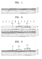
FIGS. 1 through 5 are sectional views showing a first masking operation of a method of manufacturing a flat panel display apparatus, according to an embodiment of the present invention; -
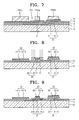
FIGS. 6 through 9 are sectional views showing a second masking operation of the method of manufacturing a flat panel display apparatus, according to an embodiment of the present invention; -
FIGS. 10 and 11 are sectional views showing a third masking operation of the method of manufacturing a flat panel display apparatus, according to an embodiment of the present invention; -
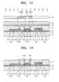
FIGS. 12 and 13 are sectional views showing a fourth masking operation of the method of manufacturing a flat panel display apparatus, according to an embodiment of the present invention; -
FIGS. 14 and 15 are sectional views showing a fifth masking operation of the method of manufacturing a flat panel display apparatus, according to an embodiment of the present invention; -
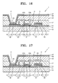
FIG. 16 is a sectional view showing a flat panel display apparatus according to an embodiment of the present invention; -
FIG. 17 is a sectional view showing a flat panel display apparatus according to a modified embodiment of the present invention; -
FIGS. 18 through 20 are sectional views showing a first masking operation of a method of manufacturing a flat panel display apparatus, according to another embodiment of the present invention; -
FIG. 21 is a sectional view showing a flat panel display apparatus according to another embodiment of the present invention; and -
FIG. 22 is a sectional view showing a flat panel display apparatus according to another modified embodiment of the present invention. - Reference will now be made in detail to embodiments of the present invention, examples of which are illustrated in the accompanying drawings, wherein like reference numerals refer to the like elements throughout. The embodiments are described below in order to explain the present invention by referring to the figures.
- As referred to herein, when a first element is said to be disposed or formed "on" a second element, the first element can directly contact the second element, or can be separated from the second element by one or more other elements located therebetween. In contrast, when an element is referred to as being disposed or formed "directly on" another element, there are no intervening elements present.
- First, referring to
FIGS. 1 through 16 , a flat panel display apparatus according to an embodiment of the present invention will be described. -
FIGS. 1 through 15 are sectional views roughly showing a method of manufacturing an organic light emitting diode (OLED) display apparatus, according to an embodiment of the present invention, andFIG. 16 is a sectional view roughly showing anOLED display apparatus 1 fabricated using the method illustrated inFIGS. 1 through 15 , according to an embodiment of the present invention. - Referring to
FIG. 16 , theOLED display apparatus 1 according to the current embodiment includes asubstrate 10, abuffer layer 11, a thin-film transistor (TFT) 2, acapacitor 3, and anOLED 4. - First, referring to
FIG. 1 , thebuffer layer 11, asemiconductor layer 12, and a firstconductive layer 13 are sequentially formed on thesubstrate 10. - The
substrate 10 may be formed of a transparent glass material primarily composed of SiO2. However, aspects of the present invention are not limited thereto, and thesubstrate 10 may be formed of an opaque glass material, plastics, or other such materials. However, if theOLED display apparatus 1 is a bottom emission type OLED display apparatus in which images of theOLED display apparatus 1 are viewed below thesubstrate 10, thesubstrate 10 should be formed of a transparent material. - The
buffer layer 11 may be disposed on the top surface of thesubstrate 10 to smooth thesubstrate 10 and to preventing impurities from penetrating into thesubstrate 10. Thebuffer layer 11 may be formed of SiO2 and/or SiNx, and may be deposited by using a deposition method such as plasma enhanced chemical vapor deposition (PECVD), atmospheric pressure CVD (APCVD), low pressure CVD (LPCVD), or other similar deposition methods. - The
semiconductor layer 12 may be formed of poly-crystal silicon crystallized after depositing amorphous silicon. The amorphous silicon may be crystallized by rapid thermal annealing (RTA), solid phase crystallization (SPC), excimer laser annealing (ELA), metal induced crystallization (MIC), metal induced lateral crystallization (MILC), sequential lateral solidification (SLS), or the like. - The first
conductive layer 13 is formed on thesemiconductor layer 12. According to the present embodiment, the firstconductive layer 13 is formed by depositing amorphous silicon containing n-type or p-type impurities and performing a heat treatment process on the amorphous silicon. However, aspects of the present invention are not limited thereto, and the firstconductive layer 13 may include any material containing a metal. - Referring to
FIG. 2 , photoresist is applied to the top surface of the structure shown inFIG. 1 , and a first photoresist layer P1 is formed by either pre-baking or soft-baking the photoresist. Next, a first mask M1 on which a predetermined pattern is printed is prepared and aligned on thesubstrate 10 for patterning the first photoresist layer P1. - The first mask M1 is a half-tone mask including a photo-transmissive region M11, a photo-interceptive region M12, and a semi photo-transmissive region M13. The photo-transmissive region M11 transmits light of wavelengths in a predetermined range. The photo-interceptive region M12 blocks irradiated light. The semi photo-transmissive region M13 transmits only some of the irradiated light.
-
FIG. 2 is a concept view describing concepts of each of the regions of the first mask M1. The first mask M1 may be formed as a predetermined pattern on a transparent substrate, such as a quartz (Qz) substrate. Here, the photo-interceptive region M12 is formed by patterning materials such as Cr or CrO2 on the quartz substrate, and the semi photo-transmissive region M13 may be formed of at least one of Cr, Si, Mo, Ta, and Al. Photo-transmissivity of the semi photo-transmissive region M13 may be controlled by changing composition ratio and/or thickness of materials forming the semi photo-transmissive region M13. - The first mask M1 on which a pattern as described above is printed is aligned on the
substrate 10, and a photolithographic operation is performed by irradiating light of wavelengths in a predetermined range onto the first photoresist layer P1. -
Figure 3 shows a pattern of the first photoresist layer P1 remaining after removing exposed portions of the first photoresist layer P1. Although positive photoresist, of which exposed portions are removed, is used in the current embodiment, aspects of the present invention are not limited thereto, and negative photoresist can also be used. - Referring to
FIG. 3 , a portion P11 of the photoresist layer P1 corresponding to the photo-transmissive region M11 of the first mask M1 is removed, whereas a portion P12 of the first photoresist layer P1 corresponding to the photo-interceptive region M12 and a portion P13 of the first photoresist layer P1 corresponding to the semi photo-transmissive region M13 remain. At this point, the thickness of the portion P13 of the first photoresist layer P1 corresponding to the semi photo-transmissive region M13 is less than that of the portion P12 of the first photoresist layer P1 corresponding to the photo-interceptive region M12, and the thickness of the portion P13 may be controlled by changing the composition ratio and/or thickness of materials forming the semi photo-transmissive region M13. - The
semiconductor layer 12 and the firstconductive layer 13 on thesubstrate 10 are etched using etching equipment, wherein the portions P12 and P13 of the first photoresist layer P1 are used as etching masks. In this regard, the region P11 is etched first, and the thickness of the region P13 of the first photoresist layer P1 is reduced by etching. Here, the etching operation may comprise wet etching, dry etching, or the like, however, aspects of the present invention are not limited thereto. - Referring to
FIG. 4 , while a first etching operation is being performed, portions of thesemiconductor layer 12 and the firstconductive layer 13 ofFIG. 3 corresponding to the portion P11 of the first photoresist layer P1 are etched. Furthermore, although the portion P13 of the photoresist layer P13 corresponding to the semi photo-transmissive region M13 ofFIG. 3 is etched, structures below the portion P13 of the photoresist layer P13 remain. Meanwhile, the portion P12 of the first photoresist layer P1 corresponding to the photo-interceptive region M12 partially remains after the first etching operation, and a second etching operation is performed by using the remainder of the portion P12 of the first photoresist layer P1 as an etching mask. - Referring to
FIG. 5 , the remainder of the portion P12 of the photoresist layer P1, which remained after the first etching operation, and the firstconductive layer 13 in the region corresponding to the semi photo-transmissive region M13, are completely etched in the second etching operation. As a result, afirst electrode 31 and anactive layer 21 are formed on thebuffer layer 11, wherein thefirst electrode 31 includes a first bottom electrode 31-1 including a portion of thesemiconductor layer 12 and a first top electrode 31-2 including a portion of the firstconductive layer 13, and theactive layer 21 includes a portion of thesemiconductor layer 12. The first bottom electrode 31-1 and the first top electrode 31-2 constitute a capacitor, and theactive layer 21 is part of a TFT - The
active layer 21 of the TFT and the first bottom electrode 31-1 and the first top electrode 31-2 of the capacitor are simultaneously patterned on a same structure by using the same mask M1, and thus theactive layer 21 of the TFT and the first bottom electrode 31-1 of the capacitor are formed of the same material and are formed on the same layer. Furthermore, since they are simultaneously patterned by using the same mask M1, shapes of ends of the capacitor formed by the first bottom electrode 31-1 and the first top electrode 31-2 are the same. - Referring to
FIG. 6 , afirst insulation layer 14, a secondconductive layer 15, and a thirdconductive layer 16 are sequentially formed on the structure ofFIG. 5 , which is the result of the first masking operation. A second photoresist layer P2 is formed on the thirdconductive layer 16, and a second mask M2 is aligned on thesubstrate 10. - The
first insulation layer 14 may be formed by depositing an inorganic insulation material using a deposition method such as PECVD, APCVD, LPCVD, or the like, wherein the inorganic insulation material comprises a material such as SiNx or SiOx. A portion of thefirst insulation layer 14 is interposed between theactive layer 21 and a gate bottom electrode 22-1 of a TFT 2 (to be described later) and functions as a gate insulation layer of theTFT 2, whereas another portion of thefirst insulation layer 14 is interposed between the first top electrode 31-2 and a second bottom electrode 32-1 of a capacitor 3 (to be described later) and functions as a first dielectric layer. - The second
conductive layer 15 may contain one or more transparent materials such as ITO, IZO, ZnO, and In203. As shown inFIG. 8 , the secondconductive layer 15 constitutes a pixel bottom electrode 42-1 of a flat panel display, a gate bottom electrode 22-1 of theTFT 2, and the second bottom electrode 32-1 of thecapacitor 3. Although the secondconductive layer 15 is formed as a single layer in the current embodiment, aspects of the present invention are not limited thereto, and a plurality of conductive layers may be formed. In other words, when a pixel electrode 42 (to be described later) is only formed of transparent materials as in the current embodiment, thepixel electrode 42 can be used in a bottom-emission type display apparatus in which images are viewed from below thesubstrate 10. However, in the case of a top-emission type display apparatus, a reflective layer may be formed by forming the plurality of second conductive layers and depositing transparent conductive materials thereon, wherein the transparent conductive materials are as materials used in the current embodiment. Furthermore, more than two layers may be formed if required, however, aspects of the present invention are not limited thereto. - The third
conductive layer 16 may contain one or more materials from among Ag, Mg, Al, Pt, Pd, Au, Ni, Nd, Ir, Cr, Li, Ca, Mo, Ti, W, MoW, and Al/Cu. The thirdconductive layer 16 constitutes a pixel top electrode 42-2 of a flat panel display, a gate top electrode 22-2 of theTFT 2, and a second top electrode 32-2 of thecapacitor 3. - The second mask M2 includes a photo-transmissive region M21 and photo-interceptive regions M22a, M22b, and M22c in predetermined patterns. The second mask M2 is aligned on the
substrate 10, and light of wavelengths in a predetermined range is irradiated onto the second photoresist layer P2. - Referring to
FIG. 7 , a portion P21 of the second photoresist layer P2 corresponding to the photo-transmissive region M21 of the second mask M2 is removed, whereas portions P22a, P22b, and P22c of the second photoresist layer P2, which respectively correspond to the photo-interceptive regions M22a, M22b, and M22c, remain. - The portions P22a, P22b, and P22c of the second photoresist layer P2 are used as masks to etch the second
conductive layer 15 and the thirdconductive layer 16 on thesubstrate 10 using etching equipment, in a second masking operation. The etching operation described above may comprise wet etching, dry etching, or the like, however, aspects of the present invention are not limited thereto. - Referring to
FIG. 8 , a structure obtained after the etching operation in the second masking operation, is shown. Portions of the secondconductive layer 15 and the thirdconductive layer 16 in the region P21 of the second photoresist layer P2, which is a region from which the second photoresist layer P2 is removed, are etched. In the regions where the second photoresist layer P2 remains, a double-layeredgate electrode 22 is patterned to correspond to the center region of theactive layer 21 of theTFT 2. Using a pattern of the double-layeredgate electrode 22, either n-type or p-type impurities are implanted into edges of theactive layer 21 of theTFT 2. -
Figure 9 shows a structure obtained after etching and ion implanting operations are performed in the second masking operation, is shown. Theactive layer 21 of theTFT 2 includes asource region 21 a, adrain region 21 b, and achannel region 21 c that are formed by the ion implantation. The double-layeredgate electrode 22, double-layered first andsecond electrodes capacitor 3, and a double-layered pixel electrode 42 are formed at a location corresponding to thechannel region 21 c of theTFT 2. - Referring to
FIG. 9 , the double-layered pixel electrode 42, thegate electrode 21 of theTFT 2, and thesecond electrode 32 of thecapacitor 3 are simultaneously patterned on the same structure using the same second mask M2. Thus, the pixel bottom electrode 42-1, the gate bottom electrode 21-1 of theTFT 2, and the second bottom electrode 32-1 are formed of the same material and formed on the same layer, whereas the pixel top electrode 42-2, the gate top electrode 21-2 of theTFT 2, and the second top electrode 32-2of thecapacitor 3 are formed of the same material and formed on the same layer. Furthermore, shapes of ends of each of the pixel bottom electrode 42-1 and the pixel top electrode 42-2, ends of the gate bottom electrode 22-1 and the gate top electrode 22-2, and ends of the second bottom electrode 32-1 and the second top electrode 32-2 of thecapacitor 3 are the same. - Referring to
FIG. 10 , asecond insulation layer 17 is formed on the structure shown inFIG. 9 , which is a result of the second masking operation. A third photoresist layer P3 is formed on thesecond insulation layer 17, and a third mask M3 is aligned on thesubstrate 10. - The
second insulation layer 17 may be formed of one or more organic insulation materials, such as polyimide, polyamide, acryl resin, and phenol resin, using a method such as spin coating. Thesecond insulation 17 is formed to have a thickness sufficient to function as an interlayer insulation layer between the double-layeredgate electrode 22 of the thin-film transistor (TFT) 2 and asource electrode 24a and adrain electrode 24b described below. Meanwhile, thesecond insulation layer 17 may be formed of not only organic insulation materials as described above, but also inorganic insulation materials as thefirst insulation layer 14 described above. Furthermore, thesecond insulation layer 17 may also be formed by alternating organic insulation materials and inorganic insulation materials of an alternate structure of organic insulation materials and inorganic insulation materials. - The third mask M3 is patterned to include photo-transmissive regions M31 a, M31 b, and M31 c and a photo-interceptive region M32, corresponding to portions of the
source region 21 a and thedrain region 21 b and portions of the edges of thepixel electrode 42. The third mask M3 including the patterns described above is aligned on thesubstrate 10, and a photolithographic operation is performed thereon. -
FIG. 11 illustrates the resulting structure after an etching operation using the remaining portions of the third photoresist layer P3 as etching masks is performed, wherein the remaining portions remain after exposed portions of the third photoresist layer P3 are removed. This is referred to as a third masking operation.Openings source region 21 a and thedrain region 21 b and a region corresponding to the portions of the edges of the pixel top electrode 42-2, are formed. From among theopenings openings source region 21 a and thedrain region 21 b constitute contact holes, whereas theopening 23c formed in the region corresponding to the portions of the edges of the pixel top electrode 42-2 constitutes a via hole. However, aspects of the present invention are not limited to such names. - Referring to
FIG. 12 , a fourthconductive layer 18 is formed on the structure ofFIG. 11 , which is a result of the third masking operation. A fourth photoresist layer P4 is formed on the fourthconductive layer 18, and a fourth mask M4 is aligned on thesubstrate 10. - Although the fourth
conductive layer 18 may be formed of the material used to form the secondconductive layer 15 and/or the thirdconductive layer 16 described above, aspects of the present invention are not limited thereto, and the fourthconductive layer 18 may be formed of various conductive materials. Furthermore, the conductive materials are deposited to a thickness sufficient to fill theopenings - The fourth mask M4 includes a photo-transmissive region M41 and photo-interceptive regions M42a and M42b. After a photolithographic operation is performed on the fourth photoresist layer P4 and the fourth photoresist layer P4 is developed, remaining portions of the fourth photoresist layer P4 are used as etching masks for an etching operation in a fourth masking operation.
- Referring to
FIG. 13 , as a result of the fourth masking operation, thesource electrode 24a and thedrain electrode 24b, which respectively contact thesource region 21 a and thedrain region 21 b via thecontact holes second insulation layer 17. Furthermore, one of thesource electrode 24a and thedrain electrode 24b is formed to be connected to the pixel top electrode 42-2 via the viahole 23c, wherein the viahole 23c is connected to a portion of the edge regions of the pixel top electrode 42-2. - Referring to
FIG. 14 , athird insulation layer 19 is formed on the structure illustrated inFIG. 13 , which is a result of the fourth masking operation, and a fifth mask M5 is aligned on thesubstrate 10. - The
third insulation layer 19 may be formed of one or more organic insulation materials, such as polyimide, polyamide, acryl resin, and phenol resin, using a method such as spin coating. Meanwhile, thethird insulation layer 19 may be formed of organic insulation materials as described above, and also the inorganic insulation materials used to form thefirst insulation layer 14 and thesecond insulation layer 17 described above. Thethird insulation layer 19 functions as a pixel defining layer (PDL) 43 of theOLED apparatus 1 described below, after an etching operation is performed using the fifth mask M5. - The fifth mask M5 includes a photo-transmissive region M51 formed in a portion thereof corresponding to the double-
layered pixel electrode 42 and a photo-interceptive region M52 formed in remaining portions thereof. - Referring to
FIG. 15 , after the etching operation ofFIG. 14 is performed, thesecond insulation layer 17, thethird insulation layer 19, and the pixel top electrode 42-2 in a region corresponding to the photo-transmissive region M51 are etched, and thus the pixel bottom electrode 42-1 is exposed. Thesecond insulation layer 17 and thethird insulation layer 19 are sequentially stacked on the edge of the pixel top electrode 42-2 around anopening 44 formed in the etching operation above. At this point, thethird insulation layer 19, which is formed to have a predetermined thickness along theopening 44, widens an interval between the edge of the double-layered pixel electrode 42 and anopposite electrode 47 described below to prevent concentration of electric field at the edge of thepixel electrode 42. In other words, thethird insulation layer 19 functions as thePDL 43 preventing a short between apixel electrode 42 and an opposite electrode which is the two-way electrode 47. - Referring to
FIG. 16 , anintermediate layer 46, which includes an organiclight emitting layer 45, and the two-way electrode 47 are formed on the exposed portion of the pixel bottom electrode 42-1 and thePDL 43. - The organic
light emitting layer 45 emits light when electrically driven by the double-layered pixel electrode 42 and the two-way electrode 47. The organiclight emitting layer 45 may be formed of either a low molecular organic material or a high molecular organic material. - If the organic
light emitting layer 45 is formed of a low molecular organic material, theintermediate layer 46 may include a hole transport layer (HTL) and a hole injection layer (HIL) stacked toward thepixel electrode 42, and an electron transport layer (ETL) and an electron injection layer (ElL) stacked toward the two-way electrode 47. Furthermore, various other layers may be stacked if required. Further, various organic materials such as copper phthalocyanine (CuPc), N,N'-Di(naphthalene-1-yl)-N,N'-diphenyl-benzidine, tris-8-hydroxyquinoline aluminum (Alq3), etc., may be used as the organiclight emitting layer 45. - Meanwhile, If the organic
light emitting layer 45 is formed of a high molecular organic material, theintermediate layer 46 may include only the HTL formed toward thepixel electrode 42 from the organiclight emitting layer 43. The HTL may be formed of poly-(2,4)-ethylene-dihydroxy thiophene (PEDOT), polyaniline (PANI), etc., and may be formed on the top surface of thepixel electrode 42 using a method such as inkjet printing or spin coating. Here, organic materials may be high molecular organic materials such as a poly-phenylenevinylene material or a polyfluorene material, and a color pattern may be formed by using a general method such as inkjet printing, spin coating, or heat transference using a laser. - The two-
way electrode 47 is formed on theintermediate layer 46 including the organiclight emitting layer 45, as a common electrode. In the case of theOLED apparatus 1 according to the current embodiment, thepixel electrode 42 is used as an anode electrode, whereas the two-way electrode 47 that is formed as a common electrode is used as a cathode electrode. However, aspects of the present invention are not limited thereto and the polarity of thepixel electrode 42 and the two-way electrode 47 that is formed as a common electrode may be reversed. - If the
OLED apparatus 1 is a bottom emission type OLED device in which images are displayed below thesubstrate 10, thepixel electrode 45 becomes a transparent electrode and the two-way electrode 47 that is formed as a common electrode becomes a reflective electrode. Here, the reflective electrode may be formed by depositing a thin layer of metal with a small work function, such as Ag, Mg, Al, Pt, Pd, Au, Ni, Nd, Ir, Cr, Li, Ca, LiF/Ca, LiF/Al, or a compound thereof. - Furthermore, although not illustrated in
FIG. 16 , a sealant and a moisture absorbent may further be disposed on the two-way electrode 47 that is formed as a common electrode for protecting the organiclight emitting layer 45 from external moisture or oxygen. - According to the OLED apparatus and the method of manufacturing the same according to the embodiment described above, an OLED apparatus can be manufactured by using a small number of masks. Therefore, manufacturing costs can be reduced and the manufacturing process can be simplified due to a reduction in the number of masks required.
- Meanwhile, although an operation using a half-tone mask is employed to reduce the number of masks required, the half-tone mask is used only once, and thus a cost increase due to the use of the half-tone mask can be minimized.
- Furthermore, the pixel electrode is kept protected by the second insulation layer and the third insulation layer, and is exposed right before the organic light emitting layer is formed. Thus, damage to the pixel electrode can be prevented, as compared to conventional methods of manufacturing OLED apparatuses in which manufacturing operations are performed while pixel electrodes are exposed.
-
FIG. 17 is a cross-sectional view of an OLED apparatus 1' according to another embodiment of the present invention. - The OLED apparatus 1' according to the current embodiment includes the
substrate 10, thebuffer layer 11, and theTFT 2 of the previous embodiment, a capacitor 3', and anOLED 4. The structure of the capacitor 3' in the OLED apparatus 1' according to the current embodiment is different from the structure of thecapacitor 3 in theOLED apparatus 1. The description below will focus on this difference. - The capacitor 3' of the OLED apparatus 1', according to the current embodiment, includes a
third electrode 33. Thethird electrode 33 of the capacitor 3' is formed on a portion of thesecond insulation layer 17 corresponding to the second top electrode 32-2 of the capacitor 3'. Thethird electrode 33 of the capacitor 3' is formed of the material used to form the source electrode and thedrain electrode - In other words, although not shown in
FIG. 17 , a photolithographic operation is performed on the portion of thesecond insulation layer 17 corresponding to the second top electrode 32-2 of the capacitor 3' by using a mask pattern. The photo-interceptive region is formed in the portion of thesecond insulation layer 17 in the fourth masking operation to fabricate the capacitor 3' according to the current embodiment. - According to the above-described structure, the capacitance of the capacitor 3' of the
OLED apparatus 1 increases, and thus the increased capacitance of the capacitor 3' contributes not only to the cost reduction due to reduction of mask usage and pixel electrode damage prevention, but also to display quality of the OLED apparatus 1'. - Hereinafter, a method of manufacturing an OLED apparatus according to another embodiment of the present invention will be described by referring to
FIGS. 18 through 21. FIGS. 18 through 21 are cross-sectional views illustrating another method of manufacturing an OLED apparatus. - The OLED apparatus 1' includes the
substrate 10, thebuffer layer 11, thecapacitor 3 and theOLED 4 of the embodiment illustrated inFIGS. 1 through 16 , and a TFT 2'. The structure of the TFT 2' in the OLED apparatus 1', according to the current embodiment, is different from the structure of theTFT 2 in theOLED apparatus 1. The description below will focus on this difference. - First, referring to
FIG. 18 , a first photoresist layer P1' is formed on the structure illustrated inFIG. 1 , and a first mask M1' on which a predetermined pattern is printed is aligned on thesubstrate 10 to pattern the first photoresist layer P1'. - The first mask M1' is a half-tone mask including a photo-transmissive region M11', photo-interceptive regions M12a', M12b', and M12c', and a semi photo-transmissive region M13'.
- The first mask M1' including the pattern described above is aligned on the
substrate 10, and a photolithographic operation is performed by irradiating light of wavelengths in a predetermined range on the first mask M1'. -
Figure 19 shows a pattern of the first photoresist layer P1' remaining after a developing process is performed, by which exposed portions of the photoresist layer P1' are removed. A portion P11' of the first photoresist layer P1' corresponding to the photo-transmissive M11' of the first mask M1' is removed, whereas portions P12a', P12b', and P12c' of the first photoresist layer P1' respectively corresponding to the photo-interceptive regions M12a', M12b', and M12c' and a portion P13' of the first photoresist layer P1' corresponding to the semi photo-transmissive region M13' remain. - Using the portions P12a', P12b', and P12c' as masks, the
semiconductor layer 12 and the firstconductive layer 13 on thesubstrate 10 are etched by using etching equipment. In this regard, exposed portions of thesemiconductor layer 12 and the firstconductive layer 13 from which the first photoresist layer P1' has been removed are etched first, and the thickness of the first photoresist layer P1' is reduced by being etched. Here, the etching operation may comprise wet etching, dry etching, or the like. - Referring to
FIG. 20 , while a first etching operation is being performed, portions of thesemiconductor layer 12 and the firstconductive layer 13, shown inFIG. 19 , in the portion P11 are etched. Furthermore, referring toFIG. 20 , although the portion P13' of the first photoresist layer P1' corresponding to the semi photo-transmissive region M13' is etched, structures below the portion P13' remain. Meanwhile, the portions P12a', P12b', and P12c' of the first photoresist layer P1' respectively corresponding to the photo-interceptive regions M12a, M12b, and M12c partially remain after the first etching operation, and a second etching operation is performed by using them as etching masks. -
FIG. 21 shows a shape of the OLED apparatus 1' after the remaining portions P12a', P12b', and P12c' illustrated inFIG. 20 are completely etched after the second etching operation and then the second through fourth masking operations are completed. - A portion of the first
conductive layer 13 below a region in which the first photoresist layer P1' is partially removed (between P12a' and P12b'), is partially etched, and portions of the firstconductive layer 13 below remaining regions (below P12a' and P12b') constitute thesource region 21a' and thedrain region 21b' of the TFT 2'. - According to the
OLED apparatus 2, according to the current embodiment described above, the source region and the drain region are formed during an etching operation using the first mask M1'. In other words, a separate ion implanting operation is not necessary, unlike in the previous embodiment of the present invention, and thus the manufacturing process can be simplified. -
FIG. 22 is a cross-sectional view of an OLED apparatus according to yet another embodiment of the present invention. - Referring to
FIG. 22 , the OLED apparatus, according to the current embodiment, includes thesubstrate 10, thebuffer layer 11, the TFT 2', the capacitor 3', and theOLED 4. Structures of the TFT 2' and the capacitor 3' in the OLED apparatus, according to the current embodiment, are different from the structures of theTFT 2 and thecapacitor 3 in theOLED apparatus 1 according to the embodiment illustrated inFIGS. 1 through 16 . - As in the OLED apparatus 1', according to the previous embodiment, the TFT 2' includes the
source region 21 a' and thedrain region 21 b' that are formed of the material used to form the first top electrode 31-2 of thecapacitor 3 during the first masking operation. - Meanwhile, as in the OLED apparatus 1' according to the previous embodiment, the capacitor 3' further includes the
third electrode 33 of the capacitor 3' that is formed of the material used to form thesource electrode 24a and thedrain electrode 24b during the fourth masking operation. - According to the OLED apparatus according to the current embodiment, a separate ion implanting operation for forming the source region and the drain region is not necessary, and thus the overall manufacturing process is simplified. Furthermore, the capacitance of the capacitor 3' increases, and thus the increased capacitance of the capacitor 3' contributes to the cost reduction due to reduction of mask usage and pixel electrode damage prevention and also to display quality of the OLED apparatus.
- Meanwhile, although an OLED apparatus is used as an example of a flat panel display apparatus in the embodiments described above, aspects of the present invention are not limited thereto, and various display devices such as a liquid crystal display (LCD) device, etc. can be used.
- Furthermore, although one TFT and one capacitor are illustrated in
FIGS. 1 through 22 for convenience of explanation, aspects of the present invention are not limited thereto. Thus, it is clear that a plurality of TFTs and a plurality of capacitors can be included. - Although a few embodiments of the present invention have been shown and described, it would be appreciated by those skilled in the art that changes may be made without departing from the principles of the invention, the scope of which is defined in the claims and their equivalents.
Claims (22)
- A flat panel display apparatus comprising:a substrate;an active layer of a thin film transistor (TFT), comprising:a channel region;a source region; anda drain region;a first bottom electrode of a capacitor formed apart from the active layer on the same layer as the active layer and formed of a same material as at least part of the active layer and a first top electrode of a capacitor formed on the first bottom electrode;a first insulation layer formed on the substrate, the active layer, and the first top electrode;a gate bottom electrode and a gate top electrode sequentially formed on a portion of the first insulation layer corresponding to the channel region;a second bottom electrode and a second top electrode of the capacitor formed of the same material used to form the gate bottom electrode and the gate top electrode, wherein the second bottom electrode and the second top electrode are sequentially formed on a portion of the first insulation layer corresponding to the first top electrode of the capacitor;a pixel bottom electrode formed of the same material used to form the gate bottom electrode and the second bottom electrode of the capacitor and formed on the first insulation layer;a pixel top electrode formed of the same material as that used to form the gate top electrode and the second top electrode of the capacitor and formed in an edge region of a top surface of the pixel bottom electrode to expose the pixel bottom electrode;a second insulation layer formed on the gate electrode, the second electrode of the capacitor, and the pixel top electrode and penetrated by contact holes respectively exposing the source region and the drain region of the active layer and a via hole exposing an edge portion of the pixel top electrode; anda source electrode and a drain electrode formed on the second insulation layer; the source electrode being connected to the source region via one of the contact holes and the drain electrode being connected to the drain region via the other of the contact holes and the pixel top electrode via the via hole.
- A flat panel display apparatus according to claim 1, further comprising:a pixel defining layer formed on the second insulation layer and exposing the pixel bottom electrode;an intermediate layer formed on the pixel bottom electrode and comprising an organic light emitting layer; andan opposite electrode formed on the intermediate layer.
- A flat panel display apparatus according to claim 1 or 2, wherein the active layer of the TFT and the first bottom electrode of the capacitor comprise polysilicon.
- A flat panel display apparatus according to claim 1, 2 or 3, wherein the first top electrode of the capacitor contains silicon into which impurities are implanted.
- A flat panel display apparatus according to any preceding claim, wherein the shapes of the first bottom electrode and the first top electrode of the capacitor are substantially the same.
- A flat panel display apparatus according to any preceding claim, wherein the shapes of the gate bottom electrode and the gate top electrode are substantially the same.
- A flat panel display apparatus according to any preceding claim, wherein the shapes of the second bottom electrode and the second top electrode of the capacitor are substantially the same.
- A flat panel display apparatus according to any preceding claim, wherein the shapes of the pixel bottom electrode and the pixel top electrode are substantially the same.
- A flat panel display apparatus according to any preceding claim, further comprising a buffer layer on the substrate.
- A flat panel display apparatus according to any preceding claim, wherein the thickness of the second insulation layer is greater than that of the first insulation layer.
- A flat panel display apparatus according to any preceding claim, further comprising a third electrode of the capacitor, which is formed of the same material as that used to form the source electrode and the drain electrode and is formed on the second insulation layer to correspond to the second top electrode of the capacitor.
- A flat panel display apparatus according to any preceding claim wherein the channel region, the source region and the drain region are formed on the same layer on the substrate.
- A flat panel display apparatus according to one of Claims 1 to 11 wherein the source region and the drain region are formed on a top surface of the channel region.
- A flat panel display apparatus according to any preceding claim, wherein the capacitor comprises a third electrode which is formed of the same material as that used to form the source electrode and the drain electrode and is formed on the second insulation layer to correspond to the second top electrode of the capacitor.
- A method of manufacturing a flat panel display apparatus, the method comprising:sequentially forming a semiconductor layer and a first conductive layer on a substrate;simultaneously patterning the semiconductor layer and the first conductive layer to form an active layer of a thin-film transistor (TFT) and a capacitor having a first bottom electrode and a first top electrode in a first masking operation;forming a first insulation layer on a structure formed by the first masking operation;sequentially forming a second conductive layer and a third conductive layer on the first insulation layer;simultaneously patterning each of the second conductive layer and the third conductive layer to respectively form a gate bottom electrode and a gate top electrode of the TFT, to form a second bottom electrode and a second top electrode of the capacitor, and to form a pixel bottom electrode and a pixel top electrode in a second masking operation;forming a second insulation layer on a structure formed by the second masking operation;patterning the second insulation layer to partially expose the source region and the drain region and edges of the pixel top electrode in a third masking operation;forming a fourth conductive layer on a structure formed by the third masking operation;patterning the fourth conductive layer to form a source electrode and a drain electrode of the TFT in a fourth masking operation;forming a third insulation layer on a structure formed by the fourth masking operation; andremoving the second insulation layer and the third insulation layer, such that the pixel top electrode is exposed, in a fifth masking operation.
- A method according to claim 15, wherein a first mask of the first masking operation is a half-tone mask comprising a semi photo-transmissive region in a portion thereof corresponding to the active layer of the TFT.
- A method according to Claim 16, wherein the location of the semi photo-transmissive region corresponds to a center region of the active layer of the TFT.
- A method according to claim 16 or 17, wherein the half-tone mask is used only once.
- A method according to one of Claims 15 to 18, further comprising sequentially forming an intermediate layer comprising an organic light emitting layer and an opposite electrode on a structure formed by the fifth masking operation.
- A method according to one of Claims 15 to 19, further comprising forming a buffer layer on the substrate.
- A method according to one of Claims 15 to 20, wherein the fourth masking operation comprises an operation for simultaneously patterning the third electrode of the capacitor, the source electrode, and the drain electrode to form the fourth conductive layer.
- A method according to one of Claims 15 to 21, further comprising forming a source region and a drain region in edges of the active layer of the TFT by using the gate bottom electrode and the gate top electrode as a self-aligned mask.
Applications Claiming Priority (1)
| Application Number | Priority Date | Filing Date | Title |
|---|---|---|---|
| KR1020090007385A KR101074788B1 (en) | 2009-01-30 | 2009-01-30 | Flat panel display apparatus and the manufacturing method thereof |
Publications (3)
| Publication Number | Publication Date |
|---|---|
| EP2214211A2 true EP2214211A2 (en) | 2010-08-04 |
| EP2214211A3 EP2214211A3 (en) | 2013-07-31 |
| EP2214211B1 EP2214211B1 (en) | 2016-09-28 |
Family
ID=42236517
Family Applications (1)
| Application Number | Title | Priority Date | Filing Date |
|---|---|---|---|
| EP10250161.6A Active EP2214211B1 (en) | 2009-01-30 | 2010-01-29 | Flat panel display apparatus and method of manufacturing the same |
Country Status (5)
| Country | Link |
|---|---|
| US (1) | US8106402B2 (en) |
| EP (1) | EP2214211B1 (en) |
| JP (1) | JP5202554B2 (en) |
| KR (1) | KR101074788B1 (en) |
| CN (1) | CN101794049B (en) |
Cited By (5)
| Publication number | Priority date | Publication date | Assignee | Title |
|---|---|---|---|---|
| DE102011005528B4 (en) * | 2010-05-17 | 2013-11-21 | Samsung Display Co., Ltd. | Production method of an organic light-emitting display device |
| EP2463911A3 (en) * | 2010-12-08 | 2014-01-15 | Samsung Display Co., Ltd. | Organic light emitting display device and manufacturing method for the same |
| EP2500946A3 (en) * | 2011-03-14 | 2014-03-05 | Samsung Display Co., Ltd. | Organic light-emitting display and method of manufacturing the same |
| GB2492607B (en) * | 2010-09-20 | 2014-10-22 | Lg Display Co Ltd | Organic light emitting diode display and method for manufacturing the same |
| WO2016170355A1 (en) * | 2015-04-22 | 2016-10-27 | Flexenable Limited | A control component for a current-driven optical media |
Families Citing this family (108)
| Publication number | Priority date | Publication date | Assignee | Title |
|---|---|---|---|---|
| KR20110024531A (en) * | 2009-09-02 | 2011-03-09 | 삼성모바일디스플레이주식회사 | Organic light emitting display device |
| KR101084277B1 (en) * | 2010-02-03 | 2011-11-16 | 삼성모바일디스플레이주식회사 | OLED display and manufacturing method thereof |
| KR101056429B1 (en) | 2010-03-16 | 2011-08-11 | 삼성모바일디스플레이주식회사 | Display device and manufacturing method thereof |
| KR101210146B1 (en) * | 2010-04-05 | 2012-12-07 | 삼성디스플레이 주식회사 | Display device and Method of manufacturing the same |
| KR101234230B1 (en) * | 2010-06-17 | 2013-02-18 | 삼성디스플레이 주식회사 | Organic light emitting display device and manufacturing method of the same |
| KR101193197B1 (en) * | 2010-07-07 | 2012-10-19 | 삼성디스플레이 주식회사 | Organinc light emitting display device and manufacturing method for the same |
| KR101777246B1 (en) * | 2010-08-30 | 2017-09-12 | 삼성디스플레이 주식회사 | Organic light emitting display device and manufacturing method of the same |
| KR101323555B1 (en) * | 2010-09-20 | 2013-10-29 | 엘지디스플레이 주식회사 | Organic Light Emitting Display Device And Manufacturing Method Of The Same |
| KR101780250B1 (en) * | 2010-09-24 | 2017-09-22 | 삼성디스플레이 주식회사 | Organinc light emitting display device and manufacturing method for the same |
| KR101746617B1 (en) | 2010-09-24 | 2017-06-28 | 삼성디스플레이 주식회사 | Organic light emitting display device and manufacturing method of the same |
| KR101777247B1 (en) | 2010-09-29 | 2017-09-12 | 삼성디스플레이 주식회사 | Organic light emitting display device and manufacturing method of the same |
| KR101372852B1 (en) | 2010-10-05 | 2014-03-10 | 삼성디스플레이 주식회사 | Organic light emitting display device and manufacturing method of the same |
| KR20120039946A (en) * | 2010-10-18 | 2012-04-26 | 삼성모바일디스플레이주식회사 | Organic light emitting display device and method for manufacturing the same |
| KR101782557B1 (en) * | 2010-10-25 | 2017-09-28 | 삼성디스플레이 주식회사 | Organic light emitting display device and manufacturing method of the same |
| KR20120043404A (en) * | 2010-10-26 | 2012-05-04 | 삼성모바일디스플레이주식회사 | Display apparatus and method of manufacturing the same |
| KR101811702B1 (en) * | 2010-10-27 | 2017-12-26 | 삼성디스플레이 주식회사 | Organinc light emitting display device and manufacturing method for the same |
| KR101711191B1 (en) * | 2010-10-28 | 2017-03-02 | 삼성디스플레이 주식회사 | Organic light emitting display device and manufacturing method thereof |
| US8936965B2 (en) * | 2010-11-26 | 2015-01-20 | Semiconductor Energy Laboratory Co., Ltd. | Semiconductor device and manufacturing method thereof |
| KR101807849B1 (en) | 2010-12-08 | 2017-12-12 | 삼성디스플레이 주식회사 | Organinc light emitting display device and manufacturing method for the same |
| KR101736319B1 (en) | 2010-12-14 | 2017-05-17 | 삼성디스플레이 주식회사 | Organic light emitting display device and manufacturing method of the same |
| KR101802860B1 (en) * | 2010-12-14 | 2017-11-30 | 삼성디스플레이 주식회사 | Organic light emitting display device and manufacturing method of the same |
| TWI417627B (en) * | 2010-12-24 | 2013-12-01 | Au Optronics Corp | Pixel structure |
| KR101839930B1 (en) * | 2010-12-29 | 2018-04-27 | 삼성디스플레이 주식회사 | Organic light emitting display apparatus and method of manufacturing organic light emitting display apparatus |
| KR101813492B1 (en) * | 2011-01-05 | 2018-01-02 | 삼성디스플레이 주식회사 | Organic light emitting display device and method for manufacturing the same |
| JP5725337B2 (en) * | 2011-03-24 | 2015-05-27 | ソニー株式会社 | Display device, display device manufacturing method, and electronic apparatus |
| KR20120126950A (en) * | 2011-05-13 | 2012-11-21 | 삼성디스플레이 주식회사 | Organinc light emitting display device and manufacturing method for the same |
| CN102651337A (en) * | 2011-05-13 | 2012-08-29 | 京东方科技集团股份有限公司 | Manufacturing method of polycrystalline silicon TFT (Thin Film Transistor) array substrate |
| KR20120129592A (en) * | 2011-05-20 | 2012-11-28 | 삼성디스플레이 주식회사 | Backplane for flat panel display apparatus, flat panel display apparatus comprising the same, and manufacturing method of the backplane for flat panel display apparatus |
| KR101842538B1 (en) * | 2011-05-26 | 2018-03-28 | 삼성디스플레이 주식회사 | Backplane for flat panel display apparatus, flat panel display apparatus comprising the same, and manufacturing method of the backplane for flat panel display apparatus |
| TWI423310B (en) * | 2011-06-10 | 2014-01-11 | Au Optronics Corp | Pixel structure |
| KR101904464B1 (en) * | 2011-06-27 | 2018-10-05 | 삼성디스플레이 주식회사 | Organic light emitting display apparatus and method of manufacturing organic light emitting display apparatus |
| KR101815256B1 (en) * | 2011-06-28 | 2018-01-08 | 삼성디스플레이 주식회사 | Organinc light emitting display device and manufacturing method for the same |
| KR20130007053A (en) * | 2011-06-28 | 2013-01-18 | 삼성디스플레이 주식회사 | Organinc light emitting display device and manufacturing method for the same |
| KR101893355B1 (en) * | 2011-06-30 | 2018-10-05 | 삼성디스플레이 주식회사 | Light emitting device and organic light emitting display apparatus comprising the same |
| KR101833235B1 (en) | 2011-07-14 | 2018-04-16 | 삼성디스플레이 주식회사 | Thin-film transistor array substrate, organic light emitting display device comprising the same and manufacturing method of the same |
| KR101810047B1 (en) * | 2011-07-28 | 2017-12-19 | 삼성디스플레이 주식회사 | Organic light emitting display device and manufacturing method of the same |
| KR101944916B1 (en) | 2011-08-01 | 2019-02-08 | 삼성디스플레이 주식회사 | Thin-film transistor array substrate, organic light emitting display device comprising the same and manufacturing method of the same |
| KR101801350B1 (en) | 2011-08-01 | 2017-12-21 | 삼성디스플레이 주식회사 | Thin-film transistor array substrate, organic light emitting display device comprising the same and manufacturing method of the same |
| KR101925540B1 (en) | 2011-08-04 | 2019-02-28 | 삼성디스플레이 주식회사 | Thin-film transistor array substrate, organic light emitting display device comprising the same and manufacturing method of the same |
| KR20130016938A (en) * | 2011-08-09 | 2013-02-19 | 삼성디스플레이 주식회사 | Organic light emitting display device and manufacturing method of the same |
| KR101930845B1 (en) * | 2011-08-09 | 2018-12-20 | 삼성디스플레이 주식회사 | Thin-film transistor array substrate, organic light emitting display device comprising the same and manufacturing method of the same |
| KR101875774B1 (en) * | 2011-08-10 | 2018-07-09 | 삼성디스플레이 주식회사 | Organic light emitting display device and manufacturing method of the same |
| CN102709234B (en) * | 2011-08-19 | 2016-02-17 | 京东方科技集团股份有限公司 | Thin-film transistor array base-plate and manufacture method thereof and electronic device |
| KR20130024029A (en) | 2011-08-30 | 2013-03-08 | 삼성디스플레이 주식회사 | Organic light emitting diode display and method for manufacturing the same |
| KR101837625B1 (en) | 2011-11-10 | 2018-03-13 | 삼성디스플레이 주식회사 | Organic light emitting display device and the method of manufacturing the same |
| KR101880720B1 (en) | 2011-11-18 | 2018-07-23 | 삼성디스플레이 주식회사 | Thin-film transistor array substrate, organic light emitting display device comprising the same and manufacturing method of the same |
| KR101880723B1 (en) * | 2011-12-09 | 2018-07-23 | 삼성디스플레이 주식회사 | Organic light emitting display apparatus |
| KR101901832B1 (en) | 2011-12-14 | 2018-09-28 | 삼성디스플레이 주식회사 | Organic light emitting display apparatus and method of manufacturing organic light emitting display apparatus |
| KR101884738B1 (en) * | 2011-12-23 | 2018-08-31 | 삼성디스플레이 주식회사 | Organic light emitting display apparatus and method of manufacturing organic light emitting display apparatus |
| KR20130100629A (en) * | 2012-03-02 | 2013-09-11 | 삼성디스플레이 주식회사 | Organic light emitting display device |
| KR101924078B1 (en) * | 2012-03-30 | 2018-12-03 | 삼성디스플레이 주식회사 | Organic light emitting diode display and method for repairing organic light emitting diode display |
| KR101904466B1 (en) * | 2012-05-08 | 2018-12-03 | 삼성디스플레이 주식회사 | Organic light emitting display and the manufacturing method thereof |
| KR20140020565A (en) * | 2012-08-09 | 2014-02-19 | 삼성디스플레이 주식회사 | Organic light emitting display apparatus and method of manufacturing organic light emitting display apparatus |
| US8766245B2 (en) * | 2012-08-14 | 2014-07-01 | Guardian Industries Corp. | Organic light emitting diode with transparent electrode and method of making same |
| KR101954978B1 (en) | 2012-09-06 | 2019-03-08 | 삼성디스플레이 주식회사 | Organic light emitting display apparatus and method of manufacturing the same |
| KR101901330B1 (en) * | 2012-09-19 | 2018-09-27 | 삼성디스플레이 주식회사 | Method of manufacturing organic electroluminescent display |
| CN102842587B (en) * | 2012-09-24 | 2016-11-16 | 京东方科技集团股份有限公司 | Array base palte and preparation method thereof, display device |
| CN102881571B (en) * | 2012-09-28 | 2014-11-26 | 京东方科技集团股份有限公司 | Active layer ion implantation method and active layer ion implantation method for thin-film transistor |
| KR102021028B1 (en) * | 2012-12-04 | 2019-09-16 | 삼성디스플레이 주식회사 | Organic light emitting display device |
| KR20140081314A (en) * | 2012-12-21 | 2014-07-01 | 삼성디스플레이 주식회사 | Light emitting display device and method of fabricating the same |
| KR102015873B1 (en) * | 2013-01-03 | 2019-10-22 | 삼성디스플레이 주식회사 | Back plane of display and manufacturing method for the same |
| KR101634135B1 (en) * | 2013-05-21 | 2016-06-29 | 삼성디스플레이 주식회사 | Light emitting display and the method for manufacturing the same |
| KR102116493B1 (en) * | 2013-05-23 | 2020-06-08 | 삼성디스플레이 주식회사 | Organinc light emitting display device and manufacturing method for the same |
| KR102124044B1 (en) * | 2013-05-23 | 2020-06-18 | 삼성디스플레이 주식회사 | Thin-film transistor array substrate, manufacturing method thereof, and organic light emitting display apparatus |
| KR102075529B1 (en) | 2013-05-29 | 2020-02-11 | 삼성디스플레이 주식회사 | Flat panel display apparatus and the manufacturing method thereof |
| KR102077144B1 (en) * | 2013-05-30 | 2020-02-14 | 삼성디스플레이 주식회사 | Organic light emitting display device and manufacturing method of the same |
| KR102077143B1 (en) | 2013-05-30 | 2020-02-14 | 삼성디스플레이 주식회사 | Organic light emitting display device and manufacturing method of the same |
| KR20150011472A (en) * | 2013-07-23 | 2015-02-02 | 삼성디스플레이 주식회사 | Thin film transistor and method of manufacturing the same |
| KR20150012503A (en) * | 2013-07-25 | 2015-02-04 | 삼성디스플레이 주식회사 | Organic light emitting display device and the manufacturing method thereof |
| KR102110226B1 (en) * | 2013-09-11 | 2020-05-14 | 삼성디스플레이 주식회사 | Display panel and method for fabricating the same |
| KR102188029B1 (en) * | 2013-09-24 | 2020-12-08 | 삼성디스플레이 주식회사 | Organic light emitting display and manufacturing method thereof |
| CN103489882A (en) * | 2013-10-17 | 2014-01-01 | 京东方科技集团股份有限公司 | Array substrate, preparation method for same and display device |
| CN103715135B (en) * | 2013-12-16 | 2016-04-06 | 京东方科技集团股份有限公司 | A kind of via hole and preparation method thereof, array base palte |
| CN103700707B (en) * | 2013-12-18 | 2018-12-11 | 京东方科技集团股份有限公司 | Thin film transistor (TFT), array substrate and preparation method thereof, display device |
| CN104752464B (en) * | 2013-12-27 | 2018-08-07 | 昆山国显光电有限公司 | A kind of organic light-emitting display device and preparation method thereof |
| KR20150137214A (en) * | 2014-05-28 | 2015-12-09 | 삼성디스플레이 주식회사 | Organic light-emitting display apparatus and manufacturing the same |
| CN104157613B (en) * | 2014-07-31 | 2017-03-08 | 京东方科技集团股份有限公司 | A kind of preparation method of array base palte |
| KR102393369B1 (en) * | 2014-10-14 | 2022-05-03 | 삼성디스플레이 주식회사 | Organic light-emitting display apparatus and the method for manufacturing the same |
| US10381335B2 (en) | 2014-10-31 | 2019-08-13 | ehux, Inc. | Hybrid display using inorganic micro light emitting diodes (uLEDs) and organic LEDs (OLEDs) |
| KR102346675B1 (en) * | 2014-10-31 | 2022-01-04 | 삼성디스플레이 주식회사 | Display apparatus and manufacturing method thereof |
| CN104733323B (en) * | 2014-12-16 | 2018-04-13 | 深圳市华星光电技术有限公司 | A kind of manufacture method of low-temperature polysilicon film transistor |
| KR102322763B1 (en) * | 2014-12-19 | 2021-11-08 | 삼성디스플레이 주식회사 | Organic light-emitting display apparatus and manufacturing the same |
| KR20160081101A (en) | 2014-12-30 | 2016-07-08 | 삼성디스플레이 주식회사 | Manufacturing method for organic light-emitting display apparatus and the Organic light-emitting display apparatus manufactured by the same method |
| KR102339284B1 (en) * | 2014-12-30 | 2021-12-15 | 삼성디스플레이 주식회사 | Manufacturing method for organic light-emitting display apparatus and the Organic light-emitting display apparatus manufactured by the same method |
| CN104538357B (en) | 2015-01-13 | 2018-05-01 | 合肥京东方光电科技有限公司 | Make the method and array base palte of array base palte |
| TWI549265B (en) * | 2015-02-11 | 2016-09-11 | 友達光電股份有限公司 | Pixel structure and its manufacturing method |
| TWI686870B (en) * | 2015-03-03 | 2020-03-01 | 日商半導體能源研究所股份有限公司 | Semiconductor device, display device, and electronic device using the display device |
| KR102478471B1 (en) * | 2015-07-03 | 2022-12-19 | 삼성디스플레이 주식회사 | Ddisplay apparatus |
| CN105140240B (en) * | 2015-08-21 | 2020-01-03 | 京东方科技集团股份有限公司 | Flexible substrate, manufacturing method thereof and display device |
| CN105355631A (en) * | 2015-10-10 | 2016-02-24 | 京东方科技集团股份有限公司 | Array substrate and manufacturing method therefor, display apparatus and mask plate |
| KR102457596B1 (en) * | 2015-11-02 | 2022-10-21 | 삼성디스플레이 주식회사 | Method of manufacturing light emitting display device |
| KR102707562B1 (en) * | 2016-04-26 | 2024-09-20 | 삼성디스플레이 주식회사 | Organic light emitting display device and method for manufacturing the same |
| CN105914229B (en) * | 2016-06-24 | 2017-12-15 | 京东方科技集团股份有限公司 | A kind of AMOLED display base plates and preparation method thereof, display device |
| CN106125432A (en) * | 2016-08-29 | 2016-11-16 | 武汉华星光电技术有限公司 | Display and display floater thereof |
| KR20180071538A (en) * | 2016-12-20 | 2018-06-28 | 엘지디스플레이 주식회사 | Substrate for display and display including the same |
| KR20180099974A (en) | 2017-02-27 | 2018-09-06 | 삼성디스플레이 주식회사 | Semiconductor device and method for fabricating the same |
| CN109427243A (en) * | 2017-08-22 | 2019-03-05 | 上海和辉光电有限公司 | A kind of display panel, device and production method |
| CN107887398B (en) * | 2017-11-14 | 2022-01-21 | 京东方科技集团股份有限公司 | Array substrate, preparation method thereof, display panel and display device |
| CN112119504A (en) | 2018-04-18 | 2020-12-22 | 3M创新有限公司 | Organic light emitting diode display with color correction component and method of making the same |
| CN108831916B (en) * | 2018-06-25 | 2020-06-05 | 京东方科技集团股份有限公司 | Display substrate and preparation method thereof, and display device |
| CN108899327B (en) * | 2018-06-29 | 2021-01-26 | 武汉华星光电技术有限公司 | Array substrate, preparation method thereof and display |
| CN109410778B (en) * | 2018-10-31 | 2021-01-15 | 武汉天马微电子有限公司 | Display panel and display device |
| CN109659445A (en) * | 2018-12-19 | 2019-04-19 | 武汉华星光电半导体显示技术有限公司 | Display panel and its display screen |
| CN109659348B (en) * | 2018-12-20 | 2020-04-03 | 深圳市华星光电半导体显示技术有限公司 | Organic light emitting device and method of fabricating the same |
| KR20210154178A (en) | 2019-04-18 | 2021-12-20 | 쓰리엠 이노베이티브 프로퍼티즈 컴파니 | Organic Light Emitting Diode Display with Color Compensation Component |
| KR20220062291A (en) | 2019-09-18 | 2022-05-16 | 쓰리엠 이노베이티브 프로퍼티즈 캄파니 | Articles comprising nanostructured surfaces and closed pores, and methods of making same |
| CN111081737A (en) * | 2019-12-05 | 2020-04-28 | 深圳市华星光电半导体显示技术有限公司 | Method for preparing an array substrate and array substrate |
| KR20210153808A (en) | 2020-06-10 | 2021-12-20 | 삼성디스플레이 주식회사 | Display apparatus and manufacturing the same |
Family Cites Families (16)
| Publication number | Priority date | Publication date | Assignee | Title |
|---|---|---|---|---|
| KR100892945B1 (en) * | 2002-02-22 | 2009-04-09 | 삼성전자주식회사 | Active matrix organic light emitting display device and manufacturing method thereof |
| JP5105690B2 (en) * | 2002-03-26 | 2012-12-26 | 株式会社半導体エネルギー研究所 | Method for manufacturing semiconductor device |
| US6853052B2 (en) * | 2002-03-26 | 2005-02-08 | Semiconductor Energy Laboratory Co., Ltd. | Semiconductor device having a buffer layer against stress |
| KR100579182B1 (en) | 2002-10-30 | 2006-05-11 | 삼성에스디아이 주식회사 | Manufacturing Method of Organic Electroluminescent Display |
| CN100385475C (en) * | 2002-12-27 | 2008-04-30 | 株式会社半导体能源研究所 | Display device and electronic equipment |
| KR101056013B1 (en) * | 2004-08-03 | 2011-08-10 | 엘지디스플레이 주식회사 | Manufacturing method of array substrate for liquid crystal display device |
| KR100689316B1 (en) * | 2004-10-29 | 2007-03-08 | 엘지.필립스 엘시디 주식회사 | Organic light emitting diode device and manufacturing method thereof |
| KR101107252B1 (en) * | 2004-12-31 | 2012-01-19 | 엘지디스플레이 주식회사 | Thin film transistor substrate of electroluminescent display panel and manufacturing method thereof |
| US7410842B2 (en) * | 2005-04-19 | 2008-08-12 | Lg. Display Co., Ltd | Method for fabricating thin film transistor of liquid crystal display device |
| KR20070049742A (en) * | 2005-11-09 | 2007-05-14 | 엘지.필립스 엘시디 주식회사 | An array substrate of lcd and method of fabricating of the same |
| JP5060738B2 (en) * | 2006-04-28 | 2012-10-31 | 株式会社ジャパンディスプレイイースト | Image display device |
| KR20070112954A (en) * | 2006-05-24 | 2007-11-28 | 엘지.필립스 엘시디 주식회사 | TFT array substrate and manufacturing method thereof |
| KR100847661B1 (en) * | 2007-03-21 | 2008-07-21 | 삼성에스디아이 주식회사 | Manufacturing Method of Semiconductor Device |
| KR100846985B1 (en) * | 2007-04-06 | 2008-07-17 | 삼성에스디아이 주식회사 | Organic electroluminescent display and manufacturing method thereof |
| JP2008270241A (en) * | 2007-04-16 | 2008-11-06 | Mitsubishi Electric Corp | Active matrix display device and manufacturing method thereof |
| KR100964227B1 (en) * | 2008-05-06 | 2010-06-17 | 삼성모바일디스플레이주식회사 | Thin film transistor array substrate for flat panel display, organic light emitting display device comprising same, and manufacturing method thereof |
-
2009
- 2009-01-30 KR KR1020090007385A patent/KR101074788B1/en active Active
- 2009-12-24 US US12/647,055 patent/US8106402B2/en active Active
-
2010
- 2010-01-28 JP JP2010016930A patent/JP5202554B2/en active Active
- 2010-01-29 CN CN201010108451.9A patent/CN101794049B/en active Active
- 2010-01-29 EP EP10250161.6A patent/EP2214211B1/en active Active
Non-Patent Citations (1)
| Title |
|---|
| None |
Cited By (8)
| Publication number | Priority date | Publication date | Assignee | Title |
|---|---|---|---|---|
| DE102011005528B4 (en) * | 2010-05-17 | 2013-11-21 | Samsung Display Co., Ltd. | Production method of an organic light-emitting display device |
| US9029900B2 (en) | 2010-05-17 | 2015-05-12 | Samsung Display Co., Ltd. | Organic light-emitting display device and method of manufacturing the same |
| GB2492607B (en) * | 2010-09-20 | 2014-10-22 | Lg Display Co Ltd | Organic light emitting diode display and method for manufacturing the same |
| EP2463911A3 (en) * | 2010-12-08 | 2014-01-15 | Samsung Display Co., Ltd. | Organic light emitting display device and manufacturing method for the same |
| EP2500946A3 (en) * | 2011-03-14 | 2014-03-05 | Samsung Display Co., Ltd. | Organic light-emitting display and method of manufacturing the same |
| US8901563B2 (en) | 2011-03-14 | 2014-12-02 | Samsung Display Co., Ltd. | Organic light-emitting display device and method of manufacturing the same |
| WO2016170355A1 (en) * | 2015-04-22 | 2016-10-27 | Flexenable Limited | A control component for a current-driven optical media |
| US10971062B2 (en) | 2015-04-22 | 2021-04-06 | Flexenable Limited | Control component for a current-driven optical media |
Also Published As
| Publication number | Publication date |
|---|---|
| CN101794049B (en) | 2015-05-20 |
| EP2214211B1 (en) | 2016-09-28 |
| KR20100088269A (en) | 2010-08-09 |
| US8106402B2 (en) | 2012-01-31 |
| CN101794049A (en) | 2010-08-04 |
| JP2010177668A (en) | 2010-08-12 |
| KR101074788B1 (en) | 2011-10-20 |
| JP5202554B2 (en) | 2013-06-05 |
| US20100193790A1 (en) | 2010-08-05 |
| EP2214211A3 (en) | 2013-07-31 |
Similar Documents
| Publication | Publication Date | Title |
|---|---|---|
| EP2214211B1 (en) | Flat panel display apparatus and method of manufacturing the same | |
| KR100943187B1 (en) | OLED display and manufacturing method thereof | |
| KR101117725B1 (en) | Organinc light emitting display device and manufacturing method for the same | |
| EP2117043B1 (en) | Manufacturing method of a thin film transistor array arrangement, and of an organic light emitting dislay device having the same | |
| KR101193197B1 (en) | Organinc light emitting display device and manufacturing method for the same | |
| US8698147B2 (en) | Organic light emitting display device comprising a metal diffusion medium layer and method of manufacturing the same | |
| KR101889918B1 (en) | Organinc light emitting display device and manufacturing method for the same | |
| US8698146B2 (en) | Organic light emitting display device and method of manufacturing the same | |
| US8237156B2 (en) | Organic light emitting display device and method of manufacturing the same | |
| US8445915B2 (en) | Organic light-emitting display device and method of manufacturing the same | |
| KR101117728B1 (en) | Organic light emitting display and manufacturing method for the same | |
| KR20110103904A (en) | Flat panel display and manufacturing method thereof |
Legal Events
| Date | Code | Title | Description |
|---|---|---|---|
| PUAI | Public reference made under article 153(3) epc to a published international application that has entered the european phase |
Free format text: ORIGINAL CODE: 0009012 |
|
| 17P | Request for examination filed |
Effective date: 20100204 |
|
| AK | Designated contracting states |
Kind code of ref document: A2 Designated state(s): AT BE BG CH CY CZ DE DK EE ES FI FR GB GR HR HU IE IS IT LI LT LU LV MC MK MT NL NO PL PT RO SE SI SK SM TR |
|
| AX | Request for extension of the european patent |
Extension state: AL BA RS |
|
| RAP1 | Party data changed (applicant data changed or rights of an application transferred) |
Owner name: SAMSUNG DISPLAY CO., LTD. |
|
| PUAL | Search report despatched |
Free format text: ORIGINAL CODE: 0009013 |
|
| AK | Designated contracting states |
Kind code of ref document: A3 Designated state(s): AT BE BG CH CY CZ DE DK EE ES FI FR GB GR HR HU IE IS IT LI LT LU LV MC MK MT NL NO PL PT RO SE SI SK SM TR |
|
| AX | Request for extension of the european patent |
Extension state: AL BA RS |
|
| RIC1 | Information provided on ipc code assigned before grant |
Ipc: H01L 51/56 20060101ALI20130624BHEP Ipc: H01L 27/32 20060101AFI20130624BHEP |
|
| RBV | Designated contracting states (corrected) |
Designated state(s): AT BE BG CH CY CZ DE DK EE ES FI FR GB GR HR HU IE IS IT LI LT LU LV MC MK MT NL NO PL PT RO SE SI SK SM TR |
|
| RAP1 | Party data changed (applicant data changed or rights of an application transferred) |
Owner name: SAMSUNG DISPLAY CO., LTD. |
|
| GRAP | Despatch of communication of intention to grant a patent |
Free format text: ORIGINAL CODE: EPIDOSNIGR1 |
|
| RIC1 | Information provided on ipc code assigned before grant |
Ipc: H01L 27/32 20060101AFI20160317BHEP Ipc: H01L 51/52 20060101ALI20160317BHEP Ipc: H01L 29/49 20060101ALI20160317BHEP Ipc: H01L 51/56 20060101ALI20160317BHEP Ipc: H01L 27/12 20060101ALI20160317BHEP |
|
| INTG | Intention to grant announced |
Effective date: 20160412 |
|
| GRAS | Grant fee paid |
Free format text: ORIGINAL CODE: EPIDOSNIGR3 |
|
| GRAA | (expected) grant |
Free format text: ORIGINAL CODE: 0009210 |
|
| AK | Designated contracting states |
Kind code of ref document: B1 Designated state(s): AT BE BG CH CY CZ DE DK EE ES FI FR GB GR HR HU IE IS IT LI LT LU LV MC MK MT NL NO PL PT RO SE SI SK SM TR |
|
| REG | Reference to a national code |
Ref country code: GB Ref legal event code: FG4D |
|
| REG | Reference to a national code |
Ref country code: CH Ref legal event code: EP |
|
| REG | Reference to a national code |
Ref country code: AT Ref legal event code: REF Ref document number: 833399 Country of ref document: AT Kind code of ref document: T Effective date: 20161015 |
|
| REG | Reference to a national code |
Ref country code: IE Ref legal event code: FG4D |
|
| REG | Reference to a national code |
Ref country code: DE Ref legal event code: R096 Ref document number: 602010036722 Country of ref document: DE |
|
| REG | Reference to a national code |
Ref country code: FR Ref legal event code: PLFP Year of fee payment: 8 |
|
| REG | Reference to a national code |
Ref country code: LT Ref legal event code: MG4D |
|
| PG25 | Lapsed in a contracting state [announced via postgrant information from national office to epo] |
Ref country code: LT Free format text: LAPSE BECAUSE OF FAILURE TO SUBMIT A TRANSLATION OF THE DESCRIPTION OR TO PAY THE FEE WITHIN THE PRESCRIBED TIME-LIMIT Effective date: 20160928 Ref country code: FI Free format text: LAPSE BECAUSE OF FAILURE TO SUBMIT A TRANSLATION OF THE DESCRIPTION OR TO PAY THE FEE WITHIN THE PRESCRIBED TIME-LIMIT Effective date: 20160928 Ref country code: NO Free format text: LAPSE BECAUSE OF FAILURE TO SUBMIT A TRANSLATION OF THE DESCRIPTION OR TO PAY THE FEE WITHIN THE PRESCRIBED TIME-LIMIT Effective date: 20161228 Ref country code: HR Free format text: LAPSE BECAUSE OF FAILURE TO SUBMIT A TRANSLATION OF THE DESCRIPTION OR TO PAY THE FEE WITHIN THE PRESCRIBED TIME-LIMIT Effective date: 20160928 |
|
| REG | Reference to a national code |
Ref country code: NL Ref legal event code: MP Effective date: 20160928 |
|
| REG | Reference to a national code |
Ref country code: AT Ref legal event code: MK05 Ref document number: 833399 Country of ref document: AT Kind code of ref document: T Effective date: 20160928 |
|
| PG25 | Lapsed in a contracting state [announced via postgrant information from national office to epo] |
Ref country code: GR Free format text: LAPSE BECAUSE OF FAILURE TO SUBMIT A TRANSLATION OF THE DESCRIPTION OR TO PAY THE FEE WITHIN THE PRESCRIBED TIME-LIMIT Effective date: 20161229 Ref country code: LV Free format text: LAPSE BECAUSE OF FAILURE TO SUBMIT A TRANSLATION OF THE DESCRIPTION OR TO PAY THE FEE WITHIN THE PRESCRIBED TIME-LIMIT Effective date: 20160928 Ref country code: NL Free format text: LAPSE BECAUSE OF FAILURE TO SUBMIT A TRANSLATION OF THE DESCRIPTION OR TO PAY THE FEE WITHIN THE PRESCRIBED TIME-LIMIT Effective date: 20160928 Ref country code: SE Free format text: LAPSE BECAUSE OF FAILURE TO SUBMIT A TRANSLATION OF THE DESCRIPTION OR TO PAY THE FEE WITHIN THE PRESCRIBED TIME-LIMIT Effective date: 20160928 |
|
| PG25 | Lapsed in a contracting state [announced via postgrant information from national office to epo] |
Ref country code: EE Free format text: LAPSE BECAUSE OF FAILURE TO SUBMIT A TRANSLATION OF THE DESCRIPTION OR TO PAY THE FEE WITHIN THE PRESCRIBED TIME-LIMIT Effective date: 20160928 Ref country code: RO Free format text: LAPSE BECAUSE OF FAILURE TO SUBMIT A TRANSLATION OF THE DESCRIPTION OR TO PAY THE FEE WITHIN THE PRESCRIBED TIME-LIMIT Effective date: 20160928 |
|
| PG25 | Lapsed in a contracting state [announced via postgrant information from national office to epo] |
Ref country code: ES Free format text: LAPSE BECAUSE OF FAILURE TO SUBMIT A TRANSLATION OF THE DESCRIPTION OR TO PAY THE FEE WITHIN THE PRESCRIBED TIME-LIMIT Effective date: 20160928 Ref country code: CZ Free format text: LAPSE BECAUSE OF FAILURE TO SUBMIT A TRANSLATION OF THE DESCRIPTION OR TO PAY THE FEE WITHIN THE PRESCRIBED TIME-LIMIT Effective date: 20160928 Ref country code: BG Free format text: LAPSE BECAUSE OF FAILURE TO SUBMIT A TRANSLATION OF THE DESCRIPTION OR TO PAY THE FEE WITHIN THE PRESCRIBED TIME-LIMIT Effective date: 20161228 Ref country code: SK Free format text: LAPSE BECAUSE OF FAILURE TO SUBMIT A TRANSLATION OF THE DESCRIPTION OR TO PAY THE FEE WITHIN THE PRESCRIBED TIME-LIMIT Effective date: 20160928 Ref country code: PL Free format text: LAPSE BECAUSE OF FAILURE TO SUBMIT A TRANSLATION OF THE DESCRIPTION OR TO PAY THE FEE WITHIN THE PRESCRIBED TIME-LIMIT Effective date: 20160928 Ref country code: BE Free format text: LAPSE BECAUSE OF FAILURE TO SUBMIT A TRANSLATION OF THE DESCRIPTION OR TO PAY THE FEE WITHIN THE PRESCRIBED TIME-LIMIT Effective date: 20160928 Ref country code: AT Free format text: LAPSE BECAUSE OF FAILURE TO SUBMIT A TRANSLATION OF THE DESCRIPTION OR TO PAY THE FEE WITHIN THE PRESCRIBED TIME-LIMIT Effective date: 20160928 Ref country code: IS Free format text: LAPSE BECAUSE OF FAILURE TO SUBMIT A TRANSLATION OF THE DESCRIPTION OR TO PAY THE FEE WITHIN THE PRESCRIBED TIME-LIMIT Effective date: 20170128 Ref country code: SM Free format text: LAPSE BECAUSE OF FAILURE TO SUBMIT A TRANSLATION OF THE DESCRIPTION OR TO PAY THE FEE WITHIN THE PRESCRIBED TIME-LIMIT Effective date: 20160928 Ref country code: PT Free format text: LAPSE BECAUSE OF FAILURE TO SUBMIT A TRANSLATION OF THE DESCRIPTION OR TO PAY THE FEE WITHIN THE PRESCRIBED TIME-LIMIT Effective date: 20170130 |
|
| REG | Reference to a national code |
Ref country code: DE Ref legal event code: R097 Ref document number: 602010036722 Country of ref document: DE |
|
| PG25 | Lapsed in a contracting state [announced via postgrant information from national office to epo] |
Ref country code: IT Free format text: LAPSE BECAUSE OF FAILURE TO SUBMIT A TRANSLATION OF THE DESCRIPTION OR TO PAY THE FEE WITHIN THE PRESCRIBED TIME-LIMIT Effective date: 20160928 |
|
| PG25 | Lapsed in a contracting state [announced via postgrant information from national office to epo] |
Ref country code: DK Free format text: LAPSE BECAUSE OF FAILURE TO SUBMIT A TRANSLATION OF THE DESCRIPTION OR TO PAY THE FEE WITHIN THE PRESCRIBED TIME-LIMIT Effective date: 20160928 |
|
| PLBE | No opposition filed within time limit |
Free format text: ORIGINAL CODE: 0009261 |
|
| STAA | Information on the status of an ep patent application or granted ep patent |
Free format text: STATUS: NO OPPOSITION FILED WITHIN TIME LIMIT |
|
| REG | Reference to a national code |
Ref country code: CH Ref legal event code: PL |
|
| 26N | No opposition filed |
Effective date: 20170629 |
|
| PG25 | Lapsed in a contracting state [announced via postgrant information from national office to epo] |
Ref country code: MC Free format text: LAPSE BECAUSE OF FAILURE TO SUBMIT A TRANSLATION OF THE DESCRIPTION OR TO PAY THE FEE WITHIN THE PRESCRIBED TIME-LIMIT Effective date: 20160928 |
|
| PG25 | Lapsed in a contracting state [announced via postgrant information from national office to epo] |
Ref country code: LI Free format text: LAPSE BECAUSE OF NON-PAYMENT OF DUE FEES Effective date: 20170131 Ref country code: CH Free format text: LAPSE BECAUSE OF NON-PAYMENT OF DUE FEES Effective date: 20170131 |
|
| REG | Reference to a national code |
Ref country code: IE Ref legal event code: MM4A |
|
| PG25 | Lapsed in a contracting state [announced via postgrant information from national office to epo] |
Ref country code: SI Free format text: LAPSE BECAUSE OF FAILURE TO SUBMIT A TRANSLATION OF THE DESCRIPTION OR TO PAY THE FEE WITHIN THE PRESCRIBED TIME-LIMIT Effective date: 20160928 Ref country code: LU Free format text: LAPSE BECAUSE OF NON-PAYMENT OF DUE FEES Effective date: 20170129 |
|
| REG | Reference to a national code |
Ref country code: FR Ref legal event code: PLFP Year of fee payment: 9 |
|
| PG25 | Lapsed in a contracting state [announced via postgrant information from national office to epo] |
Ref country code: IE Free format text: LAPSE BECAUSE OF NON-PAYMENT OF DUE FEES Effective date: 20170129 |
|
| PG25 | Lapsed in a contracting state [announced via postgrant information from national office to epo] |
Ref country code: MT Free format text: LAPSE BECAUSE OF NON-PAYMENT OF DUE FEES Effective date: 20170129 |
|
| PG25 | Lapsed in a contracting state [announced via postgrant information from national office to epo] |
Ref country code: HU Free format text: LAPSE BECAUSE OF FAILURE TO SUBMIT A TRANSLATION OF THE DESCRIPTION OR TO PAY THE FEE WITHIN THE PRESCRIBED TIME-LIMIT; INVALID AB INITIO Effective date: 20100129 |
|
| PG25 | Lapsed in a contracting state [announced via postgrant information from national office to epo] |
Ref country code: CY Free format text: LAPSE BECAUSE OF NON-PAYMENT OF DUE FEES Effective date: 20160928 |
|
| PG25 | Lapsed in a contracting state [announced via postgrant information from national office to epo] |
Ref country code: MK Free format text: LAPSE BECAUSE OF FAILURE TO SUBMIT A TRANSLATION OF THE DESCRIPTION OR TO PAY THE FEE WITHIN THE PRESCRIBED TIME-LIMIT Effective date: 20160928 |
|
| PG25 | Lapsed in a contracting state [announced via postgrant information from national office to epo] |
Ref country code: TR Free format text: LAPSE BECAUSE OF FAILURE TO SUBMIT A TRANSLATION OF THE DESCRIPTION OR TO PAY THE FEE WITHIN THE PRESCRIBED TIME-LIMIT Effective date: 20160928 |
|
| REG | Reference to a national code |
Ref country code: DE Ref legal event code: R079 Ref document number: 602010036722 Country of ref document: DE Free format text: PREVIOUS MAIN CLASS: H01L0027320000 Ipc: H10K0059000000 |
|
| P01 | Opt-out of the competence of the unified patent court (upc) registered |
Effective date: 20230515 |
|
| PGFP | Annual fee paid to national office [announced via postgrant information from national office to epo] |
Ref country code: GB Payment date: 20251222 Year of fee payment: 17 |
|
| PGFP | Annual fee paid to national office [announced via postgrant information from national office to epo] |
Ref country code: FR Payment date: 20251223 Year of fee payment: 17 |
|
| PGFP | Annual fee paid to national office [announced via postgrant information from national office to epo] |
Ref country code: DE Payment date: 20251222 Year of fee payment: 17 |