EP2211387A2 - Verfahren zur Herstellung eines homogenen pn-Übergangs in eine Nanostruktur - Google Patents
Verfahren zur Herstellung eines homogenen pn-Übergangs in eine Nanostruktur Download PDFInfo
- Publication number
- EP2211387A2 EP2211387A2 EP10290025A EP10290025A EP2211387A2 EP 2211387 A2 EP2211387 A2 EP 2211387A2 EP 10290025 A EP10290025 A EP 10290025A EP 10290025 A EP10290025 A EP 10290025A EP 2211387 A2 EP2211387 A2 EP 2211387A2
- Authority
- EP
- European Patent Office
- Prior art keywords
- nanostructure
- nanowire
- junction
- height
- dielectric element
- Prior art date
- Legal status (The legal status is an assumption and is not a legal conclusion. Google has not performed a legal analysis and makes no representation as to the accuracy of the status listed.)
- Granted
Links
- 239000002086 nanomaterial Substances 0.000 title claims abstract description 121
- 238000004519 manufacturing process Methods 0.000 title claims description 12
- 238000000034 method Methods 0.000 claims abstract description 37
- 239000004065 semiconductor Substances 0.000 claims abstract description 37
- 229920000642 polymer Polymers 0.000 claims abstract description 12
- -1 polypropylene Polymers 0.000 claims abstract description 7
- 239000004743 Polypropylene Substances 0.000 claims abstract description 4
- 239000004793 Polystyrene Substances 0.000 claims abstract description 4
- 229910010272 inorganic material Inorganic materials 0.000 claims abstract description 4
- 239000011147 inorganic material Substances 0.000 claims abstract description 4
- 239000011368 organic material Substances 0.000 claims abstract description 4
- 229920001155 polypropylene Polymers 0.000 claims abstract description 4
- 229920002223 polystyrene Polymers 0.000 claims abstract description 4
- 239000002070 nanowire Substances 0.000 claims description 178
- 239000000463 material Substances 0.000 claims description 43
- 239000002105 nanoparticle Substances 0.000 claims description 24
- 229910052751 metal Inorganic materials 0.000 claims description 23
- 239000002184 metal Substances 0.000 claims description 23
- 239000011248 coating agent Substances 0.000 claims description 21
- 238000000576 coating method Methods 0.000 claims description 21
- 230000015572 biosynthetic process Effects 0.000 claims description 8
- 229920000417 polynaphthalene Polymers 0.000 claims description 3
- XLOMVQKBTHCTTD-UHFFFAOYSA-N Zinc monoxide Chemical compound [Zn]=O XLOMVQKBTHCTTD-UHFFFAOYSA-N 0.000 description 13
- 239000010410 layer Substances 0.000 description 12
- 238000000151 deposition Methods 0.000 description 11
- 230000008021 deposition Effects 0.000 description 10
- 239000003989 dielectric material Substances 0.000 description 9
- 238000005498 polishing Methods 0.000 description 9
- 239000000758 substrate Substances 0.000 description 9
- 238000005119 centrifugation Methods 0.000 description 6
- 230000001186 cumulative effect Effects 0.000 description 6
- 239000002019 doping agent Substances 0.000 description 6
- 239000000126 substance Substances 0.000 description 5
- 239000011787 zinc oxide Substances 0.000 description 5
- 125000003118 aryl group Chemical group 0.000 description 4
- 239000000969 carrier Substances 0.000 description 4
- 229910018072 Al 2 O 3 Inorganic materials 0.000 description 3
- 238000009792 diffusion process Methods 0.000 description 3
- 238000002347 injection Methods 0.000 description 3
- 239000007924 injection Substances 0.000 description 3
- 239000011159 matrix material Substances 0.000 description 3
- 230000010287 polarization Effects 0.000 description 3
- SKJCKYVIQGBWTN-UHFFFAOYSA-N (4-hydroxyphenyl) methanesulfonate Chemical compound CS(=O)(=O)OC1=CC=C(O)C=C1 SKJCKYVIQGBWTN-UHFFFAOYSA-N 0.000 description 2
- PFNQVRZLDWYSCW-UHFFFAOYSA-N (fluoren-9-ylideneamino) n-naphthalen-1-ylcarbamate Chemical compound C12=CC=CC=C2C2=CC=CC=C2C1=NOC(=O)NC1=CC=CC2=CC=CC=C12 PFNQVRZLDWYSCW-UHFFFAOYSA-N 0.000 description 2
- JBRZTFJDHDCESZ-UHFFFAOYSA-N AsGa Chemical compound [As]#[Ga] JBRZTFJDHDCESZ-UHFFFAOYSA-N 0.000 description 2
- RYGMFSIKBFXOCR-UHFFFAOYSA-N Copper Chemical compound [Cu] RYGMFSIKBFXOCR-UHFFFAOYSA-N 0.000 description 2
- JMASRVWKEDWRBT-UHFFFAOYSA-N Gallium nitride Chemical compound [Ga]#N JMASRVWKEDWRBT-UHFFFAOYSA-N 0.000 description 2
- 239000005083 Zinc sulfide Substances 0.000 description 2
- 229910052802 copper Inorganic materials 0.000 description 2
- 239000010949 copper Substances 0.000 description 2
- 230000007423 decrease Effects 0.000 description 2
- 238000000605 extraction Methods 0.000 description 2
- 238000010438 heat treatment Methods 0.000 description 2
- 238000005468 ion implantation Methods 0.000 description 2
- 238000000386 microscopy Methods 0.000 description 2
- 229920003986 novolac Polymers 0.000 description 2
- 230000005693 optoelectronics Effects 0.000 description 2
- 239000002243 precursor Substances 0.000 description 2
- 238000004549 pulsed laser deposition Methods 0.000 description 2
- 238000006862 quantum yield reaction Methods 0.000 description 2
- 230000006798 recombination Effects 0.000 description 2
- 238000005215 recombination Methods 0.000 description 2
- 238000004645 scanning capacitance microscopy Methods 0.000 description 2
- 239000007787 solid Substances 0.000 description 2
- 238000012360 testing method Methods 0.000 description 2
- PIGFYZPCRLYGLF-UHFFFAOYSA-N Aluminum nitride Chemical compound [Al]#N PIGFYZPCRLYGLF-UHFFFAOYSA-N 0.000 description 1
- 241000337911 Copium Species 0.000 description 1
- BWGNESOTFCXPMA-UHFFFAOYSA-N Dihydrogen disulfide Chemical compound SS BWGNESOTFCXPMA-UHFFFAOYSA-N 0.000 description 1
- 229910001218 Gallium arsenide Inorganic materials 0.000 description 1
- 229910004298 SiO 2 Inorganic materials 0.000 description 1
- XUIMIQQOPSSXEZ-UHFFFAOYSA-N Silicon Chemical compound [Si] XUIMIQQOPSSXEZ-UHFFFAOYSA-N 0.000 description 1
- UCKMPCXJQFINFW-UHFFFAOYSA-N Sulphide Chemical compound [S-2] UCKMPCXJQFINFW-UHFFFAOYSA-N 0.000 description 1
- PHPKKGYKGPCPMV-UHFFFAOYSA-N [SeH-]=[Se].[In+3].[SeH-]=[Se].[SeH-]=[Se] Chemical compound [SeH-]=[Se].[In+3].[SeH-]=[Se].[SeH-]=[Se] PHPKKGYKGPCPMV-UHFFFAOYSA-N 0.000 description 1
- 239000000370 acceptor Substances 0.000 description 1
- AZDRQVAHHNSJOQ-UHFFFAOYSA-N alumane Chemical group [AlH3] AZDRQVAHHNSJOQ-UHFFFAOYSA-N 0.000 description 1
- QVGXLLKOCUKJST-UHFFFAOYSA-N atomic oxygen Chemical compound [O] QVGXLLKOCUKJST-UHFFFAOYSA-N 0.000 description 1
- NWAIGJYBQQYSPW-UHFFFAOYSA-N azanylidyneindigane Chemical compound [In]#N NWAIGJYBQQYSPW-UHFFFAOYSA-N 0.000 description 1
- 230000000903 blocking effect Effects 0.000 description 1
- 238000004364 calculation method Methods 0.000 description 1
- 238000012512 characterization method Methods 0.000 description 1
- 239000002800 charge carrier Substances 0.000 description 1
- 238000005229 chemical vapour deposition Methods 0.000 description 1
- 239000004020 conductor Substances 0.000 description 1
- 229920001577 copolymer Polymers 0.000 description 1
- 230000007547 defect Effects 0.000 description 1
- ZZEMEJKDTZOXOI-UHFFFAOYSA-N digallium;selenium(2-) Chemical compound [Ga+3].[Ga+3].[Se-2].[Se-2].[Se-2] ZZEMEJKDTZOXOI-UHFFFAOYSA-N 0.000 description 1
- 238000006073 displacement reaction Methods 0.000 description 1
- 238000010292 electrical insulation Methods 0.000 description 1
- 238000005516 engineering process Methods 0.000 description 1
- 238000005530 etching Methods 0.000 description 1
- 230000001747 exhibiting effect Effects 0.000 description 1
- 230000004927 fusion Effects 0.000 description 1
- 239000007789 gas Substances 0.000 description 1
- 235000019589 hardness Nutrition 0.000 description 1
- 238000005984 hydrogenation reaction Methods 0.000 description 1
- 229910052738 indium Inorganic materials 0.000 description 1
- APFVFJFRJDLVQX-UHFFFAOYSA-N indium atom Chemical compound [In] APFVFJFRJDLVQX-UHFFFAOYSA-N 0.000 description 1
- 230000001939 inductive effect Effects 0.000 description 1
- 238000001725 laser pyrolysis Methods 0.000 description 1
- 238000004020 luminiscence type Methods 0.000 description 1
- 239000000203 mixture Substances 0.000 description 1
- 230000003287 optical effect Effects 0.000 description 1
- 239000001301 oxygen Substances 0.000 description 1
- 229910052760 oxygen Inorganic materials 0.000 description 1
- 108091008695 photoreceptors Proteins 0.000 description 1
- 239000002861 polymer material Substances 0.000 description 1
- 238000006116 polymerization reaction Methods 0.000 description 1
- 230000005855 radiation Effects 0.000 description 1
- 229910052594 sapphire Inorganic materials 0.000 description 1
- 239000010980 sapphire Substances 0.000 description 1
- 150000003346 selenoethers Chemical class 0.000 description 1
- 229910052710 silicon Inorganic materials 0.000 description 1
- 239000010703 silicon Substances 0.000 description 1
- 239000002356 single layer Substances 0.000 description 1
- 238000003980 solgel method Methods 0.000 description 1
- 239000000243 solution Substances 0.000 description 1
- 239000002904 solvent Substances 0.000 description 1
- 238000004528 spin coating Methods 0.000 description 1
- 230000001629 suppression Effects 0.000 description 1
- XSOKHXFFCGXDJZ-UHFFFAOYSA-N telluride(2-) Chemical compound [Te-2] XSOKHXFFCGXDJZ-UHFFFAOYSA-N 0.000 description 1
- 238000012876 topography Methods 0.000 description 1
- DRDVZXDWVBGGMH-UHFFFAOYSA-N zinc;sulfide Chemical compound [S-2].[Zn+2] DRDVZXDWVBGGMH-UHFFFAOYSA-N 0.000 description 1
Images

Classifications
-
- H—ELECTRICITY
- H01—ELECTRIC ELEMENTS
- H01L—SEMICONDUCTOR DEVICES NOT COVERED BY CLASS H10
- H01L29/00—Semiconductor devices adapted for rectifying, amplifying, oscillating or switching, or capacitors or resistors with at least one potential-jump barrier or surface barrier, e.g. PN junction depletion layer or carrier concentration layer; Details of semiconductor bodies or of electrodes thereof ; Multistep manufacturing processes therefor
- H01L29/66—Types of semiconductor device ; Multistep manufacturing processes therefor
- H01L29/86—Types of semiconductor device ; Multistep manufacturing processes therefor controllable only by variation of the electric current supplied, or only the electric potential applied, to one or more of the electrodes carrying the current to be rectified, amplified, oscillated or switched
- H01L29/861—Diodes
-
- B—PERFORMING OPERATIONS; TRANSPORTING
- B82—NANOTECHNOLOGY
- B82Y—SPECIFIC USES OR APPLICATIONS OF NANOSTRUCTURES; MEASUREMENT OR ANALYSIS OF NANOSTRUCTURES; MANUFACTURE OR TREATMENT OF NANOSTRUCTURES
- B82Y10/00—Nanotechnology for information processing, storage or transmission, e.g. quantum computing or single electron logic
-
- H—ELECTRICITY
- H01—ELECTRIC ELEMENTS
- H01L—SEMICONDUCTOR DEVICES NOT COVERED BY CLASS H10
- H01L29/00—Semiconductor devices adapted for rectifying, amplifying, oscillating or switching, or capacitors or resistors with at least one potential-jump barrier or surface barrier, e.g. PN junction depletion layer or carrier concentration layer; Details of semiconductor bodies or of electrodes thereof ; Multistep manufacturing processes therefor
- H01L29/02—Semiconductor bodies ; Multistep manufacturing processes therefor
- H01L29/06—Semiconductor bodies ; Multistep manufacturing processes therefor characterised by their shape; characterised by the shapes, relative sizes, or dispositions of the semiconductor regions ; characterised by the concentration or distribution of impurities within semiconductor regions
- H01L29/0657—Semiconductor bodies ; Multistep manufacturing processes therefor characterised by their shape; characterised by the shapes, relative sizes, or dispositions of the semiconductor regions ; characterised by the concentration or distribution of impurities within semiconductor regions characterised by the shape of the body
- H01L29/0665—Semiconductor bodies ; Multistep manufacturing processes therefor characterised by their shape; characterised by the shapes, relative sizes, or dispositions of the semiconductor regions ; characterised by the concentration or distribution of impurities within semiconductor regions characterised by the shape of the body the shape of the body defining a nanostructure
- H01L29/0669—Nanowires or nanotubes
- H01L29/0673—Nanowires or nanotubes oriented parallel to a substrate
-
- H—ELECTRICITY
- H01—ELECTRIC ELEMENTS
- H01L—SEMICONDUCTOR DEVICES NOT COVERED BY CLASS H10
- H01L29/00—Semiconductor devices adapted for rectifying, amplifying, oscillating or switching, or capacitors or resistors with at least one potential-jump barrier or surface barrier, e.g. PN junction depletion layer or carrier concentration layer; Details of semiconductor bodies or of electrodes thereof ; Multistep manufacturing processes therefor
- H01L29/02—Semiconductor bodies ; Multistep manufacturing processes therefor
- H01L29/06—Semiconductor bodies ; Multistep manufacturing processes therefor characterised by their shape; characterised by the shapes, relative sizes, or dispositions of the semiconductor regions ; characterised by the concentration or distribution of impurities within semiconductor regions
- H01L29/0657—Semiconductor bodies ; Multistep manufacturing processes therefor characterised by their shape; characterised by the shapes, relative sizes, or dispositions of the semiconductor regions ; characterised by the concentration or distribution of impurities within semiconductor regions characterised by the shape of the body
- H01L29/0665—Semiconductor bodies ; Multistep manufacturing processes therefor characterised by their shape; characterised by the shapes, relative sizes, or dispositions of the semiconductor regions ; characterised by the concentration or distribution of impurities within semiconductor regions characterised by the shape of the body the shape of the body defining a nanostructure
- H01L29/0669—Nanowires or nanotubes
- H01L29/0676—Nanowires or nanotubes oriented perpendicular or at an angle to a substrate
-
- H—ELECTRICITY
- H01—ELECTRIC ELEMENTS
- H01L—SEMICONDUCTOR DEVICES NOT COVERED BY CLASS H10
- H01L29/00—Semiconductor devices adapted for rectifying, amplifying, oscillating or switching, or capacitors or resistors with at least one potential-jump barrier or surface barrier, e.g. PN junction depletion layer or carrier concentration layer; Details of semiconductor bodies or of electrodes thereof ; Multistep manufacturing processes therefor
- H01L29/02—Semiconductor bodies ; Multistep manufacturing processes therefor
- H01L29/06—Semiconductor bodies ; Multistep manufacturing processes therefor characterised by their shape; characterised by the shapes, relative sizes, or dispositions of the semiconductor regions ; characterised by the concentration or distribution of impurities within semiconductor regions
- H01L29/0657—Semiconductor bodies ; Multistep manufacturing processes therefor characterised by their shape; characterised by the shapes, relative sizes, or dispositions of the semiconductor regions ; characterised by the concentration or distribution of impurities within semiconductor regions characterised by the shape of the body
- H01L29/0665—Semiconductor bodies ; Multistep manufacturing processes therefor characterised by their shape; characterised by the shapes, relative sizes, or dispositions of the semiconductor regions ; characterised by the concentration or distribution of impurities within semiconductor regions characterised by the shape of the body the shape of the body defining a nanostructure
- H01L29/0669—Nanowires or nanotubes
- H01L29/068—Nanowires or nanotubes comprising a junction
-
- H—ELECTRICITY
- H01—ELECTRIC ELEMENTS
- H01L—SEMICONDUCTOR DEVICES NOT COVERED BY CLASS H10
- H01L29/00—Semiconductor devices adapted for rectifying, amplifying, oscillating or switching, or capacitors or resistors with at least one potential-jump barrier or surface barrier, e.g. PN junction depletion layer or carrier concentration layer; Details of semiconductor bodies or of electrodes thereof ; Multistep manufacturing processes therefor
- H01L29/66—Types of semiconductor device ; Multistep manufacturing processes therefor
- H01L29/66007—Multistep manufacturing processes
- H01L29/66075—Multistep manufacturing processes of devices having semiconductor bodies comprising group 14 or group 13/15 materials
- H01L29/66083—Multistep manufacturing processes of devices having semiconductor bodies comprising group 14 or group 13/15 materials the devices being controllable only by variation of the electric current supplied or the electric potential applied, to one or more of the electrodes carrying the current to be rectified, amplified, oscillated or switched, e.g. two-terminal devices
- H01L29/66196—Multistep manufacturing processes of devices having semiconductor bodies comprising group 14 or group 13/15 materials the devices being controllable only by variation of the electric current supplied or the electric potential applied, to one or more of the electrodes carrying the current to be rectified, amplified, oscillated or switched, e.g. two-terminal devices with an active layer made of a group 13/15 material
- H01L29/66204—Diodes
-
- H—ELECTRICITY
- H01—ELECTRIC ELEMENTS
- H01L—SEMICONDUCTOR DEVICES NOT COVERED BY CLASS H10
- H01L29/00—Semiconductor devices adapted for rectifying, amplifying, oscillating or switching, or capacitors or resistors with at least one potential-jump barrier or surface barrier, e.g. PN junction depletion layer or carrier concentration layer; Details of semiconductor bodies or of electrodes thereof ; Multistep manufacturing processes therefor
- H01L29/66—Types of semiconductor device ; Multistep manufacturing processes therefor
- H01L29/86—Types of semiconductor device ; Multistep manufacturing processes therefor controllable only by variation of the electric current supplied, or only the electric potential applied, to one or more of the electrodes carrying the current to be rectified, amplified, oscillated or switched
- H01L29/861—Diodes
- H01L29/8613—Mesa PN junction diodes
-
- H—ELECTRICITY
- H01—ELECTRIC ELEMENTS
- H01L—SEMICONDUCTOR DEVICES NOT COVERED BY CLASS H10
- H01L33/00—Semiconductor devices with at least one potential-jump barrier or surface barrier specially adapted for light emission; Processes or apparatus specially adapted for the manufacture or treatment thereof or of parts thereof; Details thereof
- H01L33/02—Semiconductor devices with at least one potential-jump barrier or surface barrier specially adapted for light emission; Processes or apparatus specially adapted for the manufacture or treatment thereof or of parts thereof; Details thereof characterised by the semiconductor bodies
- H01L33/16—Semiconductor devices with at least one potential-jump barrier or surface barrier specially adapted for light emission; Processes or apparatus specially adapted for the manufacture or treatment thereof or of parts thereof; Details thereof characterised by the semiconductor bodies with a particular crystal structure or orientation, e.g. polycrystalline, amorphous or porous
- H01L33/18—Semiconductor devices with at least one potential-jump barrier or surface barrier specially adapted for light emission; Processes or apparatus specially adapted for the manufacture or treatment thereof or of parts thereof; Details thereof characterised by the semiconductor bodies with a particular crystal structure or orientation, e.g. polycrystalline, amorphous or porous within the light emitting region
-
- H—ELECTRICITY
- H01—ELECTRIC ELEMENTS
- H01L—SEMICONDUCTOR DEVICES NOT COVERED BY CLASS H10
- H01L29/00—Semiconductor devices adapted for rectifying, amplifying, oscillating or switching, or capacitors or resistors with at least one potential-jump barrier or surface barrier, e.g. PN junction depletion layer or carrier concentration layer; Details of semiconductor bodies or of electrodes thereof ; Multistep manufacturing processes therefor
- H01L29/02—Semiconductor bodies ; Multistep manufacturing processes therefor
- H01L29/12—Semiconductor bodies ; Multistep manufacturing processes therefor characterised by the materials of which they are formed
- H01L29/20—Semiconductor bodies ; Multistep manufacturing processes therefor characterised by the materials of which they are formed including, apart from doping materials or other impurities, only AIIIBV compounds
- H01L29/2003—Nitride compounds
-
- H—ELECTRICITY
- H01—ELECTRIC ELEMENTS
- H01L—SEMICONDUCTOR DEVICES NOT COVERED BY CLASS H10
- H01L29/00—Semiconductor devices adapted for rectifying, amplifying, oscillating or switching, or capacitors or resistors with at least one potential-jump barrier or surface barrier, e.g. PN junction depletion layer or carrier concentration layer; Details of semiconductor bodies or of electrodes thereof ; Multistep manufacturing processes therefor
- H01L29/02—Semiconductor bodies ; Multistep manufacturing processes therefor
- H01L29/12—Semiconductor bodies ; Multistep manufacturing processes therefor characterised by the materials of which they are formed
- H01L29/24—Semiconductor bodies ; Multistep manufacturing processes therefor characterised by the materials of which they are formed including, apart from doping materials or other impurities, only semiconductor materials not provided for in groups H01L29/16, H01L29/18, H01L29/20, H01L29/22
-
- H—ELECTRICITY
- H01—ELECTRIC ELEMENTS
- H01L—SEMICONDUCTOR DEVICES NOT COVERED BY CLASS H10
- H01L33/00—Semiconductor devices with at least one potential-jump barrier or surface barrier specially adapted for light emission; Processes or apparatus specially adapted for the manufacture or treatment thereof or of parts thereof; Details thereof
- H01L33/0004—Devices characterised by their operation
- H01L33/0041—Devices characterised by their operation characterised by field-effect operation
-
- H—ELECTRICITY
- H01—ELECTRIC ELEMENTS
- H01L—SEMICONDUCTOR DEVICES NOT COVERED BY CLASS H10
- H01L33/00—Semiconductor devices with at least one potential-jump barrier or surface barrier specially adapted for light emission; Processes or apparatus specially adapted for the manufacture or treatment thereof or of parts thereof; Details thereof
- H01L33/02—Semiconductor devices with at least one potential-jump barrier or surface barrier specially adapted for light emission; Processes or apparatus specially adapted for the manufacture or treatment thereof or of parts thereof; Details thereof characterised by the semiconductor bodies
- H01L33/20—Semiconductor devices with at least one potential-jump barrier or surface barrier specially adapted for light emission; Processes or apparatus specially adapted for the manufacture or treatment thereof or of parts thereof; Details thereof characterised by the semiconductor bodies with a particular shape, e.g. curved or truncated substrate
- H01L33/24—Semiconductor devices with at least one potential-jump barrier or surface barrier specially adapted for light emission; Processes or apparatus specially adapted for the manufacture or treatment thereof or of parts thereof; Details thereof characterised by the semiconductor bodies with a particular shape, e.g. curved or truncated substrate of the light emitting region, e.g. non-planar junction
-
- H—ELECTRICITY
- H01—ELECTRIC ELEMENTS
- H01L—SEMICONDUCTOR DEVICES NOT COVERED BY CLASS H10
- H01L33/00—Semiconductor devices with at least one potential-jump barrier or surface barrier specially adapted for light emission; Processes or apparatus specially adapted for the manufacture or treatment thereof or of parts thereof; Details thereof
- H01L33/02—Semiconductor devices with at least one potential-jump barrier or surface barrier specially adapted for light emission; Processes or apparatus specially adapted for the manufacture or treatment thereof or of parts thereof; Details thereof characterised by the semiconductor bodies
- H01L33/26—Materials of the light emitting region
- H01L33/28—Materials of the light emitting region containing only elements of group II and group VI of the periodic system
-
- Y—GENERAL TAGGING OF NEW TECHNOLOGICAL DEVELOPMENTS; GENERAL TAGGING OF CROSS-SECTIONAL TECHNOLOGIES SPANNING OVER SEVERAL SECTIONS OF THE IPC; TECHNICAL SUBJECTS COVERED BY FORMER USPC CROSS-REFERENCE ART COLLECTIONS [XRACs] AND DIGESTS
- Y10—TECHNICAL SUBJECTS COVERED BY FORMER USPC
- Y10S—TECHNICAL SUBJECTS COVERED BY FORMER USPC CROSS-REFERENCE ART COLLECTIONS [XRACs] AND DIGESTS
- Y10S977/00—Nanotechnology
- Y10S977/70—Nanostructure
- Y10S977/762—Nanowire or quantum wire, i.e. axially elongated structure having two dimensions of 100 nm or less
-
- Y—GENERAL TAGGING OF NEW TECHNOLOGICAL DEVELOPMENTS; GENERAL TAGGING OF CROSS-SECTIONAL TECHNOLOGIES SPANNING OVER SEVERAL SECTIONS OF THE IPC; TECHNICAL SUBJECTS COVERED BY FORMER USPC CROSS-REFERENCE ART COLLECTIONS [XRACs] AND DIGESTS
- Y10—TECHNICAL SUBJECTS COVERED BY FORMER USPC
- Y10S—TECHNICAL SUBJECTS COVERED BY FORMER USPC CROSS-REFERENCE ART COLLECTIONS [XRACs] AND DIGESTS
- Y10S977/00—Nanotechnology
- Y10S977/902—Specified use of nanostructure
- Y10S977/932—Specified use of nanostructure for electronic or optoelectronic application
Definitions
- the invention relates to the field of optoelectronics and in particular, semiconductor radiation emitters and photoreceptors.
- semiconductor-based optoelectronic devices incorporate, in their active part, p-n junctions.
- the carriers of each type recombine in the active zone by emitting photons.
- the active area is often composed of one or more quantum wells that allow for high luminescence efficiency and adjustment of the emission wavelength, controlling their composition and thickness.
- n-type or p-type semiconductors can be obtained by intrinsic doping, typically by default stoichiometry.
- n-type and p-type semiconductors can also be obtained by extrinsic dopants which are introduced into the matrix, either during the growth of the materials or after their growth, by techniques such as diffusion or ion implantation. It should be noted, however, that during growth on the heterosubstrate, light atoms of the substrate (aluminum atoms for an Al 2 O 3 substrate) are scattered, thus extrinsic doping, but there are often stoichiometric defects (gaps Oxygen for example) so also intrinsic doping.
- a nanowire is formed on a substrate and then two layers of a polymer material are deposited successively on the substrate.
- the first polymer layer comprises a given concentration of dopants of a first type (donors, for example), the second layer comprising dopants of a second type (acceptors).
- the structure is then subjected to a suitable heat treatment so as to allow the diffusion of the dopants of each of the two layers in two successive parts of the nanowire. This creates a pn junction between the two parts.
- this document describes so-called extrinsic doping techniques in which a first doping of a first type and a second doping of a second type are carried out more precisely.
- exfoliation doping of a matrix will be understood to mean a doping produced by dopants of a different nature to said matrix and which are introduced into it during growth or from another material.
- extrinsic doping is currently well controlled and controlled in some semiconductors, such as, for example, silicon (Si) or gallium arsenide (AsGa), this is not the case for other semiconductors, such as Gallium Nitride (GaN) or Zinc Oxide (ZnO).
- Si silicon
- AsGa gallium arsenide
- ZnO Zinc Oxide
- doping is sometimes difficult or requires heat treatments or complex processes.
- p-type doping techniques of ZnO are not currently developed.
- doping is sometimes unstable or impossible.
- the structure is however relatively complicated insofar as it requires the deposition of at least three successive layers around the nanowire.
- this method requires means for biasing the metal element to achieve the p-n junction in the nanostructure.
- the object of the invention is to propose a method for producing a pn junction, from a nanostructure having a single type of doping of a given conductivity type, which is clearly simplified compared with existing methods and has the same advantages as those last.
- the invention also aims to propose a method for producing a nanostructure comprising at least one p-n junction made according to the first method.
- the invention also aims to propose a semiconductor device made from a nanostructure obtained by the second method.
- the invention relates to a method for producing a pn junction in a nanostructure, in which the nanostructure has one or more nanoconstituents (s) made of a semiconductor material having a single doping type having a conductivity type, characterized in that it comprises a step of forming a dielectric element, embedding the nanostructure over a height h, the dielectric element generating a surface potential capable of reversing the conductivity type over a given width W of the nanoconstituent (s) ( s) so coated on the height h.
- s nanoconstituents
- This method also comprises at least one step of forming, for a nanostructure having at least one nanowire-type nanoconstituent, one of the metal contacts with a height at most equal to the difference between the height H of the nanowire and the height h of the nanowire. or dielectric element (s) encapsulating the nanowire.
- the invention also relates to a semiconductor device characterized in that it comprises at least one nanostructure obtained by the method of producing said nanostructure according to the invention.
- a nanostructure can generally be defined as a structure comprising one or more nanoconstituents, at least one of the dimensions of the nanoconstituent being of nanometric size.
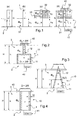
- the figure 1 represents for example a nanostructure, formed of a single nanofilament nanoconstituent.
- the nanowire in question is of cylindrical shape, and has a diameter D which is typically from a few tens to a few hundred nanometers, while its height H is of the order of one micron.
- the figure 7 represents a nanostructure formed of several nanoparticles nanoconstituents. It should be noted that in this type of nanostructure, it is obligatorily a plurality of nanoparticles. A nanoparticle is comparable to a sphere, whose typical diameter is a few tens to a few hundred nanometers.
- the invention can not be implemented for a structure having a single nanometric dimension. This limitation will be explained in more detail in the following description.
- the semiconductor device 10 illustrated on the figure 1 comprises nanostructure 1 of the nanowire type which has for example been obtained by growth on a substrate 2.
- the growth of the nanowire is for example carried out by MOCVD (for "Metal Organic Chemical Vapor Deposition" according to the English terminology).
- the substrate 2 may be made of sapphire Al 2 O 3. It may also comprise a layer of a few tens to a few hundred nanometers thick, for example zinc oxide ZnO deposited on the solid substrate of Al 2 O 3 . It can also be electrical conductor depending on the application considered.
- the nanostructure 1 After the growth step of the nanostructure 1, it is doped with n-type carriers (or p-type).
- the nanostructure is generally doped during growth (by adding a dopant to the precursor gas), but it can also be doped after growth by diffusion or ion implantation.
- the nanowire 1 has been coated with a dielectric element whose height h is less than the height H of the nanowire.
- the transverse upper face of the nanowire 1 is not coated, which makes it possible in particular to be able to subsequently deposit a metal contact at the upper end of the nanowire.
- the structure obtained at the end of these steps is for example represented on the figure 4 .
- the nanowire 1 having a cylindrical shape, has a transverse dimension comparable to a diameter D.
- the nanowire 1 is made of zinc oxide (ZnO) and the dielectric element chosen is a polymer 3 of the novolac resin type, for example the accuflo T-27 polymer from the company Honeywell.
- ZnO zinc oxide
- the dielectric element chosen is a polymer 3 of the novolac resin type, for example the accuflo T-27 polymer from the company Honeywell.
- this junction p-n is obtained very simply, with the only presence of a dielectric element coating the nanowire, in a single layer.
- the p-n junction obtained can be described as permanent insofar as there is no need to bias a metal layer to make the p-n junction.
- the principle illustrated experimentally above can be generalized to any type of coating material capable of forming a p-n junction inside the nanowire.
- a polymer or copolymer aromatic or otherwise, having conjugated ⁇ electron systems, for example polystyrene (aromatic ring C 6 H 6 ) and derivatives, polynaphthalene (aromatic ring C 10 H 8 ) and derivatives, polypropylene (aromatic ring C 16 H 10 ) and derivatives and / or electrophilic groups, for example halogenated.
- conjugated ⁇ electron systems for example polystyrene (aromatic ring C 6 H 6 ) and derivatives, polynaphthalene (aromatic ring C 10 H 8 ) and derivatives, polypropylene (aromatic ring C 16 H 10 ) and derivatives and / or electrophilic groups, for example halogenated.
- electrophilic materials are well adapted to generate a p-type inversion in the nanostructure, for example by hydrogenation of the surface of the semiconductor.
- the coating material is however not exclusively a polymeric material.
- inorganic materials such as oxides, for example SiO 2 .
- the coating material can be expanded to any type of dielectric material generating by its mere presence a suitable surface potential, that is to say, capable of reversing the conductivity type over a given width of the nanostructure.
- the principle illustrated experimentally above for a ZnO nanowire can also be generalized to any type of structure comprising a semiconductor material capable of forming a pn junction.
- the nanowire 1 can be made of Gallium Nitride (GaN), Aluminum Nitride (AlN), Indium Nitride (InN), Cadnium sulphide (CdS), Cadnium Selenide (CdSe) , Cadnium telluride (CdTe), Zinc sulphide (ZnS), Zinc selenide (ZnSe), Zinc telluride (ZnTe), Copium and Gallium diselenide (CuGaSe 2 ), Copper and Indium disulfide (CuInS 2 ), Copper and Indium Diselenide (CuInSe 2 ).
- This method allows the realization of a p-n junction in a nanostructure, as well as the realization of a nanostructure with a p-n junction to form a semiconductor device.
- the application considered is that of a nanostructure having at least one nanofilament-type nanoconstituent 1.
- the nanowire 1 has a height H, and, insofar as it has a cylindrical shape, the transverse dimension of the nanowire 1 corresponds to the diameter D thereof.
- step (b) a first dielectric element 31 of height h 1 is formed , encasing the nanowire 1 on this height h 1 , into a material generating a surface potential ⁇ s1 that is not suitable for inverting the type of conductivity of the nanowire thus coated.
- the height of the first dielectric element 31 may for example correspond to the half-height of the nanowire.
- Step (b) can be performed by centrifugation.
- an etching sub-step can be performed to precisely control the height h 1 of the deposition of the first dielectric element 31, and clean the surface of the uncoated nanowire 1.
- step (c) the first dielectric element 31 is covered with a second dielectric element 32 of height h 2 .
- the second dielectric element 32 thus coats the nanowire 1 on this height h 2 , a material generating a surface potential ⁇ s2 capable of reversing the conductivity type over the entire transverse dimension of the nanowire.
- the second dielectric element 32, and the first dielectric element 31 are in direct contact.
- the contact zone between the two dielectric elements 31, 32 is referenced 33.
- the second dielectric element 32 surrounds the cylindrical nanowire over its entire periphery. As a result, it is understood that it is sufficient to have a material capable of reversing the conductivity type on a transverse half-dimension of the nanowire 1, to finally reverse the conductivity type over the entire transverse dimension of the nanowire.
- the transverse half-dimension thus corresponds to the half-diameter (or radius) of the nanowire 1.
- width W of nanowire, taken along the transverse dimension of said nanowire, on which there is inversion of the conductivity type corresponds, at least, to the radius of the nanowire 1.
- the cumulative height h h 1 + h 2 of the dielectric elements 31, 32 encasing the nanowire 1 is smaller than the height H of the nanowire 1. This allows the subsequent deposition of a metal contact 42 on the nanowire 1.
- step (c) for example carried out by centrifugation, may be followed by a chemical-mechanical polishing step.
- the cumulative height h is also greater than the magnitude H-W so that the contacted end is in the inversion mode, otherwise the metal contact would not be in contact with the inversion zone.
- Centrifugation also known as "spin coating” in the English terminology
- spin coating consists in dispensing a dielectric in sol-gel form on the nanostructure, then in rotating the nanostructure in order to extend the dielectric on the nanostructure according to one controlled height, and finally to anneal to evaporate the solvents and form the solid dielectric.
- the sol-gel processes rely on a polymerization of molecular precursors in solution and allow the production of vitreous materials without resort to fusion.
- the chemical mechanical polishing allows a control of the height h 2 of the dielectric element 32. It should be noted that the dielectric element 32 and the nanowire 1 are polished at the same time, but their respective hardnesses being different, the result is a different topography.
- a pn junction was thus made in the nanowire 1 whose interface (also referred to as the junction plane) extends perpendicularly to the axis of the nanowire 1: speaks of axial pn junction.
- the axial p-n junction is formed by the sole presence of the dielectric material 32 around the nanowire 1, which induces, permanently, a reversal of the conductivity type in the nanowire 1.
- a step (d) of deposition of metal contacts 41, 42 is carried out on either side of the nanowire, each of the two contacts being adapted to the type of local conductivity of the nanowire, namely p or n.
- step (d) a semiconductor device having a nanostructure nanostructure 1 having a p-n junction was thus produced.
- Step (b) merely serves to provide electrical insulation around the p-n junction to be achieved, but is not essential for the formation of the p-n junction itself.
- step (b) can be envisaged.
- the figure 2 shows for example a nanostructure for which step (b) is not necessary.
- the application considered is that of a nanowire having two distinct parts 11, 12 with distinct transverse dimensions.
- the height of the nanowire 1 is denoted H.
- the two parts 11, 12 of the nanowire 1 in question are cylindrical, and have a common axis of symmetry.
- the transverse dimension of the first part 11 can therefore be likened to a diameter, denoted D 1 .
- the transverse half-dimension of the first portion 11 corresponds to the radius of this portion 11.
- the transverse dimension of the second portion 12 can also be likened to a diameter, denoted D 2 .
- the transverse half-dimension of the second portion 12 corresponds to the radius of this portion 12.
- step (c) is implemented.
- the height h of the dielectric element is such that it is greater than the magnitude H-W so that the end intended to receive a contact is in the inversion mode.
- step (c) for example carried out by centrifugation, may be followed by a chemical-mechanical polishing step to ensure that the height h of the dielectric element 3 is less than the height H of the nanowire 1.
- the deposition of a metal contact at the inversion zone can then be achieved.
- a semiconductor device made with a nanowire having a pn junction is obtained, by performing a step (d) of deposition of the metal contacts similar to that already presented on FIG. Figure 1 (d) .
- the pn junction obtained is axial insofar as a part of the interface of the junction extends perpendicular to the axis of the nanowire 1.
- the pn junction obtained is also radial insofar as another part of the interface of the junction extends parallel to the axis of the nanowire 1.
- the pn junction obtained being both axial and radial, it is called a hybrid or hybrid pn junction.
- junction p-n can improve the electrical transport and injection of electrons in the p-type portion to compensate for a density of charge carriers, that is to say, holes, lower in this part.
- the mixed p-n junction is thus formed by the sole presence of the dielectric material 3 around the nanowire 1, which induces, by its mere presence, a permanent inversion of the conductivity type in the nanowire 1.
- the figure 3 illustrates another variant embodiment of the invention.
- the application in question also relates to a nanowire 1 of conical shape.
- the nanowire 1 thus has a shape such that its transverse dimension D changes continuously with the height of the nanowire 1.
- the nanowire 1 illustrated on the figure 3 therefore does not have two distinct parts each having transverse dimensions D 1 , D 2 constants.
- the nanowire is conically shaped, a section made in a plane perpendicular to the axis of symmetry of the cone has the shape of a circle.
- the transverse half-dimension of the nanowire 1 to the dimension z corresponds to the radius of the nanowire 1 at this dimension.
- step (c) is implemented.
- the height h of the dielectric element 3 is smaller than the height H of the nanowire 1.
- the height h is also greater than the magnitude H-W.
- the conical shape ensures the presence of a small transverse dimension at one end of the nanowire 1 and consequently the existence of a part of a single type of conductivity (part 12) whatever the nature of the encapsulating material 3.
- a chemical mechanical polishing step can also be performed.
- a semiconductor device made with a nanowire 1 having a pn junction is obtained by performing a step (d) of deposition of the metal contacts similar to those of the embodiment variants illustrated in FIGS. Figures 1 or 2 .
- junction p-n thus produced is particularly advantageous for improving the extraction of light in the case of the embodiment of LED for example.
- junction p-n is achieved by the mere presence of the dielectric material 3 around the nanowire 1, which induces, by its mere presence, a permanent inversion of the conductivity type in the nanowire 1.
- the figure 4 also illustrates an alternative embodiment for which step (b) of the figure 1 is not necessary.
- the application considered is that of a cylindrical nanowire 1 thus having a constant transverse dimension over its entire height.
- the transverse dimension therefore corresponds to the diameter D of the cylinder formed by the nanowire 1.
- the transverse half-dimension then corresponds to the radius of the nanowire 1.
- step (c) makes it possible to lead to a pn junction in a nanowire 1, similar to that of the first part 11 of the nanowire 1 illustrated on FIG. figure 2 .
- step (c) here consists in inverting the conductivity type over a width (W) strictly smaller than the transverse half-dimension of the nanowire 1 (W ⁇ D / 2) over the entire height of said nanowire.
- step (c) for example carried out by centrifugation, may be followed by a chemical-mechanical polishing step to ensure that the height h of the dielectric element 3 is less than the height H of the nanowire 1.
- the height h is again greater than the magnitude HW.
- step (d) To produce the semiconductor device with a nanowire having a pn junction, it implements step (d).
- junction p-n can be described as radial. Indeed, the interface between the areas p and n extends parallel to the direction of the axis of symmetry of the nanowire.
- This nanostructure makes it possible, in particular, to increase the recombination surface of the carriers of each type, the interface between the two zones p and n being relatively large and consequently to increase the quantum yield of the nanostructure, the emission of photons being more important.
- the deposit of metallic contacts of this step (d) differs however from those provided for the pn junctions of Figures 1 to 3 .
- the metal contact 42 provided for the area p (n respectively) of the p-n junction must be annular and thin so as not to be in contact with the area n (p respectively) of the p-n junction of the nanowire 1.
- the radial p-n junction is formed by the sole presence of the dielectric material 3 around the nanowire 1, which induces, by its mere presence, a permanent inversion of the conductivity type in the nanowire 1.
- the figure 5 illustrates an embodiment variant of the invention similar to that illustrated on the figure 4 .
- the application considered is that of a nanowire 1 with a symmetrical shape of revolution and having a transverse dimension D varying continuously according to its height.
- the form is not conical.
- z represents a dimension along the axis of symmetry of the nanowire 1
- the transverse dimension of the nanowire 1 at this dimension z is then defined in a plane perpendicular to this axis of symmetry, as the diameter of the nanowire at this dimension.
- the transverse half-dimension of the nanowire 1 to the dimension z corresponds to the radius of the nanowire 1 at this dimension.
- step (c) is here repeated n times in succession, with n dielectric elements 31, 32,..., 3n each coating the nanowire 1 on a distinct part thereof and generating respectively a surface potential ⁇ S1 , ⁇ S2 , ..., ⁇ Sn distinct from each other.
- a chemical-mechanical polishing of the coating material 3n can be carried out.
- the cumulative height h h 1 + h 2 + ... + h n of the n enamelling materials 31, 32, ..., 3n is smaller than the height H of the nanowire and greater than the magnitude HW, where W represents the width inversion W n , for the subsequent deposition of the metal contact.
- step (d) is similar to that leading to the semiconductor device illustrated on FIG. figure 4 .
- junction p-n can be described as radial. Indeed, the interface between the zone p and the zone n extends parallel to the direction of the axis of symmetry of the nanowire.
- the nanostructure represented on the figure 5 allows to adjust the electrical transport and injection properties and the optical properties in the nanostructure, in order to improve the quantum yield (photon emission) and the extraction of these photons.
- step (a) it is possible to provide a step of producing Bragg mirrors, preferably during step (a).
- the p-n junction is made solely by the presence of the dielectric material 3 around the nanowire 1, which induces, by its mere presence, a permanent inversion of the conductivity type in the nanowire 1.
- the figure 6 illustrates an alternative embodiment of the invention also close to that illustrated on the figure 4 .
- the application considered is that of a nanowire 1 with a cylindrical shape, having a transverse dimension comparable to a diameter D.
- step (c) is here repeated three times in succession, with three dielectric elements 31, 32, 33 each coating the nanowire 1 on a distinct part thereof and generating respectively a surface potential ⁇ S1 , ⁇ S2 , ⁇ S3 distinct from each other.
- a chemical-mechanical polishing of the encapsulating material 33 can be carried out.
- the cumulative height h h 1 + h 2 + h 3 of the three embedding materials 31, 32, 33 is smaller than the height H of the nanowire and greater than the magnitude HW, where W represents the inversion width W 3 .
- step (d) is similar to that leading to the semiconductor device illustrated on FIG. figure 4 .
- the nanostructure represented on the figure 6 allows a good injection of the carriers in the zones n and p respectively, and offers a large recombination zone defined by the pn interface.
- the p-n junction is made solely by the presence of dielectric materials 32, 33 around the nanowire 1, which, by their very presence, induce a permanent inversion of the conductivity type in the nanowire 1.
- steps (c), (d) and optionally (b) apply at the same time to this plurality of nanowires.
- the figure 7 illustrates another variant embodiment of the invention, in which the nanostructure does not have one or more nanofilament (s) of the nanowire type, but a plurality of nanoparticle-type nanoconstituents.
- Each nanoparticle can be likened to a sphere of diameter D.
- the transverse dimension of a nanoparticle can therefore be defined by its diameter D.
- the transverse half-dimension of this nanoparticle can be likened to the radius of the nanoparticle.
- the nanostructure is formed of a plurality of nanoparticle-type nanoconstituents, exhibiting properties of quantum confinement.
- Quantum confinement means that the displacement of electrons or holes is limited in at least one direction. This property is related to the size of the nanoparticles compared to the Bohr radius.
- the nanoparticles are in contact with each other, so as to ensure electrical contact.
- nanoparticles can be formed by different methods. Indeed, it is conceivable to use a process derived from the PLD method (for "Pulsed Laser Deposition” according to the English terminology), a laser pyrolysis method or chemical methods ( ML Kahn et al., Adv. Func. Mater. 2005, 15, 458 ).
- the method for producing a pn junction in such a nanostructure and the method for producing a semiconductor device associated with this nanostructure, repeat the steps (b), (c) and (d) illustrated in FIG. figure 1 .
- a first dielectric element 31 of height h 1 is formed , coating the plurality of nanoparticles on a first portion of the height nanostructure h 1 , into a material generating a surface potential ⁇ s1 not able to reverse the conductivity type of the nanoparticles included in this first part.
- a step (c) covering the first dielectric element 31 with a second dielectric element 32 of height h 2 .
- the second dielectric element 32 thus surrounds a second part of the nanostructure on this height h 2 , in a material generating a surface potential ⁇ s2 capable of reversing the conductivity type over the entire transverse dimension of the nanoparticles included in this second part.
- the inversion of the conductivity type in the nanowire 1 is permanent and obtained by the mere presence of the dielectric element coating the nanoparticles.
- the two parts of the nanostructure are in direct contact at a contact plane 33.
- Step (c) may for example be performed by centrifugation, and may be followed by a chemical mechanical polishing step.
- step (d) is carried out in a manner analogous to that illustrated in FIG. figure 2 to realize the semiconductor device.
- these processes can only be applied to nanostructures having one or more nanoconstituents with at least two nanometric dimensions.
- the figure 8 represents a theoretical calculation providing the evolution of the potential 21 according to a transverse dimension (diameter D) of a nanowire 1 to which a surface potential ⁇ S is applied.
- the potential within the nanowire 1 decreases very slowly over a width W of the nanowire, this width being defined in the transverse direction of the nanowire (W ⁇ D).
- This width W corresponds to the nanowire width on which there is a reversal of the conductivity type.
- the width over which the conductivity type is reversed is 8 to 10 times greater for a nanowire than for a plane structure, all things being equal.
- the nanostructures considered in the context of the invention allow it.
- the choice of a suitable dielectric embedding material and / or, according to the embodiment, a suitable transverse dimension of the nanoconstituent allows (tent) to determine the width of the nanoconstituent on which it is desired to perform an inversion the type of conductivity.
- Another way of defining the application condition of the invention is to specify that the invention can be implemented only for nanostructures having one or more nanoconstituent (s) with a high surface area / volume ratio.
- the inversion width W is a dimension extending in the direction of the transverse dimension of the nanoconstituent considered.
Applications Claiming Priority (1)
| Application Number | Priority Date | Filing Date | Title |
|---|---|---|---|
| FR0900270A FR2941325B1 (fr) | 2009-01-22 | 2009-01-22 | Procede de realisation d'une homojonction pn dans une nanostructure |
Publications (3)
| Publication Number | Publication Date |
|---|---|
| EP2211387A2 true EP2211387A2 (de) | 2010-07-28 |
| EP2211387A3 EP2211387A3 (de) | 2011-03-30 |
| EP2211387B1 EP2211387B1 (de) | 2013-07-10 |
Family
ID=41078114
Family Applications (1)
| Application Number | Title | Priority Date | Filing Date |
|---|---|---|---|
| EP10290025.5A Not-in-force EP2211387B1 (de) | 2009-01-22 | 2010-01-19 | Verfahren zur Herstellung eines homogenen pn-Übergangs in einer Nanostruktur |
Country Status (4)
| Country | Link |
|---|---|
| US (1) | US8178431B2 (de) |
| EP (1) | EP2211387B1 (de) |
| JP (1) | JP5553620B2 (de) |
| FR (1) | FR2941325B1 (de) |
Cited By (13)
| Publication number | Priority date | Publication date | Assignee | Title |
|---|---|---|---|---|
| US11201265B2 (en) | 2018-09-27 | 2021-12-14 | Lumileds Llc | Micro light emitting devices |
| US11569415B2 (en) | 2020-03-11 | 2023-01-31 | Lumileds Llc | Light emitting diode devices with defined hard mask opening |
| US11600656B2 (en) | 2020-12-14 | 2023-03-07 | Lumileds Llc | Light emitting diode device |
| US11626538B2 (en) | 2020-10-29 | 2023-04-11 | Lumileds Llc | Light emitting diode device with tunable emission |
| US11705534B2 (en) | 2020-12-01 | 2023-07-18 | Lumileds Llc | Methods of making flip chip micro light emitting diodes |
| US11735695B2 (en) | 2020-03-11 | 2023-08-22 | Lumileds Llc | Light emitting diode devices with current spreading layer |
| US11777059B2 (en) | 2019-11-20 | 2023-10-03 | Lumileds Llc | Pixelated light-emitting diode for self-aligned photoresist patterning |
| US11848402B2 (en) | 2020-03-11 | 2023-12-19 | Lumileds Llc | Light emitting diode devices with multilayer composite film including current spreading layer |
| US11901491B2 (en) | 2020-10-29 | 2024-02-13 | Lumileds Llc | Light emitting diode devices |
| US11935987B2 (en) | 2021-11-03 | 2024-03-19 | Lumileds Llc | Light emitting diode arrays with a light-emitting pixel area |
| US11942507B2 (en) | 2020-03-11 | 2024-03-26 | Lumileds Llc | Light emitting diode devices |
| US11955583B2 (en) | 2020-12-01 | 2024-04-09 | Lumileds Llc | Flip chip micro light emitting diodes |
| US11961875B2 (en) | 2023-01-19 | 2024-04-16 | Lumileds Llc | Monolithic segmented LED array architecture with islanded epitaxial growth |
Families Citing this family (2)
| Publication number | Priority date | Publication date | Assignee | Title |
|---|---|---|---|---|
| US8389387B2 (en) * | 2009-01-06 | 2013-03-05 | Brookhaven Science Associates, Llc | Segmented nanowires displaying locally controllable properties |
| WO2012067687A2 (en) * | 2010-08-26 | 2012-05-24 | The Ohio State University | Nanoscale emitters with polarization grading |
Citations (1)
| Publication number | Priority date | Publication date | Assignee | Title |
|---|---|---|---|---|
| WO2004088755A1 (en) | 2003-04-04 | 2004-10-14 | Startskottet 22286 Ab | Nanowhiskers with pn junctions and methods of fabricating thereof |
Family Cites Families (3)
| Publication number | Priority date | Publication date | Assignee | Title |
|---|---|---|---|---|
| KR100552707B1 (ko) * | 2004-04-07 | 2006-02-20 | 삼성전자주식회사 | 나노와이어 발광소자 및 그 제조방법 |
| US7692179B2 (en) * | 2004-07-09 | 2010-04-06 | Hewlett-Packard Development Company, L.P. | Nanowire device with (111) vertical sidewalls and method of fabrication |
| US7202173B2 (en) * | 2004-12-20 | 2007-04-10 | Palo Alto Research Corporation Incorporated | Systems and methods for electrical contacts to arrays of vertically aligned nanorods |
-
2009
- 2009-01-22 FR FR0900270A patent/FR2941325B1/fr not_active Expired - Fee Related
-
2010
- 2010-01-18 JP JP2010007929A patent/JP5553620B2/ja not_active Expired - Fee Related
- 2010-01-19 EP EP10290025.5A patent/EP2211387B1/de not_active Not-in-force
- 2010-01-22 US US12/691,925 patent/US8178431B2/en active Active
Patent Citations (1)
| Publication number | Priority date | Publication date | Assignee | Title |
|---|---|---|---|---|
| WO2004088755A1 (en) | 2003-04-04 | 2004-10-14 | Startskottet 22286 Ab | Nanowhiskers with pn junctions and methods of fabricating thereof |
Non-Patent Citations (3)
| Title |
|---|
| GC. YI; C. WANG; WI. PARK, SEMICONDUCTOR SCIENCE AND TECHNOLOGY, vol. 20, 10520, pages S22 - S34 |
| M. L. KAHN ET AL., ADV. FUNC. MATER., vol. 15, 10520, pages 458 |
| Z.L. WANG, MATERIALSTODAY, 6260420 |
Cited By (18)
| Publication number | Priority date | Publication date | Assignee | Title |
|---|---|---|---|---|
| US11271033B2 (en) | 2018-09-27 | 2022-03-08 | Lumileds Llc | Micro light emitting devices |
| US11735691B2 (en) | 2018-09-27 | 2023-08-22 | Lumileds Llc | Micro light emitting devices |
| US11201265B2 (en) | 2018-09-27 | 2021-12-14 | Lumileds Llc | Micro light emitting devices |
| US11777059B2 (en) | 2019-11-20 | 2023-10-03 | Lumileds Llc | Pixelated light-emitting diode for self-aligned photoresist patterning |
| US11569415B2 (en) | 2020-03-11 | 2023-01-31 | Lumileds Llc | Light emitting diode devices with defined hard mask opening |
| US11942507B2 (en) | 2020-03-11 | 2024-03-26 | Lumileds Llc | Light emitting diode devices |
| US11848402B2 (en) | 2020-03-11 | 2023-12-19 | Lumileds Llc | Light emitting diode devices with multilayer composite film including current spreading layer |
| US11784286B2 (en) | 2020-03-11 | 2023-10-10 | Lumileds Llc | Light emitting diode devices with defined hard mask opening |
| US11735695B2 (en) | 2020-03-11 | 2023-08-22 | Lumileds Llc | Light emitting diode devices with current spreading layer |
| US11777061B2 (en) | 2020-10-29 | 2023-10-03 | Lumileds Llc | Light emitting diode device with tunable emission |
| US11626538B2 (en) | 2020-10-29 | 2023-04-11 | Lumileds Llc | Light emitting diode device with tunable emission |
| US11901491B2 (en) | 2020-10-29 | 2024-02-13 | Lumileds Llc | Light emitting diode devices |
| US11705534B2 (en) | 2020-12-01 | 2023-07-18 | Lumileds Llc | Methods of making flip chip micro light emitting diodes |
| US11955583B2 (en) | 2020-12-01 | 2024-04-09 | Lumileds Llc | Flip chip micro light emitting diodes |
| US11923402B2 (en) | 2020-12-14 | 2024-03-05 | Lumileds Llc | Light emitting diode device |
| US11600656B2 (en) | 2020-12-14 | 2023-03-07 | Lumileds Llc | Light emitting diode device |
| US11935987B2 (en) | 2021-11-03 | 2024-03-19 | Lumileds Llc | Light emitting diode arrays with a light-emitting pixel area |
| US11961875B2 (en) | 2023-01-19 | 2024-04-16 | Lumileds Llc | Monolithic segmented LED array architecture with islanded epitaxial growth |
Also Published As
| Publication number | Publication date |
|---|---|
| US20100193766A1 (en) | 2010-08-05 |
| FR2941325B1 (fr) | 2011-04-22 |
| JP2010171425A (ja) | 2010-08-05 |
| EP2211387A3 (de) | 2011-03-30 |
| US8178431B2 (en) | 2012-05-15 |
| JP5553620B2 (ja) | 2014-07-16 |
| EP2211387B1 (de) | 2013-07-10 |
| FR2941325A1 (fr) | 2010-07-23 |
Similar Documents
| Publication | Publication Date | Title |
|---|---|---|
| EP2211387B1 (de) | Verfahren zur Herstellung eines homogenen pn-Übergangs in einer Nanostruktur | |
| EP2715808B1 (de) | Halbleiterstruktur zur ausstrahlung von licht und verfahren zur herstellung einer solchen struktur | |
| EP2203939B1 (de) | Optoelektronische anordnung mit nanodrähten und entsprechende verfahren | |
| FR2923651A1 (fr) | Procede de realisation d'une jonction pn dans un nanofil, et d'un nanofil avec au moins une jonction pn. | |
| EP0606453A1 (de) | Photovoltaische zelle. | |
| WO2006097591A1 (fr) | Procede de fabrication d’une diode electroluminescente a jonction pn nanostructuree et diode obtenue par un tel procede | |
| EP2795685A1 (de) | Verfahren zur herstellung eines halbleitermikro- oder nanodrahtes, halbleiterstruktur mit einem solchen mikro- oder nanodraht und verfahren zum herstellen einer halbleiterstruktur | |
| FR2967813A1 (fr) | Procédé de réalisation d'une structure a couche métallique enterrée | |
| FR2964498A1 (fr) | Empilement de led de couleur | |
| FR3027452A1 (fr) | Procede de fabrication d'une photodiode a faible bruit | |
| FR3105567A1 (fr) | Procede pour fabriquer une structure gan/ingan relaxee | |
| EP3815143B1 (de) | Verfahren zur herstellung einer optoelektronischen vorrichtung mit selbstausgerichteten lichtbegrenzenden wänden | |
| EP2697833A2 (de) | Halbleiterheterostruktur und fotovoltaikzelle mit einer solchen heterostruktur | |
| EP2800151B1 (de) | Optoelektronische Anordnung, die mit einem Halbleiter-Nanodraht ausgestattet ist, dessen Längsabschnitt von einem Spiegelteil umgeben ist | |
| EP0229574A1 (de) | Photovoltaischer HgCdTe-Heteroübergang-Detektor und Verfahren zu seiner Herstellung | |
| WO2013102664A1 (fr) | Substrat structure pour leds a forte extraction de lumiere | |
| EP3740974B1 (de) | Optoelektronische vorrichtung umfassend ein gitter und eine kathode gekoppelt miteinander | |
| FR2839204A1 (fr) | Dispositif metal-oxyde-silicium comprenant une structure d'oxyde a l'echelle du nanometre. | |
| EP3602640A1 (de) | Nanodrahtstruktur und verfahren zur herstellung solch einer struktur | |
| FR2965975A1 (fr) | Transistor a effet de champ sur ilot de matériau semi-conducteur auto-assemble | |
| EP2747155A1 (de) | Herstellungsverfahren für eine Struktur des Typs MIS, im besonderen für eine Leuchtdiode | |
| FR2994766A1 (fr) | Procede de transfert d'un film d'inp | |
| EP4082049A1 (de) | Diode mit mindestens zwei passivierungsschichten, insbesondere aus dielektrika, die zur optimierung der passivierung lokal gestapelt sind | |
| FR3123758A1 (fr) | Procede pour fabriquer un substrat comprenant une couche d’ingan relaxee et substrat ainsi obtenu pour la reprise de croissance d’une structure led | |
| FR3001335A1 (fr) | Structure semiconductrice et procede de fabrication d'une structure semiconductrice |
Legal Events
| Date | Code | Title | Description |
|---|---|---|---|
| PUAI | Public reference made under article 153(3) epc to a published international application that has entered the european phase |
Free format text: ORIGINAL CODE: 0009012 |
|
| AK | Designated contracting states |
Kind code of ref document: A2 Designated state(s): AT BE BG CH CY CZ DE DK EE ES FI FR GB GR HR HU IE IS IT LI LT LU LV MC MK MT NL NO PL PT RO SE SI SK SM TR |
|
| AX | Request for extension of the european patent |
Extension state: AL BA RS |
|
| RIN1 | Information on inventor provided before grant (corrected) |
Inventor name: GILET, PHILIPPE Inventor name: ROMAIN-LATU, EDDY |
|
| PUAL | Search report despatched |
Free format text: ORIGINAL CODE: 0009013 |
|
| AK | Designated contracting states |
Kind code of ref document: A3 Designated state(s): AT BE BG CH CY CZ DE DK EE ES FI FR GB GR HR HU IE IS IT LI LT LU LV MC MK MT NL NO PL PT RO SE SI SK SM TR |
|
| AX | Request for extension of the european patent |
Extension state: AL BA RS |
|
| 17P | Request for examination filed |
Effective date: 20110426 |
|
| 17Q | First examination report despatched |
Effective date: 20120716 |
|
| GRAP | Despatch of communication of intention to grant a patent |
Free format text: ORIGINAL CODE: EPIDOSNIGR1 |
|
| RIC1 | Information provided on ipc code assigned before grant |
Ipc: H01L 33/02 20100101ALI20130207BHEP Ipc: H01L 29/24 20060101ALN20130207BHEP Ipc: H01L 33/18 20100101ALI20130207BHEP Ipc: H01L 29/861 20060101AFI20130207BHEP Ipc: H01L 29/06 20060101ALI20130207BHEP Ipc: H01L 29/20 20060101ALN20130207BHEP Ipc: H01L 21/329 20060101ALI20130207BHEP Ipc: H01L 33/28 20100101ALN20130207BHEP |
|
| RIC1 | Information provided on ipc code assigned before grant |
Ipc: H01L 21/329 20060101ALI20130211BHEP Ipc: H01L 29/06 20060101ALI20130211BHEP Ipc: H01L 29/20 20060101ALN20130211BHEP Ipc: H01L 33/28 20100101ALN20130211BHEP Ipc: H01L 33/02 20100101ALI20130211BHEP Ipc: H01L 29/861 20060101AFI20130211BHEP Ipc: H01L 33/18 20100101ALI20130211BHEP Ipc: H01L 29/24 20060101ALN20130211BHEP |
|
| GRAS | Grant fee paid |
Free format text: ORIGINAL CODE: EPIDOSNIGR3 |
|
| GRAA | (expected) grant |
Free format text: ORIGINAL CODE: 0009210 |
|
| AK | Designated contracting states |
Kind code of ref document: B1 Designated state(s): AT BE BG CH CY CZ DE DK EE ES FI FR GB GR HR HU IE IS IT LI LT LU LV MC MK MT NL NO PL PT RO SE SI SK SM TR |
|
| REG | Reference to a national code |
Ref country code: GB Ref legal event code: FG4D Free format text: NOT ENGLISH |
|
| REG | Reference to a national code |
Ref country code: AT Ref legal event code: REF Ref document number: 621392 Country of ref document: AT Kind code of ref document: T Effective date: 20130715 Ref country code: CH Ref legal event code: EP |
|
| REG | Reference to a national code |
Ref country code: IE Ref legal event code: FG4D Free format text: LANGUAGE OF EP DOCUMENT: FRENCH |
|
| REG | Reference to a national code |
Ref country code: DE Ref legal event code: R096 Ref document number: 602010008392 Country of ref document: DE Effective date: 20130905 |
|
| REG | Reference to a national code |
Ref country code: SE Ref legal event code: TRGR |
|
| PG25 | Lapsed in a contracting state [announced via postgrant information from national office to epo] |
Ref country code: SI Free format text: LAPSE BECAUSE OF FAILURE TO SUBMIT A TRANSLATION OF THE DESCRIPTION OR TO PAY THE FEE WITHIN THE PRESCRIBED TIME-LIMIT Effective date: 20130710 |
|
| REG | Reference to a national code |
Ref country code: AT Ref legal event code: MK05 Ref document number: 621392 Country of ref document: AT Kind code of ref document: T Effective date: 20130710 |
|
| REG | Reference to a national code |
Ref country code: NL Ref legal event code: VDEP Effective date: 20130710 |
|
| REG | Reference to a national code |
Ref country code: LT Ref legal event code: MG4D |
|
| PG25 | Lapsed in a contracting state [announced via postgrant information from national office to epo] |
Ref country code: PT Free format text: LAPSE BECAUSE OF FAILURE TO SUBMIT A TRANSLATION OF THE DESCRIPTION OR TO PAY THE FEE WITHIN THE PRESCRIBED TIME-LIMIT Effective date: 20131111 Ref country code: HR Free format text: LAPSE BECAUSE OF FAILURE TO SUBMIT A TRANSLATION OF THE DESCRIPTION OR TO PAY THE FEE WITHIN THE PRESCRIBED TIME-LIMIT Effective date: 20130710 Ref country code: AT Free format text: LAPSE BECAUSE OF FAILURE TO SUBMIT A TRANSLATION OF THE DESCRIPTION OR TO PAY THE FEE WITHIN THE PRESCRIBED TIME-LIMIT Effective date: 20130710 Ref country code: CY Free format text: LAPSE BECAUSE OF FAILURE TO SUBMIT A TRANSLATION OF THE DESCRIPTION OR TO PAY THE FEE WITHIN THE PRESCRIBED TIME-LIMIT Effective date: 20130904 Ref country code: NO Free format text: LAPSE BECAUSE OF FAILURE TO SUBMIT A TRANSLATION OF THE DESCRIPTION OR TO PAY THE FEE WITHIN THE PRESCRIBED TIME-LIMIT Effective date: 20131010 Ref country code: LT Free format text: LAPSE BECAUSE OF FAILURE TO SUBMIT A TRANSLATION OF THE DESCRIPTION OR TO PAY THE FEE WITHIN THE PRESCRIBED TIME-LIMIT Effective date: 20130710 Ref country code: IS Free format text: LAPSE BECAUSE OF FAILURE TO SUBMIT A TRANSLATION OF THE DESCRIPTION OR TO PAY THE FEE WITHIN THE PRESCRIBED TIME-LIMIT Effective date: 20131110 |
|
| PG25 | Lapsed in a contracting state [announced via postgrant information from national office to epo] |
Ref country code: ES Free format text: LAPSE BECAUSE OF FAILURE TO SUBMIT A TRANSLATION OF THE DESCRIPTION OR TO PAY THE FEE WITHIN THE PRESCRIBED TIME-LIMIT Effective date: 20131021 Ref country code: NL Free format text: LAPSE BECAUSE OF FAILURE TO SUBMIT A TRANSLATION OF THE DESCRIPTION OR TO PAY THE FEE WITHIN THE PRESCRIBED TIME-LIMIT Effective date: 20130710 Ref country code: FI Free format text: LAPSE BECAUSE OF FAILURE TO SUBMIT A TRANSLATION OF THE DESCRIPTION OR TO PAY THE FEE WITHIN THE PRESCRIBED TIME-LIMIT Effective date: 20130710 Ref country code: PL Free format text: LAPSE BECAUSE OF FAILURE TO SUBMIT A TRANSLATION OF THE DESCRIPTION OR TO PAY THE FEE WITHIN THE PRESCRIBED TIME-LIMIT Effective date: 20130710 Ref country code: GR Free format text: LAPSE BECAUSE OF FAILURE TO SUBMIT A TRANSLATION OF THE DESCRIPTION OR TO PAY THE FEE WITHIN THE PRESCRIBED TIME-LIMIT Effective date: 20131011 Ref country code: LV Free format text: LAPSE BECAUSE OF FAILURE TO SUBMIT A TRANSLATION OF THE DESCRIPTION OR TO PAY THE FEE WITHIN THE PRESCRIBED TIME-LIMIT Effective date: 20130710 |
|
| PG25 | Lapsed in a contracting state [announced via postgrant information from national office to epo] |
Ref country code: CY Free format text: LAPSE BECAUSE OF FAILURE TO SUBMIT A TRANSLATION OF THE DESCRIPTION OR TO PAY THE FEE WITHIN THE PRESCRIBED TIME-LIMIT Effective date: 20130710 |
|
| PG25 | Lapsed in a contracting state [announced via postgrant information from national office to epo] |
Ref country code: DK Free format text: LAPSE BECAUSE OF FAILURE TO SUBMIT A TRANSLATION OF THE DESCRIPTION OR TO PAY THE FEE WITHIN THE PRESCRIBED TIME-LIMIT Effective date: 20130710 Ref country code: EE Free format text: LAPSE BECAUSE OF FAILURE TO SUBMIT A TRANSLATION OF THE DESCRIPTION OR TO PAY THE FEE WITHIN THE PRESCRIBED TIME-LIMIT Effective date: 20130710 Ref country code: RO Free format text: LAPSE BECAUSE OF FAILURE TO SUBMIT A TRANSLATION OF THE DESCRIPTION OR TO PAY THE FEE WITHIN THE PRESCRIBED TIME-LIMIT Effective date: 20130710 Ref country code: CZ Free format text: LAPSE BECAUSE OF FAILURE TO SUBMIT A TRANSLATION OF THE DESCRIPTION OR TO PAY THE FEE WITHIN THE PRESCRIBED TIME-LIMIT Effective date: 20130710 Ref country code: SK Free format text: LAPSE BECAUSE OF FAILURE TO SUBMIT A TRANSLATION OF THE DESCRIPTION OR TO PAY THE FEE WITHIN THE PRESCRIBED TIME-LIMIT Effective date: 20130710 |
|
| PLBE | No opposition filed within time limit |
Free format text: ORIGINAL CODE: 0009261 |
|
| STAA | Information on the status of an ep patent application or granted ep patent |
Free format text: STATUS: NO OPPOSITION FILED WITHIN TIME LIMIT |
|
| 26N | No opposition filed |
Effective date: 20140411 |
|
| REG | Reference to a national code |
Ref country code: DE Ref legal event code: R097 Ref document number: 602010008392 Country of ref document: DE Effective date: 20140411 |
|
| BERE | Be: lapsed |
Owner name: COMMISSARIAT A L'ENERGIE ATOMIQUE ET AUX ENERGIES Effective date: 20140131 |
|
| PG25 | Lapsed in a contracting state [announced via postgrant information from national office to epo] |
Ref country code: LU Free format text: LAPSE BECAUSE OF FAILURE TO SUBMIT A TRANSLATION OF THE DESCRIPTION OR TO PAY THE FEE WITHIN THE PRESCRIBED TIME-LIMIT Effective date: 20140119 Ref country code: MC Free format text: LAPSE BECAUSE OF FAILURE TO SUBMIT A TRANSLATION OF THE DESCRIPTION OR TO PAY THE FEE WITHIN THE PRESCRIBED TIME-LIMIT Effective date: 20130710 |
|
| REG | Reference to a national code |
Ref country code: CH Ref legal event code: PL |
|
| PG25 | Lapsed in a contracting state [announced via postgrant information from national office to epo] |
Ref country code: LI Free format text: LAPSE BECAUSE OF NON-PAYMENT OF DUE FEES Effective date: 20140131 Ref country code: CH Free format text: LAPSE BECAUSE OF NON-PAYMENT OF DUE FEES Effective date: 20140131 |
|
| REG | Reference to a national code |
Ref country code: IE Ref legal event code: MM4A |
|
| PG25 | Lapsed in a contracting state [announced via postgrant information from national office to epo] |
Ref country code: BE Free format text: LAPSE BECAUSE OF NON-PAYMENT OF DUE FEES Effective date: 20140131 Ref country code: IE Free format text: LAPSE BECAUSE OF NON-PAYMENT OF DUE FEES Effective date: 20140119 |
|
| REG | Reference to a national code |
Ref country code: FR Ref legal event code: PLFP Year of fee payment: 6 |
|
| REG | Reference to a national code |
Ref country code: FR Ref legal event code: PLFP Year of fee payment: 7 |
|
| PG25 | Lapsed in a contracting state [announced via postgrant information from national office to epo] |
Ref country code: MT Free format text: LAPSE BECAUSE OF FAILURE TO SUBMIT A TRANSLATION OF THE DESCRIPTION OR TO PAY THE FEE WITHIN THE PRESCRIBED TIME-LIMIT Effective date: 20130710 |
|
| PG25 | Lapsed in a contracting state [announced via postgrant information from national office to epo] |
Ref country code: SM Free format text: LAPSE BECAUSE OF FAILURE TO SUBMIT A TRANSLATION OF THE DESCRIPTION OR TO PAY THE FEE WITHIN THE PRESCRIBED TIME-LIMIT Effective date: 20130710 |
|
| PG25 | Lapsed in a contracting state [announced via postgrant information from national office to epo] |
Ref country code: BG Free format text: LAPSE BECAUSE OF FAILURE TO SUBMIT A TRANSLATION OF THE DESCRIPTION OR TO PAY THE FEE WITHIN THE PRESCRIBED TIME-LIMIT Effective date: 20130710 |
|
| PG25 | Lapsed in a contracting state [announced via postgrant information from national office to epo] |
Ref country code: HU Free format text: LAPSE BECAUSE OF FAILURE TO SUBMIT A TRANSLATION OF THE DESCRIPTION OR TO PAY THE FEE WITHIN THE PRESCRIBED TIME-LIMIT; INVALID AB INITIO Effective date: 20100119 Ref country code: TR Free format text: LAPSE BECAUSE OF FAILURE TO SUBMIT A TRANSLATION OF THE DESCRIPTION OR TO PAY THE FEE WITHIN THE PRESCRIBED TIME-LIMIT Effective date: 20130710 |
|
| REG | Reference to a national code |
Ref country code: FR Ref legal event code: PLFP Year of fee payment: 8 |
|
| REG | Reference to a national code |
Ref country code: FR Ref legal event code: PLFP Year of fee payment: 9 |
|
| PG25 | Lapsed in a contracting state [announced via postgrant information from national office to epo] |
Ref country code: MK Free format text: LAPSE BECAUSE OF FAILURE TO SUBMIT A TRANSLATION OF THE DESCRIPTION OR TO PAY THE FEE WITHIN THE PRESCRIBED TIME-LIMIT Effective date: 20130710 |
|
| PGFP | Annual fee paid to national office [announced via postgrant information from national office to epo] |
Ref country code: SE Payment date: 20200115 Year of fee payment: 11 Ref country code: GB Payment date: 20200131 Year of fee payment: 11 Ref country code: DE Payment date: 20200113 Year of fee payment: 11 Ref country code: IT Payment date: 20200113 Year of fee payment: 11 |
|
| PGFP | Annual fee paid to national office [announced via postgrant information from national office to epo] |
Ref country code: FR Payment date: 20200130 Year of fee payment: 11 |
|
| REG | Reference to a national code |
Ref country code: DE Ref legal event code: R119 Ref document number: 602010008392 Country of ref document: DE |
|
| REG | Reference to a national code |
Ref country code: SE Ref legal event code: EUG |
|
| GBPC | Gb: european patent ceased through non-payment of renewal fee |
Effective date: 20210119 |
|
| PG25 | Lapsed in a contracting state [announced via postgrant information from national office to epo] |
Ref country code: FR Free format text: LAPSE BECAUSE OF NON-PAYMENT OF DUE FEES Effective date: 20210131 |
|
| PG25 | Lapsed in a contracting state [announced via postgrant information from national office to epo] |
Ref country code: SE Free format text: LAPSE BECAUSE OF NON-PAYMENT OF DUE FEES Effective date: 20210120 Ref country code: DE Free format text: LAPSE BECAUSE OF NON-PAYMENT OF DUE FEES Effective date: 20210803 Ref country code: GB Free format text: LAPSE BECAUSE OF NON-PAYMENT OF DUE FEES Effective date: 20210119 |
|
| PG25 | Lapsed in a contracting state [announced via postgrant information from national office to epo] |
Ref country code: IT Free format text: LAPSE BECAUSE OF NON-PAYMENT OF DUE FEES Effective date: 20210119 |