EP2211304A2 - Bildverarbeitungsvorrichtung - Google Patents
Bildverarbeitungsvorrichtung Download PDFInfo
- Publication number
- EP2211304A2 EP2211304A2 EP10000479A EP10000479A EP2211304A2 EP 2211304 A2 EP2211304 A2 EP 2211304A2 EP 10000479 A EP10000479 A EP 10000479A EP 10000479 A EP10000479 A EP 10000479A EP 2211304 A2 EP2211304 A2 EP 2211304A2
- Authority
- EP
- European Patent Office
- Prior art keywords
- zoom
- image
- interpolated
- pixel
- pixels
- Prior art date
- Legal status (The legal status is an assumption and is not a legal conclusion. Google has not performed a legal analysis and makes no representation as to the accuracy of the status listed.)
- Withdrawn
Links
Images






Classifications
-
- G—PHYSICS
- G06—COMPUTING OR CALCULATING; COUNTING
- G06T—IMAGE DATA PROCESSING OR GENERATION, IN GENERAL
- G06T3/00—Geometric image transformations in the plane of the image
- G06T3/40—Scaling of whole images or parts thereof, e.g. expanding or contracting
- G06T3/4015—Image demosaicing, e.g. colour filter arrays [CFA] or Bayer patterns
-
- H—ELECTRICITY
- H04—ELECTRIC COMMUNICATION TECHNIQUE
- H04N—PICTORIAL COMMUNICATION, e.g. TELEVISION
- H04N9/00—Details of colour television systems
- H04N9/64—Circuits for processing colour signals
Definitions
- the present invention relates to an image processing apparatus. More particularly, the present invention relates to an image processing apparatus which creates a zoom image having a desired zoom magnification based on an original image in which a plurality of pixels, each of which has any one of a plurality of colors, are arrayed in a predetermined manner.
- a scaling parameter corresponding to an electronic zoom magnification instructed by a zoom key is set to a RAW data-use scaling circuit
- the RAW data-use scaling circuit performs a scaling process (zoom process) that is with reference to the scaling parameter, on RAW data outputted from an A/D converter.
- the RAW data on which the scaling process is performed is recorded on a recording medium in a compressed state.
- the data on which the scaling process is performed is the RAW data, and thus, each of a plurality of pixels has only any one of color information, i.e., R(Red), G(Green), and B(Blue).
- the RAW data corresponds to a Bayer array of primary colors, and thus, colors of the adjacent two pixels differ from each other both in a vertical direction and a horizontal direction.
- the scaling process is a process for weighting the color information of such pixels and adding the results. Therefore, in the above-described apparatus, it is probable that the quality of the RAW data on which the scaling process is performed is deteriorated.
- a primary object of the present invention is to provide an image processing apparatus capable of improving the quality of an image on which a zoom process is performed.
- An image processing apparatus comprises: a fetcher which fetches an original image in which a plurality of original pixels, each of which has any one of M (M: an integer of 3 or more) colors, are arrayed in a predetermined manner, an interpolated image creator which performs a color interpolating process on the original image fetched by the fetcher so as to create an interpolated image formed by a plurality of interpolated pixels, each of which has N (N: an integer of 2 or more and less than the M) colors; and a zoom image creator which performs a zoom process on the interpolated image created by the interpolated image creator so as to create a zoom image in which a plurality of zoom pixels, each of which has any one of the M colors, are arrayed in the predetermined manner.
- M an integer of 3 or more
- the fetcher fetches original image in which a plurality of original pixels, each of which has any one of M (M: an integer of 3 or more) colors, are arrayed in a predetermined manner.
- the interpolated image creator performs a color interpolating process on the original image fetched by the fetcher so as to create an interpolated image formed by a plurality of interpolated pixels, each of which has N (N: an integer of 2 or more and less than the M) colors.
- the zoom image creator performs a zoom process on the interpolated image created by the interpolated image creator so as to create a zoom image in which a plurality of zoom pixels, each of which has any one of the M colors, are arrayed in the predetermined manner.
- the interpolated image is created by the color interpolating process for the original image, the interpolated image has more color information than the original image.
- the zoom image is created by the zoom process for such an interpolated image. Thereby, the quality of the zoom image is improved
- the zoom image has the same color array as that of the original image, and each pixel forming the interpolated image has one portion of the colors.
- the interpolated image is created by the color interpolating process for the original image, and the zoom image is created by the zoom process for the interpolated image. Thereby, it becomes possible to inhibit a circuit scale.
- an array of the predetermined manner includes a first partial array to which a first original pixel column intermittently having original pixels of a first color and a second pixel column intermittently having original pixels of a second color are allocated in a predetermined order
- the interpolated pixel creator includes a first interpolated-image creator which creates a first interpolated image to which a first interpolated-pixel column continuously having interpolated pixels of the first color and a second interpolated-pixel column continuously having interpolated pixels of the second color are allocated in the predetermined order, based on the original pixels of the first color and the original pixels of the second color.
- the zoom image creator includes a first zoom-image creator which creates a first zoom image having the first partial array based on the first interpolated image created by the first interpolated-image creator.
- the array of the predetermined manner includes a second partial array intermittently having original pixels of a third color in a column direction and a row direction
- the interpolated image creator further includes a second interpolated-image creator which creates a second interpolated image to which the interpolated pixels of the third color are continuously allocated in the column direction and the row direction, based on the original pixels of the third color.
- the zoom image creator includes a second zoom-image creator which creates a second zoom image having the second partial array based on the second interpolated image created by the second interpolated-image creator.
- each of the first original pixel column and the second original pixel column is equivalent to a column extending in a vertical direction
- the fetcher simultaneously fetches P (P: an integer of 2 or more) original pixels continued in a horizontal direction
- the zoom image creator includes a horizontal zoom processor which performs a horizontal zoom process in a parallel manner, on the P interpolated pixels continued in the horizontal direction.
- an imager which has an imaging surface capturing an object scene and which repeatedly outputs the original image.
- the M colors are equivalent to three primary colors, and the array of the predetermined manner is equivalent to a Bayer array.
- a convertor which converts the zoom image created by the zoom image creator, into an image in which each pixel has all the M colors.
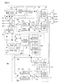
- a digital camera 10 includes a zoom lens 12, a focus lens 14, and an aperture unit 16 respectively driven by drivers 20a, 20b, and 20c.
- An optical image of an object scene is irradiated onto an imaging surface of a CMOS-type image sensor 18 through these members.
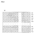
- the imaging surface is provided with an effective pixel area equivalent to horizontal 3072 pixels ⁇ vertical 1728 pixels, and is covered with a color filter 18f in a Bayer array of primary colors shown in Figure 2 . Electric charges produced in each pixel have any one of color information, i.e., R (Red), G (Green), and B (Blue).
- a CPU 36 applies a corresponding command to a driver 20d in order to execute a through-image process.
- the driver 20d exposes the imaging surface in response to a vertical synchronization signal Vsync generated for each 1/30 seconds from an SG (Signal Generator) 22, and reads out the electric charges produced thereby from the imaging surface.
- the image sensor 18 has four channels CH1 to CH4, and raw image data (original image data) based on the read-out electric charges are outputted dispersively (in a parallel manner) from the channels CH1 to CH4.
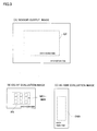
- the outputted raw image data has a resolution of horizontal 3072 pixels ⁇ vertical 1728 pixels, as shown in Figure 3(A) .
- the raw image data to be outputted has G pixels and B pixels alternately placed in horizontal lines at odd numbers, and has R pixels and G pixels alternately placed in horizontal lines at even numbers.
- a pre processing circuit 24 respectively performs a parallel pre-process of four systems on the 4-channel raw image data outputted from the image sensor 18.
- the pre process of each system is configured by a noise removal, a reduction zoom, and an edge adjustment, and the raw image data (zoom image data) that has undergone such a pre-process is written into a raw image area 42a of an SDRAM 42 through a memory control circuit 40.
- the reduction zoom in the pro-processing circuit 24 is executed by a zoom circuit 24z.
- the reduction zoom executed by the zoom circuit 24z is defined as "RAW zoom”.
- the raw image data (resolution: horizontal 3072 pixels ⁇ vertical 1728 pixels) from which the noise is removed by the pre-processing circuit 24 is also applied to evaluation-image creating circuits 26 and 28.
- the evaluation-image creating circuit 26 performs a process for adding vertical two pixels each other to the applied raw image data and a process for adding horizontal two pixels each other to the same so as to create EIS/AF evaluation image data.
- the evaluation-image creating circuit 28 performs a process for adding horizontal four pixels each other to the applied raw image data so as to create AE/AWB evaluation image data.
- the EIS/AF evaluation image data has a resolution of horizontal 1536 pixels ⁇ vertical 864 pixels, as shown in Figure 3(B) .
- the AE/AWB evaluation image data has a resolution of horizontal 768 pixels ⁇ vertical 1728 pixels, as shown in Figure 3(C) .
- the EIS/AF evaluation image data is applied to a motion detecting circuit 30 and an AF evaluating circuit 32, and the AE/AWB evaluation image data is applied to an AE/AWB evaluating circuit 34.
- one extraction area EX and nine motion detection areas MD1 to MD9 are allocated to the imaging surface.
- the extraction area EX has a size equivalent to horizontal 1920 pixels ⁇ vertical 1080 pixels.
- the motion detection areas MD 1 to MD3 are lined up in a horizontal direction at an upper level of the imaging surface
- the motion detection areas MD4 to MD6 are lined up in a horizontal direction at a middle level of the imaging surface
- the motion detection areas MD7 to MD9 are lined up in a horizontal direction at a lower level of the imaging surface.
- the motion detecting circuit 30 detects a partial motion vector representing motion of the object scene in each of the motion detection areas MD 1 to MD9 based on the EIS/AF evaluation image data, and combines together the detected partial motion vectors so as to create a total motion vector. Both the process for detecting the partial motion vectors and the process for creating the total motion vector are executed at each generation of the vertical synchronization signal Vsync.
- the CPU 36 determines which one of two factors, i.e., a camera shake and a pan/tilt operation, causes the motion of the imaging surface in a direction orthogonal to an optical axis.
- the CPU 36 moves the extraction area EX along the total motion vector.
- a position of the extraction area EX is changed so that the motion of the imaging surface caused due to the camera shake is compensated (offset). It is noted that a focus area FA and a photometric/white balance area EWA described later are moved along with the movement of the extraction area EX.
- a post-processing circuit 44 reads out the partial raw image data belonging to the extraction area EX, out of the raw image data accommodated in the raw image area 42a, through the memory control circuit 40, and performs post-processes, such as a color separation, a white balance adjustment, a YUV conversion, and an enlargement zoom, on the read-out partial raw image data.
- the partial raw image data is read out from the raw image area 42a in response to the vertical synchronization signal Vsync, and the post-process is executed also in response to the vertical synchronization signal Vsync.
- the thus-produced image data of a YUV format is outputted from a moving-image output terminal M_OUT, and written into a moving image area 42b of the SDRAM 42 through the memory control circuit 40.
- each of a plurality of pixels forming the image data on which the color separating process is performed in the post-processing circuit 44 has all color information of R, G, and B.
- the format of such image data is converted to a YUV format by the YUV conversion, and the enlargement zoom is further performed thereon.
- the enlargement zoom in the post-processing circuit 44 is executed by a zoom circuit 44z.
- the enlargement zoom executed by the post-processing circuit 44 is defined as "YUV zoom”.
- An LCD driver 46 repeatedly reads out the image data accommodated in the moving image area 42b, and drives an LCD monitor 48 based on the read-out image data. As a result, a real-time moving image (through image) representing the object scene is displayed on a monitor screen.
- the AE/AWB evaluating circuit 34 integrates one portion of the AE/AWB evaluation image data belonging to a photometric/white balance area EWA shown in Figure 3(C) , out of the AE/AWB evaluation image data outputted from the evaluation-image creating circuit 28, at each generation of the vertical synchronization signal Vsync, and outputs an integral value, i.e., an AE/AWB evaluation value.
- the CPU 36 executes an AE/AWB process in order to calculate an appropriate EV value and an appropriate white balance adjustment gain based on the AE/AWB evaluation value outputted from the AE/AWB evaluating circuit 34.
- An aperture amount and an exposure time period that define the calculated appropriate EV value are set to the drivers 20c and 20d, respectively, and the calculated appropriate white balance adjustment gain is set to the post-processing circuit 44. As a result, a brightness and a white balance of the moving image outputted from the LCD monitor 48 are moderately adjusted
- the AF evaluating circuit 32 extracts one portion of the EIS/AF evaluation image data belonging to the focus area FA shown in Figure 3(B) , out of the EIS/AF evaluation image data outputted from the evaluation-image creating circuit 26, and integrates a high-frequency component of the extracted EIS/AF evaluation image data in response to the vertical synchronization signal Vsync.
- the calculated integral value i.e., the AF evaluation value
- the CPU 36 refers to the applied AF evaluation value so as to continually search a focal point by a so-called hill-climbing process.
- the focus lens 14 is placed at the discovered focal point.
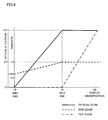
- the optical zoom magnification indicates “1.0" when the zoom lens 12 is positioned at a wide end, and indicates “10.0" when the zoom lens 12 is positioned at a tele end Furthermore, the optical zoom magnification increases linearly as the zoom lens 12 moves from the wide end to the tele end, and is maintained at "10.0" in a range that the display magnification exceeds "16".
- the YUV zoom magnification is maintained at "1.0” in a range that the display magnification is equal to or less than "16", and increases linearly up to "10.0" in a range that the display magnification exceeds "16".
- the CPU 36 sets the calculated optical zoom magnification, RAW zoom magnification, and YUV zoom magnification, to the driver 20a, the zoom circuit 24z, and the zoom circuit 44z, respectively, in order to execute the zoom process.
- the through image having the target display magnification is outputted from the LCD monitor 48.
- the CPU 36 changes settings of the motion detection areas MD 1 to MD9, the focus area FA, and the photometric/white balance area EWA so as to be adapted to the RAW zoom magnification set to the zoom circuit 24z. This improves the accuracy of the image-stabilizing process, the continuous AF process, and the AE/AWB process.
- the CPU 36 applies a recording start command to an I/F 50 in order to start a moving-image recording process.
- the I/F 50 creates a moving image file within a recording medium 52, cyclically reads out the image data accommodated in the moving image area 42b, and writes the read-out image data into the moving image file within the recording medium 52.
- a recording stop command is applied to the I/F 50.
- the I/F 50 ends reading-out of the image data from the moving image area 42b, and closes the moving image file of a write destination. Thereby, the moving image file is completed.
- the CPU 36 applies a still-image extracting command to the post-processing circuit 44 and also applies a still-image recording command to the I/F 50.
- the post-processing circuit 44 outputs one frame of image data representing an object scene image obtained at a time point when the shutter button 38s is manipulated, from a still-image output terminal S_OUT.
- the outputted image data is written into the still image area 42b of the SDRAM 42 through the memory control circuit 40.
- the I/F 50 reads out the image data accommodated in a still image area 42c, through the memory control circuit 40, and creates a still image file in which the read-out image data is contained, within the recording medium 52.
- the CPU 36 sets the RAW zoom magnification and the YUV zoom magnification (both indicating "1.0") to the zoom circuits 24z and 44z, and applies the still-image processing command and the still-image recording command to the pre-processing circuit 24, the post-processing circuit 44, and the I/F 50, respectively.
- one frame of raw image data having a resolution of horizontal 3072 pixels ⁇ vertical 1728 pixels is outputted from the pre-processing circuit 24, and written into the raw image area 42a of the SDRAM 42.
- the post-processing circuit 44 reads out the raw image data having the same resolution from the raw image area 42a, and outputs YUV-fomatted image data that is based on the read-out raw image data, from the still-image output terminal S_OUT.
- the outputted image data is written into the still image area 42c of the SDRAM 42 through the memory control circuit 40.
- the I/F 50 reads out the image data accommodated in the still image area 42c through the memory control circuit 40, and creates a still image file in which the read-out image data is contained, within the recording medium 52. Upon completion of recording, the above-mentioned through-image process is resumed
- the image sensor 18 is configured as shown in Figure 5 .
- the electric charges representing the object scene image are produced by a plurality of light-receiving elements 56, 56, ..., placed in a matrix.
- Each of the light-receiving elements 56 is equivalent to the above-described pixel.
- Each of light-receiving elements 56, 56, ..., lined up in a vertical direction is connected to a common CDS circuit 62 via an A/D converter 58 and a row selecting switch 60.
- the electric charge produced in each light-receiving element 56 is converted into 12-bit digital data by the A/D converter 58.
- a vertical scanning circuit 66 executes an operation for turning on/off each of the row selecting switches 60, 60, ..., for each pixel, in a raster scanning manner. Noise included in the pixel data that has undergone the row selecting switch 60 that is in a turned-on state is removed by the CDS circuit 62.
- a column selecting switch 641 is allocated to a CDS circuit 62 in a (4N+1)th (N: 0,1, 2, 3, ...) column, a column selecting switch 642 is allocated to a CDS circuit 62 in a (4N+2)th column, a column selecting switch 643 is allocated to a CDS circuit 62 in a (4N+3)th column, and a column selecting switch 644 is allocated to a CDS circuit 62 in a (4N+4)th column.
- a horizontal scanning circuit 68 turns on the column selecting switch 641 at a timing at which the row selecting switch 60 in a (4N+1)th column is turned on, turns on the column selecting switch 642 at a timing at which the row selecting switch 60 in a (4N+2)th column is turned on, turns on the column selecting switch 643 at a timing at which the row selecting switch 60 in a (4N+3)th column is turned on, and turns on the column selecting switch 644 at a timing at which the row selecting switch 60 in a (4N+4)th column is turned on.
- the partial raw image data based on the electric charge produced in the light-receiving element 56 in the (4N+1)th column is outputted from the channel CH1
- the partial raw image data based on the electric charge produced in the light-receiving element 56 in the (4N+2)th column is outputted from the channel CH2.
- the partial raw image data based on the electric charge produced in the light-receiving element 56 in the (4N+3)th column is outputted from the channel CH3
- the partial raw image data based on the electric charge produced in the light-receiving element 56 in the (4N+4)th column is outputted from the channel CH4.
- the pre-processing circuit 24 is configured as shown in Figure 6 .
- the partial raw image data of the channel CH1 is applied to the zoom circuit 24z via an LPF 24f1
- the partial raw image data of the channel CH2 is applied to the zoom circuit 24z via an LPF 24f2.
- the partial raw image data of the channel CH3 is applied to the zoom circuit 24z via an LPF 24f3
- the partial raw image data of the channel CH4 is applied to the zoom circuit 24z via an LPF 24f4.
- the partial raw image data of four channels outputted from the LPF24fl to 24f4 is also outputted toward the evaluation-image creating circuits 26 and 28. Furthermore, the zoom circuit 24z performs a reduction zoom on the applied raw image data, i.e., the original image data, and outputs the raw image data having a reduced size, i.e., the zoom image data.
- the partial raw image data corresponding to the channel CH1 is applied to an edge adjusting circuit 24e1
- the partial raw image data corresponding to the channel CH2 is applied to an edge adjusting circuit 24e2.
- the partial raw image data corresponding to the channel CH3 is applied to an edge adjusting circuit 24e3
- the partial raw image data corresponding to the channel CH4 is applied to an edge adjusting circuit 24e4.
- the raw image data on which the edge adjustment is performed by the edge adjusting circuits 24e1 to 24e4 are later written into an SRAM 24m.
- a controller 24c issues a write request toward the memory control circuit 40 each time an amount of data accommodated in the SRAM 24m reaches a threshold value, and outputs the raw image data of a predetermined amount toward the memory control circuit 40 when an approval signal is sent back from an issuance destination.
- the zoom circuit 24z is configured as shown in Figure 7 .
- the raw image data of the channel CH1 is applied to a divider 70a, and the raw image data of the channel CH2 is applied to a divider 70b.
- the raw image data of the channel CH3 is applied to a divider 70c, and the raw image data of the channel CH4 is applied to a divider 70d.
- each raw image data of the channels CH1 and CH3 has a B pixel corresponding to a horizontal line at an odd number and a G pixel corresponding to a horizontal line at an even number.
- each raw image data of the channels CH2 and CH4 has a G pixel corresponding to a horizontal line at an odd number and has an R pixel corresponding to a horizontal line at an even number.
- Each of the dividers 70a and 70c applies the G pixel to a color separating circuit 74 and an SRAM 72configuring a color separating system CS2, and applies the B pixel to a selector 92 configuring a color separating system CS 1.
- each of the dividers 70b and 70d applies the G pixel to the color separating circuit 74 and the SRAM 72, and applies the R pixel to the selector 92.
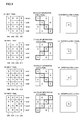
- the color separating circuit 74 performs a linear, color interpolating process on the two G pixels directly inputted from the dividers 70a to 70d and the two G pixels read out from the SRAM 72, or the four G pixels read out from the SRAM 72, and outputs an interpolated G pixel created thereby toward a horizontal zoom circuit 76 configuring a zoom system VS2.
- the horizontal zoom circuit 76 performs a horizontal zoom process (linear interpolating process in a horizontal direction) that is with reference to the RAW zoom magnification set by the CPU 36, on the interpolated G pixel continuously outputted from the color separating circuit 74, i.e., the interpolated image data having the G color information.
- the interpolated G pixel on which the horizontal zoom process is performed is defined as an "H zoom G pixel”
- the H zoom G pixel is created as shown in Figure 10(B) based on the interpolated G pixel shown in Figure 10(A) .
- the horizontal zoom circuit 76 executes the horizontal zoom process in four parallels corresponding to the channels CH1 to CH4 on an output side, and simultaneously outputs the four H zoom G pixels lined up in a horizontal direction.
- the simultaneously outputted four H zoom G pixels are applied to a divider 80.
- the divider 80 writes the H zoom G pixels corresponding to the channels CH1 and CH3, into an SRAM 82a, and writes the H zoom G pixels corresponding to the channels CH2 and CH4, into an SRAM 82b.
- a selector 84 reads out the three H zoom G pixels corresponding to the channel CH1 on the output side and the three H zoom G pixels corresponding to the channel CH3 on the output side from the SRAM 82a. Out of these, the three H zoom G pixels corresponding to the channel CH1 undergo dividers 86b to 86d to be inputted into the vertical zoom circuit 88a, and the three H zoom G pixels corresponding to the channel CH3 undergo the dividers 86b to 86d to be inputted into the vertical zoom circuit 88b.
- the selector 84 furthermore reads out the three H zoom G pixels corresponding to the channel CH2 and the three H zoom G pixels corresponding to the channel CH4, from the SRAM 82b.
- the three H zoom G pixels corresponding to the channel CH2 undergo the dividers 86b to 86d to be inputted into the vertical zoom circuit 88a, and the three H zoom G pixels corresponding to the channel CH4 undergo the dividers 86b to 86d to be inputted into the vertical zoom circuit 88b.
- the four H zoom G pixels simultaneously outputted from the horizontal zoom circuit 76 are also applied to a divider 86a
- the divider 86a inputs the one H zoom G pixel corresponding to the channel CH1, into the vertical zoom circuit 88a, and inputs the one H zoom G pixel corresponding to the channel CH3, into the vertical zoom circuit 88b.
- the divider 86a inputs the one H zoom G pixel corresponding to the channel CH2, into the vertical zoom circuit 88a, and inputs the one H zoom G pixel corresponding to the channel CH4, into the vertical zoom circuit 88b.
- the vertical zoom circuit 88a When the line to be noticed is the horizontal line at an even number, the vertical zoom circuit 88a performs a vertical zoom process (linear interpolating process in a vertical direction) that is with reference to the RAW zoom magnification set by the CPU 36, on the four H zoom G pixels corresponding to the channel CH1 on the output side. When the line to be noticed is the horizontal line at an odd number, the vertical zoom circuit 88a further performs a similar vertical zoom process, on the four H zoom G pixels corresponding to the channel CH2 on the output side. From the vertical zoom circuit 88a, the one HV zoom G pixel based on the four H zoom G pixels that are subject to the vertical zoom process is outputted.
- the vertical zoom circuit 88b performs the vertical zoom process that is with reference to the RAW zoom magnification set by the CPU 36, on the four H zoom G pixels corresponding to the channel CH3 on the output side.
- the vertical zoom circuit 88b further performs a similar vertical zoom process, on the four H zoom G pixels corresponding to the channel CH4 on the output side.
- the one HV zoom G pixel is outputted based on the four H zoom G pixels that are subject to the vertical zoom process.
- HV zoom G pixels shown in Figure 10(C) are created based on horizontal zoom G pixels shown in Figure 10(B) .
- HV zoom G pixels shown in Figure 10(D) are created.
- the zoom image data having the G color information is formed by the HV zoom pixels thus created.
- the R pixel is detected from the channels CH2 and CH4 in the horizontal line at an even number
- the B pixel is detected from the channels CH1 and CH3 in the horizontal line at an odd number.
- the selector 92 applies the two R pixels detected from the horizontal line at an even number, to one input terminal of a selector 94 and an SRAM 96, and applies the two B pixels detected from the horizontal line at an odd number, to the other input terminal of the selector 94 and an SRAM 98.
- the selector 94 selects the one input terminal when the two R pixels are outputted from the selector 92, and selects the other input terminal when the two B pixels are outputted from the selector 92.
- a selector 100 reads out the R pixel from the SRAM 96 corresponding to the color interpolating process of the R pixel, and reads out the B pixel from the SRAM 98 corresponding to the color interpolating process of the B pixel.
- a color separating circuit 102 performs a linear color interpolating process on the two R pixels inputted from the selector 94 and the one R pixel inputted from the selector 100 or the three R pixels inputted from the selector 100 so as to create an interpolated R pixel.
- the color separating circuit 102 also performs a linear color-interpolating process on the two B pixels inputted from the selector 94 and the one B pixel inputted from the selector 100 or the three B pixels inputted from the selector 100 so as to create an interpolated B pixel.
- the color interpolating process for creating the interpolated R pixel and the color interpolating process for creating the interpolated B pixel are alternately executed in a horizontal direction.
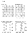
- the interpolated R pixel is created corresponding to pixel patterns shown in Figure 11(A), Figure 11(C) , Figure 12(A), and Figure 12(C) .
- the interpolated B pixel is created corresponding to pixel patterns shown in Figure 11(B), Figure 11(D) , Figure 12(B), and Figure 12(D) .
- the interpolated image data having the R color information is formed by the interpolated R pixel thus created.
- the interpolated image data having the B color information is formed by the interpolated B pixel thus created
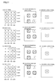
- the interpolated R pixel and the interpolated B pixel corresponding to the horizontal line at an odd number are applied to a horizontal zoom & horizontal thinning-out circuit 104a configuring a zoom system VS1 (see Figure 13(A) ).
- the interpolated R pixel and the interpolated B pixel corresponding to the horizontal line at an even number are applied to a horizontal zoom & horizontal thinning-out circuit 104b (see Figure 13(B) ).
- the horizontal zoom & thinning-out circuit 104a performs a horizontal zoom process that is with reference to the RAW zoom magnification set by the CPU 36 and a 1/2 thinning-out process, on an interpolated R pixel and an interpolated B pixel shown in Figure 13(A) . Also the horizontal zoom & thinning-out circuit 104b performs a similar horizontal zoom process and 1/2 thinning-out process, on an interpolated R pixel and an interpolated B pixel shown in Figure 13(B) .
- the R pixel and the B pixel on which the horizontal zoom process and the 1/2 thinning-out process are performed are defined as an "H zoom R pixel" and an "H zoom B pixel", respectively.
- an H zoom R pixel and an H zoom B pixel shown in Figure 13(C) are outputted from the horizontal zoom & thinning-cut circuit 104a, and an H zoom R pixel and an H zoom B pixel shown in Figure 13(D) are outputted from the horizontal zoom & thinning-out circuit 104b.
- each of the horizontal zoom & thinning-out circuits 104a and 104b executes the horizontal zoom process and the 1/2 thinning-out process in four parallels corresponding to the channels CH1 to CH4, and simultaneously outputs the four H zoom R pixels/H zoom B pixels lined up in a horizontal direction.
- the four H zoom R pixels/H zoom B pixels simultaneously outputted from the horizontal zoom & thinning-out circuit 104a are applied to one input terminal of the selector 106. Also, the four H zoom R pixels/H zoom B pixels simultaneously outputted from the horizontal zoom & thinning-out circuit 104b are applied to the other input terminal of the selector 106.
- the selector 106 writes the H zoom B pixels corresponding to the channels CH1 and CH3, into an SRAM 108a, and writes the H zoom R pixels corresponding to the channels CH2 and CH4, into an SRAM 108b.
- a selector 110 reads out the two H zoom R pixels corresponding to the channel CH2 on the output side and the two H zoom R pixels corresponding to the channel CH4 on the output side, from the SRAM 108a Out of these, the two H zoom R pixels corresponding to the channel CH2 undergo the dividers 112c to 112d to be inputted into the vertical zoom circuit 114a, and the two H zoom R pixels corresponding to the channel CH4 undergo the dividers 112c to 112d to be inputted into the vertical zoom circuit 114b.
- the selector 110 reads out the two H zoom B pixels corresponding to the channel CH1, and reads out the two H zoom B pixels corresponding to the channel CH3, from the SRAM 108a
- the two H zoom B pixels corresponding to the channel CH1 undergo the dividers 112c to 112d to be inputted into the vertical zoom circuit 114a
- the two H zoom B pixels corresponding to the channel CH3 undergo the dividers 112c to 112d to be inputted into the vertical zoom circuit 114b.
- the four H zoom R pixels/H zoom B pixels simultaneously outputted from the horizontal zoom & thinning-out circuit 104a are also applied to the divider 112a.
- the four H zoom R pixels/H zoom B pixels simultaneously outputted from the horizontal zoom & thinning-out circuit 104b are applied also to the divider 112b.
- each of the dividers 112a and 112b inputs the one H zoom R pixel corresponding to the channel CH2, into the vertical zoom circuit 114a, and inputs the one H zoom R pixel corresponding to the channel CH4, into the vertical zoom circuit 114b.
- each of the dividers 112a and 112b inputs the one H zoom B pixel corresponding to the channel CH1, into the vertical zoom circuit 114a, and inputs the one H zoom B pixel corresponding to the channel CH3, into the vertical zoom circuit 114b.
- the vertical zoom circuit 114a When the line to be noticed is the horizontal line at an even number, the vertical zoom circuit 114a performs a vertical zoom process (linear interpolating process in a vertical direction) that is with reference to the RAW zoom magnification set by the CPU 36, on the four H zoom R pixels corresponding to the channel CH2. When the line to be noticed is the horizontal line at an odd number, the vertical zoom circuit 114a further performs a similar vertical zoom process, on the four H zoom B pixels corresponding to the channel CH1. From the vertical zoom circuit 114a, the one HV zoom R pixel based on the four H zoom R pixels that are subject to the vertical zoom process, or the one HV zoom B pixel based on the four H zoom B pixels that are subj ect to the vertical zoom process is outputted.
- the vertical zoom circuit 114b When the line to be noticed is the horizontal line at an even number, also the vertical zoom circuit 114b performs the vertical zoom process that is with reference to the RAW zoom magnification set by the CPU 36, on the four H zoom R pixels corresponding to the channel CH4. When the line to be noticed is the horizontal line at an odd number, the vertical zoom circuit 114b further performs a similar vertical zoom process, on the four H zoom B pixels corresponding to the channel CH3. Also from the vertical zoom circuit 114b, the one HV zoom R pixel based on the four H zoom R pixels that are subject to the vertical zoom process, or the one HV zoom B pixel based on the four H zoom B pixels that are subject to the vertical zoom process is outputted.
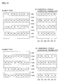
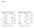
- an HV zoom R pixel and an HV zoom B pixel shown in Figure 14(A) are created.
- an HV zoom R pixel and an HV zoom B pixel shown in Figure 14(B) are created.
- the zoom image data having the R color information is formed by the HV zoom R pixel thus created.
- the zoom image data having the B color information is formed by the HV zoom B pixel thus created.
- the HV zoom G pixel shown in Figure 15(A) is applied.
- an HV zoom R pixel and an HV zoom B pixel shown in Figure 15(B) are applied.
- the selector 90 sorts out the applied HV zoom G pixel, HV zoom R pixel, and HV zoom B pixel, depending on each channel.
- the RAW data having a pixel pattern shown in Figure 15(C) i.e., the zoom image data, is obtained.
- the dividers 70a to 70d fetch the original image in which a plurality of original pixels, each of which has any one of R, G, and B, are arrayed in a Bayer manner (predetermined manner).
- the color separating systems CS1 and CS2 performs a color interpolating process on the fetched raw image so as to create the interpolated image formed by the plurality of interpolated pixels, each of which has the two colors.
- the zoom systems VS1 and VS2 performs a zoom process on the interpolated image created by the color separating systems CS 1 and CS2 so as to create a zoom image in which a plurality of zoom pixels are arrayed in a Bayer manner, each of which has any one of R, G, and B.
- the interpolated image is created by the color interpolating process for the original image, the interpolated image has more color information than the original image does.
- the zoom image is created by the zoom process for such an interpolated image. Thereby, the quality of the zoom image is improved
- the zoom image has the same color array as that of the original image, and each pixel forming the interpolated image has one portion of the colors.
- the interpolated image is created by the color interpolating process for the original image, and the zoom image is created by the zoom process for the interpolated image. Thereby, it becomes possible to inhibit a circuit scale.
- an image in which a plurality of pixels, each of which has R, G, or B, are arrayed in a Bayer manner is assumed as the original image.
- the two colors i.e., two colors of G and R or the two colors of G and B
- the number of colors allocated to each pixel by the color interpolating process may be appropriately changed in a range which is two or more and falls below the number of colors adopted by the original image.
- the types of colors allocated to each pixel by the color interpolating process may also be appropriately changed according to the types of colors adopted by the original image.
- the four output channels are arranged in the image sensor, and the four pixels lined up in a horizontal direction are simultaneously outputted
- the number of horizontal pixels to be simultaneously outputted may be optionally different from "4" as long as the number is equal to or more than "2".
- the interpolated R pixel and the interpolated B pixel corresponding to the horizontal line at an odd number are applied to the horizontal zoom & horizontal thinning-out circuit 104a, and at the same time, the interpolated R pixel and the interpolated B pixel corresponding to the horizontal line at an even number are applied to the horizontal zoom & horizontal thinning-out circuit 104b.
- the interpolated R pixel may be optionally applied to the horizontal zoom & horizontal thinning-out circuit 104a
- the interpolated B pixel may be optionally applied to the horizontal zoom & horizontal thinning-out circuit 104b.
- the configuration of the horizontal zoom & horizontal thinning-out circuits 104a and 104b at a later stage needs to be changed as well.
Landscapes
- Engineering & Computer Science (AREA)
- Physics & Mathematics (AREA)
- General Physics & Mathematics (AREA)
- Theoretical Computer Science (AREA)
- Multimedia (AREA)
- Signal Processing (AREA)
- Color Television Image Signal Generators (AREA)
- Studio Devices (AREA)
- Color Image Communication Systems (AREA)
- Facsimile Image Signal Circuits (AREA)
Applications Claiming Priority (1)
| Application Number | Priority Date | Filing Date | Title |
|---|---|---|---|
| JP2009010339A JP5191407B2 (ja) | 2009-01-20 | 2009-01-20 | 画像処理装置 |
Publications (2)
| Publication Number | Publication Date |
|---|---|
| EP2211304A2 true EP2211304A2 (de) | 2010-07-28 |
| EP2211304A3 EP2211304A3 (de) | 2013-08-07 |
Family
ID=42173630
Family Applications (1)
| Application Number | Title | Priority Date | Filing Date |
|---|---|---|---|
| EP10000479.5A Withdrawn EP2211304A3 (de) | 2009-01-20 | 2010-01-19 | Bildverarbeitungsvorrichtung |
Country Status (5)
| Country | Link |
|---|---|
| US (1) | US20100182460A1 (de) |
| EP (1) | EP2211304A3 (de) |
| JP (1) | JP5191407B2 (de) |
| KR (1) | KR20100085862A (de) |
| CN (1) | CN101783962A (de) |
Cited By (1)
| Publication number | Priority date | Publication date | Assignee | Title |
|---|---|---|---|---|
| WO2019036112A1 (en) * | 2017-08-16 | 2019-02-21 | Qualcomm Incorporated | IMAGE CAPTURE DEVICE WITH STABILIZED EXPOSURE OR WHITE BALANCING |
Families Citing this family (3)
| Publication number | Priority date | Publication date | Assignee | Title |
|---|---|---|---|---|
| JP5748513B2 (ja) * | 2011-03-07 | 2015-07-15 | 株式会社ザクティ | 撮像装置 |
| US8879858B1 (en) | 2013-10-01 | 2014-11-04 | Gopro, Inc. | Multi-channel bit packing engine |
| CN108259759A (zh) * | 2018-03-20 | 2018-07-06 | 北京小米移动软件有限公司 | 对焦方法、装置及存储介质 |
Citations (1)
| Publication number | Priority date | Publication date | Assignee | Title |
|---|---|---|---|---|
| JP2009010339A (ja) | 2007-05-30 | 2009-01-15 | Nec Electronics Corp | 半導体装置 |
Family Cites Families (17)
| Publication number | Priority date | Publication date | Assignee | Title |
|---|---|---|---|---|
| JPH03282497A (ja) * | 1990-03-30 | 1991-12-12 | Toshiba Corp | 信号変換方式および装置 |
| US5652621A (en) * | 1996-02-23 | 1997-07-29 | Eastman Kodak Company | Adaptive color plane interpolation in single sensor color electronic camera |
| JP3503372B2 (ja) * | 1996-11-26 | 2004-03-02 | ミノルタ株式会社 | 画素補間装置及びその画素補間方法 |
| JP4045645B2 (ja) * | 1998-05-19 | 2008-02-13 | 株式会社ニコン | 補間処理装置および補間処理プログラムを記録した記録媒体 |
| US6236433B1 (en) * | 1998-09-29 | 2001-05-22 | Intel Corporation | Scaling algorithm for efficient color representation/recovery in video |
| JP5108172B2 (ja) * | 2000-09-06 | 2012-12-26 | 株式会社ニコン | 画像データサイズ変換処理装置、電子スチルカメラ、および画像データサイズ変換処理用記録媒体 |
| CN1756371A (zh) * | 2001-01-25 | 2006-04-05 | 株式会社尼康 | 图像处理方法、图像处理程序、图像处理装置 |
| US6989862B2 (en) * | 2001-08-23 | 2006-01-24 | Agilent Technologies, Inc. | System and method for concurrently demosaicing and resizing raw data images |
| WO2003024094A1 (en) * | 2001-09-10 | 2003-03-20 | Nikon Corporation | Digital camera system, image storage apparatus, and digital camera |
| JP2004241813A (ja) * | 2003-02-03 | 2004-08-26 | Fuji Photo Film Co Ltd | 撮像装置およびデジタル画像処理方法 |
| JP4104495B2 (ja) * | 2003-06-18 | 2008-06-18 | シャープ株式会社 | データ処理装置、画像処理装置およびカメラ |
| US7688364B2 (en) * | 2004-12-10 | 2010-03-30 | Ambarella, Inc. | Decimating and cropping based zoom factor for a digital camera |
| JP4840967B2 (ja) * | 2005-12-01 | 2011-12-21 | キヤノン株式会社 | 撮像装置及び画像処理方法及びプログラム及び記憶媒体 |
| CN100527792C (zh) * | 2006-02-07 | 2009-08-12 | 日本胜利株式会社 | 摄像方法以及摄像装置 |
| JP4802944B2 (ja) * | 2006-08-31 | 2011-10-26 | 大日本印刷株式会社 | 補間演算装置 |
| JP5053654B2 (ja) * | 2007-02-09 | 2012-10-17 | オリンパスイメージング株式会社 | 画像処理装置およびその方法と電子カメラ |
| JP2009005166A (ja) * | 2007-06-22 | 2009-01-08 | Olympus Corp | 色補間装置及び画像処理システム |
-
2009
- 2009-01-20 JP JP2009010339A patent/JP5191407B2/ja not_active Expired - Fee Related
-
2010
- 2010-01-19 EP EP10000479.5A patent/EP2211304A3/de not_active Withdrawn
- 2010-01-19 KR KR1020100004828A patent/KR20100085862A/ko not_active Withdrawn
- 2010-01-20 US US12/690,416 patent/US20100182460A1/en not_active Abandoned
- 2010-01-20 CN CN201010004677A patent/CN101783962A/zh active Pending
Patent Citations (1)
| Publication number | Priority date | Publication date | Assignee | Title |
|---|---|---|---|---|
| JP2009010339A (ja) | 2007-05-30 | 2009-01-15 | Nec Electronics Corp | 半導体装置 |
Cited By (3)
| Publication number | Priority date | Publication date | Assignee | Title |
|---|---|---|---|---|
| WO2019036112A1 (en) * | 2017-08-16 | 2019-02-21 | Qualcomm Incorporated | IMAGE CAPTURE DEVICE WITH STABILIZED EXPOSURE OR WHITE BALANCING |
| US10491832B2 (en) | 2017-08-16 | 2019-11-26 | Qualcomm Incorporated | Image capture device with stabilized exposure or white balance |
| CN111034170A (zh) * | 2017-08-16 | 2020-04-17 | 高通股份有限公司 | 具有稳定曝光或白平衡的图像捕获装置 |
Also Published As
| Publication number | Publication date |
|---|---|
| US20100182460A1 (en) | 2010-07-22 |
| CN101783962A (zh) | 2010-07-21 |
| EP2211304A3 (de) | 2013-08-07 |
| JP2010171548A (ja) | 2010-08-05 |
| KR20100085862A (ko) | 2010-07-29 |
| JP5191407B2 (ja) | 2013-05-08 |
Similar Documents
| Publication | Publication Date | Title |
|---|---|---|
| EP3217647B1 (de) | Bildgebungsvorrichtung, bildgebungsverfahren und verarbeitungsprogramm | |
| JP4980982B2 (ja) | 撮像装置、撮像方法、合焦制御方法及びプログラム | |
| US8253812B2 (en) | Video camera which adopts a focal-plane electronic shutter system | |
| EP2882183B1 (de) | Elektronische Vorrichtung und Verfahren zur Steuerung davon | |
| EP2690875A1 (de) | Farbbildsensor, bildgebungsvorrichtung und steuerprogramm für die bildgebungsvorrichtung | |
| EP2355491A1 (de) | Abbildungsvorrichtung, Abbildungsverfahren und Abbildungsprogramm | |
| JP7142507B2 (ja) | 画像処理装置および画像処理方法、ならびに撮像装置 | |
| US10187594B2 (en) | Image pickup apparatus, image pickup method, and non-transitory computer-readable medium storing computer program | |
| JP4435228B2 (ja) | 撮像装置、およびその制御方法 | |
| EP2753068A2 (de) | Bildaufnahmevorrichtung | |
| JP2006324834A (ja) | 撮像装置及び撮像方法 | |
| US8836821B2 (en) | Electronic camera | |
| US20100182460A1 (en) | Image processing apparatus | |
| US9148634B2 (en) | Imaging device, method for controlling imaging device, and storage medium storing a control program where a basic color filter array pattern is repeated to reduce false color generation when image is thinned | |
| US8120668B2 (en) | Electronic camera for adjusting a parameter for regulating an image quality based on the image data outputted from an image sensor | |
| JP2006245999A (ja) | 撮像装置、およびプログラム | |
| JP2009077321A (ja) | 画像記録装置及び画像記録処理方法 | |
| JP5239250B2 (ja) | 電子カメラ | |
| JP2010239267A (ja) | 撮像装置、周辺減光補正制御方法およびプログラム | |
| JP5127731B2 (ja) | ビデオカメラ | |
| JP2006352717A (ja) | デジタルカメラ、及びその画像処理方法 | |
| JP4940291B2 (ja) | 撮像装置、およびその制御方法 | |
| JP2011176458A (ja) | デジタルカメラ | |
| JP2006115074A (ja) | 撮像装置及び撮像方法 | |
| CN119485044A (zh) | 图像处理设备、图像处理方法、摄像设备、存储介质及计算机程序产品 |
Legal Events
| Date | Code | Title | Description |
|---|---|---|---|
| PUAI | Public reference made under article 153(3) epc to a published international application that has entered the european phase |
Free format text: ORIGINAL CODE: 0009012 |
|
| AK | Designated contracting states |
Kind code of ref document: A2 Designated state(s): AT BE BG CH CY CZ DE DK EE ES FI FR GB GR HR HU IE IS IT LI LT LU LV MC MK MT NL NO PL PT RO SE SI SK SM TR |
|
| AX | Request for extension of the european patent |
Extension state: AL BA RS |
|
| PUAL | Search report despatched |
Free format text: ORIGINAL CODE: 0009013 |
|
| AK | Designated contracting states |
Kind code of ref document: A3 Designated state(s): AT BE BG CH CY CZ DE DK EE ES FI FR GB GR HR HU IE IS IT LI LT LU LV MC MK MT NL NO PL PT RO SE SI SK SM TR |
|
| AX | Request for extension of the european patent |
Extension state: AL BA RS |
|
| RIC1 | Information provided on ipc code assigned before grant |
Ipc: G06T 3/40 20060101AFI20130701BHEP |
|
| STAA | Information on the status of an ep patent application or granted ep patent |
Free format text: STATUS: THE APPLICATION HAS BEEN WITHDRAWN |
|
| 18W | Application withdrawn |
Effective date: 20130909 |