EP2209211A2 - Statischer Hochspannungsschalter - Google Patents
Statischer Hochspannungsschalter Download PDFInfo
- Publication number
- EP2209211A2 EP2209211A2 EP09354052A EP09354052A EP2209211A2 EP 2209211 A2 EP2209211 A2 EP 2209211A2 EP 09354052 A EP09354052 A EP 09354052A EP 09354052 A EP09354052 A EP 09354052A EP 2209211 A2 EP2209211 A2 EP 2209211A2
- Authority
- EP
- European Patent Office
- Prior art keywords
- transistor
- control
- current
- switching means
- voltage
- Prior art date
- Legal status (The legal status is an assumption and is not a legal conclusion. Google has not performed a legal analysis and makes no representation as to the accuracy of the status listed.)
- Granted
Links
Images

Classifications
-
- H—ELECTRICITY
- H03—ELECTRONIC CIRCUITRY
- H03K—PULSE TECHNIQUE
- H03K17/00—Electronic switching or gating, i.e. not by contact-making and –breaking
- H03K17/08—Modifications for protecting switching circuit against overcurrent or overvoltage
- H03K17/082—Modifications for protecting switching circuit against overcurrent or overvoltage by feedback from the output to the control circuit
- H03K17/0828—Modifications for protecting switching circuit against overcurrent or overvoltage by feedback from the output to the control circuit in composite switches
-
- H—ELECTRICITY
- H03—ELECTRONIC CIRCUITRY
- H03K—PULSE TECHNIQUE
- H03K17/00—Electronic switching or gating, i.e. not by contact-making and –breaking
- H03K17/51—Electronic switching or gating, i.e. not by contact-making and –breaking characterised by the components used
- H03K17/56—Electronic switching or gating, i.e. not by contact-making and –breaking characterised by the components used by the use, as active elements, of semiconductor devices
- H03K17/567—Circuits characterised by the use of more than one type of semiconductor device, e.g. BIMOS, composite devices such as IGBT
Definitions
- the invention relates to a high-voltage static switch intended to be connected in series with a load to be protected.
- the switch comprises at least two electrical switching means connected in parallel, measuring means for measuring an electrical voltage across the electrical switching means and a main current flowing in the load.
- the switch also comprises control means delivering a control signal to act on the opening and closing of the electrical switching means as a function of the value of the main electric current flowing through the load.
- the power components used to perform the electrical switching function are widely used in particular in the aeronautical field.
- these components may be MOSFET, IGBT, BIPOLAR, JFET, silicon or silicon carbide transistors.
- the switching devices used as a static switch are subsequently called SSPC (Solid State Power Controler) or CDS (Solid State Switch).
- a SSPC type static switch is adapted to operate generally according to two modes of operation.
- a first mode of operation corresponds to the case where the electric current has a value less than or equal to the rated current In of operation (I ⁇ In).
- the SSPC type switch must then have a small drop in voltage. This voltage drop across the circuit breaker SSPC is called thereafter waste voltage. Reducing the waste voltage reduces Joule losses in the circuit breaker. In addition, reducing the waste voltage makes it possible to increase the amount of energy transferred to the load. A maximum of energy can be transferred to the load when the voltage of waste is minimal. By way of example, the maximum acceptable waste voltage may be 0.4V
- a second mode of operation corresponds to the case where the electric current has a value greater than the nominal operating current (I> In).
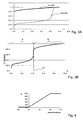
- the SSPC type switch is generally able to withstand a high current (I> In) for a shorter time as the value of the current is high. This overcurrent, and the time during which it is applied, is given by the disjunction curve as represented in FIG. figure 2 .
- the maximum acceptable waste voltage may be 2V.
- IGBT type transistors in SSPC circuit breakers are known. Its use is more particularly dedicated to high voltage applications. In particular conditions of use, especially when the temperature is approximately equal to 150 ° C. and the current is less than one tenth of the maximum current, then the waste voltage of the IGBT type transistors can not be less than 0.85. volt. This waste voltage is closer to 1.15V under normal operating conditions. This makes it necessary to increase the efficiency of the cooling devices which are then heavy and bulky. This is a handicap for the use of SSPC switches in aeronautics.
- the document FR2680925 describes the use of a first bipolar type transistor connected in parallel with an IGBT type transistor.
- this type of assembly has a low waste voltage.
- this type of assembly has the particular disadvantage of having a low gain.
- the assembly consisting of an IGBT type transistor and a bipolar transistor connected in parallel can therefore not open quickly in case of overcurrent.
- the invention therefore aims to overcome the disadvantages of the state of the art, so as to provide a high voltage static switch with low energy losses.
- the high voltage static switch according to the invention is characterized in that the conduction state of the first electrical switching means depends both on the main current flowing in the load, a control current, a control voltage delivered. by the control means, and the gain of the first electrical switching means.
- the first switching means comprises a first bipolar transistor connected in series with a second field effect transistor, the emitter of the first bipolar type transistor being connected to the drain of the second field effect transistor.
- control means are connected to the base of the first bipolar type transistor in order to deliver a controlled control current, said regulated control current being dependent on both a reference voltage, the main electric current and a waste voltage measured between the collector of the bipolar transistor and the source of the second field effect transistor.
- the control means are connected to the gate of the second field effect transistor to output a control signal.
- the first switching means comprises an ESBT® type transistor.
- control means are connected to the base of the ESBT®-type transistor in order to deliver a controlled control current, said regulated control current being dependent on both a reference voltage, the main electric current and a waste voltage measured between the collector and the source of said transistor.
- the control means are connected between the base and the source of said transistor to output a control signal.
- the second electrical switching means comprises a third transistor.
- the third transistor is a bipolar IGBT type gate transistor
- the control means are connected to the gate of said IGBT type bipolar transistor type to provide a control signal.
- the third transistor is a MOSFET field effect transistor
- the control means are connected to the gate of said field effect transistor to deliver a control signal.
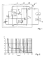
- the high-voltage static switching device 1 comprises at least two electrical switching means 2A, 2B connected in parallel. Said at least two electrical switching means are of different technology. In other words, the electrical switching means respectively connected in parallel are different from each other.
- the static switching device is intended to be connected to a load 3.
- Measuring means 4 are intended for measuring an electrical voltage Vcs across the electrical switching means 2A, 2B and a main current Ic flowing in the load 3.
- the measuring means 4 are connected to control means 5.
- control means 5 are intended to deliver a control signal Vcom, Ib to act on the opening and closing of the electrical switching means 2A, 2B as a function of the value of the main electric current Ic passing through the load 3.
- Vcom control signal
- Ib control signal
- the conduction state of the first electrical switching means 2A depends on the main current Ic flowing in the load 3 and the gain Hfe of the first electrical switching means 2A.
- control means 5 are connected to the first electrical switching means 2A so that the conduction state of said first electrical switching means 2A depends both on a current of command Ib and a control voltage Vcom delivered by the control means 5.
- the first electrical switching means 2A comprises a CASCODE-type circuit comprising two transistors T1, T2.
- a first bipolar transistor T1 is connected in series with a second field effect transistor T2 (MOSFET type).
- the emitter E of the first transistor of the type bipolar T1 is connected to the drain D of the second field effect transistor T2.
- the control means 5 are intended to deliver a control signal Vcom to the gate of the second field effect transistor T2.
- the third transistor T3 is preferably a bipolar IGBT type gate transistor.
- the control means 5 are electrically connected to the transistors T1, T2, T3. Indeed, the control means 5 are connected to the base of the first bipolar transistor T1 to provide a regulated control current Ib. Said control current Ib is dependent on both a reference voltage Vref, the main electric current Ic and a waste voltage Vcs measured between the collector C of the first bipolar type transistor T1 and the source S of the second field effect transistor of the MOSFET type T2.
- the control means 5 are also connected to the gate of the second field effect transistor of MOSFET type T2 to output a control signal Vcom.
- the control means 5 are connected to the gate of said IGBT type bipolar IGBT transistor to provide a control signal Vcom.
- the operating principle of the second electrical switching means 2B comprising the third transistor T3 is as follows.
- the second electrical switching means 2B is conductive when the control means 5 deliver a control voltage Vcom.
- Vcom control voltage
- Vcom waste voltage
- Ic main current
- the operating principle of the first electrical switching means 2A comprising the CASCODE circuit is different from that of the second electrical switching means 2B.
- the conduction state of the first electrical switching means 2A (blocked, limited or saturated) depends on both the main current Ic flowing in the load 3, the control current Ib, the control voltage Vcom, and the gain Hfe of the bipolar type transistor T1.
- the first electrical switching means 2A is conductive when a Control voltage Vcom is present and a control current Ib supplies the base of the first bipolar type transistor T1.
- the transistor T2 of the MOSFET type is conductive if the control voltage Vcom is applied. He then behaves like a resistance with a given Ron value.
- the internal resistance value Ron is an example of 0.08 ohm in this first embodiment.
- the waste voltage Vce of the first electrical switching means 2A is then between 0.1V and 0.5V and can be considered as low.
- the waste voltage tends to increase very rapidly.
- the bipolar type transistor T1 has a mode of operation as described below.
- the bipolar type transistor T1 is saturated if the control current Ib is greater than the ratio Ic / Hfe between the main current Ic and the gain Hfe.
- the waste voltage Vce may then be less than 0.3 volts.
- the bipolar transistor T1 is conductive if the control current Ib is both greater than 0 and less than the ratio Ic / Hfe between the main current and the gain Hfe.
- the waste voltage Vce then tends to increase.
- Transistor T1 of bipolar type is blocked if control current Ib is equal to 0.
- This solution would not be economical because it would be necessary to size the electrical circuit so that it is able to provide a maximum control current Ib sufficient for the regulation can withstand the main currents Ic greater than the nominal current In.
- control current Ib is increased as the waste voltage Vce is greater than a reference voltage Vref, and decreases Ib when the waste voltage Vce is lower than the reference voltage Vref.
- the value of the control current Ib is bounded between a minimum and a maximum.
- a first minimum value is very small to maintain the first transistor T1 bipolar conduction even if the load 3 consumes no main current Ic.
- a second maximum value is sufficient for the regulation to operate up to a nominal current In, but not beyond.
- control current Ib follows a variation proportional to the value of the main current Ic.
- the control current Ib is kept slightly lower than the ratio Ic / Hfe between the main current and the gain Hfe.
- the first bipolar type transistor T1 is then not completely saturated.
- the waste voltage used for the regulation could be chosen between 0.25V and 1V. These values are defined as follows: The minimum of 0.25V is the lowest value that can guarantee the transistors T1, T2 of the assembly CASCODE, and the highest value (1V) is that which could guarantee the third transistor T3 type IGBT.
- the choice of the value of the waste voltage Vce for regulation is determined as a function of the total electrical losses when the main current Ic is equal to the nominal current In. It is sought to optimize the operation of the device by minimizing these total electrical losses.
- the total electrical losses in the first switching means 2A consist, on the one hand, of direct electrical losses in the transistors T1, T2 of the CASCODE assembly and, on the other hand, of electrical losses due to the control of the first bipolar transistor T1.
- the loss Direct electric in the circuit CASCODE are equal to the product of the waste voltage Vce of the first switching means 2A by the main current Ic (Vce x Ic).
- the electrical losses due to the control of the first bipolar transistor T1 are equal to the product of the supply voltage Valim of the circuit generating the control current Ib at the base of the first bipolar transistor T1 by the control current Ib (FIG. Valim x Ib).
- the regulation of the waste voltage Vce of the first switching means 2A is between 0.3 and 0.4 V.
- control means 5 The operation of the control means 5 is as follows.
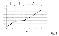
- a main current Ic passing through the load 3 is between the value of the nominal current In and a short-circuit current Icc (zone B)
- said main current Ic flows in both the first and the second means of switching 2A, 2B.
- the distribution of the main current Ic in the electrical switching means 2A, 2B is as follows: an electric current of approximately equal value to that of the nominal current In flows in the first switching means 2A and a current of approximately equal value the difference between the main current Ic and the nominal current In (Ic - In) in the second switching means 2B.
- the first bipolar transistor T1 connected in series with the second MOSFET transistor T2 according to a CASCODE circuit is advantageously replaced by an ESBT® type transistor (Emitter-Switched Bipolar Transistors).
- the first electrical switching means 2A then comprises a single ESBT® type transistor which then integrates the functionalities of the first and second transistors T1, T2.
- the control means 5 are connected to the base of the ESBT® type transistor to supply a controlled control current Ib. Said control current Ib is then dependent on both a reference voltage Vref, the main electric current Ic and a waste voltage Vcs measured between the collector C and the source of said transistor.
- the control means 5 are connected between the base and the source of said transistor to output a control signal Vcom.
- the operating principle of the ESBT® type transistor is as follows, it leads when the control voltage Vcom is present, is that a control current Ib is supplied thereto. Its conduction state (blocked, limited or saturated) depends on the value of the main current Ic, the command current Ib, and the gain Hfe of said transistor.
- the first electrical switching means 2A comprises either a CASCODE circuit having a first and second transistor T1, T2 or an ESBT® type transistor.
- the second electrical switching means 2B comprises a third MOSFET field effect transistor T3 instead of an IGBT type transistor.
- the control means 5 are connected to the gate of said field effect transistor to provide a control signal Vcom.
- the control of the first electrical switching means is identical to that of the two preferred modes described above.
- the third MOSFET transistor T3 of the second switching means 2B is conductive if the control voltage Vcom is applied. It then behaves like an internal resistance having a given value Ron.
- the resistance value Ron is an example of 0.12 ohm in this embodiment. Said transistor has a linear behavior.
- control means The operation of the control means is as follows.
Landscapes
- Electronic Switches (AREA)
Applications Claiming Priority (1)
| Application Number | Priority Date | Filing Date | Title |
|---|---|---|---|
| FR0900242A FR2941338B1 (fr) | 2009-01-20 | 2009-01-20 | Commutateur statique haute tension |
Publications (3)
| Publication Number | Publication Date |
|---|---|
| EP2209211A2 true EP2209211A2 (de) | 2010-07-21 |
| EP2209211A3 EP2209211A3 (de) | 2010-12-22 |
| EP2209211B1 EP2209211B1 (de) | 2018-10-24 |
Family
ID=40972882
Family Applications (1)
| Application Number | Title | Priority Date | Filing Date |
|---|---|---|---|
| EP09354052.4A Active EP2209211B1 (de) | 2009-01-20 | 2009-12-04 | Statischer Hochspannungsschalter |
Country Status (3)
| Country | Link |
|---|---|
| US (1) | US8089303B2 (de) |
| EP (1) | EP2209211B1 (de) |
| FR (1) | FR2941338B1 (de) |
Families Citing this family (4)
| Publication number | Priority date | Publication date | Assignee | Title |
|---|---|---|---|---|
| US9093866B2 (en) | 2011-12-02 | 2015-07-28 | Hamilton Sundstrand Corporation | Configurable power switching controller |
| US9178355B2 (en) | 2011-12-02 | 2015-11-03 | Hamilton Sundstrand Corporation | Cross communication arrangement for multiple solid state power controller channels |
| US9160174B2 (en) | 2011-12-02 | 2015-10-13 | Hamilton Sundstrand Corporation | Control architecture for power switching controller |
| DE102017204052A1 (de) | 2017-03-13 | 2018-09-13 | Zf Friedrichshafen Ag | Verfahren und Steuergerät zum Bestimmen eines Spannungsabfalls eines elektronischen Bauelements |
Citations (1)
| Publication number | Priority date | Publication date | Assignee | Title |
|---|---|---|---|---|
| FR2680925A1 (fr) | 1991-08-27 | 1993-03-05 | Sextant Avionique | Interrupteur statique a faibles pertes. |
Family Cites Families (10)
| Publication number | Priority date | Publication date | Assignee | Title |
|---|---|---|---|---|
| US5153457A (en) * | 1990-12-12 | 1992-10-06 | Texas Instruments Incorporated | Output buffer with di/dt and dv/dt and tri-state control |
| JP2837054B2 (ja) * | 1992-09-04 | 1998-12-14 | 三菱電機株式会社 | 絶縁ゲート型半導体装置 |
| JP3084982B2 (ja) * | 1992-11-25 | 2000-09-04 | 富士電機株式会社 | 半導体装置 |
| DE69731501T2 (de) * | 1996-05-17 | 2005-10-20 | Denso Corp., Kariya | Lastbetätigungsschaltung |
| FR2794890B1 (fr) * | 1999-06-08 | 2001-08-10 | Crouzet Automatismes | Relais electromecanique assiste a la commutation par semi-conducteur |
| US6404173B1 (en) * | 2000-07-28 | 2002-06-11 | Iwatt | Linear AC to DC regulator with synchronous rectification |
| US7362079B1 (en) * | 2004-03-03 | 2008-04-22 | Cypress Semiconductor Corporation | Voltage regulator circuit |
| JP2006053898A (ja) * | 2004-07-15 | 2006-02-23 | Rohm Co Ltd | 過電流保護回路およびそれを利用した電圧生成回路ならびに電子機器 |
| JP2007221473A (ja) * | 2006-02-16 | 2007-08-30 | Nissan Motor Co Ltd | スイッチング回路の駆動回路及びスイッチング回路 |
| US8488289B2 (en) * | 2006-09-27 | 2013-07-16 | International Rectifier Corporation | Current protection circuit for intelligent power switch |
-
2009
- 2009-01-20 FR FR0900242A patent/FR2941338B1/fr not_active Expired - Fee Related
- 2009-12-04 EP EP09354052.4A patent/EP2209211B1/de active Active
-
2010
- 2010-01-07 US US12/654,870 patent/US8089303B2/en active Active
Patent Citations (1)
| Publication number | Priority date | Publication date | Assignee | Title |
|---|---|---|---|---|
| FR2680925A1 (fr) | 1991-08-27 | 1993-03-05 | Sextant Avionique | Interrupteur statique a faibles pertes. |
Also Published As
| Publication number | Publication date |
|---|---|
| EP2209211B1 (de) | 2018-10-24 |
| FR2941338B1 (fr) | 2016-11-04 |
| US20100182071A1 (en) | 2010-07-22 |
| FR2941338A1 (fr) | 2010-07-23 |
| US8089303B2 (en) | 2012-01-03 |
| EP2209211A3 (de) | 2010-12-22 |
Similar Documents
| Publication | Publication Date | Title |
|---|---|---|
| EP2926443B1 (de) | Dc/dc wandler für hohe spannungen mit jfet schaltelement | |
| FR2928056A1 (fr) | Dispositif de protection d'un variateur de vitesse contre les surintensites. | |
| FR2693853A1 (fr) | Circuit de protection d'un composant de puissance contre des surtensions directes. | |
| FR2710191A1 (fr) | MOSFET de puissance avec protection de sur-intensité et de surchauffe. | |
| EP1950885A1 (de) | Steuervorrichtung eines elektronischen Leistungstrenners und eine solche Vorrichtung umfassender Stromrichter | |
| EP2209211B1 (de) | Statischer Hochspannungsschalter | |
| FR2931594A1 (fr) | Dispositif de protection d'un circuit electrique contre les surtensions | |
| FR3006515A1 (fr) | Protection electrique a l'aide d'un interrupteur a semi-conducteur. | |
| EP3267583B1 (de) | Auswahlschaltkreis einer betriebsspannung mit kontolliertem übergang | |
| EP3435505A1 (de) | Kontrollverfahren von einschaltströmen, die bevorzugt durch einen lastschalter fliessen, und entsprechender elektronischer schaltkreis | |
| EP2073367B1 (de) | Wechselspannungsgenerator ausgestattet mit einem Strombegrenzer | |
| FR2547133A1 (fr) | Circuit destine a prevenir une dissipation excessive d'energie dans les dispositifs commutateurs de puissance | |
| EP1977514B1 (de) | Steuerung eines mos-transistors | |
| FR2691306A1 (fr) | Amplificateur avec limitation de courant de sortie. | |
| EP1992069B1 (de) | Einrichtung zur steuerung eines mos-transistors | |
| WO2010086237A1 (fr) | Dispositif de commande d'un transistor jfet | |
| EP4199345A1 (de) | Vorrichtung und verfahren zur überwachung eines elektrischen energiewandlers, zugehöriges elektrisches energieumwandlungssystem | |
| EP4070455B1 (de) | Aktive entladevorrichtung und -verfahren | |
| FR2889775A1 (fr) | Procede et montage de limitation de la dissipation d'un commutateur de puissance a semi-conducteur. | |
| EP2293443B1 (de) | Elektronisches Steuermodul für einen JFET Transistor | |
| EP0164770B1 (de) | Statisches Relais für niedrige Gleichstromspannung | |
| EP3664294B1 (de) | Schutzvorrichtung eines versorgungssystems und messvorrichtung eines stroms in einem elektrischen schaltkreis, der eine solche schutzvorrichtung verwendet | |
| EP2198507B1 (de) | Variable steuerung | |
| WO2016102840A1 (fr) | Dispositif de controle pour ligne d'alimentation electrique | |
| FR3068847A1 (fr) | Dispositif de commutation pour transistor sic ou gan mosfet avec circuit de protection contre les surtensions et procede associe |
Legal Events
| Date | Code | Title | Description |
|---|---|---|---|
| PUAI | Public reference made under article 153(3) epc to a published international application that has entered the european phase |
Free format text: ORIGINAL CODE: 0009012 |
|
| AK | Designated contracting states |
Kind code of ref document: A2 Designated state(s): AT BE BG CH CY CZ DE DK EE ES FI FR GB GR HR HU IE IS IT LI LT LU LV MC MK MT NL NO PL PT RO SE SI SK SM TR |
|
| AX | Request for extension of the european patent |
Extension state: AL BA RS |
|
| PUAL | Search report despatched |
Free format text: ORIGINAL CODE: 0009013 |
|
| AK | Designated contracting states |
Kind code of ref document: A3 Designated state(s): AT BE BG CH CY CZ DE DK EE ES FI FR GB GR HR HU IE IS IT LI LT LU LV MC MK MT NL NO PL PT RO SE SI SK SM TR |
|
| AX | Request for extension of the european patent |
Extension state: AL BA RS |
|
| 17P | Request for examination filed |
Effective date: 20110621 |
|
| 17Q | First examination report despatched |
Effective date: 20170912 |
|
| REG | Reference to a national code |
Ref country code: DE Ref legal event code: R079 Ref document number: 602009055229 Country of ref document: DE Free format text: PREVIOUS MAIN CLASS: H03K0017000000 Ipc: H03K0017082000 |
|
| GRAP | Despatch of communication of intention to grant a patent |
Free format text: ORIGINAL CODE: EPIDOSNIGR1 |
|
| RIC1 | Information provided on ipc code assigned before grant |
Ipc: H03K 17/082 20060101AFI20180425BHEP Ipc: H03K 17/567 20060101ALI20180425BHEP |
|
| INTG | Intention to grant announced |
Effective date: 20180517 |
|
| GRAS | Grant fee paid |
Free format text: ORIGINAL CODE: EPIDOSNIGR3 |
|
| GRAA | (expected) grant |
Free format text: ORIGINAL CODE: 0009210 |
|
| AK | Designated contracting states |
Kind code of ref document: B1 Designated state(s): AT BE BG CH CY CZ DE DK EE ES FI FR GB GR HR HU IE IS IT LI LT LU LV MC MK MT NL NO PL PT RO SE SI SK SM TR |
|
| REG | Reference to a national code |
Ref country code: GB Ref legal event code: FG4D Free format text: NOT ENGLISH |
|
| REG | Reference to a national code |
Ref country code: CH Ref legal event code: EP |
|
| REG | Reference to a national code |
Ref country code: IE Ref legal event code: FG4D Free format text: LANGUAGE OF EP DOCUMENT: FRENCH |
|
| REG | Reference to a national code |
Ref country code: DE Ref legal event code: R096 Ref document number: 602009055229 Country of ref document: DE Ref country code: AT Ref legal event code: REF Ref document number: 1057877 Country of ref document: AT Kind code of ref document: T Effective date: 20181115 |
|
| REG | Reference to a national code |
Ref country code: NL Ref legal event code: MP Effective date: 20181024 |
|
| REG | Reference to a national code |
Ref country code: LT Ref legal event code: MG4D |
|
| REG | Reference to a national code |
Ref country code: AT Ref legal event code: MK05 Ref document number: 1057877 Country of ref document: AT Kind code of ref document: T Effective date: 20181024 |
|
| PG25 | Lapsed in a contracting state [announced via postgrant information from national office to epo] |
Ref country code: NL Free format text: LAPSE BECAUSE OF FAILURE TO SUBMIT A TRANSLATION OF THE DESCRIPTION OR TO PAY THE FEE WITHIN THE PRESCRIBED TIME-LIMIT Effective date: 20181024 |
|
| PG25 | Lapsed in a contracting state [announced via postgrant information from national office to epo] |
Ref country code: FI Free format text: LAPSE BECAUSE OF FAILURE TO SUBMIT A TRANSLATION OF THE DESCRIPTION OR TO PAY THE FEE WITHIN THE PRESCRIBED TIME-LIMIT Effective date: 20181024 Ref country code: BG Free format text: LAPSE BECAUSE OF FAILURE TO SUBMIT A TRANSLATION OF THE DESCRIPTION OR TO PAY THE FEE WITHIN THE PRESCRIBED TIME-LIMIT Effective date: 20190124 Ref country code: PL Free format text: LAPSE BECAUSE OF FAILURE TO SUBMIT A TRANSLATION OF THE DESCRIPTION OR TO PAY THE FEE WITHIN THE PRESCRIBED TIME-LIMIT Effective date: 20181024 Ref country code: HR Free format text: LAPSE BECAUSE OF FAILURE TO SUBMIT A TRANSLATION OF THE DESCRIPTION OR TO PAY THE FEE WITHIN THE PRESCRIBED TIME-LIMIT Effective date: 20181024 Ref country code: LV Free format text: LAPSE BECAUSE OF FAILURE TO SUBMIT A TRANSLATION OF THE DESCRIPTION OR TO PAY THE FEE WITHIN THE PRESCRIBED TIME-LIMIT Effective date: 20181024 Ref country code: AT Free format text: LAPSE BECAUSE OF FAILURE TO SUBMIT A TRANSLATION OF THE DESCRIPTION OR TO PAY THE FEE WITHIN THE PRESCRIBED TIME-LIMIT Effective date: 20181024 Ref country code: ES Free format text: LAPSE BECAUSE OF FAILURE TO SUBMIT A TRANSLATION OF THE DESCRIPTION OR TO PAY THE FEE WITHIN THE PRESCRIBED TIME-LIMIT Effective date: 20181024 Ref country code: LT Free format text: LAPSE BECAUSE OF FAILURE TO SUBMIT A TRANSLATION OF THE DESCRIPTION OR TO PAY THE FEE WITHIN THE PRESCRIBED TIME-LIMIT Effective date: 20181024 Ref country code: IS Free format text: LAPSE BECAUSE OF FAILURE TO SUBMIT A TRANSLATION OF THE DESCRIPTION OR TO PAY THE FEE WITHIN THE PRESCRIBED TIME-LIMIT Effective date: 20190224 Ref country code: NO Free format text: LAPSE BECAUSE OF FAILURE TO SUBMIT A TRANSLATION OF THE DESCRIPTION OR TO PAY THE FEE WITHIN THE PRESCRIBED TIME-LIMIT Effective date: 20190124 |
|
| PG25 | Lapsed in a contracting state [announced via postgrant information from national office to epo] |
Ref country code: PT Free format text: LAPSE BECAUSE OF FAILURE TO SUBMIT A TRANSLATION OF THE DESCRIPTION OR TO PAY THE FEE WITHIN THE PRESCRIBED TIME-LIMIT Effective date: 20190224 Ref country code: GR Free format text: LAPSE BECAUSE OF FAILURE TO SUBMIT A TRANSLATION OF THE DESCRIPTION OR TO PAY THE FEE WITHIN THE PRESCRIBED TIME-LIMIT Effective date: 20190125 Ref country code: SE Free format text: LAPSE BECAUSE OF FAILURE TO SUBMIT A TRANSLATION OF THE DESCRIPTION OR TO PAY THE FEE WITHIN THE PRESCRIBED TIME-LIMIT Effective date: 20181024 |
|
| REG | Reference to a national code |
Ref country code: DE Ref legal event code: R119 Ref document number: 602009055229 Country of ref document: DE |
|
| PG25 | Lapsed in a contracting state [announced via postgrant information from national office to epo] |
Ref country code: IT Free format text: LAPSE BECAUSE OF FAILURE TO SUBMIT A TRANSLATION OF THE DESCRIPTION OR TO PAY THE FEE WITHIN THE PRESCRIBED TIME-LIMIT Effective date: 20181024 Ref country code: CZ Free format text: LAPSE BECAUSE OF FAILURE TO SUBMIT A TRANSLATION OF THE DESCRIPTION OR TO PAY THE FEE WITHIN THE PRESCRIBED TIME-LIMIT Effective date: 20181024 Ref country code: DK Free format text: LAPSE BECAUSE OF FAILURE TO SUBMIT A TRANSLATION OF THE DESCRIPTION OR TO PAY THE FEE WITHIN THE PRESCRIBED TIME-LIMIT Effective date: 20181024 |
|
| REG | Reference to a national code |
Ref country code: CH Ref legal event code: PL |
|
| PG25 | Lapsed in a contracting state [announced via postgrant information from national office to epo] |
Ref country code: EE Free format text: LAPSE BECAUSE OF FAILURE TO SUBMIT A TRANSLATION OF THE DESCRIPTION OR TO PAY THE FEE WITHIN THE PRESCRIBED TIME-LIMIT Effective date: 20181024 Ref country code: SM Free format text: LAPSE BECAUSE OF FAILURE TO SUBMIT A TRANSLATION OF THE DESCRIPTION OR TO PAY THE FEE WITHIN THE PRESCRIBED TIME-LIMIT Effective date: 20181024 Ref country code: MC Free format text: LAPSE BECAUSE OF FAILURE TO SUBMIT A TRANSLATION OF THE DESCRIPTION OR TO PAY THE FEE WITHIN THE PRESCRIBED TIME-LIMIT Effective date: 20181024 Ref country code: SK Free format text: LAPSE BECAUSE OF FAILURE TO SUBMIT A TRANSLATION OF THE DESCRIPTION OR TO PAY THE FEE WITHIN THE PRESCRIBED TIME-LIMIT Effective date: 20181024 Ref country code: LU Free format text: LAPSE BECAUSE OF NON-PAYMENT OF DUE FEES Effective date: 20181204 Ref country code: RO Free format text: LAPSE BECAUSE OF FAILURE TO SUBMIT A TRANSLATION OF THE DESCRIPTION OR TO PAY THE FEE WITHIN THE PRESCRIBED TIME-LIMIT Effective date: 20181024 |
|
| PLBE | No opposition filed within time limit |
Free format text: ORIGINAL CODE: 0009261 |
|
| STAA | Information on the status of an ep patent application or granted ep patent |
Free format text: STATUS: NO OPPOSITION FILED WITHIN TIME LIMIT |
|
| REG | Reference to a national code |
Ref country code: IE Ref legal event code: MM4A |
|
| GBPC | Gb: european patent ceased through non-payment of renewal fee |
Effective date: 20190124 |
|
| 26N | No opposition filed |
Effective date: 20190725 |
|
| REG | Reference to a national code |
Ref country code: BE Ref legal event code: MM Effective date: 20181231 |
|
| PG25 | Lapsed in a contracting state [announced via postgrant information from national office to epo] |
Ref country code: DE Free format text: LAPSE BECAUSE OF NON-PAYMENT OF DUE FEES Effective date: 20190702 Ref country code: SI Free format text: LAPSE BECAUSE OF FAILURE TO SUBMIT A TRANSLATION OF THE DESCRIPTION OR TO PAY THE FEE WITHIN THE PRESCRIBED TIME-LIMIT Effective date: 20181024 Ref country code: IE Free format text: LAPSE BECAUSE OF NON-PAYMENT OF DUE FEES Effective date: 20181204 |
|
| PG25 | Lapsed in a contracting state [announced via postgrant information from national office to epo] |
Ref country code: BE Free format text: LAPSE BECAUSE OF NON-PAYMENT OF DUE FEES Effective date: 20181231 |
|
| PG25 | Lapsed in a contracting state [announced via postgrant information from national office to epo] |
Ref country code: GB Free format text: LAPSE BECAUSE OF NON-PAYMENT OF DUE FEES Effective date: 20190124 Ref country code: CH Free format text: LAPSE BECAUSE OF NON-PAYMENT OF DUE FEES Effective date: 20181231 Ref country code: LI Free format text: LAPSE BECAUSE OF NON-PAYMENT OF DUE FEES Effective date: 20181231 |
|
| PG25 | Lapsed in a contracting state [announced via postgrant information from national office to epo] |
Ref country code: MT Free format text: LAPSE BECAUSE OF FAILURE TO SUBMIT A TRANSLATION OF THE DESCRIPTION OR TO PAY THE FEE WITHIN THE PRESCRIBED TIME-LIMIT Effective date: 20181024 |
|
| PG25 | Lapsed in a contracting state [announced via postgrant information from national office to epo] |
Ref country code: TR Free format text: LAPSE BECAUSE OF FAILURE TO SUBMIT A TRANSLATION OF THE DESCRIPTION OR TO PAY THE FEE WITHIN THE PRESCRIBED TIME-LIMIT Effective date: 20181024 |
|
| PG25 | Lapsed in a contracting state [announced via postgrant information from national office to epo] |
Ref country code: HU Free format text: LAPSE BECAUSE OF FAILURE TO SUBMIT A TRANSLATION OF THE DESCRIPTION OR TO PAY THE FEE WITHIN THE PRESCRIBED TIME-LIMIT; INVALID AB INITIO Effective date: 20091204 Ref country code: CY Free format text: LAPSE BECAUSE OF FAILURE TO SUBMIT A TRANSLATION OF THE DESCRIPTION OR TO PAY THE FEE WITHIN THE PRESCRIBED TIME-LIMIT Effective date: 20181024 Ref country code: MK Free format text: LAPSE BECAUSE OF NON-PAYMENT OF DUE FEES Effective date: 20181024 |
|
| PGFP | Annual fee paid to national office [announced via postgrant information from national office to epo] |
Ref country code: FR Payment date: 20251111 Year of fee payment: 17 |