EP2205965B1 - Capteur chimique organique comprenant un polymère microporeux et procédé d'utilisation - Google Patents
Capteur chimique organique comprenant un polymère microporeux et procédé d'utilisation Download PDFInfo
- Publication number
- EP2205965B1 EP2205965B1 EP08834853.7A EP08834853A EP2205965B1 EP 2205965 B1 EP2205965 B1 EP 2205965B1 EP 08834853 A EP08834853 A EP 08834853A EP 2205965 B1 EP2205965 B1 EP 2205965B1
- Authority
- EP
- European Patent Office
- Prior art keywords
- sample
- sensing element
- analyte
- electrode
- electrodes
- Prior art date
- Legal status (The legal status is an assumption and is not a legal conclusion. Google has not performed a legal analysis and makes no representation as to the accuracy of the status listed.)
- Not-in-force
Links
Images


Classifications
-
- G—PHYSICS
- G01—MEASURING; TESTING
- G01N—INVESTIGATING OR ANALYSING MATERIALS BY DETERMINING THEIR CHEMICAL OR PHYSICAL PROPERTIES
- G01N27/00—Investigating or analysing materials by the use of electric, electrochemical, or magnetic means
- G01N27/26—Investigating or analysing materials by the use of electric, electrochemical, or magnetic means by investigating electrochemical variables; by using electrolysis or electrophoresis
- G01N27/28—Electrolytic cell components
- G01N27/30—Electrodes, e.g. test electrodes; Half-cells
-
- G—PHYSICS
- G01—MEASURING; TESTING
- G01N—INVESTIGATING OR ANALYSING MATERIALS BY DETERMINING THEIR CHEMICAL OR PHYSICAL PROPERTIES
- G01N27/00—Investigating or analysing materials by the use of electric, electrochemical, or magnetic means
- G01N27/02—Investigating or analysing materials by the use of electric, electrochemical, or magnetic means by investigating impedance
- G01N27/22—Investigating or analysing materials by the use of electric, electrochemical, or magnetic means by investigating impedance by investigating capacitance
- G01N27/221—Investigating or analysing materials by the use of electric, electrochemical, or magnetic means by investigating impedance by investigating capacitance by investigating the dielectric properties
Definitions
- the ability to detect chemical analytes, especially organic chemical analytes, is important in many applications, including environmental monitoring, and the like. Such detection and/or monitoring of organic molecules may find particular use in, for example, so called End of Service Life Indicators which are desired for personal protective equipment such as respirators.
- U.S. Patent Application Publication 2006/0249402 to Snow et al. discloses a sensing device having a bottom electrode, a dielectric on the bottom electrode, a grid of nanoelectrodes on the dielectric, and a top electrode in electrical contact with the grid.
- the nanoelectrodes may be a network of carbon nanotubes.
- U.S. Patent Application Publication 2006/0237310 to Patel et al. discloses a device that is described as being able to detect various target analytes by adsorption or absorption of the analyte in a chemical sensing material such that an electrical property (e.g. capacitance, resistance, etc.) is altered in a manner detectable by circuitry associated with the sensing electrode pair coated with the chemical sensing materials.
- an electrical property e.g. capacitance, resistance, etc.
- U.S. Patent 5,512,882 to Stetter and Maclay discloses a sensor whose impedance changes upon exposure to a vapor of a selected chemical substance.
- the sensor comprises a polymer whose physical structure is altered by the vapor (e.g., through expansion or disintegration).
- the sensor further comprises electrically conductive elements that are interspersed with the polymer. Changes can be measured by an impedance-measuring circuit.
- U.S. Patent 5,482,678 to Sittler discloses a sensor comprising a material which expands in the presence of an organic liquid, gas or vapor. The material is applied to a support surface such that upon expansion, the support deflects and changes the distance between two capacitor plates, thereby changing an electrical capacity between the plates.
- U.S. Patent 5,965,451 to Plog and Maunz discloses a gas sensor for selective detection of hydrocarbons, having a capacitive element and a gas-permeable sensitive layer as a dielectric.
- the sensitive layer is precious-metal-doped zeolite which has a regular crystalline structure made of primary pores whose diameter is on the order of the gas-kinetic diameter of the gas molecules to be detected.
- Japanese Patent Application Publication 06-281610 discloses a sensor having two electrodes with a poly(1-(trimethylsilyl)-1-propyne) film as dielectric in between whose impedance changes when exposed to water vapour, or to air containing 10% methanol or 10% acetone.
- a sensing element which is suitable for detecting or monitoring organic chemical analytes in an environment, for example in ambient atmosphere.
- a sensing element comprises an analyte-responsive dielectric material which is in proximity to first and second electrodes.
- an analyte-responsive dielectric material means a material that is capable of absorbing an organic chemical analyte, and that can exhibit a measurable change in an electrical property upon absorbing the organic analyte into the material.
- the analyte-responsive dielectric material exhibits a change in dielectric constant upon absorption of the analyte, such that a change in capacitance of the sensing element can be observed.
- the analyte-responsive dielectric material is a polymer of intrinsic microporosity.
- a material provides advantages in terms of high sensitivity to low levels of organic analytes, rapid response to organic analytes, and low sensitivity to water.
- applicant postulates that the performance that applicant has found in use of polymers of intrinsic microporosity as analyte-responsive dielectric materials may be due to any or all of several properties: hydrophobicity, an optimum amount of porosity, a microporous pore volume that encompasses an optimum pore size range, and the ability of the polymers of intrinsic microporosity to be cast from solution so as to form an analyte-responsive dielectric layer.
- Polymers of intrinsic microporosity can be formulated via the use of any combination of monomers that leads to a very rigid polymer and gives a polymer within which there are sufficient structural features to induce a contorted structure.
- such materials comprise organic macromolecules comprised of first generally planar species connected by rigid linkers, said rigid linkers having a point of contortion such that two adjacent first planar species connected by the linker are held in non-coplanar orientation.
- such materials can comprise organic macromolecules comprised of first generally planar species connected by rigid linkers predominantly to a maximum of two other said first species, said rigid linkers having a point of contortion such that two adjacent first planar species connected by the linker are held in non-coplanar orientation.
- such a point of contortion may comprise a spiro group, a bridged ring moiety or a sterically congested single covalent bond around which there is restricted rotation.
- a sensing element for sensing an organic chemical analyte according to claim 1.
- at least one of the electrodes is permeable to an organic chemical analyte.
- the permeable electrode is discontinuous.
- the permeable electrode is patterned.
- the sensing element can comprise a backing layer and/or a cover layer in proximity to at least one of the electrodes.
- the sensing element can comprise a parallel plate capacitor configuration, or an interdigitated capacitor configuration.
- a sensor for sensing an organic chemical analyte comprising: a sensing element according to claim 1 and, an operating circuit in electrical communication with the first and second electrodes, wherein the operating circuit is capable of applying a voltage to the first and second electrodes and is capable of detecting a change in an electrical property of the sensing element.
- a method of sensing organic chemical analytes comprising: providing a sensor according to claim 9; exposing the sensing element to an environment potentially containing one or more organic chemical analytes; applying a voltage to the first and second electrodes; and, monitoring an electrical property of the sensing element.
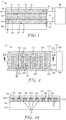
- a sensing element 1/101 that comprises at least an analyte-responsive dielectric layer 10/110 in proximity to a first electrode 20/120 and a second electrode 30/130.
- Fig. 1 depicts an exemplary sensing element based on the general configuration of a parallel plate capacitor
- Figs. 2, 2a , and 3 depict exemplary sensing elements based on the general configuration of an interdigitated capacitor.
- the various components have been given different reference numbers (generally, incremented by 100) in the Figs. depicting the different general configurations.
- the structure, composition and properties of the various components may be applicable to sensing elements of any capacitive design, unless otherwise stated.
- the sensing element 1/101 is configured such that the analyte-responsive dielectric layer 10/110 is in sufficiently close proximity to the first electrode 20/120 and the second electrode 30/130 that the analyte-responsive dielectric material contained in the layer will be capable of interacting with an electric field that is established by the electrodes.
- analyte-responsive dielectric layer 10/110 exhibits a change in an electrical property upon absorption of one or more analytes.
- the electrical property is capacitance or a capacitance-related property as described below.
- Such a change in a capacitance-related property can be measured by imparting a charge differential between the first electrode 20/120 and the second electrode 30/130 (e.g., by imparting a voltage differential to the electrodes) and monitoring the property of the sensing element in response to the presence of the analyte.
- Such monitoring can be done by the use of an operating circuit 28/128, as described later herein.
- capacitor and “capacitance-related property” encompass any electrical property and the measurement thereof that is in general associated with the imparting of an electrical charge (whether static or time variant) and the monitoring of an electrical property during and/or after the imparting of the charge.
- Such properties include not only capacitance, but also impedance, admittance, resistance, conductance, etc., and may be measured according to various methods known in the art.
- the analyte-responsive dielectric layer 10/110 (the term “layer” being used generically and encompassing any physical configuration) comprises at least in part an analyte-responsive dielectric material.
- analyte-responsive dielectric material means a material that is capable of absorbing an organic chemical analyte, and that can exhibit a measurable change in some electrical property of the material upon absorbing the organic analyte into the material.
- the analyte-responsive dielectric material is chosen from the family of materials comprising so-called "polymers of intrinsic microporosity” (hereafter called PIMs) as further defined in claim 1.
- PIMs polymers of intrinsic microporosity
- Such polymers include, but are not limited to, those disclosed in " Polymers of Intrinsic Microporosity (PIMs): Robust, Solution-Processable, Organic Microporous Materials," Budd et al., Chem. Commun., 2004, pp. 230-231 ; in “ Polymers of Intrinsic Microporosity (PIMs),” McKeown et al., Chem. Eur. J., 2005, 11, No. 9, 2610-2620 ; in US Patent Application Publication 2006/0246273 to McKeown et al. ; and in Published PCT application No. WO 2005/012397 A2 to McKeown et al.
- PIMs can be formulated via the use of any combination of monomers that lead to a very rigid polymer within which there are sufficient structural features to induce a contorted structure.
- PIMs according to the invention comprise organic macromolecules comprised of generally planar species connected by rigid linkers, said rigid linkers having a point of contortion such that two adjacent planar species connected by the linker are held in non-coplanar orientation.
- such materials can comprise organic macromolecules comprised of first generally planar species connected by rigid linkers predominantly to a maximum of two other said first species, said rigid linkers having a point of contortion such that two adjacent first planar species connected by the linker are held in non-coplanar orientation.
- such a point of contortion may comprise a spiro group, a bridged ring moiety or a sterically congested single covalent bond around which there is restricted rotation.
- PIMs have the advantage of possessing microporosity that is not significantly dependent on the thermal history of the material. PIMs thus may offer advantages in terms of being reproducibly manufacturable in large quantities, and in terms of not exhibiting properties that change upon aging, shelf life, etc.
- microporous and “microporosity” mean that the material has a significant amount of internal, interconnected pore volume, with the mean pore size (as characterized, for example, by sorption isotherm procedures) being less than about 100 nm.
- mean pore size as characterized, for example, by sorption isotherm procedures
- microporosity provides that molecules of organic analyte (if present) will be able to penetrate the internal pore volume of the material and take up residence in the internal pores.
- the presence of such analyte in the internal pores can alter the dielectric properties of the material such that a change in the dielectric constant (or any other suitable electrical property) can be observed.
- the disclosed sensing element 1/101 may have advantageous properties with regard to the sensing of an organic analyte, in that a measurable change in an electrical property of the dielectric material may be caused by the presence of the analyte molecules in the pores.
- a measurable change in an electrical property of the dielectric material may be caused by the presence of the analyte molecules in the pores.
- Such a microporous nature of the analyte-responsive dielectric material may contribute to increased sensitivity of the dielectric material to small amounts of organic analyte.
- the PIM comprises a porosity of at least about 10 %, at least about 20 %, or at least about 30 % (as characterized, for example, by sorption isotherm techniques, such as those using instruments available under the trade mark Autosorb from Quantachrome Instruments of Boynton Beach, Florida).
- porosity can provide good response to low levels of organic chemical analytes.
- the material should not have such a high pore volume that it is difficult to avoid electrical shorting or arcing between the first electrode 20/120 and the second electrode 30/130.
- the material comprises a porosity of at most about 90 %, at most about 60 % or at most about 40 %.
- the size and distribution of the internal pores may be such that at least some of the organic analyte molecules in at least some of the pores may form a more highly condensed state (e.g. a quasi-liquid state) than they would otherwise be in (e.g., than they would be in in the environment in which the analyte is monitored).
- a more highly condensed state e.g. a quasi-liquid state
- the analyte molecules collecting in the internal pores in larger numbers and/or at a higher concentration than they are present in the environment being monitored; in addition, or instead, the analyte molecules in this state may exhibit a higher dielectric constant (relative permittivity) than in an uncondensed vaporous or gaseous state.
- a sensing element based on a microporous analyte-responsive dielectric material with appropriately chosen size and distribution of pores may exhibit superior sensitivity to small quantities of organic analyte.
- the PIM comprises an average pore size of less about 50 nm, less than about 20 nm, or less than about 10 nm.
- the PIM comprises an average pore size of greater than about 0.3 nm, greater than about 0.5 nm, or greater than about 1.0 nm.
- the PIM is a hydrophobic organic polymeric material that will not absorb liquid water to an extent that the material swells significantly or otherwise exhibits a significant change in a physical property. Such hydrophobic properties are useful in providing an organic analyte sensing element that is relatively insensitive to the presence of water.
- the material may however comprise relatively polar moieties for specific purposes.
- the PIM comprises a continuous matrix.
- a continuous matrix is defined as an assembly (e.g. a coating, layer, etc.) in which the solid portion of the material is continuously interconnected (irrespective of the presence of porosity as described above, or of the presence of optional additives as discussed below). That is, a continuous matrix is distinguishable from an assembly that comprises an aggregation of particles (e.g. zeolites, activated carbons, carbon nanotubes, etc.).
- a layer or coating deposited from a solution will typically comprise a continuous matrix (even if the coating itself is applied in a patterned manner and/or comprises particulate additives).
- a collection of particles deposited via powder spraying, coating and drying of a dispersion e.g.
- a latex or by coating and drying of a sol-gel mixture, may not comprise a continuous network as defined by applicant.
- a latex, sol-gel, etc., layer can be consolidated such that individual particles are no longer discernible, nor is it possible to discern areas of the assembly that were obtained from different particles, such a layer may then meet applicant's definition of a continuous matrix.
- PIMs are soluble in common organic solvents and thus are amenable to conventional deposition processes such as coating.
- the material may be crosslinked using a suitable crosslinking agent, for example bis(benzonitrile)palladium(II) dichloride.
- a suitable crosslinking agent for example bis(benzonitrile)palladium(II) dichloride. This process may render the analyte-responsive dielectric layer insoluble in organic solvents, and/or may enhance certain physical properties such as durability, abrasion resistance, etc., which may be desirable in certain applications.
- the PIMs may be blended with other materials.
- the PIM may be blended with a material that itself is not an analyte-responsive dielectric material. Even though not contributing to an analyte response, such a material may be useful for other reasons. For example, such a material may allow the formation of a PIM-containing layer which has superior mechanical properties and the like.
- PIMs may be dissolved in a common solvent with the other material to form a homogeneous solution, which may be cast to form a analyte-responsive dielectric blend layer comprising both the PIM and the other polymer(s).
- PIMs may also be blended with a material that is an analyte-responsive dielectric material (for example, zeolites, activated carbon, silica gel, hypercrosslinked polymer networks and the like).
- a material that is an analyte-responsive dielectric material for example, zeolites, activated carbon, silica gel, hypercrosslinked polymer networks and the like.
- Such materials may comprise insoluble materials that are suspended in a solution comprising of a PIMs material. Coating and drying of such a solution/suspension may provide a composite analyte-responsive dielectric layer comprising both the PIM material and the additional analyte-responsive dielectric material.
- an additional layer or layers of material that is not an analyte-responsive dielectric material may be provided in proximity to the analyte-responsive dielectric layer.
- a layer or layers may be provided for any of a variety of reasons, e.g. as a protective layer, as a tie layer to improve adhesive, and so on.
- multiple individual layers of analyte-responsive dielectric material can be used.
- multiple layers of PIM materials can be used.
- one or more layers of some other analyte-responsive dielectric material can be used in addition to a layer of PIM material.
- the various layers of analyte-responsive dielectric material can be in direct contact with each other; or, they can be separated by a layer or layers present for some other purpose (e.g., passivation layers, tie layers, as described herein).
- the first electrode 20/120 and second electrode 30/130 can comprise any suitable conductive material. Combinations of different materials (conductive and/or nonconductive) can be used, as different layers or as a mixture, as long as sufficient overall conductivity is provided (e.g., the electrode material comprises a constant resistivity of less than about 10 -2 ohms-meter). Examples of materials that can be used to make the first electrode and/or second electrode include, but are not limited to, organic materials, inorganic materials, metals, alloys, and various mixtures and composites comprising any or all of these materials. In certain embodiments, coated (for example, vapor coated, sputter coated, etc.) metals or metal oxides, or combinations thereof, may be used.
- Suitable conductive materials include for example aluminum, tin, indium-tin oxide, gold, silver, platinum, palladium, copper, and the like.
- both electrodes comprise the same material; in an alternative embodiment, the first and second electrodes comprise different materials,
- either or both of the electrodes can be permeable to an organic analyte.
- Such electrode permeability may be particularly useful in the case of a sensing element which is configured in the general manner of a parallel-plate capacitor as shown in Fig. 1 .
- second electrode 30 is permeable, an organic analyte can enter analyte-responsive dielectric layer 10 through major surface 13, rather than having to enter the analyte-responsive dielectric layer 10 by way of edge 15, which might be a slower process.
- first electrode 20 is permeable, an organic analyte may be able to enter analyte-responsive dielectric layer 10 through major surface 11 (however, if backing 40 is not permeable to the analyte, it may not be useful to provide first electrode 20 in a permeable configuration).
- an electrode can be analyte-permeable by virtue of being discontinuous.
- discontinuous does not imply that the electrode comprises units (spots, islands, etc.) that are not in electrical contact with each other. Rather, discontinuous means that within the overall boundaries of the electrode, some areas do not contain conductive material.
- Such a discontinuous electrode may be microscopically discontinuous.
- an electrode can be formed by the deposition (e.g., by coating, ink-jet printing, etc.) of a sol comprising particles (e.g. nanoparticles) of a conductive material.
- the electrode comprises conductive particles that are in sufficient contact to ensure that the electrode is conductive, but with sufficient spaces in between the particles to render the electrode permeable to an organic analyte.
- an electrode can comprise a macroscopically discontinuous structure.
- a conductive material comprises vapor coated metal (which is typically impermeable)
- the conductive metal can be deposited in a pattern (for example, in a grid pattern, or in a "comb" pattern as disclosed in Example 1) rather than as a continuous layer.
- an electrically accessible area 25/125 of first electrode 20/120, and an electrically accessible area 35/135 of second electrode 30/130, are provided such that it is possible to connect an operating circuit 28/128 to the sensing element via these areas.
- Such electrically accessible areas can be provided in any convenient location. For example, such electrically accessible areas are shown on an edge of the electrodes in the exemplary illustrations of Figs. 1 and 2 , and are shown on a major surface (123 and 133) of the electrodes in the exemplary illustration of Fig. 3 .
- a connecting device e.g. a contact pad or tab
- 22/122 is positioned in contact with (e.g.
- a similar connecting device 32/132 can be likewise positioned in contact with the accessible area of the second electrode 30.
- a sensing element 1 can be produced which is configured in the general manner of a parallel-plate capacitor as shown in an exemplary manner in the cross sectional view of Fig. 1 .
- the sensing element comprises two generally planar, parallel, opposing electrodes, with the analyte-responsive dielectric layer being present in between the electrodes and preventing direct electrical contact between the two electrodes.
- a backing 40 is provided (which may be a continuous slab, layer or film of material) that is in proximity to at least one of the electrodes and that may serve to provide physical strength and integrity to the finished sensing element. Any suitable material may be used, including glass, ceramic, plastic, etc. In large scale production, a polymeric film (such as polyester) may be used. In some embodiments, the backing is an analyte-permeable material (for example, silicone rubber, a microporous membrane, etc.).
- a conductive layer that serves as first electrode 20 is provided on backing 40.
- the conductive layer may comprise any of the materials mentioned above, including blends or mixtures of conductive and nonconductive materials, and may be deposited by any suitable method, including but not limited to spin coating, dip coating, screen printing, transfer coating, sputter-coating, physical vapor deposition, chemical vapor deposition, or a combination of two or more of such methods.
- the conductive layer may be provided by placing a premade film (e.g. a metal foil, conductive tape, etc.) atop backing 40.
- This first electrode 20 may be provided as a continuous layer or as a discontinuous layer, as previously described.
- the conductive layer is provided such that a first surface 21 of electrode 20 is in proximity to, and/or in contact with, at least a portion of the first surface 41 of backing 40.
- an optional layer is present between at least a part of first surface 21 of electrode 20, and first surface 41 of backing 40. Such an optional layer may be used for any purpose (such as improving the bond between first electrode 20 and backing 40), as long as the layer does not interfere with the functioning of the sensing element 1.
- an analyte-responsive dielectric layer 10 is also provided.
- the analyte-responsive dielectric layer 10 is provided such that first major surface 11 of layer 10 is in direct contact with at least a portion of the second surface 23 of first electrode 20 (leaving at least a portion of first electrode 20 accessible for connection to an operating circuit).
- the analyte-responsive dielectric material is placed in proximity to the first electrode by a coating process, for example, including but not limited to solvent coating, spin coating, dip coating, transfer coating, screen printing, and the like.
- the dielectric material is deposited in such a manner as to minimize the presence of defects, pinholes, etc., that might serve to compromise the performance of the sensing element.
- the analyte-responsive dielectric layer comprises a polymer of intrinsic microporosity that is deposited by coating a solution of PIM material upon a suitable substrate and allowing the solution to dry so as to form a solid layer comprising the PIM material.
- An analyte-responsive dielectric layer 10 can also be provided by other methods.
- a preformed film of analyte-responsive dielectric material can be placed upon the second surface of the first electrode.
- the analyte-responsive dielectric material can be provided in particulate form (e.g. as a powder, as a suspension, or as a sol) and deposited in such a form onto a first electrode so as to form a particulate coating. If desired, such a material can be consolidated so as to form a continuous matrix of analyte-responsive dielectric material.
- a second electrode 30 can be formed by placing a second conductive layer in proximity to the analyte-responsive dielectric layer 10.
- the second electrode 30 may comprise conductive materials as described above, and may be deposited according to methods described above.
- the second electrode may comprise a discontinuous structure (again as previously described) so as to be permeable to an organic analyte.
- an optional protective cover or barrier layer 50 can be provided in proximity to at least one of the electrodes.
- cover layer 50 can be placed atop second electrode 30 (leaving an area of second electrode 30 accessible for electrical contact). Any such cover layer 50 should not significantly interfere with the functioning of sensing element 1.
- the sensing element is configured such that an analyte of interest must pass through cover layer 50 in order to reach the analyte-responsive dielectric layer 10, the cover layer should be sufficiently permeable to the analyte.
- Cover layer 50 may be deposited by any method known in the art, including coating (e.g. spin coating, dip coating, solvent coating, vapor coating, transfer coating, screen printing, flexographic printing, and the like).
- cover layer 50 can comprise a premade layer (e.g. a film or tape) that is placed upon second electrode 30.
- cover layer 50 is provided such that first surface 51 of cover layer 50 is in direct contact with at least a portion of second surface 33 of second electrode 30.
- the second surface of the cover layer may be the outermost surface of the sensing element, or may itself receive additional coatings or layers if desired.
- the second surface 23 of first electrode 20 and first major surface 11 of the analyte-responsive dielectric layer 10 are in direct contact, with no interposing layer(s) therebetween.
- the first surface 31 of second electrode 30 and second major surface 13 of the analyte-responsive dielectric layer 10 are in direct contact, with no interposing layer(s) therebetween.
- Such embodiments are pictured in Fig. 1 .
- other, optional layers may be present between the first electrode 20 and the analyte-responsive dielectric layer 10, and/or between the second electrode 30 and the analyte-responsive dielectric layer 10.
- either or both of the electrodes may not be in direct contact with some or all of a surface of the analyte-responsive dielectric material.
- a tie layer or layers may be used to improve the bonding between an electrode and the analyte-responsive dielectric layer.
- a passivation layer or layers (for example, a layer of silicon dioxide) may be placed in between a surface of the analyte-responsive dielectric layer and an electrode surface, in order to minimize the possibility of arcing between the electrodes.
- multiple such optional layers may be used; alternatively a single layer may serve multiple functions.
- any such optional layer or layers such as the aforementioned tie layers, passivation layers, protective layers, cover layers, etc., may be used, for whatever purpose, as long as they do not significantly interfere with the desired functioning of the sensing element.
- an optional layer should be sufficiently permeable to an analyte of interest if the sensing element is configured such that the analyte must pass through the optional layer in order to reach the analyte-responsive dielectric layer 10.
- edges of the various layers can be aligned flush with each other (as depicted in the exemplary embodiment of Fig. 1 ).
- various layers may overlap other layers, and/or the edges of certain layers may be recessed relative to other layers.
- an electrically accessible area 25 should be provided on first electrode 20, to enable electrical contact between the electrode and an operating circuit.
- an electrically accessible area 35 should be similarly provided.
- Such electrically accessible areas can be provided in any convenient location.
- a connecting device e.g. a contact pad, tab, or the like
- a connecting device 32 may be placed likewise in contact with accessible area 35 of second electrode 30.
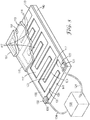
- a sensing element in another embodiment, can be produced that is configured in the general manner of an interdigitated capacitor.
- Exemplary embodiments of interdigitated sensing elements are shown in the top view of Fig. 2 , in the cross-sectional view of Fig. 2a (taken along the line marked "2a" in Fig. 2 ), and in the perspective view of Fig. 3 .
- the term interdigitated encompasses any arrangement comprising at least two electrodes present in an interdigitated configuration.
- Such configurations include interdigitated comb patterns (such as depicted in Figs. 2, 2a and 3 ), as well as interdigitated spiral or serpentine patterns as are well known in the art.
- All of these designs have the common characteristic that (at least) two electrodes are present in a largely coplanar interdigitated arrangement with an analyte-responsive dielectric layer present in proximity to the electrodes such that when an electric field is established between the electrodes, an analyte-responsive dielectric material contained in the layer is capable of interacting with the electric field.
- the analyte-responsive dielectric layer/material may be provided between the electrodes (i.e. in the plane of the two electrodes and interposed in the closest linear path between any two points of approach of the first and second electrodes).
- the analyte-responsive dielectric layer/material may be provided such that, while not coplanar with the electrodes, the analyte-responsive dielectric material is exposed at least to the fringing electric field that is established between adjacent sections of the two electrodes.
- the analyte-responsive dielectric layer may be provided in both locations.
- Interdigitated electrodes can be provided by the deposition of conductive material in two interdigitated patterns by any of the methods (e.g. masked vapor deposition, screenprinting, inkjet printing) that are well known for patterned deposition of materials.
- the particular geometric/dimensional properties of the electrode patterns may be designed as desired.
- interdigitated electrodes are provided on a backing 140 which may be comprised of materials described above.
- First electrode 120 and second electrode 130 are typically provided on the same backing 140.
- first surface 121 of first electrode 120, and first surface 131 of second electrode 130 are both in direct contact with at least some portion of the first surface 141 of backing 140.
- an optional layer or layers can be present between the electrode 120 and/or 130 and the backing 140, similar to the optional layers described above, and subject to the same issues and constraints.
- first electrode 120 and second electrode 130 may leave an area of surface 141 of backing 140, (or, of the surface of any optional layer thereupon) exposed.
- An analyte-responsive dielectric layer can then be deposited onto backing 140, via similar methods to those described above with reference to sensing elements of a parallel-plate type. The deposited analyte-responsive dielectric material will thus fill the spaces between the two electrodes (e.g. spaces 117 depicted in Figs. 2, 2a , and 3 ).
- a first surface 111 of the analyte-responsive dielectric layer 110 will be in direct contact with at least a portion of surface 141 of backing 140.
- the deposition process may also cause the analyte-responsive dielectric layer 110 to cover, and be in contact with, second surface 123 of the first electrode, and second surface 133 of the second electrode, as depicted in Figs. 2a and 3 (unless the deposition is performed selectively, e.g. with one or both of the electrodes masked).
- the first surface 111 of analyte-responsive dielectric layer 110 is in direct contact with second surface 123 of first electrode 120, and/or with second surface 133 of second electrode 130.
- an optional layer (not shown in Figs. 2, 2a , or 3 ) may be provided atop the second surface 123 of first electrode 120, and/or atop the second surface 133 of first electrode 130. (In this embodiment, direct contact between first surface 111 of analyte-responsive dielectric layer 110 and second surface 123 of first electrode 120, and/or second surface 133 of second electrode 130, may not occur).
- Such an optional layer may serve similar purposes (protective, etc.) to those described earlier.
- an optional layer atop one or both electrodes may not necessarily need to be permeable to the analyte since the analyte may not need to penetrate through the an optional layer to reach areas 117 of the analyte-responsive dielectric layer 110.
- an optional cover layer 150 (which may serve as a protective layer, insulating layer, decorative layer, etc.) may be deposited atop the second surface 113 of the analyte-responsive dielectric layer 110. Any such cover layer should not significantly interfere with the functioning of the sensing element (e.g., it should be sufficiently permeable to an analyte of interest).
- This cover layer may comprise a coating deposited by any known coating process (e.g. spin coating, dip coating, solvent coating, vapor coating, transfer coating, screen printing, flexographic printing, and the like).
- cover layer 150 can comprise a premade layer (e.g. a film or tape) that is placed atop second surface 113 of layer 110.
- an electrically accessible area 125 should be provided on first electrode 120, and an accessible area 135 on second electrode 130, to allow electrical contact between each electrode and an operating circuit.
- Such electrically accessible areas can be provided in any convenient location. For example, such electrically accessible areas 125 and 135 are shown on an edge of an electrode in the exemplary illustration of Fig. 2 , and are shown on surfaces 123 and 133 of an electrode in the exemplary illustration of Fig. 3 .
- a connecting device e.g. a contact pad, tab, or the like
- a connecting device 122 may be placed in electrical contact with accessible area 125 of first electrode 120.
- a connecting device 132 may be placed likewise in contact with accessible area 135 of second electrode 130.
- a detectable change in an electrical property associated with the sensing element may occur.
- Such a detectable change may be detected by an operating circuit 28/128 that is in electrical communication with the first and second electrodes.
- "operating circuit” refers generally to an electrical apparatus that can be used to apply a voltage to the first electrode and the second electrode (thus imparting a charge differential to the electrodes), and/or to monitor an electrical property of the sensing element, wherein the electrical property may change in response to the presence of an organic analyte.
- the operating circuit may monitor any or a combination of inductance, capacitance, voltage, resistance, conductance, current, impedance, phase angle, loss factor, or dissipation.
- Such an operating circuit may comprise a single apparatus which both applies voltage to the electrodes, and monitors an electrical property. In an alternative embodiment, such an operating circuit may comprise two separate apparatuses, one to provide voltage, and one to monitor the signal.
- An operating circuit may be connected to first electrode 20/120 and to second electrode 30/130 by wires 24/124 and 34/134.
- an operating circuit may be provided in direct contact with the first and/or the second electrode, either via connecting devices 22/122 and 32/132, or by contacting some portion of the operating circuit directly to an electrically accessible area of each electrode.
- an operating circuit can be provided that resides on a circuit board or a flexible circuit (either of which can also serve as backing 40/140). A first electrode can then be deposited directly onto circuit board/backing 40 such that it is in direct contact with a portion of the operating circuit.
- An operating circuit 28/128 may include, for example, a power supply (which may comprise a battery or a hardwired power source; alternatively, power may be provided indirectly via, for example, charging of an RFID circuit that is built into the operating circuit).
- An operating circuit 28/128 may also include one or more microprocessors configured to control the charging of the electrodes and/or to monitor changes in one or more electrical properties of a charged sensing electrode pair. Also present may be analog-to-digital converters, memory devices for storing data derived from the sensing element, software for operating the sensing element, components that provide data logging and/or one-or two-way telemetry capability, and so on.
- a sensing element such as herein disclosed can be used to detect and/or monitor (whether qualitatively or quantitatively) the presence of an organic analyte or analytes.
- analytes can include, but are not limited to, hydrocarbons, fluorocarbons, alkanes, cycloalkanes, aromatic compounds, alcohols, ethers, esters, ketones, halocarbons, amines, organic acids, cyanates, nitrates, and nitriles, for example n-octane, cyclohexane, methyl ethyl ketone, acetone, ethyl acetate, carbon disulfide, carbon tetrachloride, benzene, styrene, toluene, xylenes, methyl chloroform, tetrahydrofuran, methanol, ethanol, isopropyl alcohol, n-butyl alcohol, t-butyl alcohol, 2-
- Analytes can be relatively nonpolar organic molecules or relatively polar organic molecules.
- Analytes can be so-called vapors; i.e. molecules that are capable of forming a solid or liquid under the ambient conditions of temperature and pressure that the analyte is experiencing (e.g. toluene, acetone, heptane, etc.).
- Analytes can be so-called gases; i.e. molecules that are not normally capable of forming a liquid or solid under ambient conditions (although such molecules may still comprise a more highly condensed state in the internal pores of the analyte-responsive dielectric material, as discussed above). Such gases may include methane, ethane, and the like. Mixtures of organic analyte molecules may in some circumstances be detected.
- PIM material was prepared from the monomers 5,5',6,6'-tetrahydroxy-3,3,3',3'-tetramethyl-1,1'-spirobisindane and tetrafluoroterephthalonitrile generally according to the procedure reported by Budd et al. in Advanced Materials, 2004, Vol. 16, No. 5, pp. 456-459 .
- PIM material was prepared following the same general procedure described for PIM 1. 19.31 grams of 5,5',6,6'-tetrahydroxy-3,3,3',3'-tetramethyl-1,1'-spirobisindane were combined with 11.34 g of tetrafluoroterephthalonitrile, 47.02 g potassium carbonate, and 500 milliliters of N,N-dimethylformamide, and the mixture was reacted at 65°C for 48 hours. The resulting polymer was dissolved in tetrahydrofuran, precipitated three times from methanol, and then dried under vacuum at room temperature. A yellow solid product was obtained having a weight-average molecular weight of approximately 109,000 and a number-average molecular weight of approximately 73,600, as determined by gel permeation chromatography analysis using light scattering detection.
- PIM material was prepared following the same general procedure described for PIM 1. 5.62 grams of 5,5',6,6'-tetrahydroxy-3,3,3',3'-tetramethyl-1,1'-spirobisindane were combined with 3.30 g of tetrafluoroterephthalonitrile, 13.68 g potassium carbonate, and 150 milliliters of N,N-dimethylformamide, and the mixture was reacted at 65°C for 62 hours. The resulting polymer was dissolved in tetrahydrofuran, precipitated two times from methanol, and then dried under vacuum at room temperature. A yellow solid product was obtained having a weight-average molecular weight of approximately 65,300 and a number-average molecular weight of approximately 35,600, as determined by gel permeation chromatography analysis using light scattering detection.
- PIM material was prepared following the same general procedure described for PIM 1 except using recrystallized 5,5',6,6'-tetrahydroxy-3,3,3',3'-tetramethyl-1,1'-spirobisindane.
- 5,5',6,6'-tetrahydroxy-3,3,3',3'-tetramethyl-1,1'-spirobisindane purchased from Aldrich was recrystallized from THF/heptane (1.2:1) prior to use in polymerization.
- a cleaned piece of glass (2.5 cm by 2.5 cm) was coated with a continuous (unpatterned) coating of aluminum using a CHA Industries Mark-50 evaporator operated at a base pressure of 1x10 -5 torr and No. A-2049 aluminum pellets (99.995 % purity, 6X6 mm, from Cerac Inc.).
- the aluminum coating was deposited at a rate of 15 angstroms/second. The final thickness was 100 nm.
- a diamond-tipped pen was used to score the aluminized glass approximately 5 mm from one edge. The scored piece of aluminized glass was taped down to a 5 cm by 5 cm piece of glass such that there was a margin of masked aluminum surface all around the edge of the sample.
- a 4 weight % solution of PIM 1 in chlorobenzene was prepared and spin coated onto the masked sample at 1200 rpm for 2 minutes using a WS-400B-8NPP-Lite Single Wafer spin processor manufactured by Laurell Technologies, Corp. North Wales, PA.
- a second electrode was made using a silver nanoparticle suspension (30 nm mean particle diameter, suspended in methanol) available under the designation Silverjet DGP-40LT-25C from Advanced Nano Products Co., Ltd. (South Korea). A 0.5 g quantity of this as-received suspension was mixed with 1 milliliter of methanol.
- the diluted silver nanoparticle suspension was spin coated onto the PIM film at 1000 rpm for 2 minutes.
- the tape was removed from the masked sample, and the sample was heated in a conventional drying oven for 3 hours at 150°C.
- a premade mask By attaching a premade mask to the sample, a series of 1 mm wide by 4 mm long aluminum tabs were made on the sample on the side nearest the score line such that the aluminum tabs connected the second electrode to the bottom aluminum electrode.
- Aluminum evaporation was carried out in a Kurt Lesker vacuum system at a base pressure of 1 X 10 -6 torr.
- the final thickness was 100 nm.
- This procedure thus provided a glass (backing) layer with a first electrode comprising continuous aluminum, to which an operating circuit could be contacted.
- Atop the aluminum electrode was an analyte-responsive dielectric layer comprising a PIM material (approximately 600 nm thick).
- Atop the PIM material was a second electrode comprising a microscopically-discontinuous (thus analyte-permeable) silver layer (approximately 300 nm thick). This second electrode was in contact with the smaller aluminum-coated area via aluminum tabs, such that the second electrode could be connected with the operating circuit by attaching the circuit to the smaller aluminum-coated area.
- a cleaned piece of glass was coated with aluminum, scored, masked and coated with PIM 1 as described for Sample 1.
- the tape was removed from the masked sample, and the sample was heated in a conventional drying oven for 1 hour at 150°C.
- a patterned second electrode was inkjet printed on top of the PIM material to complete the construction of this sample.
- a bitmap image (702 dots per inch) was created in Adobe Photoshop and then downloaded to an XY deposition system.
- the printhead used for depositing the silver was a Dimatix SX3-128 printhead with a 10 pL drop volume and 128 jets/orifices, the printhead assembly being approximately 6.5 cm long with 508 micron jet to jet spacing.
- the silver nanoparticle sol used to construct this electrode was obtained from Cabot under the designation AG-IJ-G-100-S1. This silver nanoparticle sol was approximately 15-40 wt % ethanol, 15-40 wt % ethylene glycol, and 20 wt % silver.
- the sample was held securely during the inkjet printing process by use of a porous aluminum vacuum platen. Upon completion of printing, the sample was removed from the porous aluminum vacuum platen and placed on a Thermolyne hot plate for 15 minutes at 125°C.
- the inkjet printed silver electrode comprised a comb pattern that consisted of a solid rectangle with lines extending from one edge.
- the rectangular portion of the printed electrode was positioned such that a portion of the rectangle was atop a portion of the smaller aluminum-coated area (such that electrical contact with the top electrode could be achieved by attaching a wire to the smaller aluminum-coated area), with the remainder of the second printed electrode being atop the PIM material.
- the lines on the electrode were designed to be approximately 8.3 mm long and approximately 102 microns wide.
- the gap between the lines was designed to be approximately 152 microns. (It should be noted that all of these dimensions were the nominal dimensions of the bitmap image and not the actual 'printed' dimensions).
- This procedure provided a glass backing layer with a first electrode comprising continuous aluminum. Atop the aluminum electrode was an analyte-responsive dielectric layer comprising a PIM material, with a second electrode comprising a silver layer in a comb pattern residing atop the PIM layer. An operating circuit could be attached to the electrodes in similar manner to that described with reference to Sample 1.
- An interdigitated electrode transducer was fabricated by vapor depositing copper (at a thickness of approximately 43 microns) onto a polyimide backing layer (of thickness approximately 52 microns).
- the electrodes comprised interdigitated comb patterns of 0.5 cm by 0.5 cm in dimension connected to conductive leads.
- the electrode lines had a width of approximately 20 microns and a pitch of approximately 40 microns.
- the interdigitated transducer was taped down to a 5 cm by 5 cm piece of glass such that two ends of the transducer were covered with tape with one of the pieces of tape completely covering the conductive leads.
- a 4 weight % solution of PIM 1 (prepared as described above) in chlorobenzene was spin coated onto the masked sample at 2500 rpm for 2 minutes.
- the tape was removed from the masked sample. This procedure thus provided a polyimide backing layer bearing first and second interdigitated copper electrodes. Atop the interdigitated electrodes was an analyte-responsive dielectric layer comprising a PIM material of approximately 400 nm thickness.
- An interdigitated electrode transducer was fabricated by vapor depositing gold onto a polymeric backing layer. The gold was then photolithographically defined to comprise interdigitated comb patterns of 1.2 cm by 1.0 cm in dimension connected to conductive leads. The electrode lines had a pitch of approximately 320 microns.
- the interdigitated transducer was taped down to a 5 cm by 5 cm piece of glass such that two ends of the transducer were covered with tape with one of the pieces of tape completely covering the conductive leads.
- a 4 weight % solution of PIM 2 (prepared as described above) in chlorobenzene was spin coated onto the masked sample at 1200 rpm for 2 minutes.
- the tape was removed from the masked sample, and the sample was heated in a conventional drying oven for 1 hour at 100°C. This procedure thus provided a polymeric backing layer bearing first and second interdigitated gold electrodes. Atop the interdigitated electrodes was an analyte-responsive dielectric layer comprising a PIM material of approximately 400 nm thickness.
- An interdigitated electrode transducer was fabricated by vapor depositing gold onto a polymeric backing layer. The gold was then photolithographically defined to comprise interdigitated comb patterns of 1.2 cm by 1.0 cm in dimension connected to conductive leads. The electrode lines had a pitch of approximately 120 microns.
- the interdigitated transducer was taped down to a 5 cm by 5 cm piece of glass such that two ends of the transducer were covered with tape with one of the pieces of tape completely covering the conductive leads.
- a 4 weight % solution of PIM 2 (prepared as described above) in chlorobenzene was spin coated onto the masked sample at 1200 rpm for 2 minutes. The tape was removed from the masked sample, and the sample was heated in a conventional drying oven for 1 hour at 100°C. This procedure thus provided a polymeric backing layer bearing first and second interdigitated gold electrodes. Atop the interdigitated electrodes was an analyte-responsive dielectric layer comprising a PIM material of approximately 400 nm thickness.
- An interdigitated electrode transducer was fabricated by vapor depositing gold onto a polymeric backing layer. The gold was then photolithographically defined to comprise interdigitated comb patterns of 1.2 cm by 1.0 cm in dimension connected to conductive leads. The electrode lines had a pitch of approximately 80 microns.
- the interdigitated transducer was taped down to a 5 cm by 5 cm piece of glass such that two ends of the transducer were covered with tape with one of the pieces of tape completely covering the conductive leads.
- a 4 weight % solution of PIM 2 (prepared as described above) in chlorobenzene was spin coated onto the masked sample at 1200 rpm for 2 minutes. The tape was removed from the masked sample, and the sample was heated in a conventional drying oven for 1 hour at 100°C. This procedure thus provided a polymeric backing layer bearing first and second interdigitated gold electrodes. Atop the interdigitated electrodes was an analyte-responsive dielectric layer comprising a PIM material of approximately 400 nm thickness.
- An interdigitated electrode transducer was fabricated by vapor depositing gold onto a polymeric backing layer. The gold was then photolithographically defined to comprise interdigitated comb patterns of 1.2 cm by 1.0 cm in dimension connected to conductive leads. The electrode lines had a pitch of approximately 40 microns.
- the interdigitated transducer was taped down to a 5 cm by 5 cm piece of glass such that two ends of the transducer were covered with tape with one of the pieces of tape completely covering the conductive leads.
- a 4 weight % solution of PIM 2 (prepared as described above) in chlorobenzene was spin coated onto the masked sample at 1200 rpm for 2 minutes. The tape was removed from the masked sample, and the sample was heated in a conventional drying oven for 1 hour at 100°C. This procedure thus provided a polymeric backing layer bearing first and second interdigitated gold electrodes. Atop the interdigitated electrodes was an analyte-responsive dielectric layer comprising a PIM material of approximately 400 nm thickness.
- a gold-coated poly(ethylene terephthalate) (PET) (ST504, E. I. DuPont de Nemours and Company, Wilmington, Delaware) substrate was prepared by thermal evaporation (DV-502A, Denton Vacuum, Moorestown, New Jersey) of 20 angstroms of chromium followed by 100 nm of gold.
- PET poly(ethylene terephthalate)
- DV-502A Denton Vacuum, Moorestown, New Jersey
- the master tool used for molding an elastomeric stamp was generated by preparing patterns of photoresist (Shipley1818, Rohm and Haas Company, Philadelphia, Pennsylvania) on a 10 cm diameter silicon wafer using photolithography.
- the elastomeric stamp was molded against the master tool by pouring uncured poly(dimethylsiloxane) (PDMS, SylgardTM 184, Dow Corning, Midland Michigan) over the tool to a thickness of approximately 3.0 mm.
- PDMS poly(dimethylsiloxane)
- SylgardTM 184 Dow Corning, Midland Michigan
- the uncured silicone in contact with the master was degassed by exposing to a vacuum and then cured for 2 hours at 70°C.
- a PDMS stamp was provided with a relief pattern comprising raised features approximately 1.8 microns in height. With this stamp, interdigitated electrode transducers having electrode lines with a width of approximately 3 microns and a pitch of approximately 10 microns were produced.
- the structured stamp was inked by contacting its back side (flat surface without relief pattern) with a solution of 10 mM octadecylthiol ("ODT" 00005, TCI AMERICA, Wellesley Hills, Massachusetts) in ethanol for 20 hours.
- ODT octadecylthiol
- the gold coated PET film was contacted to the stamp relief patterned surface, which was face up, by first contacting an edge of the film sample to the stamp surface and then rolling the film into contact across the stamp using a roller with a diameter of approximately 3.0 cm.
- the gold coated PET film was then left in contact with the stamp for 20 seconds thereby placing a patterned self-assembled monolayer (SAM) of thiols on the gold surface.
- SAM self-assembled monolayer
- the gold coated PET film was then peeled from the stamp.
- the gold coated PET film with printed pattern was then immersed into an etchant solution for 50 seconds for selective etching and metal patterning.
- the etchant comprised 1.0 grams of thiourea (T8656, Sigma-Aldrich, St. Louis, Missouri), 0.54 milliliters of concentrated hydrochloric acid (HX0603-75, EMD Chemicals, Gibbstown, New Jersey), 0.5 milliliters of hydrogen peroxide (30%, 5240-05, Mallinckrodt Baker, Phillipsburg, New Jersey), and 21 grams of deionized water.
- the tape was removed from the masked sample, and the sample was heated in a conventional drying oven for 1 hour at 100°C. This procedure thus provided a polymeric backing layer bearing first and second interdigitated gold electrodes. Atop the interdigitated electrodes was an analyte-responsive dielectric layer comprising a PIM material of approximately 400 nm thickness.
- a 1.2 cm by 2.0 cm corner of a cleaned piece of glass (2.5 cm by 2.5 cm) was evaporatively coated with a continuous (unpatterned) coating of first 10 nm of titanium followed by 100 nm of aluminum using the equipment described above in the Preparation of Sample 1.
- a chlorobenzene solution of PIM 3 was used to spin coat a 750 nm thick layer on top of the entire glass piece.
- a swab with a small amount of acetone was used to remove the PIM layer to expose a small corner of the bottom aluminum electrode for connection to an operating circuit.
- a 0.9 cm by 1.5 cm rectangle of a silver nanoparticle sol (Cabot AG-IJ-G-100-S1) was printed on top of the PIM layer positioned such that only a 0.9 cm by 1.0 cm portion of the rectangle was directly over the bottom aluminum electrode.
- the sample was placed on a Thermolyne hot plate for 15 minutes at 125°C.
- the top inkjet printed electrode was thickened (only in the area that was not directly over the bottom aluminum electrode) using the Advanced Nano Products Co., Ltd. silver nanoparticle suspension (Silverjet DGP-40LT-25C from Advanced Nano Products Co., Ltd.).
- This thickening step was accomplished by simply using a paint brush to brush the nanoparticle suspension on top of the desired area. After the thickening step, the sample was dried in a conventional drying oven for 1 hour at 150°C. This procedure provided a glass backing layer with a first electrode comprising continuous aluminum. Atop the aluminum electrode was an analyte-responsive dielectric layer comprising a PIM material, with a second electrode comprising a microscopically-discontinuous (thus analyte-permeable) silver layer residing atop the PIM layer. An operating circuit could be attached to the electrodes in similar manner to that described with reference to Sample 1.
- a 1.2 cm by 2.0 cm corner of a cleaned piece of glass (2.5 cm by 2.5 cm) was evaporatively coated with a continuous (unpatterned) coating of first 10 nm of titanium followed by 100 nm of aluminum using the equipment described above in the Preparation of Sample 1.
- a chlorobenzene solution of PIM 4 was used to spin coat a 400 nm thick layer on top of the entire glass piece.
- a swab with a small amount of acetone was used to remove the PIM layer to expose a small corner of the bottom aluminum electrode for connection to an operating circuit.
- a 0.9 cm by 1.5 cm rectangle of a silver nanoparticle sol (Cabot AG-IJ-G-100-S1) was printed on top of the PIM layer positioned such that only a 0.9 cm by 1.0 cm portion of the rectangle was directly over the bottom aluminum electrode.
- the sample was placed on a Thermolyne hot plate for 15 minutes at 125°C.
- the top inkjet printed electrode was thickened (only in the area that was not directly over the bottom aluminum electrode) using the Advanced Nano Products Co., Ltd. silver nanoparticle suspension (Silverjet DGP-40LT-25C from Advanced Nano Products Co., Ltd.).
- This thickening step was accomplished by simply using a paint brush to brush the nanoparticle suspension on top of the desired area. After the thickening step, the sample was dried in a conventional drying oven for 1 hour at 150°C. This procedure provided a glass backing layer with a first electrode comprising continuous aluminum. Atop the aluminum electrode was an analyte-responsive dielectric layer comprising a PIM material, with a second electrode comprising a microscopically-discontinuous (thus analyte-permeable) silver layer residing atop the PIM layer. An operating circuit could be attached to the electrodes in similar manner to that described with reference to Sample 1.
- a simple flow-through custom built delivery system was used to deliver known concentrations of acetone to the sample for measurement. Teflon tubing was used throughout the delivery system. Nitrogen was sparged through a container that contained acetone in liquid form and held at a constant temperature as to provide a nitrogen stream that was saturated with acetone. The liquid acetone was kept at a constant temperature using a chiller from Fisher Scientific, and the temperature at which to keep the chiller in order to create a saturated gaseous stream of acetone was calculated using the Handbook of Vapor Pressure (Yaws, C.I. Gulf Publishing: Houston, 1994 ). The saturated gaseous acetone stream was diluted with additional nitrogen by use of a series of mass flow controllers.
- the concentration of acetone in the gaseous stream was calibrated by use of an infrared spectrometer (available under the designation Miran Sapphire from ThermoElectron of Waltham, MA).
- the gaseous acetone stream was introduced into a sample chamber (held at controlled temperature) containing Sample 1.
- the first and second electrodes of the sample were connected to an operating circuit that comprised an LCR meter (available under the designation Instek Model 821 LCR meter from Instek America, Corp. Chino, CA) using alligator clips.
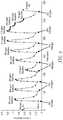
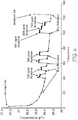
- the changes in capacitance (in nanoFarads) of the sample were monitored at a frequency of 10 kilohertz at specific time intervals during the entire course of the vapor test (as shown in Fig. 4 ).
- the acetone concentration was reduced step-wise to 651 ppm, then to 394 ppm, then to 133 ppm. Thereafter, the sample was exposed to dry nitrogen. The test chamber was then opened, and the sample was exposed to ambient conditions (air, 51 % relative humidity).
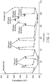
- Sample 2 (prepared as described above) was tested using the same set-up described with reference to Sample 1.
- the changes in capacitance (in nanoFarads) of the sample were monitored at a frequency of 10 kilohertz at specific time intervals during the entire course of the vapor test (as shown in Fig. 5 ).
- the sample was placed in the unsealed test chamber in order to measure the initial capacitance of the sample at ambient room conditions (air, approximately 64% relative humidity).
- the sample was then exposed to dry nitrogen (approximately 8% relative humidity, 20°C).
- the test chamber was sealed and a dry nitrogen stream containing 394 ppm of acetone was introduced into the test chamber. Then, the test chamber was returned to a dry nitrogen environment.
- the exposure to 394 ppm of acetone was repeated two more times, each time followed by exposure to dry nitrogen. Thereafter, the sample was exposed to successive nitrogen streams containing 133, 394, 651 and 915 ppm, with the sample being returned to an acetone-free dry nitrogen environment in between each exposure. After the last dry nitrogen exposure, the sample was exposed to a dry nitrogen stream with 915 ppm of acetone. After a period of time, the acetone concentration was reduced step-wise to 651 ppm, then to 394 ppm, then to 133 ppm. Thereafter, the sample was exposed to dry nitrogen. The test chamber was then opened, and the sample was exposed to ambient conditions (air, 64% relative humidity).
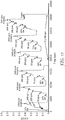
- Sample 3 (prepared as described above) was tested using the same set-up as described with reference to Sample 1.
- the changes in capacitance (in picoFarads) of the sample were monitored at a frequency of 20 kilohertz at specific time intervals during the test (as shown in Fig. 6 ).
- the sample was placed in the unsealed test chamber in order to measure the initial capacitance of the sample at ambient room conditions (air, 40% relative humidity, not shown in Fig. 6 ).
- the sample was then exposed to dry nitrogen (8% relative humidity, 20°C).
- the test chamber was sealed and a dry nitrogen stream containing 133 ppm of acetone was introduced into the test chamber (in Fig.
- the peak in between the dry nitrogen exposure and the 133 ppm acetone exposure is an artifact).
- the concentration of acetone was increased to 394 ppm.
- the concentration of acetone was increased to 651 ppm.
- the concentration of acetone was increased to 915 ppm.
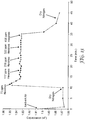
- Sample 4 (prepared as described above) was tested using the same set-up as described with reference to Sample 1.
- the changes in capacitance (in picoFarads) of the sample were monitored at a frequency of 10 kilohertz at specific time intervals during the test (as shown in Fig. 7 ).
- the sample was placed in the unsealed test chamber in order to measure the initial capacitance of the sample at ambient room conditions (air, approximately 50% relative humidity).
- the test chamber was sealed and, the sample was then exposed to dry nitrogen (approximately 8% relative humidity, 20°C). A dry nitrogen stream containing 133 ppm of acetone was then introduced into the test chamber. Then, the test chamber was returned to a dry nitrogen environment.
- the exposure to 133 ppm of acetone was repeated followed by exposure to dry nitrogen.
- a dry nitrogen stream containing 394 ppm of acetone was then introduced into the test chamber.
- the test chamber was then returned to a dry nitrogen environment.
- the exposure to 394 ppm of acetone was repeated followed by exposure to dry nitrogen.
- the sample was then exposed to a dry nitrogen stream with 651 ppm of acetone.
- the acetone concentration was reduced step-wise to 394 ppm and then to 133 ppm. Thereafter, the sample was exposed to dry nitrogen.
- Sample 5 (prepared as described above) was tested using the same set-up as described with reference to Sample 1.
- the changes in capacitance (in picoFarads) of the sample were monitored at a frequency of 10 kilohertz at specific time intervals during the test (as shown in Fig. 8 ).
- the sample was placed in the unsealed test chamber in order to measure the initial capacitance of the sample at ambient room conditions (air, approximately 52% relative humidity).
- the chamber was sealed and, the sample was then exposed to dry nitrogen (approximately 8% relative humidity, 20°C).
- a dry nitrogen stream containing 133 ppm of acetone was then introduced into the test chamber. Then, the test chamber was returned to a dry nitrogen environment.
- the exposure to 133 ppm of acetone was repeated followed by exposure to dry nitrogen.
- a dry nitrogen stream containing 394 ppm of acetone was then introduced into the test chamber.
- the test chamber was then returned to a dry nitrogen environment.
- the exposure to 394 ppm of acetone was repeated followed by exposure to dry nitrogen.
- the sample was then exposed to a dry nitrogen stream with 651 ppm of acetone.
- the acetone concentration was reduced step-wise to 394 ppm and then to 133 ppm. Thereafter, the sample was exposed to dry nitrogen.
- the test chamber was then opened, and the sample was exposed to ambient conditions (air, 50% relative humidity).
- Sample 6 (prepared as described above) was tested using the same set-up as described with reference to Sample 1.
- the changes in capacitance (in picoFarads) of the sample were monitored at a frequency of 10 kilohertz at specific time intervals during the test (as shown in Fig. 9 ).
- the sample was placed in the unsealed test chamber in order to measure the initial capacitance of the sample at ambient room conditions (air, approximately 71 % relative humidity).
- the test chamber was sealed and, the sample was then exposed to dry nitrogen (approximately 8% relative humidity, 20°C).
- a dry nitrogen stream containing 133 ppm of acetone was then introduced into the test chamber. Then, the test chamber was returned to a dry nitrogen environment.
- the exposure to 133 ppm of acetone was repeated followed by exposure to dry nitrogen.
- a dry nitrogen stream containing 394 ppm of acetone was then introduced into the test chamber.
- the test chamber was then returned to a dry nitrogen environment.
- the exposure to 394 ppm of acetone was repeated followed by exposure to dry nitrogen.
- the sample was then exposed to a dry nitrogen stream with 651 ppm of acetone.
- the acetone concentration was reduced step-wise to 394 ppm and then to 133 ppm. Thereafter, the sample was exposed to dry nitrogen.
- the test chamber was then opened, and the sample was exposed to ambient conditions (air, 71 % relative humidity).
- Sample 7 (prepared as described above) was tested using the same set-up as described with reference to Sample 1.
- the changes in capacitance (in picoFarads) of the sample were monitored at a frequency of 10 kilohertz at specific time intervals during the test (as shown in Fig. 10 ).
- the sample was placed in the unsealed test chamber in order to measure the initial capacitance of the sample at ambient room conditions (air, approximately 74% relative humidity).
- the test chamber was sealed and, the sample was then exposed to dry nitrogen (approximately 8% relative humidity, 20°C).
- a dry nitrogen stream containing 133 ppm of acetone was then introduced into the test chamber. Then, the test chamber was returned to a dry nitrogen environment.
- the exposure to 133 ppm of acetone was repeated followed by exposure to dry nitrogen.
- a dry nitrogen stream containing 394 ppm of acetone was then introduced into the test chamber.
- the test chamber was then returned to a dry nitrogen environment.
- the exposure to 394 ppm of acetone was repeated followed by exposure to dry nitrogen.
- the sample was then exposed to a dry nitrogen stream with 651 ppm of acetone.
- the acetone concentration was reduced step-wise to 394 ppm and then to 133 ppm. Thereafter, the sample was exposed to dry nitrogen.
- the test chamber was then opened, and the sample was exposed to ambient conditions (air, 71 % relative humidity).
- Sample 8 (prepared as described above) was tested using the same set-up as described with reference to Sample 1.
- the changes in capacitance (in picoFarads) of the sample were monitored at a frequency of 200 kilohertz at specific time intervals during the test (as shown in Fig. 11 ).
- the sample was placed in the unsealed test chamber in order to measure the initial capacitance of the sample at ambient room conditions (air, approximately 66% relative humidity).
- the test chamber was sealed and, the sample was then exposed to dry nitrogen (approximately 8% relative humidity, 20°C).
- a dry nitrogen stream containing 133 ppm of acetone was then introduced into the test chamber. Then, the test chamber was returned to a dry nitrogen environment.
- the exposure to 133 ppm of acetone was repeated followed by exposure to dry nitrogen.
- a dry nitrogen stream containing 394 ppm of acetone was then introduced into the test chamber.
- the test chamber was then returned to a dry nitrogen environment.
- the exposure to 394 ppm of acetone was repeated followed by exposure to dry nitrogen.
- the sample was then exposed to a dry nitrogen stream with 133 ppm of acetone.
- the acetone concentration was increased step-wise to 394 ppm and then to 651 ppm.
- the acetone concentration was reduced step-wise to 394 ppm and then to 133 ppm.
- the sample was exposed to dry nitrogen.
- the test chamber was then opened, and the sample was exposed to ambient conditions (air, 65% relative humidity).
- Sample 9 (prepared as described above) was tested using the same set-up as described with reference to Sample 1.
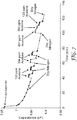
- the changes in capacitance (in nanoFarads) of the sample were monitored at a frequency of 1 kilohertz at specific time intervals during the test.
- the data is plotted in Fig. 12 as a change of capacitance ratio ( ⁇ C/C o ) over time (as opposed to the absolute capacitance).
- the sample was placed in the test chamber, and the test chamber was sealed.
- the sample was then exposed to dry nitrogen (approximately 8% relative humidity, 20°C; not shown in Fig. 12 ).
- the capacitance of the sample under these dry nitrogen conditions was used as the C 0 value throughout the experiment.
- the entire experiment was performed at a fixed temperature of 20°C and thus the relative humidity values were calculated at that temperature.
- the sample was then exposed to a nitrogen stream containing 12% relative humidity. After a period of time, the sample was exposed to a nitrogen stream containing 12% relative humidity and 50 ppm of acetone. Keeping the relative humidity fixed at 12%, the acetone concentration was increased sequentually to 250, 500 and 1000 ppm.
- the test chamber was then returned to the 12% relative humidity nitrogen environment. After a period of time, the relative humidity in the nitrogen stream was increased to 24%.
- the sample was then exposed sequentially to increasing concentrations of acetone (50, 250, 500 and 1000 ppm) at a fixed relative humidity of 24%.
- the test chamber was then returned to the 24% relative humidity nitrogen environment. After a period of time, the relative humidity in the nitrogen stream was increased to 39%. The sample was then exposed sequentially to increasing concentrations of acetone (50, 250, 500 and 1000 ppm) at a fixed relative humidity of 39%. The test chamber was then returned to the 39% relative humidity nitrogen environment. The test chamber was then returned to a dry nitrogen environment (8% relative humidity). After a period of time, the relative humidity in the nitrogen stream was increased to 56%. The sample was then exposed sequentially to increasing concentrations of acetone (50, 250, 500 and 1000 ppm) at a fixed relative humidity of 56%. The test chamber was then returned to the 56% relative humidity nitrogen environment.
- the relative humidity in the nitrogen stream was increased to 70%.
- the sample was then exposed sequentially to increasing concentrations of acetone (50, 250, 500 and 1000 ppm) at a fixed relative humidity of 70%.
- the test chamber was then returned to the 70% relative humidity nitrogen environment.
- the relative humidity in the nitrogen stream was increased to 88%.
- the sample was then exposed sequentially to increasing concentrations of acetone (50, 250, 500 and 1000 ppm) at a fixed relative humidity of 88%.
- the sample was then exposed to a gaseous stream containing 0 ppm acetone, at 88% relative humidity.
- the sample was then returned to a dry nitrogen environment (8% relative humidity).
- Sample 10 (prepared as described above) was tested using the same set-up as described with reference to Sample 1.
- the changes in capacitance (in nanoFarads) of the sample were monitored at a frequency of 1 kilohertz at specific time intervals during the test.
- the data is plotted in Figure 13 as a change of capacitance ratio ( ⁇ C/C o ) over time.
- the sample was placed in the test chamber, and the test chamber was sealed.
- the sample was then exposed to dry nitrogen (approximately 8% relative humidity, 20°C).
- the capacitance of the sample under these dry nitrogen conditions was used as the C 0 value throughout the experiment.
- a dry nitrogen stream containing 5 ppm of acetone was introduced into the test chamber. Then, the test chamber was returned to a dry nitrogen environment.
- the sample was then exposed to a dry nitrogen stream containing 10 ppm of acetone. After a period of time, the acetone concentration was increased to 20 ppm. Thereafter, the sample was exposed to successive nitrogen streams containing 50, 100, 200 and 500 ppm of acetone. The sample was then returned to a dry nitrogen environment. (In Fig. 13 , the drop in capacitance ratio between the 200 and 500 ppm acetone exposures is an artifact caused by an issue in the delivery of the analyte.)
- the changes in capacitance (in nanoFarads) of the sample were monitored at a frequency of 1 kilohertz at specific time intervals during the test (as shown in Fig. 14 ).
- the sample was placed in the unsealed test chamber in order to measure the initial capacitance of the sample at ambient room conditions (air, approximately 29% relative humidity).
- the test chamber was sealed, and the sample was exposed to dry nitrogen (approximately 8% relative humidity, 20°C).
- a dry nitrogen stream containing 16 ppm of toluene was then introduced into the test chamber.
- the toluene concentration was increased to 26 ppm. Thereafter, the sample was exposed to successive nitrogen streams containing 48, 91 and 175 ppm of toluene. The sample was then returned to a dry nitrogen environment.
- the changes in capacitance (in nanoFarads) of the sample were monitored at a frequency of 1 kilohertz at specific time intervals during the test (as shown in Fig. 15 ).
- the sample was placed in the unsealed test chamber in order to measure the initial capacitance of the sample at ambient room conditions (air, approximately 23% relative humidity).
- the chamber was sealed, and the sample was then exposed to dry nitrogen (approximately 8% relative humidity, 20°C).
- a dry nitrogen stream containing 73 ppm of hexanes was then introduced into the test chamber.
- the hexanes concentration was increased to 117 ppm. Thereafter, the sample was exposed to successive nitrogen streams containing 231, 322 and 408 ppm of hexanes. The sample was then returned to a dry nitrogen environment.
- the changes in capacitance (in nanoFarads) of the sample were monitored at a frequency of 1 kilohertz at specific time intervals during the test (as shown in Fig. 16 ).
- the sample was placed in the unsealed test chamber in order to measure the initial capacitance of the sample at ambient room conditions (air, approximately 23% relative humidity).
- the test chamber was sealed, and the sample was then exposed to dry nitrogen (approximately 8% relative humidity, 20°C).
- a dry nitrogen stream containing 45 ppm of isopropyl alcohol (IPA) was introduced into the test chamber. Then, the test chamber was returned to a dry nitrogen environment. The sample was then exposed to a dry nitrogen stream containing 15 ppm of IPA. After a period of time, the IPA concentration was increased to 23 ppm. Thereafter, the sample was exposed to successive nitrogen streams containing 45, 87, 171 and 254 ppm of IPA. The sample was then returned to a dry nitrogen environment. The test chamber was then opened, and the sample was exposed to ambient conditions (air, 26% relative humidity).
- ambient conditions air, 26% relative humidity
Claims (13)
- Élément de détection (1 ; 101) pour détecter un analyte chimique organique, comprenant :une première électrode (20 ; 120) et une deuxième électrode (30 ; 130) ; et,un matériau diélectrique microporeux hydrophobe sensible à un analyte (10 ; 110) disposé au moins à proximité des première et deuxième électrodes, dans lequel le matériau diélectrique microporeux hydrophobe sensible à un analyte est un polymère de microporosité intrinsèque ; caractérisé en ce que le polymère de microporosité intrinsèque comprend des macromolécules organiques constituées d'espèces généralement planes reliées par des lieurs rigides, lesdits lieurs rigides possédant un point de contorsion de telle sorte que deux espèces planes adjacentes reliées par le lieur sont maintenues dans une orientation non coplanaire.
- Élément de détection selon la revendication 1, dans lequel le polymère de microporosité intrinsèque comprend des macromolécules organiques constituées de premières espèces généralement planes reliées par des lieurs rigides principalement à un maximum de deux autres premières espèces précitées, lesdits lieurs rigides possédant un point de contorsion de telle sorte que deux premières espèces planes adjacentes reliées par le lieur sont maintenues dans une orientation non coplanaire.
- Élément de détection selon la revendication 1, dans lequel le point de contorsion est un groupe spiro, un fragment de cycle ponté ou une liaison covalente simple stériquement encombrée autour de laquelle il y a une rotation limitée.
- Élément de détection selon la revendication 1, dans lequel au moins une des électrodes est perméable à un analyte chimique organique.
- Élément de détection selon la revendication 1, dans lequel l'élément de détection comprend une configuration de condensateur à plaques parallèles.
- Élément de détection selon la revendication 1, dans lequel l'élément de détection comprend une configuration de condensateur interdigitée.
- Élément de détection selon la revendication 1, où l'élément de détection comprend une couche de couverture à proximité d'au moins une des électrodes.
- Élément de détection selon la revendication 7, dans lequel la couche de couverture est perméable à un analyte chimique organique.
- Capteur pour détecter un analyte chimique organique, comprenant :un élément de détection (1 ; 101) selon la revendication 1 ;
et,un circuit de commande (28 ; 128) en communication électrique avec les première et deuxième électrodes, dans lequel le circuit de commande est susceptible d'appliquer une tension aux première et deuxième électrodes et est susceptible de détecter un changement dans une propriété électrique de l'élément de détection. - Capteur selon la revendication 9, dans lequel le polymère de microporosité intrinsèque comprend des macromolécules organiques constituées de premières espèces généralement planes reliées par des lieurs rigides principalement à un maximum de deux autres premières espèces précitées, lesdits lieurs rigides possédant un point de contorsion de telle sorte que deux premières espèces planes adjacentes reliées par le lieur sont maintenues dans une orientation non coplanaire.
- Capteur selon la revendication 9, dans lequel au moins une des électrodes est perméable à un analyte chimique organique.
- Procédé de détection d'analytes chimiques organiques, comprenant :la fourniture d'un capteur selon la revendication 9 ;l'exposition de l'élément de détection du capteur à un environnement contenant potentiellement un ou plusieurs analytes chimiques organiques ;l'application d'une tension aux première et deuxième électrodes ; et,la surveillance d'une propriété électrique de l'élément de détection.
- Procédé selon la revendication 12, dans lequel l'élément de détection comprend un condensateur, et dans lequel la propriété électrique qui est surveillée est une propriété capacitive de l'élément de détection.
Applications Claiming Priority (2)
| Application Number | Priority Date | Filing Date | Title |
|---|---|---|---|
| US97770707P | 2007-10-05 | 2007-10-05 | |
| PCT/US2008/076781 WO2009045733A2 (fr) | 2007-10-05 | 2008-09-18 | Capteur chimique organique comprenant un polymère microporeux et procédé d'utilisation |
Publications (3)
| Publication Number | Publication Date |
|---|---|
| EP2205965A2 EP2205965A2 (fr) | 2010-07-14 |
| EP2205965A4 EP2205965A4 (fr) | 2015-01-21 |
| EP2205965B1 true EP2205965B1 (fr) | 2017-11-01 |
Family
ID=40526908
Family Applications (1)
| Application Number | Title | Priority Date | Filing Date |
|---|---|---|---|
| EP08834853.7A Not-in-force EP2205965B1 (fr) | 2007-10-05 | 2008-09-18 | Capteur chimique organique comprenant un polymère microporeux et procédé d'utilisation |
Country Status (8)
| Country | Link |
|---|---|
| US (1) | US8835180B2 (fr) |
| EP (1) | EP2205965B1 (fr) |
| JP (1) | JP2010540966A (fr) |
| KR (1) | KR20100099105A (fr) |
| CN (1) | CN101815936B (fr) |
| AU (1) | AU2008307295B2 (fr) |
| BR (1) | BRPI0816607A2 (fr) |
| WO (1) | WO2009045733A2 (fr) |
Families Citing this family (51)
| Publication number | Priority date | Publication date | Assignee | Title |
|---|---|---|---|---|
| US20100134286A1 (en) * | 2008-12-01 | 2010-06-03 | General Electric Company | Radio frequency based sensors employing analyte recognition element |
| US9589686B2 (en) | 2006-11-16 | 2017-03-07 | General Electric Company | Apparatus for detecting contaminants in a liquid and a system for use thereof |
| US9538657B2 (en) | 2012-06-29 | 2017-01-03 | General Electric Company | Resonant sensor and an associated sensing method |
| US9536122B2 (en) | 2014-11-04 | 2017-01-03 | General Electric Company | Disposable multivariable sensing devices having radio frequency based sensors |
| US10914698B2 (en) | 2006-11-16 | 2021-02-09 | General Electric Company | Sensing method and system |
| US9658178B2 (en) | 2012-09-28 | 2017-05-23 | General Electric Company | Sensor systems for measuring an interface level in a multi-phase fluid composition |
| US8513650B2 (en) * | 2009-05-29 | 2013-08-20 | Xerox Corporation | Dielectric layer for an electronic device |
| US8410562B2 (en) * | 2010-01-22 | 2013-04-02 | Carnegie Mellon University | Methods, apparatuses, and systems for micromechanical gas chemical sensing capacitor |
| WO2011159480A1 (fr) * | 2010-06-15 | 2011-12-22 | 3M Innovative Properties Company | Capteurs à capacité variable et leurs procédés de fabrication |
| US10451598B2 (en) * | 2010-09-10 | 2019-10-22 | The Trustees Of Dartmouth College | Devices for detecting airborne contaminants, and associated methods |
| US11366077B2 (en) | 2010-09-10 | 2022-06-21 | The Trustees Of Dartmouth College | Systems, sensing devices and methods for detection of airborne contaminants |
| EP2617270A4 (fr) * | 2010-09-13 | 2017-10-04 | PST Sensors (Pty) Limited | Assemblage et encapsulation d'un composant électronique discret |
| EP2622333B1 (fr) * | 2010-09-30 | 2020-06-17 | 3M Innovative Properties Company | Élément capteur, son procédé de fabrication et dispositif à capteur le comportant |
| EP2622334B1 (fr) * | 2010-09-30 | 2016-05-25 | 3M Innovative Properties Company | Elément de capteur, procédé pour sa fabrication et dispositif de capteur l'incluant |
| US8542023B2 (en) | 2010-11-09 | 2013-09-24 | General Electric Company | Highly selective chemical and biological sensors |
| CN102622641B (zh) * | 2011-01-30 | 2015-07-29 | 上海祯显电子科技有限公司 | 一种无源射频传感装置 |
| JP5955379B2 (ja) * | 2011-04-13 | 2016-07-20 | スリーエム イノベイティブ プロパティズ カンパニー | 揮発性有機化合物の検出方法 |
| US20140025326A1 (en) * | 2011-04-13 | 2014-01-23 | 3M Innovative Properties Company | Electronic device including calibration information and method of using the same |
| EP2697643B1 (fr) | 2011-04-13 | 2015-01-28 | 3M Innovative Properties Company | Procédé d'utilisation d'un élément de capteur absorptif |
| WO2012141958A1 (fr) * | 2011-04-13 | 2012-10-18 | 3M Innovative Properties Company | Détecteur de vapeur comprenant un élément capteur avec chauffage intégré |
| WO2012170248A1 (fr) | 2011-06-08 | 2012-12-13 | 3M Innovative Properties Company | Capteur d'humidité et élément de détection associé |
| WO2012174099A1 (fr) * | 2011-06-16 | 2012-12-20 | 3M Innovative Properties Company | Élément de capteur de résonance plasmonique de surface et capteur comprenant celui-ci |
| EP2726859A1 (fr) | 2011-06-30 | 2014-05-07 | Abbott Point of Care Inc. | Procédés et dispositifs pour déterminer les capacités d'utilisation d'un dispositif de détection |
| WO2013003718A1 (fr) * | 2011-06-30 | 2013-01-03 | Abbott Point Of Care Inc. | Procédés et dispositifs pour déterminer les capacités d'utilisation d'un dispositif de détection |
| WO2013003705A1 (fr) | 2011-06-30 | 2013-01-03 | Abbott Point Of Care Inc. | Procédés et dispositifs pour déterminer les capacités d'utilisation d'un dispositif de détection |
| US9228988B2 (en) | 2011-08-31 | 2016-01-05 | The Trustees Of Dartmouth College | Molecularly imprinted polymers for detection of contaminants |
| WO2013063445A2 (fr) * | 2011-10-28 | 2013-05-02 | President And Fellows Of Harvard College | Accéléromètres et capteurs tactiles basé sur de papier, capacitifs |
| JP6038950B2 (ja) * | 2011-12-13 | 2016-12-07 | スリーエム イノベイティブ プロパティズ カンパニー | 気体媒質内の未知の有機化合物の同定及び定量測定方法 |
| JP6129304B2 (ja) * | 2012-05-29 | 2017-05-17 | スリーエム イノベイティブ プロパティズ カンパニー | 湿度センサ及びセンサ素子 |
| KR102131314B1 (ko) * | 2012-06-25 | 2020-07-07 | 쓰리엠 이노베이티브 프로퍼티즈 컴파니 | 센서 요소, 이의 제조 방법 및 사용 방법 |
| KR20150039789A (ko) * | 2012-08-02 | 2015-04-13 | 쓰리엠 이노베이티브 프로퍼티즈 컴파니 | 휴대용 전자 디바이스 및 증기 센서 카드 |
| US10598650B2 (en) | 2012-08-22 | 2020-03-24 | General Electric Company | System and method for measuring an operative condition of a machine |
| DE112013004129T5 (de) | 2012-08-22 | 2015-05-21 | General Electric Company | Drahtloses System und Verfahren zum Messen einer Betriebsbedingung einer Maschine |
| US10684268B2 (en) | 2012-09-28 | 2020-06-16 | Bl Technologies, Inc. | Sensor systems for measuring an interface level in a multi-phase fluid composition |
| JP6370111B2 (ja) * | 2013-05-29 | 2018-08-08 | 国立大学法人信州大学 | 容量型ガスセンサ及びその製造方法 |
| WO2015047750A1 (fr) | 2013-09-26 | 2015-04-02 | 3M Innovative Properties Company | Détecteur de vapeur adapté à la détection de résidus alcooliques au niveau d'un site de la peau |
| EP3111203A1 (fr) | 2014-02-27 | 2017-01-04 | 3M Innovative Properties Company | Capteur de vapeur à température sub-ambiante et procédé d'utilisation |
| WO2015130550A1 (fr) | 2014-02-27 | 2015-09-03 | 3M Innovative Properties Company | Timbre flexible de détection et son procédé d'utilisation |
| DE102014219633A1 (de) * | 2014-09-29 | 2016-04-14 | Robert Bosch Gmbh | Vorrichtung zur Detektion von Substanzen in einer Probe |
| KR101671694B1 (ko) * | 2015-08-19 | 2016-11-02 | 광주과학기술원 | 수소 센서의 제조방법 및 이에 의해 제조된 수소 센서 |
| KR101731173B1 (ko) * | 2015-09-02 | 2017-04-28 | 한국과학기술원 | 다공성 탄성중합체 유전층을 구비하는 정전용량형 압력센서 |
| EP3168608A1 (fr) * | 2015-11-16 | 2017-05-17 | Universite De Montpellier | Utilisation d'un biopolymère dans un capteur de gaz diélectrique |
| CN108426921B (zh) | 2017-02-13 | 2021-04-06 | 华邦电子股份有限公司 | 气体传感器 |
| US11327037B2 (en) * | 2017-03-31 | 2022-05-10 | Innoscentia Ab | Sensing materials, method for making functional devices and applications thereof |
| US10953369B2 (en) | 2018-03-08 | 2021-03-23 | Georgia Tech Research Corporation | Spirocentric compounds and polymers thereof |
| EP3598118A1 (fr) * | 2018-07-20 | 2020-01-22 | MEAS France | Capteurs de gaz capacitifs et leur procédé de fabrication |
| CN109546890B (zh) * | 2019-01-18 | 2020-07-31 | 清华大学 | 湿气发电方法及装置 |
| US20210063337A1 (en) * | 2019-08-27 | 2021-03-04 | Nvent Services Gmbh | Ruggedized Sensor for Detecting Organic Liquids |
| GB201919172D0 (en) * | 2019-12-23 | 2020-02-05 | Univ Oxford Innovation Ltd | Sensor |
| EP4001906A1 (fr) * | 2020-11-20 | 2022-05-25 | Infineon Technologies AG | Dispositif sensible au gaz |
| GB202101831D0 (en) * | 2021-02-10 | 2021-03-24 | Power Roll Ltd | An electronic device and method of production thereof |
Family Cites Families (18)
| Publication number | Priority date | Publication date | Assignee | Title |
|---|---|---|---|---|
| JPS6415646A (en) | 1987-07-09 | 1989-01-19 | Junkosha Co Ltd | Volatile liquid detecting element and volatile liquid discriminating apparatus |
| JPS6488146A (en) * | 1987-09-30 | 1989-04-03 | Toshiba Corp | Humidity sensor |
| US5512882A (en) | 1991-08-07 | 1996-04-30 | Transducer Research, Inc. | Chemical sensing apparatus and methods |
| JPH06281610A (ja) * | 1993-01-29 | 1994-10-07 | Nok Corp | 湿度センサ、アルコ−ルセンサまたはケトンセンサ |
| WO1994028372A1 (fr) | 1993-05-25 | 1994-12-08 | Rosemount Inc. | Capteur chimique organique |
| US5857250A (en) | 1994-10-25 | 1999-01-12 | Texas Instruments Incorporated | Method of forming a capacitance type gaseous sensing device and apparatus thereof |
| DE19630209C2 (de) | 1996-07-26 | 1998-06-04 | Dornier Gmbh | Verwendung eines Gassensors zum selektiven Nachweis von Kohlenwasserstoffen in sauerstoffarmen Gasen |
| US5767687A (en) * | 1996-11-29 | 1998-06-16 | Geist; Jon | Surface-capacitor type condensable-vapor sensor |
| JP2000325955A (ja) | 1999-05-25 | 2000-11-28 | Akon Higuchi | 環境ホルモンの除去法 |
| US6864692B1 (en) | 2002-06-20 | 2005-03-08 | Xsilogy, Inc. | Sensor having improved selectivity |
| US7449146B2 (en) * | 2002-09-30 | 2008-11-11 | 3M Innovative Properties Company | Colorimetric sensor |
| GB0317557D0 (en) * | 2003-07-26 | 2003-08-27 | Univ Manchester | Microporous polymer material |
| GB0411463D0 (en) | 2004-05-22 | 2004-06-23 | Univ Manchester | Thin layer composite membrane |
| US7776269B2 (en) | 2005-03-15 | 2010-08-17 | The United States Of America As Represented By The Secretary Of The Navy | Capacitive based sensing of molecular adsorbates on the surface of single wall nanotubes |
| US7837844B2 (en) | 2005-04-26 | 2010-11-23 | Seacoast Science, Inc. | Interdigitated chemical sensors, and methods of making and using the same |
| US7556774B2 (en) * | 2005-12-21 | 2009-07-07 | 3M Innovative Properties Company | Optochemical sensor and method of making the same |
| US8067110B2 (en) | 2006-09-11 | 2011-11-29 | 3M Innovative Properties Company | Organic vapor sorbent protective device with thin-film indicator |
| US7704751B2 (en) | 2006-09-18 | 2010-04-27 | 3M Innovative Properties Company | Polymeric fluorescent chemical sensor |
-
2008
- 2008-09-18 AU AU2008307295A patent/AU2008307295B2/en not_active Ceased
- 2008-09-18 CN CN200880109912.5A patent/CN101815936B/zh not_active Expired - Fee Related
- 2008-09-18 JP JP2010528029A patent/JP2010540966A/ja active Pending
- 2008-09-18 BR BRPI0816607A patent/BRPI0816607A2/pt not_active Application Discontinuation
- 2008-09-18 US US12/681,741 patent/US8835180B2/en active Active
- 2008-09-18 WO PCT/US2008/076781 patent/WO2009045733A2/fr active Application Filing
- 2008-09-18 KR KR1020107009891A patent/KR20100099105A/ko not_active Application Discontinuation
- 2008-09-18 EP EP08834853.7A patent/EP2205965B1/fr not_active Not-in-force
Non-Patent Citations (1)
| Title |
|---|
| None * |
Also Published As
| Publication number | Publication date |
|---|---|
| CN101815936A (zh) | 2010-08-25 |
| BRPI0816607A2 (pt) | 2019-08-27 |
| EP2205965A4 (fr) | 2015-01-21 |
| AU2008307295A1 (en) | 2009-04-09 |
| JP2010540966A (ja) | 2010-12-24 |
| WO2009045733A3 (fr) | 2009-05-28 |
| US8835180B2 (en) | 2014-09-16 |
| CN101815936B (zh) | 2017-03-22 |
| US20110045601A1 (en) | 2011-02-24 |
| AU2008307295B2 (en) | 2011-09-01 |
| WO2009045733A2 (fr) | 2009-04-09 |
| EP2205965A2 (fr) | 2010-07-14 |
| KR20100099105A (ko) | 2010-09-10 |
Similar Documents
| Publication | Publication Date | Title |
|---|---|---|
| EP2205965B1 (fr) | Capteur chimique organique comprenant un polymère microporeux et procédé d'utilisation | |
| EP2208058B1 (fr) | Détecteur chimique organique comprenant une couche microporeuse déposée par plasma, et procédé de fabrication et d'utilisation | |
| EP2622334B1 (fr) | Elément de capteur, procédé pour sa fabrication et dispositif de capteur l'incluant | |
| US8409511B2 (en) | Organic chemical sensor with microporous organisilicate material | |
| JP2016200605A (ja) | センサー素子、その製造方法、及びそれを含むセンサー装置 | |
| US20160084788A1 (en) | Molecularly Imprinted Polymer Sensors and Methods For Manufacturing The Same | |
| KR20150022819A (ko) | 그래핀 전극을 갖는 정전용량형 습도 센서 | |
| AU2007274795A1 (en) | Gas sensor | |
| JP2014515106A (ja) | 校正情報を含む電子素子及びその使用方法 | |
| KR100856577B1 (ko) | 탄소나노튜브 센서 및 그 제조방법 | |
| JP6370111B2 (ja) | 容量型ガスセンサ及びその製造方法 | |
| KR20220167654A (ko) | 정전용량형 습도센서의 제조방법 및 그에 의해 제조된 정전용량형 습도센서 | |
| AU2014200951A1 (en) | Gas sensor |
Legal Events
| Date | Code | Title | Description |
|---|---|---|---|
| PUAI | Public reference made under article 153(3) epc to a published international application that has entered the european phase |
Free format text: ORIGINAL CODE: 0009012 |
|
| 17P | Request for examination filed |
Effective date: 20100503 |
|
| AK | Designated contracting states |
Kind code of ref document: A2 Designated state(s): AT BE BG CH CY CZ DE DK EE ES FI FR GB GR HR HU IE IS IT LI LT LU LV MC MT NL NO PL PT RO SE SI SK TR |
|
| AX | Request for extension of the european patent |
Extension state: AL BA MK RS |
|
| DAX | Request for extension of the european patent (deleted) | ||
| REG | Reference to a national code |
Ref country code: DE Ref legal event code: R079 Ref document number: 602008052798 Country of ref document: DE Free format text: PREVIOUS MAIN CLASS: G01N0027327000 Ipc: G01N0027220000 |
|
| A4 | Supplementary search report drawn up and despatched |
Effective date: 20150105 |
|
| RIC1 | Information provided on ipc code assigned before grant |
Ipc: G01N 27/22 20060101AFI20141218BHEP |
|
| GRAP | Despatch of communication of intention to grant a patent |
Free format text: ORIGINAL CODE: EPIDOSNIGR1 |
|
| STAA | Information on the status of an ep patent application or granted ep patent |
Free format text: STATUS: GRANT OF PATENT IS INTENDED |
|
| INTG | Intention to grant announced |
Effective date: 20170511 |
|
| GRAS | Grant fee paid |
Free format text: ORIGINAL CODE: EPIDOSNIGR3 |
|
| GRAA | (expected) grant |
Free format text: ORIGINAL CODE: 0009210 |
|
| STAA | Information on the status of an ep patent application or granted ep patent |
Free format text: STATUS: THE PATENT HAS BEEN GRANTED |
|
| AK | Designated contracting states |
Kind code of ref document: B1 Designated state(s): AT BE BG CH CY CZ DE DK EE ES FI FR GB GR HR HU IE IS IT LI LT LU LV MC MT NL NO PL PT RO SE SI SK TR |
|
| REG | Reference to a national code |
Ref country code: GB Ref legal event code: FG4D |
|
| REG | Reference to a national code |
Ref country code: CH Ref legal event code: EP Ref country code: AT Ref legal event code: REF Ref document number: 942530 Country of ref document: AT Kind code of ref document: T Effective date: 20171115 |
|
| REG | Reference to a national code |
Ref country code: IE Ref legal event code: FG4D |
|
| REG | Reference to a national code |
Ref country code: DE Ref legal event code: R096 Ref document number: 602008052798 Country of ref document: DE |
|
| REG | Reference to a national code |
Ref country code: NL Ref legal event code: MP Effective date: 20171101 |
|
| REG | Reference to a national code |
Ref country code: LT Ref legal event code: MG4D |
|
| REG | Reference to a national code |
Ref country code: AT Ref legal event code: MK05 Ref document number: 942530 Country of ref document: AT Kind code of ref document: T Effective date: 20171101 |
|
| PG25 | Lapsed in a contracting state [announced via postgrant information from national office to epo] |
Ref country code: FI Free format text: LAPSE BECAUSE OF FAILURE TO SUBMIT A TRANSLATION OF THE DESCRIPTION OR TO PAY THE FEE WITHIN THE PRESCRIBED TIME-LIMIT Effective date: 20171101 Ref country code: NL Free format text: LAPSE BECAUSE OF FAILURE TO SUBMIT A TRANSLATION OF THE DESCRIPTION OR TO PAY THE FEE WITHIN THE PRESCRIBED TIME-LIMIT Effective date: 20171101 Ref country code: SE Free format text: LAPSE BECAUSE OF FAILURE TO SUBMIT A TRANSLATION OF THE DESCRIPTION OR TO PAY THE FEE WITHIN THE PRESCRIBED TIME-LIMIT Effective date: 20171101 Ref country code: LT Free format text: LAPSE BECAUSE OF FAILURE TO SUBMIT A TRANSLATION OF THE DESCRIPTION OR TO PAY THE FEE WITHIN THE PRESCRIBED TIME-LIMIT Effective date: 20171101 Ref country code: ES Free format text: LAPSE BECAUSE OF FAILURE TO SUBMIT A TRANSLATION OF THE DESCRIPTION OR TO PAY THE FEE WITHIN THE PRESCRIBED TIME-LIMIT Effective date: 20171101 Ref country code: NO Free format text: LAPSE BECAUSE OF FAILURE TO SUBMIT A TRANSLATION OF THE DESCRIPTION OR TO PAY THE FEE WITHIN THE PRESCRIBED TIME-LIMIT Effective date: 20180201 |
|
| PG25 | Lapsed in a contracting state [announced via postgrant information from national office to epo] |
Ref country code: HR Free format text: LAPSE BECAUSE OF FAILURE TO SUBMIT A TRANSLATION OF THE DESCRIPTION OR TO PAY THE FEE WITHIN THE PRESCRIBED TIME-LIMIT Effective date: 20171101 Ref country code: GR Free format text: LAPSE BECAUSE OF FAILURE TO SUBMIT A TRANSLATION OF THE DESCRIPTION OR TO PAY THE FEE WITHIN THE PRESCRIBED TIME-LIMIT Effective date: 20180202 Ref country code: IS Free format text: LAPSE BECAUSE OF FAILURE TO SUBMIT A TRANSLATION OF THE DESCRIPTION OR TO PAY THE FEE WITHIN THE PRESCRIBED TIME-LIMIT Effective date: 20180301 Ref country code: LV Free format text: LAPSE BECAUSE OF FAILURE TO SUBMIT A TRANSLATION OF THE DESCRIPTION OR TO PAY THE FEE WITHIN THE PRESCRIBED TIME-LIMIT Effective date: 20171101 Ref country code: AT Free format text: LAPSE BECAUSE OF FAILURE TO SUBMIT A TRANSLATION OF THE DESCRIPTION OR TO PAY THE FEE WITHIN THE PRESCRIBED TIME-LIMIT Effective date: 20171101 Ref country code: BG Free format text: LAPSE BECAUSE OF FAILURE TO SUBMIT A TRANSLATION OF THE DESCRIPTION OR TO PAY THE FEE WITHIN THE PRESCRIBED TIME-LIMIT Effective date: 20180201 |
|
| PG25 | Lapsed in a contracting state [announced via postgrant information from national office to epo] |
Ref country code: EE Free format text: LAPSE BECAUSE OF FAILURE TO SUBMIT A TRANSLATION OF THE DESCRIPTION OR TO PAY THE FEE WITHIN THE PRESCRIBED TIME-LIMIT Effective date: 20171101 Ref country code: DK Free format text: LAPSE BECAUSE OF FAILURE TO SUBMIT A TRANSLATION OF THE DESCRIPTION OR TO PAY THE FEE WITHIN THE PRESCRIBED TIME-LIMIT Effective date: 20171101 Ref country code: SK Free format text: LAPSE BECAUSE OF FAILURE TO SUBMIT A TRANSLATION OF THE DESCRIPTION OR TO PAY THE FEE WITHIN THE PRESCRIBED TIME-LIMIT Effective date: 20171101 Ref country code: CZ Free format text: LAPSE BECAUSE OF FAILURE TO SUBMIT A TRANSLATION OF THE DESCRIPTION OR TO PAY THE FEE WITHIN THE PRESCRIBED TIME-LIMIT Effective date: 20171101 Ref country code: CY Free format text: LAPSE BECAUSE OF FAILURE TO SUBMIT A TRANSLATION OF THE DESCRIPTION OR TO PAY THE FEE WITHIN THE PRESCRIBED TIME-LIMIT Effective date: 20171101 |
|
| REG | Reference to a national code |
Ref country code: DE Ref legal event code: R097 Ref document number: 602008052798 Country of ref document: DE |
|
| PG25 | Lapsed in a contracting state [announced via postgrant information from national office to epo] |
Ref country code: PL Free format text: LAPSE BECAUSE OF FAILURE TO SUBMIT A TRANSLATION OF THE DESCRIPTION OR TO PAY THE FEE WITHIN THE PRESCRIBED TIME-LIMIT Effective date: 20171101 Ref country code: IT Free format text: LAPSE BECAUSE OF FAILURE TO SUBMIT A TRANSLATION OF THE DESCRIPTION OR TO PAY THE FEE WITHIN THE PRESCRIBED TIME-LIMIT Effective date: 20171101 Ref country code: RO Free format text: LAPSE BECAUSE OF FAILURE TO SUBMIT A TRANSLATION OF THE DESCRIPTION OR TO PAY THE FEE WITHIN THE PRESCRIBED TIME-LIMIT Effective date: 20171101 |
|
| PLBE | No opposition filed within time limit |
Free format text: ORIGINAL CODE: 0009261 |
|
| STAA | Information on the status of an ep patent application or granted ep patent |
Free format text: STATUS: NO OPPOSITION FILED WITHIN TIME LIMIT |
|
| 26N | No opposition filed |
Effective date: 20180802 |
|
| PGFP | Annual fee paid to national office [announced via postgrant information from national office to epo] |
Ref country code: DE Payment date: 20180904 Year of fee payment: 11 |
|
| PG25 | Lapsed in a contracting state [announced via postgrant information from national office to epo] |
Ref country code: SI Free format text: LAPSE BECAUSE OF FAILURE TO SUBMIT A TRANSLATION OF THE DESCRIPTION OR TO PAY THE FEE WITHIN THE PRESCRIBED TIME-LIMIT Effective date: 20171101 |
|
| PGFP | Annual fee paid to national office [announced via postgrant information from national office to epo] |
Ref country code: GB Payment date: 20180912 Year of fee payment: 11 |
|
| PG25 | Lapsed in a contracting state [announced via postgrant information from national office to epo] |
Ref country code: MC Free format text: LAPSE BECAUSE OF FAILURE TO SUBMIT A TRANSLATION OF THE DESCRIPTION OR TO PAY THE FEE WITHIN THE PRESCRIBED TIME-LIMIT Effective date: 20171101 |
|
| REG | Reference to a national code |
Ref country code: CH Ref legal event code: PL |
|
| REG | Reference to a national code |
Ref country code: BE Ref legal event code: MM Effective date: 20180930 |
|
| REG | Reference to a national code |
Ref country code: IE Ref legal event code: MM4A |
|
| PG25 | Lapsed in a contracting state [announced via postgrant information from national office to epo] |
Ref country code: LU Free format text: LAPSE BECAUSE OF NON-PAYMENT OF DUE FEES Effective date: 20180918 |
|
| PG25 | Lapsed in a contracting state [announced via postgrant information from national office to epo] |
Ref country code: IE Free format text: LAPSE BECAUSE OF NON-PAYMENT OF DUE FEES Effective date: 20180918 |
|
| PG25 | Lapsed in a contracting state [announced via postgrant information from national office to epo] |
Ref country code: LI Free format text: LAPSE BECAUSE OF NON-PAYMENT OF DUE FEES Effective date: 20180930 Ref country code: CH Free format text: LAPSE BECAUSE OF NON-PAYMENT OF DUE FEES Effective date: 20180930 Ref country code: FR Free format text: LAPSE BECAUSE OF NON-PAYMENT OF DUE FEES Effective date: 20180930 Ref country code: BE Free format text: LAPSE BECAUSE OF NON-PAYMENT OF DUE FEES Effective date: 20180930 |
|
| PG25 | Lapsed in a contracting state [announced via postgrant information from national office to epo] |
Ref country code: MT Free format text: LAPSE BECAUSE OF NON-PAYMENT OF DUE FEES Effective date: 20180918 |
|
| PG25 | Lapsed in a contracting state [announced via postgrant information from national office to epo] |
Ref country code: TR Free format text: LAPSE BECAUSE OF FAILURE TO SUBMIT A TRANSLATION OF THE DESCRIPTION OR TO PAY THE FEE WITHIN THE PRESCRIBED TIME-LIMIT Effective date: 20171101 |
|
| REG | Reference to a national code |
Ref country code: DE Ref legal event code: R119 Ref document number: 602008052798 Country of ref document: DE |
|
| PG25 | Lapsed in a contracting state [announced via postgrant information from national office to epo] |
Ref country code: HU Free format text: LAPSE BECAUSE OF FAILURE TO SUBMIT A TRANSLATION OF THE DESCRIPTION OR TO PAY THE FEE WITHIN THE PRESCRIBED TIME-LIMIT; INVALID AB INITIO Effective date: 20080918 Ref country code: PT Free format text: LAPSE BECAUSE OF FAILURE TO SUBMIT A TRANSLATION OF THE DESCRIPTION OR TO PAY THE FEE WITHIN THE PRESCRIBED TIME-LIMIT Effective date: 20171101 |
|
| PG25 | Lapsed in a contracting state [announced via postgrant information from national office to epo] |
Ref country code: DE Free format text: LAPSE BECAUSE OF NON-PAYMENT OF DUE FEES Effective date: 20200401 |
|
| GBPC | Gb: european patent ceased through non-payment of renewal fee |
Effective date: 20190918 |
|
| PG25 | Lapsed in a contracting state [announced via postgrant information from national office to epo] |
Ref country code: GB Free format text: LAPSE BECAUSE OF NON-PAYMENT OF DUE FEES Effective date: 20190918 |