EP2199262A1 - Method of making a silica crucible with pure and bubble free inner crucible layer - Google Patents
Method of making a silica crucible with pure and bubble free inner crucible layer Download PDFInfo
- Publication number
- EP2199262A1 EP2199262A1 EP09179698A EP09179698A EP2199262A1 EP 2199262 A1 EP2199262 A1 EP 2199262A1 EP 09179698 A EP09179698 A EP 09179698A EP 09179698 A EP09179698 A EP 09179698A EP 2199262 A1 EP2199262 A1 EP 2199262A1
- Authority
- EP
- European Patent Office
- Prior art keywords
- silica
- layer
- grain layer
- silica grain
- crucible
- Prior art date
- Legal status (The legal status is an assumption and is not a legal conclusion. Google has not performed a legal analysis and makes no representation as to the accuracy of the status listed.)
- Granted
Links
Images



Classifications
-
- C—CHEMISTRY; METALLURGY
- C03—GLASS; MINERAL OR SLAG WOOL
- C03B—MANUFACTURE, SHAPING, OR SUPPLEMENTARY PROCESSES
- C03B19/00—Other methods of shaping glass
- C03B19/09—Other methods of shaping glass by fusing powdered glass in a shaping mould
- C03B19/095—Other methods of shaping glass by fusing powdered glass in a shaping mould by centrifuging, e.g. arc discharge in rotating mould
-
- C—CHEMISTRY; METALLURGY
- C03—GLASS; MINERAL OR SLAG WOOL
- C03B—MANUFACTURE, SHAPING, OR SUPPLEMENTARY PROCESSES
- C03B20/00—Processes specially adapted for the production of quartz or fused silica articles, not otherwise provided for
-
- C—CHEMISTRY; METALLURGY
- C30—CRYSTAL GROWTH
- C30B—SINGLE-CRYSTAL GROWTH; UNIDIRECTIONAL SOLIDIFICATION OF EUTECTIC MATERIAL OR UNIDIRECTIONAL DEMIXING OF EUTECTOID MATERIAL; REFINING BY ZONE-MELTING OF MATERIAL; PRODUCTION OF A HOMOGENEOUS POLYCRYSTALLINE MATERIAL WITH DEFINED STRUCTURE; SINGLE CRYSTALS OR HOMOGENEOUS POLYCRYSTALLINE MATERIAL WITH DEFINED STRUCTURE; AFTER-TREATMENT OF SINGLE CRYSTALS OR A HOMOGENEOUS POLYCRYSTALLINE MATERIAL WITH DEFINED STRUCTURE; APPARATUS THEREFOR
- C30B15/00—Single-crystal growth by pulling from a melt, e.g. Czochralski method
- C30B15/10—Crucibles or containers for supporting the melt
-
- Y—GENERAL TAGGING OF NEW TECHNOLOGICAL DEVELOPMENTS; GENERAL TAGGING OF CROSS-SECTIONAL TECHNOLOGIES SPANNING OVER SEVERAL SECTIONS OF THE IPC; TECHNICAL SUBJECTS COVERED BY FORMER USPC CROSS-REFERENCE ART COLLECTIONS [XRACs] AND DIGESTS
- Y10—TECHNICAL SUBJECTS COVERED BY FORMER USPC
- Y10T—TECHNICAL SUBJECTS COVERED BY FORMER US CLASSIFICATION
- Y10T117/00—Single-crystal, oriented-crystal, and epitaxy growth processes; non-coating apparatus therefor
- Y10T117/10—Apparatus
- Y10T117/1024—Apparatus for crystallization from liquid or supercritical state
- Y10T117/1032—Seed pulling
Definitions
- Embodiments of the present invention generally relate to methods of making silica crucibles. More particularly, embodiments of the present invention relate to methods of making silica crucibles with highly pure and bubble free inner crucible layers.
- CZ Czochralski
- molten silicon is contained within a vessel and a tip of a single-crystalline seed crystal is dipped into the molten silicon. The seed crystal is then "pulled” while being rotated. As a result, a single crystal silicon ingot is grown from the molten silicon.
- a crucible is one vessel commonly employed in this pulling operation for making silicon ingots.
- Crucibles are typically configured in a bowl shape to contain the molten silicon during the pulling operation.
- Crucibles are made of silica glass, or quartz glass, to introduce a desired amount of oxygen into the molten silicon while keeping if from contamination with metallic impurities.
- the inner surface of a silica glass crucible typically dissolves into the molten silicon. Any bubbles present in the inner crucible layer may open to the melt by dissolution and are a potential source of particles that may disturb the single-crystalline structure of the silicon ingot. Therefore, crucibles are typically manufactured to have a bubble-free inner crucible layer.
- the outer crucible layers are typically manufactured to contain numerous tiny bubbles to facilitate scattering of radiation from heater elements.
- the inner crucible layer should be as pure as possible.
- Silica glass made from natural quartz grain often contains an Al content of 5-20 ppm.
- the Al element in the silica glass is often associated with positively charged metallic impurities such as Li, Ca and Na. Therefore, reduction of Al content is desirable to minimize concentration of other metallic elements (here and in the following, the term "ppm" always refers to parts per million of weight).
- silica glass crucibles or quartz glass crucibles One known method of manufacturing silica glass crucibles or quartz glass crucibles, is to form silica grain, which can be synthetic silica grain or natural quartz grain, in a crucible shape inside of a rotating mold, then fuse it into a silica glass crucible. The crucible is taken out of the mold and mechanically finished and cleaned to a final product.
- silica sublimates faster than alumina when natural quartz grain is used as the starting material, aluminum is left on the inner surface of the inner crucible layer. As mentioned above, aluminum is associated with other metallic impurities.
- Another known method of manufacturing quartz glass crucibles is understood to make the inner crucible layer bubble-free with little bubble growth and reduce the Al content at the inner surface of the inner crucible layer.
- a crucible is fused by employing a relatively large amount of electrical power to reduce bubble and bubble growth leaving an aluminum-rich layer on the surface of the inner crucible layer.
- the aluminum-rich layer is then removed by abrasive processes or etching processes. While this method can produce an inner crucible layer that may be relatively bubble-free with little bubble growth during the CZ process, abrading or etching the aluminum rich layer is time consuming and not economical.
- the present invention attains the above-described objects relates to a method of making a silica crucible in a mold cavity of the type in which air can be drawn through silica grain in the cavity comprising:
- the second silica grain layer contains less than 20 ppm aluminum, preferably less than 4 ppm aluminum.
- the thickness of the second silica grain layer is less than 3 mm, preferably less than 1.5 mm, and the thickness of the sublimated portion is more than 0.5 mm, preferably more than 0.8 mm.
- fusing at least a portion of the second silica grain layer comprises doing so at a relatively low fusion power and wherein fusing any remaining second silica layer and at least a portion of the first silica grain layer further comprises doing so at a second fusion power higher than the relatively low fusion power.
- the relatively low fusion power is less than 300 kVA, preferably less than 200 kVA.
- suitable sublimating at least a portion of the fused second silica grain layer comprises doing so at a third fusion power that is higher than the second fusion power, preferably it is more than 700 kVA.
- the relatively low fusion power is less than 300 kVA and wherein the method further comprises:
- the method further comprises fusing at least a portion of the second silica grain layer while drawing no air or a first volume of air through the silica grain for more than 30 seconds, preferably for more than 60 seconds.
- sublimating at least a portion of the fused second silica grain layer comprises sublimating at least a portion of the fused second silica grain layer for between 20 seconds and 240 seconds, preferably less than 120 seconds at a fusion power greater than 700 kVA.
- the remaining fused silica grain layer having an almost bubble free thickness between 2 mm and 6 mm.
- sublimating at least a portion of the fused second silica grain layer comprises sublimating the entire fused second silica grain layer.
- the thickness of the fused portions formed while drawing a higher volume of air through the silica grain is 2.0 mm to 6.0 mm.
- a dense inner silica layer is formed by the fusing of at least a portion of the second silica grain layer; and after forming the inner silica layer, air is drawn through a portion of unfused silica grains while fusing at least a portion of the remaining unfused silica grains.
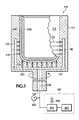
- FIG. 1 is a cross-sectional, somewhat schematic view, of an apparatus capable of manufacturing a crucible in accordance with one embodiment of the present invention.
- FIG. 1 is a cross section of a mold 112 with two layers of silica grain formed in the mold ready for fusing. As will be explained, the fusion process includes five stages.
- an apparatus 110 for manufacturing silica glass crucible may be provided as described in U.S. Patent App. No. 11/223,158 , which is incorporated herein by reference in its entirety.
- the apparatus 110 may include a rotating mold 112 having an inner mold surface 114 that defines a mold cavity.
- a plurality of air channels communicate with inner mold surface 114.
- Each air channel 118 and 120 comprises a cylindrical bore that creates a circular opening, like opening 122 in inner mold surface 114.
- Each air channel, like channel 120 includes a porous graphite plug 126 that prevents silica grain from being drawn from the mold cavity into the air channels.
- the air channels communicate with manifolds, like manifolds 128, 130, 132, which in turn communicate with a bore 134.
- An evacuation system 501 is connected to bore 134.
- the evacuation system 501 is configured to draw air from the mold cavity via the air channels and ultimately through bore 134 and out of apparatus 110.
- the evacuation system is configured for programmable evacuation power, at least for controlling starting and stopping times.
- an evacuation pump 502 has a set of control valves 504, which includes at least a leak valve 503, which vents to the room atmosphere.
- a pressure gauge 505 is connected to the evacuation bore 134. The pressure reading is used as an indication of pressure at the fusion front.
- mold 112 contains a natural quartz grain layer 228 and a pure silica grain layer 230 (which are shown partially broken away to expose the inner mold surface 114).
- the natural quartz grain layer 228 and the pure silica grain layer 230 are collectively referred to as the entire silica grain layer.
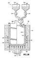
- FIGS. 2A and 2B are cross-sectional, somewhat schematic views, illustrating a method of forming silica grain layers using a feed system in accordance with one embodiment of the present invention.
- the feed system 210 may, for example, include a natural quartz grain hopper 212 containing natural quartz grain 214, a pure silica grain hopper 216 containing pure silica grain 218, valves 220 and 222 and a feed tube 224.
- a spatula 226 may also be provided that is vertically movable into and out of mold 112. The spatula 226 may further be horizontally movable within the mold 112 to shape the silica grain as the mold 112 rotates about the vertical axis 136.
- the natural quartz grain 214 contains impurities such as Al, Ca, Li and K.
- the natural quartz grain 214 may have, in part, an Al content of about 6 ppm; Ca content of about 1.3 ppm; Li content of about 0.7 ppm; K content about 0.1 ppm; and Na content of about 0.05 ppm.
- the pure silica grain 218 is synthesized from silicon tetra chloride purified through a distillation processes.
- the pure silica grain may have a total metallic content of less than 1 ppm, with an Al content of less than 0.2 ppm.
- silica grain The flow of natural quartz grain 214 and pure silica grain 218 (collectively referred to as "silica grain") from grain hoppers 212 and 216 may be controlled by regulating valves 220 and 222, respectively.
- the feed tube 224 introduces the flow of silica grain into mold 112 from either one of the hoppers, depending upon how valves 220 and 222 are set.
- the mold 112 is rotated about the vertical axis 136 at a rate of about 70 rpm to about 150 rpm, the feed tube 224 is positioned adjacent to the inner mold surface 114, and valve 220 is opened to begin depositing natural quartz grain 214 to form a natural quartz grain layer 228 about the perimeter of the mold cavity.
- the thickness of the natural quartz grain layer 228 (measured along a radial axis of the mold 112) is defined by the position of spatula 226. In one embodiment, the thickness of the natural quartz grain layer 228 may have a range of about 15 mm to about 30 mm.
- valve 220 is closed and valve 222 is opened while the mold 112 is rotated about the vertical axis 136.
- a pure silica grain layer 230 coats the inner surface of the natural quartz grain layer 228.
- the thickness of the pure silica grain layer 230 may have a range of about 1 mm to about 5 mm.
- the thickness of the entire silica grain layer, which is the combined thickness of the natural and pure silica grain layers 228 and 230, may be about 25 mm to 30 mm.
- the feed system 210 and the spatula 226 are moved out of the rotating mold 112 so that the entire silica grain layer may be fused to form a crucible.
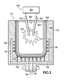
- FIG. 3 is a cross-sectional, somewhat schematic view, illustrating a method of fusing an entire silica grain layer using a grain fusing system 310 in accordance with one embodiment of the present invention.
- the grain fusing system has a programmable power supply 316 and electrodes 312 and 314 connected to the power supply.
- the programmable range of the power supply 316 is from 50 kVA to 1200 kVA.
- a grain fusing system 310 is moved into the cavity of the rotating mold 112 to fuse the entire silica grain layer.
- Hot arc plasma 318 fuses the entire silica grain layer thereby forming a crucible 320.
- Crucible 320 has layers 322, 324 that do not necessarily correspond to grain layers 228, 230 (in FIG. 2B ). Rather layers 322, 324 are formed as a result of different steps in the following described process.
- layer 322 may include part of pure silica layer 230, all of layer 230, or all of layer 230 and part of natural quartz grain layer 230.
- the evacuation system 501 is operated as programmed and gas is drawn from the interior of the rotating mold 112, through the entire silica grain layer into the air channels, like air channels 118 and 120. Generally, fusion of the entire silica grain layer starts at the innermost surface. The fusion front then moves outwards until it stops, leaving a thin unfused grain layer 326 between crucible 320 and inner mold surface 114.
- the fusion process can be divided into five stages defined by variations among fusion power, fusion front location and vacuum at the fusion front.
- FIGS. 4A-4D illustrate successive steps in the process with the unhatched portions representing unfused grain and the hatched portions representing different layers of fused grain.
- a first general description of the five stages is provided with reference to Table 1 and FIGS. 4A-4D followed by a more detailed description of the process in accordance with the Table 1 parameters.
- the first stage is starting of skin formation.
- Skin 402 is formed with bore 134substantially at atmospheric pressure.
- the evacuation system 501 is stopped by opening the leak valve 503 to the air while running the pump 502.
- evacuation system 501 is not activated at this skinning stage because evacuation may be harmful to uniformity of the skin.
- the mold is designed to locate air channels, like 118 and 120, where high levels of bubble-free characteristics and less-bubble-growth characteristics are required. These are typically at the corner radius and bottom of the crucible, because when the formed crucible is used in the CZ process, duration of the contact with silicon melt is significant there. If the evacuation system is activated before a skin is formed, hot plasma gas is directed to the air channels.
- stage 100 100 skin complete pure silica / slow 100 negligible skin complete under vacuum 3rd.
- stage 600 100 bubble free layer natural quartz / fast 100 medium clear layer formed mainly from natural quartz grain 4th.
- stage 600 30 opaque layer natural quartz / fast 30 medium opaque layer formed 5th.
- stage 850 30 skin removal natural quartz / almost stop 30 high pure silica skin sublimated, small portion of natural layer can be sublimated also
- One sophisticated method to manipulate the location of skinning is to provide another set of air channels (not shown in these embodiments) other than those air channels prepared for bubble free areas, and to accelerate skinning by evacuating through these channels. But stopping air flow through the air channels during skin formation while controlling the power and position of the electric arc is practically sufficient and economical to produce a uniform and thin skin.
- the second stage is completion of skin and starting of evacuation. Most of the surface of the grain layer is covered by a skin 402, so that pressure at the fusion front can be lowered at this stage by activating the evacuation system 501. Because the skin is not perfect especially at the upper portions of the mold, pressure at the fusion front is strongly related to the "leakage" through the unfused grain between the skin 402 and the inner mold surface 114.
- fusion power is controlled at the required minimum to form a skin, otherwise skin 402 will become too thick to be sublimated off later.
- the skin 402 after activating evacuation system 501 can be free of bubbles but would show bubble-growth during CZ process. This is probably because silica glass fused at low power is not well degassed and therefore shows bubble-growth at high temperatures like the CZ process.
- the evacuation system is activated by closing the leak valve 503.
- fusion power is increased as soon as the evacuation system is activated. In one embodiment of this invention, fusion power was increased 10 seconds after evacuation system was activated.
- the third stage fuses a bubble free layer under the skin 402 by increasing fusion power.
- the evacuation system 501 has been activated at the end of stage two.
- the relatively long distance from the upper surfaces of the entire silica grain layer to the first openings increases the resistance to pump flow.
- This increases the pressure drop between the atmosphere above the upper surfaces of the entire silica grain layer and the manifolds 128, 130 and 132.
- the pressure at the fusion front is reduced and gas is rapidly drawn away from the fusion front and into the manifolds 128, 130 and 132 by the pump 502.
- high power fusion is required to reduce bubble growth when the crucible will be used in the CZ process.
- High power fusion is presumed to help degassing the fused silica glass.
- electric power to the electrode is increased to 600 kVA at the third stage.
- a bubble-free layer can be pure silica glass or a combination of pure silica glass formed from grain layer 230 and natural quartz glass formed from grain layer 228. This bubble-free layer constitutes inner crucible layer 322.
- the fourth stage fuses opaque outer crucible layer 324 outside of the inner crucible layer 322.
- evacuation power By reducing evacuation power, bubbles can be introduced at the fusion front.
- controlled vacuum and relatively high power are required at this stage.
- a set of the controlling valves 504 is operated to keep 680 Torr. at the pressure gauge 505 while applying 600 kVA to the electrodes.
- the fifth stage of fusion is removal of the above mentioned skin 402.
- the skin 402 was fused at low fusion power and mainly at atmospheric pressure, the skin 402 is not bubble-free and those bubbles would grow during a CZ process. This skin 402 therefore has to be removed.
- the best method to remove the skin is sublimation of the silica glass that forms the skin.
- electric power was boosted by 42%, from 600 kVA to 850 kVA.
- the power level and boosted step can be altered depending on the apparatus configurations, such as shielding, efficiency of power supply and ventilation in the crucible interior.
- the fusion front almost stops at a saturated point leaving some unfused grain 326 between mold 112 and crucible 320 at the end of stage four.
- This fifth stage can be combined to or overlapped with the third and/or fourth stage, because some amount of sublimation normally occurred at these stages. However, an additional stage removes the skin thoroughly.
- the fifth stage is preferably designed for sublimation only, minimizing progress of the fusion front. Another reason to sublimate at the final stage is to prevent deposits of sublimated material on the electrodes, which then drop back into the crucible resulting in "fume-deposit" defects on the crucible.
- the fifth stage, or sublimation stage is required to minimize aluminum build up left after sublimation of the skin, which naturally occurs during the earlier stages. Removing the skin requires more intense sublimation than would normally occur.
- pure silica glass corresponding to 0.8 mm to 1.2 mm thickness of pure silica grain layer is used to make the skin that is then later sublimated. This layer is fused from grain that is in pure silica grain layer 230 in FIG. 2B .
- the design of the final crucible structures, including the bubble free layer, purity profile in the crucible layers, grain forming, fusion power program and evacuation programs may be customized.
- the innermost layer of pure silica grain can be thicker than that required for skin formation.
- the crucible may a have bubble free and bubble-growth free pure silica layer on the natural quartz glass layer.
- bubble structure of the final crucibles can be finely controlled to desired qualities and depths.
- the inner half of the bubble free layer was made from pure silica grain and the outer half of the bubble free layer and the opaque outer layer were made from natural quartz glass ( FIGS 5A-5D ).
- the effects of a CZ process on the crucible 320 can be estimated by performing a vacuum bake test simulating a CZ process.
- a vacuum bake test can include heating the crucible piece at about 1650 °C for three hours at a pressure of 0.1 Pa. argon atmospheres.
- the crucibles according to the present invention do not have localized bubble containing areas or areas that show bubble growth in response to this vacuum bake test, especially on the bottom and around the corner radius. Accordingly, disturbances in the single-crystalline structure of a silicon ingot pulled during a CZ process attributable to particle generation as a result of bubble dissolution from the inner crucible layer 322, are prevented.
- FIGS. 4A-4D are cross-sectional views illustrating a method of fusing a crucible at various stages of a crucible-fusion process, according to one embodiment of the present invention.
- Table 1 is a summary of the five stages according to the above mentioned embodiment of the present invention.
- electric power to the arc is shown in units of kVA.
- the evacuation power is shown in arbitrary units.
- the value 100 corresponds to the reading of gauge 505 with vacuum pump operation at 800 m 3 /hr. Main events at each the stages are described in the table. The grain to be fused at each stage is described along with the qualitative speed of fusion front progression.
- the vacuum level or pressure at the fusion front is shown using arbitrary units. Because the pressure is not uniform for the whole fusion front, the numbers are understood as relative numbers.
- the value 5 is almost atmospheric pressure at the gauge 505 and the value 100 is about 150 Torr. at the gauge 505. Amount of sublimation and comments are also given in the table.
- a portion of the pure silica grain layer 230 at the innermost surface is fused to form a skin layer 402.
- power applied to the electrodes 312 and 314 may be about 100 kVA or less. In one embodiment, the power applied to the electrodes 312 and 314 may have a range from about 40 kVA to about 80 kVA.
- the evacuation system 501 may be stopped, such that a pressure measured at gauge 505 is about 760 Torr.
- the skin layer 402 may contain bubbles. Because the skin layer 402 is formed by fusing at relatively low electric power, the skin layer may also show bubble growth in a CZ process.
- the evacuation system 501 is activated.
- pump 502 was kept running during stage 1 and stage 2 with the leak valve 503 open to the air so as not to evacuate gas through the bore 134.
- the pressure measured at the gauge 505 may be dropped to 150 Torr. after the evacuation system is activated.
- stage 3 power applied to the electrodes 312 and 314 may be about 600 kVA.
- the evacuation system 501 is kept running to ensure that the natural quartz glass layer 404a contains substantially no bubbles.
- the duration of stage 3 may correspond to a time sufficient to ensure that the inner layer 322, which is the same as 404a in the case of FIGS. 4A-D , has a thickness of about 2.0 mm to about 6.0 mm.
- the pump 502 may be operated during stage 3 to evacuate gas at the flow rates in a manner described in U.S. Patent App. No. 11/223,158 , which is incorporated herein by reference in its entirety, to form the inner layer 322.
- Some of the skin layer 402 may be sublimated during stage 3, but the amount is relatively small.
- the fourth stage of the crucible-fusion process a remaining portion of the entire silica grain layer, which is natural quartz grain layer in this case, is fused to form opaque outer crucible layer 324.
- the opaque natural quartz glass layer composes the outer layer 324.
- the evacuation power is reduced to introduce a sufficient amount of bubbles while assuring fusion power is large enough to reduce bubble growth during the CZ process, in a manner described in U.S. Patent App. No. 11/223,158 .
- the fusion front is almost stopped at the equilibrium position between heating by electric arc from inside and cooling resulting from contact with cold wall of the mold. In one embodiment of this invention, the fusion front is nearly stopped when power is removed leaving 2 mm to 3 mm unfused grain 326 between fused crucible 320 and an inner mold surface 114.
- the fifth stage of the crucible-fusion process is to eliminate the skin 402 by sublimation.
- the fusion power is applied not for fusing the entire silica grain layer to the target dimensions, but mainly for sublimation of the skin 402.
- the power applied to the electrodes 312 and 314 was 850 kVA.
- about 0.1 mm to about 2.0 mm of the pure silica glass may be sublimated to ensure that the skin layer 402 is sufficiently removed.
- about 0.6 mm of the pure fused silica layer 402 is sublimated to ensure that the skin layer 402 is sufficiently removed.
- the inner crucible layer 322 has a thickness of about 2.0 mm to about 6.0 mm after removal of the skin 402.
- the pure silica grain is mainly used for skin and is sublimated later, leaving the innermost surface of the crucible inner layer 322 similar to a natural quartz glass.
- FIG. 6 shows the impurity profile on the crucible inner layer 322 at the one embodiment of this invention. Three consecutive surface layers with about 30 micrometers in thickness, were etched off and analyzed. The innermost layer was 14 ppm Al, 0.2 ppm Ca, 0.6 ppm Li and less than 0.14 ppm K.
- FIGS. 5A-5D Another embodiment of this invention is illustrated in FIGS. 5A-5D with Table 2.
- the formed grain layers as shown in FIG. 5A are different from the previous case shown in FIG. 4A .
- Pure silica grain layer 230 is thicker than that required for the skin.
- the bubble free layer fused at the stage 3 is fused from pure silica grain 230 and from natural quartz grain layer 228 as shown in FIG. 5B .
- Normally a crucible should have a thicker bubble free layer than the layer that is dissolved during CZ process.
- the bubble free layer is designed to have pure silica layer 404b and natural quartz glass layer 404a.
- stage 100 5 skin start evenly pure silica / slow 5 negligible skin at atmospheric pressure Skin is even in thickness 2nd.
- stage 100 100 skin complet e pure silica / slow 100 negligible skin complete under vacuum 3rd.
- stage 600 100 bubble free layer natural quartz + pure silica / fast 100 medium clear layer formed, purity wise double layer [pure / natural] 4th.
- stage 600 30 Opaque layer natural quartz / fast 30 medium opaque layer formed 5th.
- stage 850 30 Skin removal natural quartz / almost stop 30 high pure silica skin sublimated leaving pure silica surface
- Opaque outer crucible layer 324 is fused as shown in FIG. 5C in a similar way as shown in FIG. 4C .
- FIG. 5D is illustration of the completion of the fusion process.
- the crucible processed as shown in the Table 2 has a pure silica bubble-free layer as an inner portion of the inner layer 322.
- pure silica grain was formed with less than 0.2 ppm for all of Al, Ca, Li, Na and K.
- the innermost surface layer with about 30 micrometers in thickness had 2 ppm Al, 0.2 ppm Ca, 0.5 ppm Li and less than 0.1 ppm K.
- the impurity profile observed by three layer analysis is shown in the FIG. 7 . The observed increase of impurities is supposed to be attributed to diffusion from natural quartz glass layer 404a.
- stage 600 100 bubble free layer natural quartz + pure silica / fast 100 medium clear layer formed, purity wise double layer [pure / natural] 4th.
- stage 600 30 opaque layer natural quartz / fast 30 medium opaque layer formed 5th.
- stage 850 30 skin removal natural quartz / almost stop 30 high pure silica skin sublimated, but not completely, leaving partial skin which was fused at low power
- Table 4 shows a traditional known method of making a crucible, as described in U.S. Patent App. No. 11/223,158 for example.
- Table 4 (Crucible D - Traditional method ⁇ comparative example>) electric power evacuation power event fused grain / fusion front pressure at fusion front sublimation comment 1st. stage + 2nd.
- stage 100 100 skin uneven pure silica / skin complete fast 10 --- 20 negligible skin at atmospheric pressure Skin is uneven and localized 3rd.
- stage -1 500 100 bubble free layer pure silica / fast 70 medium low clear layer formed, while skin is not completed 3rd.
- stage -2 600 100 bubble free layer natural quartz + pure silica / fast 100 medium clear layer formed, purity wise double layer [pure / natural] 4th.
- stage -2 600 10 opaque layer natural quartz / almost stop 30 medium high sublimation not enough to eliminate skin, localized thick skin can not be
- FIGS. 6, 7 and 8 comprise graphs of the impurities within the innermost wall of each of crucibles A, B and D, respectively.
- the L1 data point in each graph was established by etching the innermost crucible layer to a depth of 30 micrometers and analyzing the etched solution.
- the L2 data point was established by further etching another 30 micrometers and analyzing the etched solution with the L3 data point resulting from further etching and analyzing another 30 micrometers.
- FIG. 9 is a core sample including an innermost layer 1001, which is used to create the impurity profile shown; a pure silica layer 1002, which includes layer 1001; a bubble free and slow-bubble growth layer 1003, which includes layers 1001, 1002; and an opaque layer 1004, which includes bubbles that extend between layer 1003 and the radially outer surface 1005 of the crucible.
- the graphs below the sample show the Aluminum across the wall of the crucible for two different processes, one for Crucible D, as described in Table 4 and one for Crucible B, as described in Table 2.
- Crucible D was used in a CZ process; it presented difficulties in starting pulling. Several retrials were required to start pulling.
- a natural quartz grain was formed in the rotating mold as natural grain layer.
- a synthetic silica grain with 3.5 mm in thickness was formed as a pure silica grain layer on the natural quartz grain layer.
- the synthetic silica grain contained less than 0.2 ppm of each of Al, Ca, Li, Na and K.
- the natural quartz grain had, 6 ppm Al, 1.3 ppm Ca, 0.7 ppm Li, 0.05 ppm Na and 0.1 ppm K.
- the rotating mold had a cavity with a diameter of 463 mm.
- a programmable DC power supply of 1000 kVA was connected to the graphite electrodes.
- the evacuation system had evacuation capacity of 800 m 3 /hr and a set of valves and piping to control evacuation power.
- the total of the first and the second stage took 2 minutes.
- the evacuation system was inactivated by opening the leak valve and activated (by closing the valve) at 1 minutes and 50 seconds.
- the electric power at stage 1 and stage 2 was 60 kVA to 100 kVA.
- the vacuum sensor located by the evacuation bore 134 was used to monitor pressure at the fusion front. The reading does not represent the pressure at the fusion front, but indicates relative values.
- the pressure reading at stage 3 was 150 Torr.
- the electric power was raised from 100 kVA to 600 kVA for stage 3 and stage 4.
- the evacuation system was tuned to 680 Torr. at the sensor position.
- One crucible was cut to coupons for vacuum bake test. After performing a vacuum bake test in which the crucible was baked at approximately 1650 °C for approximately three hours at a pressure of approximately 0.1 Pa. argon, it was determined that the crucible had an inner crucible layer 3.5 mm thick, which was substantially free of bubbles and showed no significant bubble growth.
- the crucible was used for CZ process without any problems associated with crystalline structures.
- a crucible was prepared according to the same procedure outlined for the Test Example 1, except that a 1.5 mm thick synthetic silica grain layer was formed on the natural quartz grain layer.
- the crucible performed equally well concerning structure loss.
- the silicon melt should have more impurities than the case of example 1, but was not critical with respect to structure loss.
- a crucible was prepared according to the same procedure outlined for the Test Example 1, except fusion stages were taken as shown in Table 3. The biggest difference is that the evacuation system has been activated from the beginning of stage 1.
- a vacuum bake test results showed a layer of bubbles around the corner radius, indicating that the skin was not completely removed.
- the crucible was used at CZ process, but three repeated trials were required before successful start of the pulling single crystal.
- a crucible was prepared according to the same procedure outlined for the Test Example 1, except that no synthetic grain silica layer was formed on the natural quartz grain layer.
- the fusion stages are as shown in the Table 4. There is no fifth stage for intentional sublimation. Fusion was stopped when required dimensions, diameters and wall thicknesses, were met.
- the impurity profiles are shown in FIG. 8 . Even there was no sublimation stage at high powers, such as 850 kVA, a huge impurity pile up was observed.
- Aluminum content in the first layer L1 was 110 ppm, which is order 7.8 times larger than Example 2 and 55 times more than Example 1.
Landscapes
- Chemical & Material Sciences (AREA)
- Engineering & Computer Science (AREA)
- Materials Engineering (AREA)
- Organic Chemistry (AREA)
- Manufacturing & Machinery (AREA)
- Crystallography & Structural Chemistry (AREA)
- Metallurgy (AREA)
- Crystals, And After-Treatments Of Crystals (AREA)
- Glass Melting And Manufacturing (AREA)
Abstract
Description
- Embodiments of the present invention generally relate to methods of making silica crucibles. More particularly, embodiments of the present invention relate to methods of making silica crucibles with highly pure and bubble free inner crucible layers.
- There are several methods for making single crystal silicon materials. One such process - the "Czochralski" (CZ) process - has been widely adopted for producing single crystal silicon materials for semiconductor applications including solar cell applications. In the CZ process, molten silicon is contained within a vessel and a tip of a single-crystalline seed crystal is dipped into the molten silicon. The seed crystal is then "pulled" while being rotated. As a result, a single crystal silicon ingot is grown from the molten silicon.
- A crucible is one vessel commonly employed in this pulling operation for making silicon ingots. Crucibles are typically configured in a bowl shape to contain the molten silicon during the pulling operation. Crucibles are made of silica glass, or quartz glass, to introduce a desired amount of oxygen into the molten silicon while keeping if from contamination with metallic impurities.
- During the CZ process, the inner surface of a silica glass crucible typically dissolves into the molten silicon. Any bubbles present in the inner crucible layer may open to the melt by dissolution and are a potential source of particles that may disturb the single-crystalline structure of the silicon ingot. Therefore, crucibles are typically manufactured to have a bubble-free inner crucible layer. The outer crucible layers are typically manufactured to contain numerous tiny bubbles to facilitate scattering of radiation from heater elements.
- To minimize the possibility of contamination of the silicon ingot during the CZ process, the inner crucible layer should be as pure as possible.
- Silica glass made from natural quartz grain often contains an Al content of 5-20 ppm. The Al element in the silica glass is often associated with positively charged metallic impurities such as Li, Ca and Na. Therefore, reduction of Al content is desirable to minimize concentration of other metallic elements (here and in the following, the term "ppm" always refers to parts per million of weight).
- One known method of manufacturing silica glass crucibles or quartz glass crucibles, is to form silica grain, which can be synthetic silica grain or natural quartz grain, in a crucible shape inside of a rotating mold, then fuse it into a silica glass crucible. The crucible is taken out of the mold and mechanically finished and cleaned to a final product.
- During fusion, silica sublimates from the inner surface of the inner crucible layer. As silica sublimates faster than alumina, when natural quartz grain is used as the starting material, aluminum is left on the inner surface of the inner crucible layer. As mentioned above, aluminum is associated with other metallic impurities.
- One method disclosed in Japanese Patent
JP 63-166791 - Another known method of manufacturing quartz glass crucibles, disclosed in
U.S. Patent No. 6,510,707 , is understood to make the inner crucible layer bubble-free with little bubble growth and reduce the Al content at the inner surface of the inner crucible layer. A crucible is fused by employing a relatively large amount of electrical power to reduce bubble and bubble growth leaving an aluminum-rich layer on the surface of the inner crucible layer. The aluminum-rich layer is then removed by abrasive processes or etching processes. While this method can produce an inner crucible layer that may be relatively bubble-free with little bubble growth during the CZ process, abrading or etching the aluminum rich layer is time consuming and not economical. - Consequently it would be desirable to prepare a silica crucible having an inner crucible layer with minimal impurity concentration and reduced bubble and bubble-growth at reasonable cost.
- The present invention attains the above-described objects relates to a method of making a silica crucible in a mold cavity of the type in which air can be drawn through silica grain in the cavity comprising:
- forming a first silica grain layer in the mold cavity;
- forming a second, pure silica grain layer on the first silica grain layer;
- fusing at least a portion of the second silica grain layer while drawing no air or a first volume of air through the silica grain;
- fusing any remaining portion of the second silica grain layer and at least a portion of the first silica grain layer while drawing a second volume of air which is higher than the first volume of air through the silica; and
- sublimating at least a portion of the fused second silica grain layer.
- In a preferred embodiment, the second silica grain layer contains less than 20 ppm aluminum, preferably less than 4 ppm aluminum.
- In a further preferred embodiment, the thickness of the second silica grain layer is less than 3 mm, preferably less than 1.5 mm, and the thickness of the sublimated portion is more than 0.5 mm, preferably more than 0.8 mm.
- In a further preferred embodiment, fusing at least a portion of the second silica grain layer comprises doing so at a relatively low fusion power and wherein fusing any remaining second silica layer and at least a portion of the first silica grain layer further comprises doing so at a second fusion power higher than the relatively low fusion power.
- Preferably, the relatively low fusion power is less than 300 kVA, preferably less than 200 kVA.
- In this context, it was found suitable sublimating at least a portion of the fused second silica grain layer comprises doing so at a third fusion power that is higher than the second fusion power, preferably it is more than 700 kVA.
- More preferably, the relatively low fusion power is less than 300 kVA and wherein the method further comprises:
- raising the relatively low fusion power to more than 500 kVA; and
- drawing the higher volume of air through the silica no less than 20 seconds before the fusion power is raised to more than 500 kVA.
- In a further preferred embodiment the method further comprises fusing at least a portion of the second silica grain layer while drawing no air or a first volume of air through the silica grain for more than 30 seconds, preferably for more than 60 seconds.
- In a further preferred embodiment sublimating at least a portion of the fused second silica grain layer comprises sublimating at least a portion of the fused second silica grain layer for between 20 seconds and 240 seconds, preferably less than 120 seconds at a fusion power greater than 700 kVA.
- In a further preferred embodiment after sublimating at least a portion of the fused second silica grain layer, the remaining fused silica grain layer having an almost bubble free thickness between 2 mm and 6 mm.
- In a further preferred embodiment sublimating at least a portion of the fused second silica grain layer comprises sublimating the entire fused second silica grain layer.
- In a further preferred embodiment:
- the fusing of at least a portion of the second silica grain layer occurs at a first temperature; and
- the fusing at least a portion of the first silica grain layer occurs at a second temperature higher than the first temperature.
- In a further preferred embodiment fusing at least a portion of the second silica grain layer comprises
- fusing a first portion of the second silica grain layer while drawing no air or a first volume of air through the silica grain layer at a relatively low fusion power;
- fusing a second portion of the second silica grain layer while drawing a second, higher volume of air through the silica grain layer at a relatively high fusion power;
- and then fusing at least a portion of the first silica grain layer while drawing the higher volume of air through the silica grain layer; and sublimating the entire fused first portion of the second silica grain layer.
- In this context it is preferred that the thickness of the fused portions formed while drawing a higher volume of air through the silica grain is 2.0 mm to 6.0 mm.
- In a further preferred embodiment a dense inner silica layer is formed by the fusing of at least a portion of the second silica grain layer; and after forming the inner silica layer, air is drawn through a portion of unfused silica grains while fusing at least a portion of the remaining unfused silica grains.
-
-
FIG. 1 is a cross-sectional, somewhat schematic, view of an apparatus capable of producing a crucible in accordance with one embodiment of the present invention. -
FIGS. 2A and2B are cross-sectional, somewhat schematic, views illustrating a method of forming silica grain layers using a feed system in accordance with one embodiment of the present invention. -
FIG. 3 is a cross-sectional, somewhat schematic, view illustrating a method of fusing silica grain layers using a grain fusing system in accordance with one embodiment of the present invention. -
FIGS. 4A-4D are cross-sectional views illustrating a method of fusing a crucible at various stages of a crucible-manufacturing process, according to one embodiment of the present invention. -
FIGS. 5A-5D are cross-sectional views illustrating a method of fusing a crucible at various stages of a crucible-manufacturing process, according to another embodiment of the present invention. -
FIG. 6 shows the impurity profile at the surface of the inner crucible layer, according to one embodiment of the present invention. -
FIG. 7 shows the impurity profile at the surface of the inner crucible layer, according to another embodiment of the present invention. -
FIG. 8 shows the impurity profile at the surface of the inner crucible layer, according to a traditional method of manufacturing a crucible. -
FIG. 9 illustrates a core sample from a crucible and a corresponding Aluminum profile for one process according to an embodiment of the invention and another comparative process. -
FIG. 1 is a cross-sectional, somewhat schematic view, of an apparatus capable of manufacturing a crucible in accordance with one embodiment of the present invention. -
FIG. 1 is a cross section of amold 112 with two layers of silica grain formed in the mold ready for fusing. As will be explained, the fusion process includes five stages. - Referring to
FIG. 1 , anapparatus 110 for manufacturing silica glass crucible may be provided as described inU.S. Patent App. No. 11/223,158 , which is incorporated herein by reference in its entirety. For example, theapparatus 110 may include arotating mold 112 having aninner mold surface 114 that defines a mold cavity. - A plurality of air channels, like
channels inner mold surface 114. Eachair channel inner mold surface 114. Each air channel, likechannel 120, includes aporous graphite plug 126 that prevents silica grain from being drawn from the mold cavity into the air channels. The air channels communicate with manifolds, likemanifolds bore 134. Anevacuation system 501 is connected to bore 134. - The
evacuation system 501 is configured to draw air from the mold cavity via the air channels and ultimately throughbore 134 and out ofapparatus 110. The evacuation system is configured for programmable evacuation power, at least for controlling starting and stopping times. In one embodiment, anevacuation pump 502 has a set ofcontrol valves 504, which includes at least aleak valve 503, which vents to the room atmosphere. Apressure gauge 505 is connected to the evacuation bore 134. The pressure reading is used as an indication of pressure at the fusion front. - In one embodiment,
mold 112 contains a naturalquartz grain layer 228 and a pure silica grain layer 230 (which are shown partially broken away to expose the inner mold surface 114). The naturalquartz grain layer 228 and the puresilica grain layer 230 are collectively referred to as the entire silica grain layer. - The procedures to form two layers of silica grain are explained using
FIGS. 2A and2B .FIGS. 2A and2B are cross-sectional, somewhat schematic views, illustrating a method of forming silica grain layers using a feed system in accordance with one embodiment of the present invention. - Referring generally to
FIGS. 2A and2B , thefeed system 210 may, for example, include a naturalquartz grain hopper 212 containingnatural quartz grain 214, a puresilica grain hopper 216 containingpure silica grain 218,valves feed tube 224. Aspatula 226 may also be provided that is vertically movable into and out ofmold 112. Thespatula 226 may further be horizontally movable within themold 112 to shape the silica grain as themold 112 rotates about thevertical axis 136. - In one embodiment, the
natural quartz grain 214 contains impurities such as Al, Ca, Li and K. Thenatural quartz grain 214 may have, in part, an Al content of about 6 ppm; Ca content of about 1.3 ppm; Li content of about 0.7 ppm; K content about 0.1 ppm; and Na content of about 0.05 ppm. - In one embodiment, the
pure silica grain 218 is synthesized from silicon tetra chloride purified through a distillation processes. In one embodiment, the pure silica grain may have a total metallic content of less than 1 ppm, with an Al content of less than 0.2 ppm. - The flow of
natural quartz grain 214 and pure silica grain 218 (collectively referred to as "silica grain") fromgrain hoppers valves feed tube 224 introduces the flow of silica grain intomold 112 from either one of the hoppers, depending upon howvalves - Referring to
FIG. 2A , themold 112 is rotated about thevertical axis 136 at a rate of about 70 rpm to about 150 rpm, thefeed tube 224 is positioned adjacent to theinner mold surface 114, andvalve 220 is opened to begin depositingnatural quartz grain 214 to form a naturalquartz grain layer 228 about the perimeter of the mold cavity. The thickness of the natural quartz grain layer 228 (measured along a radial axis of the mold 112) is defined by the position ofspatula 226. In one embodiment, the thickness of the naturalquartz grain layer 228 may have a range of about 15 mm to about 30 mm. - Referring to
FIG. 2B , after the naturalquartz grain layer 228 is formed,valve 220 is closed andvalve 222 is opened while themold 112 is rotated about thevertical axis 136. Aspure silica grain 218 feeds from the puresilica grain hopper 216 out of feed tube 224 a puresilica grain layer 230 coats the inner surface of the naturalquartz grain layer 228. In one embodiment, the thickness of the puresilica grain layer 230 may have a range of about 1 mm to about 5 mm. In one embodiment, the thickness of the entire silica grain layer, which is the combined thickness of the natural and pure silica grain layers 228 and 230, may be about 25 mm to 30 mm. - After forming the pure
silica grain layer 230, thefeed system 210 and thespatula 226 are moved out of therotating mold 112 so that the entire silica grain layer may be fused to form a crucible. -
FIG. 3 is a cross-sectional, somewhat schematic view, illustrating a method of fusing an entire silica grain layer using agrain fusing system 310 in accordance with one embodiment of the present invention. The grain fusing system has aprogrammable power supply 316 andelectrodes power supply 316 is from 50 kVA to 1200 kVA. - Referring to
FIG. 3 , after thefeed system 210 is withdrawn from the rotatingmold 112, agrain fusing system 310 is moved into the cavity of therotating mold 112 to fuse the entire silica grain layer.Hot arc plasma 318 fuses the entire silica grain layer thereby forming acrucible 320.Crucible 320 haslayers grain layers 228, 230 (inFIG. 2B ). Rather layers 322, 324 are formed as a result of different steps in the following described process. As will be seen,layer 322 may include part ofpure silica layer 230, all oflayer 230, or all oflayer 230 and part of naturalquartz grain layer 230. - The
evacuation system 501 is operated as programmed and gas is drawn from the interior of therotating mold 112, through the entire silica grain layer into the air channels, likeair channels unfused grain layer 326 betweencrucible 320 andinner mold surface 114. - The fusion process can be divided into five stages defined by variations among fusion power, fusion front location and vacuum at the fusion front.
FIGS. 4A-4D illustrate successive steps in the process with the unhatched portions representing unfused grain and the hatched portions representing different layers of fused grain. A first general description of the five stages is provided with reference to Table 1 andFIGS. 4A-4D followed by a more detailed description of the process in accordance with the Table 1 parameters. - Referring to Table 1, the first stage is starting of skin formation.
Skin 402 is formed with bore 134substantially at atmospheric pressure. In one embodiment of this invention, theevacuation system 501 is stopped by opening theleak valve 503 to the air while running thepump 502. In this embodiment,evacuation system 501 is not activated at this skinning stage because evacuation may be harmful to uniformity of the skin. Normally the mold is designed to locate air channels, like 118 and 120, where high levels of bubble-free characteristics and less-bubble-growth characteristics are required. These are typically at the corner radius and bottom of the crucible, because when the formed crucible is used in the CZ process, duration of the contact with silicon melt is significant there. If the evacuation system is activated before a skin is formed, hot plasma gas is directed to the air channels. As the result, thick skin is formed at the air channel positions, and thinner skin is formed elsewhere. This produces a skin of uneven thickness, which is difficult to remove by sublimation or otherwise. In addition, a thin uniform skin helps to lower the pressure at the fusion front at the air channel location.Table 1 (Crucible A) electric power evacuation Power event fused grain / fusion front pressure at fusion front sublimation comment 1st. stage 100 5 skin start evenly pure silica / slow 5 negligible skin at atmospheric pressure Skin is even in thickness 2nd. stage 100 100 skin complete pure silica / slow 100 negligible skin complete under vacuum 3rd. stage 600 100 bubble free layer natural quartz / fast 100 medium clear layer formed mainly from natural quartz grain 4th. stage 600 30 opaque layer natural quartz / fast 30 medium opaque layer formed 5th. stage 850 30 skin removal natural quartz / almost stop 30 high pure silica skin sublimated, small portion of natural layer can be sublimated also - One sophisticated method to manipulate the location of skinning is to provide another set of air channels (not shown in these embodiments) other than those air channels prepared for bubble free areas, and to accelerate skinning by evacuating through these channels. But stopping air flow through the air channels during skin formation while controlling the power and position of the electric arc is practically sufficient and economical to produce a uniform and thin skin.
- The second stage is completion of skin and starting of evacuation. Most of the surface of the grain layer is covered by a
skin 402, so that pressure at the fusion front can be lowered at this stage by activating theevacuation system 501. Because the skin is not perfect especially at the upper portions of the mold, pressure at the fusion front is strongly related to the "leakage" through the unfused grain between theskin 402 and theinner mold surface 114. - During the first and the second stages, fusion power is controlled at the required minimum to form a skin, otherwise
skin 402 will become too thick to be sublimated off later. Theskin 402 after activatingevacuation system 501 can be free of bubbles but would show bubble-growth during CZ process. This is probably because silica glass fused at low power is not well degassed and therefore shows bubble-growth at high temperatures like the CZ process. In one embodiment, the evacuation system is activated by closing theleak valve 503. In this embodiment, fusion power is increased as soon as the evacuation system is activated. In one embodiment of this invention, fusion power was increased 10 seconds after evacuation system was activated. - The third stage fuses a bubble free layer under the
skin 402 by increasing fusion power. Theevacuation system 501 has been activated at the end of stage two. Now, the relatively long distance from the upper surfaces of the entire silica grain layer to the first openings increases the resistance to pump flow. This, in turn, increases the pressure drop between the atmosphere above the upper surfaces of the entire silica grain layer and themanifolds manifolds pump 502. In addition to good skin coverage, which assures a good vacuum level, high power fusion is required to reduce bubble growth when the crucible will be used in the CZ process. High power fusion is presumed to help degassing the fused silica glass. In one embodiment, electric power to the electrode is increased to 600 kVA at the third stage. - Depending how thick the pure silica grain is, a bubble-free layer can be pure silica glass or a combination of pure silica glass formed from
grain layer 230 and natural quartz glass formed fromgrain layer 228. This bubble-free layer constitutesinner crucible layer 322. - The fourth stage fuses opaque
outer crucible layer 324 outside of theinner crucible layer 322. By reducing evacuation power, bubbles can be introduced at the fusion front. To control bubble size and bubble amount, and also to reduce bubble growth, controlled vacuum and relatively high power are required at this stage. In one embodiment, a set of the controllingvalves 504 is operated to keep 680 Torr. at thepressure gauge 505 while applying 600 kVA to the electrodes. - The fifth stage of fusion is removal of the above mentioned
skin 402. As theskin 402 was fused at low fusion power and mainly at atmospheric pressure, theskin 402 is not bubble-free and those bubbles would grow during a CZ process. Thisskin 402 therefore has to be removed. The best method to remove the skin is sublimation of the silica glass that forms the skin. In one embodiment of the present invention, electric power was boosted by 42%, from 600 kVA to 850 kVA. The power level and boosted step can be altered depending on the apparatus configurations, such as shielding, efficiency of power supply and ventilation in the crucible interior. - The fusion front almost stops at a saturated point leaving some
unfused grain 326 betweenmold 112 andcrucible 320 at the end of stage four. - This fifth stage can be combined to or overlapped with the third and/or fourth stage, because some amount of sublimation normally occurred at these stages. However, an additional stage removes the skin thoroughly. The fifth stage is preferably designed for sublimation only, minimizing progress of the fusion front. Another reason to sublimate at the final stage is to prevent deposits of sublimated material on the electrodes, which then drop back into the crucible resulting in "fume-deposit" defects on the crucible. The fifth stage, or sublimation stage, is required to minimize aluminum build up left after sublimation of the skin, which naturally occurs during the earlier stages. Removing the skin requires more intense sublimation than would normally occur. In one embodiment, pure silica glass corresponding to 0.8 mm to 1.2 mm thickness of pure silica grain layer is used to make the skin that is then later sublimated. This layer is fused from grain that is in pure
silica grain layer 230 inFIG. 2B . The design of the final crucible structures, including the bubble free layer, purity profile in the crucible layers, grain forming, fusion power program and evacuation programs may be customized. - There is a conflict between better sealing and better purity at the innermost layer. Thicker skin helps to form a better clear layer underneath, but thinner skin leaves less impurity leftover after the skin is sublimated. In one embodiment, a layer of pure silica grain of about 0.8 mm to 1.2 mm was used to form the skin. After taking off the skin by sublimation, the impurity profile is improved over the prior art. When, instead of pure silica grain, natural quartz grain was used for the skin, the impurity profile was stronger after sublimation.
- The innermost layer of pure silica grain can be thicker than that required for skin formation. After sublimation, the crucible may a have bubble free and bubble-growth free pure silica layer on the natural quartz glass layer. Depending on the thickness of the pure silica grain and when evacuation power is reduced, bubble structure of the final crucibles can be finely controlled to desired qualities and depths.
- In one embodiment, the inner half of the bubble free layer was made from pure silica grain and the outer half of the bubble free layer and the opaque outer layer were made from natural quartz glass (
FIGS 5A-5D ). - The effects of a CZ process on the
crucible 320 can be estimated by performing a vacuum bake test simulating a CZ process. For example, a vacuum bake test can include heating the crucible piece at about 1650 °C for three hours at a pressure of 0.1 Pa. argon atmospheres. - The crucibles according to the present invention do not have localized bubble containing areas or areas that show bubble growth in response to this vacuum bake test, especially on the bottom and around the corner radius. Accordingly, disturbances in the single-crystalline structure of a silicon ingot pulled during a CZ process attributable to particle generation as a result of bubble dissolution from the
inner crucible layer 322, are prevented. - An exemplary method of forming the above-described inner and outer crucible layers 322 and 324 will now be described in more detail with respect to
FIGS. 4A-4D and Table 1. -
FIGS. 4A-4D are cross-sectional views illustrating a method of fusing a crucible at various stages of a crucible-fusion process, according to one embodiment of the present invention. Table 1 is a summary of the five stages according to the above mentioned embodiment of the present invention. - In Table 1, electric power to the arc is shown in units of kVA. The evacuation power is shown in arbitrary units. The
value 100 corresponds to the reading ofgauge 505 with vacuum pump operation at 800 m3/hr. Main events at each the stages are described in the table. The grain to be fused at each stage is described along with the qualitative speed of fusion front progression. The vacuum level or pressure at the fusion front is shown using arbitrary units. Because the pressure is not uniform for the whole fusion front, the numbers are understood as relative numbers. On the low end, the value 5 is almost atmospheric pressure at thegauge 505 and thevalue 100 is about 150 Torr. at thegauge 505. Amount of sublimation and comments are also given in the table. - Referring to
FIG. 4A and Table 1, in the first stage of the crucible-fusion process, a portion of the puresilica grain layer 230 at the innermost surface is fused to form askin layer 402. Duringstage 1, power applied to theelectrodes electrodes stage 1, theevacuation system 501 may be stopped, such that a pressure measured atgauge 505 is about 760 Torr. - This condition continues to stage two where skin covers almost 80% of the final crucible shape. Because the major portion of the
skin layer 402 is formed by fusing without evacuation, theskin layer 402 may contain bubbles. Because theskin layer 402 is formed by fusing at relatively low electric power, the skin layer may also show bubble growth in a CZ process. - At the end of stage two, the
evacuation system 501 is activated. In one embodiment, pump 502 was kept running duringstage 1 andstage 2 with theleak valve 503 open to the air so as not to evacuate gas through thebore 134. For example, the pressure measured at thegauge 505 may be dropped to 150 Torr. after the evacuation system is activated. - Referring next to
FIG. 4B and Table 1, in a third stage of the crucible-fusion process, the remainder of the formed entire silica grain layer that is naturalquartz grain layer 228, is fused to form a bubble free fusedsilica layer 404a. During stage 3, power applied to theelectrodes evacuation system 501 is kept running to ensure that the naturalquartz glass layer 404a contains substantially no bubbles. In one embodiment, the duration of stage 3 may correspond to a time sufficient to ensure that theinner layer 322, which is the same as 404a in the case ofFIGS. 4A-D , has a thickness of about 2.0 mm to about 6.0 mm. It will be appreciated that thepump 502 may be operated during stage 3 to evacuate gas at the flow rates in a manner described inU.S. Patent App. No. 11/223,158 , which is incorporated herein by reference in its entirety, to form theinner layer 322. - Some of the
skin layer 402 may be sublimated during stage 3, but the amount is relatively small. - Referring next to
FIG. 4C and Table 1, the fourth stage of the crucible-fusion process, a remaining portion of the entire silica grain layer, which is natural quartz grain layer in this case, is fused to form opaqueouter crucible layer 324. In the case ofFIGS. 4A-D , the opaque natural quartz glass layer composes theouter layer 324. The evacuation power is reduced to introduce a sufficient amount of bubbles while assuring fusion power is large enough to reduce bubble growth during the CZ process, in a manner described inU.S. Patent App. No. 11/223,158 . At the end ofstage 4, the fusion front is almost stopped at the equilibrium position between heating by electric arc from inside and cooling resulting from contact with cold wall of the mold. In one embodiment of this invention, the fusion front is nearly stopped when power is removed leaving 2 mm to 3 mmunfused grain 326 between fusedcrucible 320 and aninner mold surface 114. - Referring next to
FIGS. 4D and Table 1, the fifth stage of the crucible-fusion process is to eliminate theskin 402 by sublimation. The fusion power is applied not for fusing the entire silica grain layer to the target dimensions, but mainly for sublimation of theskin 402. In one embodiment, the power applied to theelectrodes - Upon removing the
skin layer 402 from theinner layer 404a, about 0.1 mm to about 2.0 mm of the pure silica glass may be sublimated to ensure that theskin layer 402 is sufficiently removed. In one embodiment, about 0.6 mm of the pure fusedsilica layer 402 is sublimated to ensure that theskin layer 402 is sufficiently removed. In one embodiment, theinner crucible layer 322 has a thickness of about 2.0 mm to about 6.0 mm after removal of theskin 402. - According to the process exemplarily described above in
FIGS. 4A - 4D with Table 1, the pure silica grain is mainly used for skin and is sublimated later, leaving the innermost surface of the crucibleinner layer 322 similar to a natural quartz glass.FIG. 6 shows the impurity profile on the crucibleinner layer 322 at the one embodiment of this invention. Three consecutive surface layers with about 30 micrometers in thickness, were etched off and analyzed. The innermost layer was 14 ppm Al, 0.2 ppm Ca, 0.6 ppm Li and less than 0.14 ppm K. - It should be appreciated that this is not obvious for the innermost surface to have similar purity as natural quartz grain purity. It is appreciated that the purity level is still an order of magnitude better than the comparative example of traditional method shown in Table 4. This will be explained more detail later as a comparative example with Table 4 and
FIG. 8 . - Another embodiment of this invention is illustrated in
FIGS. 5A-5D with Table 2. The formed grain layers as shown inFIG. 5A are different from the previous case shown inFIG. 4A . Puresilica grain layer 230 is thicker than that required for the skin. The bubble free layer fused at the stage 3 is fused frompure silica grain 230 and from naturalquartz grain layer 228 as shown inFIG. 5B . Normally a crucible should have a thicker bubble free layer than the layer that is dissolved during CZ process. As an economical solution, the bubble free layer is designed to havepure silica layer 404b and naturalquartz glass layer 404a.Table 2 (Crucible B) electric power evacuation Power event fused grain / fusion front pressure at fusion front sublimation comment 1st. stage 100 5 skin start evenly pure silica / slow 5 negligible skin at atmospheric pressure Skin is even in thickness 2nd. stage 100 100 skin complet e pure silica / slow 100 negligible skin complete under vacuum 3rd. stage 600 100 bubble free layer natural quartz + pure silica / fast 100 medium clear layer formed, purity wise double layer [pure / natural] 4th. stage 600 30 Opaque layer natural quartz / fast 30 medium opaque layer formed 5th. stage 850 30 Skin removal natural quartz / almost stop 30 high pure silica skin sublimated leaving pure silica surface - Opaque
outer crucible layer 324 is fused as shown inFIG. 5C in a similar way as shown inFIG. 4C . -
FIG. 5D is illustration of the completion of the fusion process. The crucible processed as shown in the Table 2 has a pure silica bubble-free layer as an inner portion of theinner layer 322. In one embodiment, pure silica grain was formed with less than 0.2 ppm for all of Al, Ca, Li, Na and K. The innermost surface layer with about 30 micrometers in thickness had 2 ppm Al, 0.2 ppm Ca, 0.5 ppm Li and less than 0.1 ppm K. The impurity profile observed by three layer analysis is shown in theFIG. 7 . The observed increase of impurities is supposed to be attributed to diffusion from naturalquartz glass layer 404a. - One comparative example is shown in Table 3 with no figures. The evacuation system is operating from the starting of
stage 1. A localized skin was observed as a localized area to show bubble growth very near surface by vacuum bake test. This bubble growth layer is observed at corner radius, where major evacuation openings are located. The crucibles was used in CZ process and showed inferior results showing structure loss towards the end of crystal pulling.Table 3 (Crucible C <comparative example>) electric power evacuation power event fused grain / fusion front pressure at fusion front sublimation comment 1st. stage 100 100 skin start locally pure silica / slow 5 negligible skin at atmospheric pressure Skin is uneven in thickness 2nd. stage 100 100 skin complet e pure silica / slow 100 negligible skin complete under vacuum 3rd. stage 600 100 bubble free layer natural quartz + pure silica / fast 100 medium clear layer formed, purity wise double layer [pure / natural] 4th. stage 600 30 opaque layer natural quartz / fast 30 medium opaque layer formed 5th. stage 850 30 skin removal natural quartz / almost stop 30 high pure silica skin sublimated, but not completely, leaving partial skin which was fused at low power - Table 4 shows a traditional known method of making a crucible, as described in
U.S. Patent App. No. 11/223,158 for example.Table 4 (Crucible D - Traditional method <comparative example>) electric power evacuation power event fused grain / fusion front pressure at fusion front sublimation comment 1st. stage + 2nd. stage 100 100 skin uneven pure silica / skin complete fast 10 --- 20 negligible skin at atmospheric pressure Skin is uneven and localized 3rd. stage -1 500 100 bubble free layer pure silica / fast 70 medium low clear layer formed, while skin is not completed 3rd. stage -2 600 100 bubble free layer natural quartz + pure silica / fast 100 medium clear layer formed, purity wise double layer [pure / natural] 4th. stage -1 600 10 opaque layer natural quartz / fast 30 medium high opaque layer formed 4th. stage -2 600 10 opaque layer natural quartz / almost stop 30 medium high sublimation not enough to eliminate skin, localized thick skin can not be removed - There is no pure silica grain layer formed. The fusion process completed after the dimensions for diameter and thickness were obtained. Electric power of 600 kVA was sufficient to get desired dimensions. The vacuum bake test resulted in a thin layer of innermost surface showed bubble growth. The inner surface of the crucible with 30 micrometers in thickness was analyzed to show 110 ppm Al, 1.8 ppm Ca, 1.3 ppm Li and 0.1 ppm K. Impurity profile of this crucible is shown in the
FIG. 8 . -
FIGS. 6, 7 and 8 comprise graphs of the impurities within the innermost wall of each of crucibles A, B and D, respectively. The L1 data point in each graph was established by etching the innermost crucible layer to a depth of 30 micrometers and analyzing the etched solution. The L2 data point was established by further etching another 30 micrometers and analyzing the etched solution with the L3 data point resulting from further etching and analyzing another 30 micrometers. -
FIG. 9 is a core sample including aninnermost layer 1001, which is used to create the impurity profile shown; apure silica layer 1002, which includeslayer 1001; a bubble free and slow-bubble growth layer 1003, which includeslayers opaque layer 1004, which includes bubbles that extend betweenlayer 1003 and the radiallyouter surface 1005 of the crucible. The graphs below the sample show the Aluminum across the wall of the crucible for two different processes, one for Crucible D, as described in Table 4 and one for Crucible B, as described in Table 2. Crucible D was used in a CZ process; it presented difficulties in starting pulling. Several retrials were required to start pulling. - A natural quartz grain was formed in the rotating mold as natural grain layer. A synthetic silica grain with 3.5 mm in thickness was formed as a pure silica grain layer on the natural quartz grain layer. The synthetic silica grain contained less than 0.2 ppm of each of Al, Ca, Li, Na and K. The natural quartz grain had, 6 ppm Al, 1.3 ppm Ca, 0.7 ppm Li, 0.05 ppm Na and 0.1 ppm K.
- The rotating mold had a cavity with a diameter of 463 mm. A programmable DC power supply of 1000 kVA was connected to the graphite electrodes. The evacuation system had evacuation capacity of 800 m3/hr and a set of valves and piping to control evacuation power.
- The five steps of fusion program were operated as shown in the Table 2.
- The total of the first and the second stage took 2 minutes. The evacuation system was inactivated by opening the leak valve and activated (by closing the valve) at 1 minutes and 50 seconds. The electric power at
stage 1 andstage 2 was 60 kVA to 100 kVA. The vacuum sensor located by the evacuation bore 134 was used to monitor pressure at the fusion front. The reading does not represent the pressure at the fusion front, but indicates relative values. The pressure reading at stage 3 was 150 Torr. The electric power was raised from 100 kVA to 600 kVA for stage 3 andstage 4. Forstage 4, the evacuation system was tuned to 680 Torr. at the sensor position. - At the stage 5 the electric power was increased to 850 kVA and extensive fume generation was observed.
- After cooling down, the fused part was pulled out from the mold and cut to the required height. Outer diameter was 457 mm with 11.5 mm wall thickness.
- One crucible was cut to coupons for vacuum bake test. After performing a vacuum bake test in which the crucible was baked at approximately 1650 °C for approximately three hours at a pressure of approximately 0.1 Pa. argon, it was determined that the crucible had an inner crucible layer 3.5 mm thick, which was substantially free of bubbles and showed no significant bubble growth.
- About 30 µm of the inner crucible layer was dissolved for analysis. Three consecutive layers were analyzed. The concentration profiles were given in the
FIG. 7 . - The crucible was used for CZ process without any problems associated with crystalline structures.
- A crucible was prepared according to the same procedure outlined for the Test Example 1, except that a 1.5 mm thick synthetic silica grain layer was formed on the natural quartz grain layer.
- The five steps of fusion program were operated as shown in the Table 1, otherwise the same Test example 1.
- Three innermost layers were analyzed to know the impurity profile, as shown in the
FIG. 6 . Purity of innermost layer, layer L1, is not as pure as Test Example1, but an order of magnitude better than the comparative examples below. - The crucible performed equally well concerning structure loss. The silicon melt should have more impurities than the case of example 1, but was not critical with respect to structure loss.
- A crucible was prepared according to the same procedure outlined for the Test Example 1, except fusion stages were taken as shown in Table 3. The biggest difference is that the evacuation system has been activated from the beginning of
stage 1. - A vacuum bake test results showed a layer of bubbles around the corner radius, indicating that the skin was not completely removed.
- The crucible was used at CZ process, but three repeated trials were required before successful start of the pulling single crystal.
- A crucible was prepared according to the same procedure outlined for the Test Example 1, except that no synthetic grain silica layer was formed on the natural quartz grain layer. The fusion stages are as shown in the Table 4. There is no fifth stage for intentional sublimation. Fusion was stopped when required dimensions, diameters and wall thicknesses, were met. The impurity profiles are shown in
FIG. 8 . Even there was no sublimation stage at high powers, such as 850 kVA, a huge impurity pile up was observed. Aluminum content in the first layer L1 was 110 ppm, which is order 7.8 times larger than Example 2 and 55 times more than Example 1. - With this crucible, successful CZ pulls were less than 70%. Even for the successful pulls, several retrials were required for finishing the pull.
Claims (15)
- A method of making a silica crucible in a mold cavity of the type in which air can be drawn through silica grain in the cavity comprising:• forming a first silica grain layer in the mold cavity;• forming a second, pure silica grain layer on the first silica grain layer;• fusing at least a portion of the second silica grain layer while drawing no air or a first volume of air through the silica grain;• fusing any remaining portion of the second silica grain layer and at least a portion of the first silica grain layer while drawing a second volume of air which is higher than the first volume of air through the silica; and• sublimating at least a portion of the fused second silica grain layer.
- The method of claim 1 wherein the second silica grain layer contains less than 20 ppm aluminum, preferably less than 4 ppm aluminum.
- The method of claim 1 or 2 wherein the thickness of the second silica grain layer is less than 3 mm, preferably less than 1.5 mm, and the thickness of the sublimated portion is more than 0.5 mm, preferably more than 0.8 mm.
- The method of one of the preceding claims wherein fusing at least a portion of the second silica grain layer comprises doing so at a relatively low fusion power and wherein fusing any remaining second silica layer and at least a portion of the first silica grain layer further comprises doing so at a second fusion power higher than the relatively low fusion power.
- The method of claim 4 wherein the relatively low fusion power is less than 300 kVA, preferably less than 200 kVA.
- The method of claim 4 or 5 wherein sublimating at least a portion of the fused second silica grain layer comprises doing so at a third fusion power that is higher than the second fusion power, preferably it is more than 700 kVA.
- The method of one of the preceding claims 4 to 6 wherein the relatively low fusion power is less than 300 kVA and wherein the method further comprises:• raising the relatively low fusion power to more than 500 kVA; and• drawing the higher volume of air through the silica no less than 20 seconds before the fusion power is raised to more than 500 kVA.
- The method of one of the preceding claims wherein the method further comprises fusing at least a portion of the second silica grain layer while drawing no air or a first volume of air through the silica grain for more than 30 seconds, preferably for more than 60 seconds.
- The method of one of the preceding claims wherein sublimating at least a portion of the fused second silica grain layer comprises sublimating at least a portion of the fused second silica grain layer for between 20 seconds and 240 seconds, preferably less than 120 seconds at a fusion power greater than 700 kVA.
- The method of one of the preceding claims wherein after sublimating at least a portion of the fused second silica grain layer, the remaining fused silica grain layer having an almost bubble free thickness between 2 mm and 6 mm.
- The method of one of the preceding claims wherein sublimating at least a portion of the fused second silica grain layer comprises sublimating the entire fused second silica grain layer.
- The method of of one of the preceding claims, further comprising:o the fusing of at least a portion of the second silica grain layer occurs at a first temperature; ando the fusing at least a portion of the first silica grain layer occurs at a second temperature higher than the first temperature.
- The method of any of the preceding claims wherein fusing at least a portion of the second silica grain layer comprises• fusing a first portion of the second silica grain layer while drawing no air or a first volume of air through the silica grain layer at a relatively low fusion power;• fusing a second portion of the second silica grain layer while drawing a second, higher volume of air through the silica grain layer at a relatively high fusion power;and then fusing at least a portion of the first silica grain layer while drawing the higher volume of air through the silica grain layer; and sublimating the entire fused first portion of the second silica grain layer.
- The method of claim 13 wherein the thickness of the fused portions formed while drawing a higher volume of air through the silica grain is 2.0 mm to 6.0 mm.
- The method of any of the preceding claims wherein a dense inner silica layer is formed by the fusing of at least a portion of the second silica grain layer; and after forming the inner silica layer, air is drawn through a portion of unfused silica grains while fusing at least a portion of the remaining unfused silica grains.
Applications Claiming Priority (2)
| Application Number | Priority Date | Filing Date | Title |
|---|---|---|---|
| US13940508P | 2008-12-19 | 2008-12-19 | |
| US12/370,517 US8272234B2 (en) | 2008-12-19 | 2009-02-12 | Silica crucible with pure and bubble free inner crucible layer and method of making the same |
Publications (2)
| Publication Number | Publication Date |
|---|---|
| EP2199262A1 true EP2199262A1 (en) | 2010-06-23 |
| EP2199262B1 EP2199262B1 (en) | 2017-05-31 |
Family
ID=41600757
Family Applications (1)
| Application Number | Title | Priority Date | Filing Date |
|---|---|---|---|
| EP09179698.7A Not-in-force EP2199262B1 (en) | 2008-12-19 | 2009-12-17 | Method of making a silica crucible with pure and bubble free inner crucible layer |
Country Status (4)
| Country | Link |
|---|---|
| US (1) | US8272234B2 (en) |
| EP (1) | EP2199262B1 (en) |
| JP (4) | JP5489330B2 (en) |
| KR (1) | KR20100071907A (en) |
Cited By (1)
| Publication number | Priority date | Publication date | Assignee | Title |
|---|---|---|---|---|
| EP2325146A3 (en) * | 2009-11-20 | 2015-04-29 | Heraeus Quarzglas GmbH & Co. KG | Method of making a silica crucible in a controlled atmosphere |
Families Citing this family (12)
| Publication number | Priority date | Publication date | Assignee | Title |
|---|---|---|---|---|
| JP5377930B2 (en) * | 2008-10-31 | 2013-12-25 | 株式会社Sumco | Method for producing quartz glass crucible for pulling silicon single crystal |
| JP4922355B2 (en) * | 2009-07-15 | 2012-04-25 | 信越石英株式会社 | Silica container and method for producing the same |
| JP5500684B2 (en) * | 2010-06-25 | 2014-05-21 | 株式会社Sumco | Silica glass crucible and method for producing the same, and method for producing silicon ingot |
| FR2963341B1 (en) * | 2010-07-27 | 2013-02-22 | Saint Gobain Quartz Sas | POLYGONAL OPENING CUP |
| US20120267280A1 (en) * | 2011-04-25 | 2012-10-25 | Glen Bennett Cook | Vessel for molten semiconducting materials and methods of making the same |
| US9216923B2 (en) * | 2011-07-25 | 2015-12-22 | Shin-Etsu Quartz Products Co., Ltd. | Metal and graphite mold and method of making a crucible |
| US8857214B2 (en) | 2011-11-18 | 2014-10-14 | Sunedison Semiconductor Limited | Methods for producing crucibles with a reduced amount of bubbles |
| US8524319B2 (en) * | 2011-11-18 | 2013-09-03 | Memc Electronic Materials, Inc. | Methods for producing crucibles with a reduced amount of bubbles |
| JP6135982B2 (en) * | 2013-01-17 | 2017-05-31 | 日本電産株式会社 | motor |
| KR101771615B1 (en) | 2013-06-30 | 2017-08-25 | 가부시키가이샤 섬코 | Method for evaluating suitability of silica powder for manufacturing of silica-glass crucible for pulling silicon single crystal |
| JP7024700B2 (en) * | 2018-12-19 | 2022-02-24 | 株式会社Sumco | Quartz glass crucible |
| JP7359734B2 (en) * | 2020-04-06 | 2023-10-11 | 信越石英株式会社 | Molded plate, quartz glass crucible manufacturing device, and quartz glass crucible manufacturing method |
Citations (5)
| Publication number | Priority date | Publication date | Assignee | Title |
|---|---|---|---|---|
| JPH07330483A (en) * | 1994-05-31 | 1995-12-19 | Shinetsu Quartz Prod Co Ltd | Method for producing quartz glass crucible for pulling single crystal |
| US5762672A (en) * | 1994-07-19 | 1998-06-09 | Shin-Etsu Quartz Products, Ltd. | Method for producing a quartz glass crucible |
| US6510707B2 (en) * | 2001-03-15 | 2003-01-28 | Heraeus Shin-Etsu America, Inc. | Methods for making silica crucibles |
| US20060174651A1 (en) * | 2003-02-28 | 2006-08-10 | Yasuo Ohama | Mehtod for producing quartz glass crucible for use in pulling silicon single crystal and quartz glass crucible produced by said method |
| US20070051296A1 (en) * | 2005-09-08 | 2007-03-08 | Katsuhiko Kemmochi | Silica glass crucible with bubble-free and reduced bubble growth wall |
Family Cites Families (43)
| Publication number | Priority date | Publication date | Assignee | Title |
|---|---|---|---|---|
| GB1289737A (en) | 1969-02-26 | 1972-09-20 | ||
| DE3014311C2 (en) * | 1980-04-15 | 1982-06-16 | Heraeus Quarzschmelze Gmbh, 6450 Hanau | Process for the production of quartz glass crucibles and apparatus for carrying out this process |
| JPH085739B2 (en) | 1986-12-26 | 1996-01-24 | 東芝セラミツクス株式会社 | Quartz glass crucible manufacturing method |
| US4935046A (en) | 1987-12-03 | 1990-06-19 | Shin-Etsu Handotai Company, Limited | Manufacture of a quartz glass vessel for the growth of single crystal semiconductor |
| JP2561105B2 (en) | 1987-12-15 | 1996-12-04 | 東芝セラミックス株式会社 | Quartz glass crucible manufacturing method |
| JP2559604B2 (en) | 1987-12-15 | 1996-12-04 | 東芝セラミックス株式会社 | Quartz glass crucible manufacturing method |
| JPH0255285A (en) * | 1988-08-19 | 1990-02-23 | Nippon Kojundo Sekiei Kk | Method and appartus for producing quartz crucible |
| JP3124674B2 (en) | 1993-12-28 | 2001-01-15 | 東芝セラミックス株式会社 | Method for manufacturing quartz glass crucible for pulling silicon single crystal |
| DE19541372A1 (en) | 1994-11-15 | 1996-05-23 | Gen Electric | Mfg. quartz crucible for Czochralski semiconductor crystals |
| JPH0920586A (en) | 1995-06-30 | 1997-01-21 | Toshiba Ceramics Co Ltd | Production of quartz glass crucible for pulling silicon single crystal |
| JP4285788B2 (en) * | 1996-03-14 | 2009-06-24 | 信越石英株式会社 | Manufacturing method of large diameter quartz crucible for single crystal pulling |
| JP3625636B2 (en) | 1998-01-08 | 2005-03-02 | 東芝セラミックス株式会社 | Method for producing quartz glass crucible for pulling silicon single crystal |
| US5913975A (en) | 1998-02-03 | 1999-06-22 | Memc Electronic Materials, Inc. | Crucible and method of preparation thereof |
| US6143073A (en) | 1998-11-19 | 2000-11-07 | Heraeus Shin-Etsu America | Methods and apparatus for minimizing white point defects in quartz glass crucibles |
| JP4132367B2 (en) | 1999-03-15 | 2008-08-13 | コバレントマテリアル株式会社 | Method for producing quartz glass crucible for pulling silicon single crystal |
| KR100383796B1 (en) | 1999-04-06 | 2003-05-14 | 가부시키가이샤 난와쿼츠 | Method for manufacturing quartz glass crucible |
| JP4548682B2 (en) | 1999-04-06 | 2010-09-22 | 株式会社ワコム製作所 | Manufacturing method of quartz glass crucible |
| JP3765368B2 (en) | 1999-06-01 | 2006-04-12 | 東芝セラミックス株式会社 | Quartz glass crucible and method for producing the same |
| JP3672460B2 (en) | 1999-06-18 | 2005-07-20 | 東芝セラミックス株式会社 | Method for producing quartz glass crucible for pulling silicon single crystal |
| JP3717151B2 (en) | 2000-03-13 | 2005-11-16 | 東芝セラミックス株式会社 | Method for producing quartz glass crucible for pulling silicon single crystal |
| JP2001302391A (en) | 2000-04-14 | 2001-10-31 | Toshiba Ceramics Co Ltd | Method for producing quartz glass crucible for pulling Si single crystal |
| JP4592037B2 (en) | 2000-05-31 | 2010-12-01 | 信越石英株式会社 | Method for producing quartz glass crucible |
| US6483329B1 (en) * | 2000-08-28 | 2002-11-19 | Micron Technology, Inc. | Test system, test contactor, and test method for electronic modules |
| US6546754B1 (en) | 2000-10-27 | 2003-04-15 | General Electric Company | Apparatus for silica crucible manufacture |
| US6502422B1 (en) | 2000-10-27 | 2003-01-07 | General Electric Company | Method for quartz crucible fabrication |
| US7118789B2 (en) | 2001-07-16 | 2006-10-10 | Heraeus Shin-Etsu America | Silica glass crucible |
| US6641663B2 (en) | 2001-12-12 | 2003-11-04 | Heracus Shin-Estu America | Silica crucible with inner layer crystallizer and method |
| JP4841764B2 (en) * | 2001-07-23 | 2011-12-21 | 信越石英株式会社 | Method and apparatus for producing quartz glass crucible for pulling silicon single crystal |
| JP4092722B2 (en) | 2002-04-23 | 2008-05-28 | ジャパンスーパークォーツ株式会社 | Quartz crucible manufacturing furnace |
| JP2004292214A (en) | 2003-03-26 | 2004-10-21 | Kuramoto Seisakusho Co Ltd | Manufacturing method of quartz crucible |
| JP2004292211A (en) | 2003-03-26 | 2004-10-21 | Kuramoto Seisakusho Co Ltd | Method of forming transparent layer on inside surface of quartz crucible |
| JP4726436B2 (en) | 2004-05-31 | 2011-07-20 | ジャパンスーパークォーツ株式会社 | Method for producing quartz glass crucible |
| JP2006124235A (en) | 2004-10-29 | 2006-05-18 | Japan Siper Quarts Corp | Quartz glass crucible, method of manufacturing the same and application thereof |
| JP4958203B2 (en) * | 2005-03-30 | 2012-06-20 | コバレントマテリアル株式会社 | Quartz crucible for pulling silicon single crystal |
| US7427327B2 (en) | 2005-09-08 | 2008-09-23 | Heraeus Shin-Etsu America, Inc. | Silica glass crucible with barium-doped inner wall |
| US7556764B2 (en) * | 2005-11-09 | 2009-07-07 | Heraeus Shin-Etsu America, Inc. | Silica vessel with nozzle and method of making |
| TW200730672A (en) | 2005-11-29 | 2007-08-16 | Japan Super Quartz Corp | Quartz glass crucible, method of producing the same, and application thereof |
| US7993556B2 (en) * | 2007-08-08 | 2011-08-09 | Heraeus Shin-Etsu America, Inc. | Method for making a silica glass crucible |
| JP5143520B2 (en) | 2007-09-28 | 2013-02-13 | ジャパンスーパークォーツ株式会社 | Silica glass crucible, its production method and pulling method |
| EP2264226A4 (en) * | 2008-03-31 | 2011-07-27 | Japan Super Quartz Corp | Quartz glass crucible and process for producing the same |
| DE102008026890B3 (en) | 2008-06-05 | 2009-06-04 | Heraeus Quarzglas Gmbh & Co. Kg | Method and device for producing a quartz glass crucible |
| JP4922355B2 (en) * | 2009-07-15 | 2012-04-25 | 信越石英株式会社 | Silica container and method for producing the same |
| US9003832B2 (en) * | 2009-11-20 | 2015-04-14 | Heraeus Shin-Etsu America, Inc. | Method of making a silica crucible in a controlled atmosphere |
-
2009
- 2009-02-12 US US12/370,517 patent/US8272234B2/en not_active Expired - Fee Related
- 2009-11-06 JP JP2009254727A patent/JP5489330B2/en active Active
- 2009-12-10 KR KR1020090122781A patent/KR20100071907A/en not_active Withdrawn
- 2009-12-17 EP EP09179698.7A patent/EP2199262B1/en not_active Not-in-force
-
2013
- 2013-07-22 JP JP2013151663A patent/JP5686861B2/en active Active
- 2013-07-22 JP JP2013151660A patent/JP5670519B2/en active Active
- 2013-07-22 JP JP2013151667A patent/JP5686862B2/en active Active
Patent Citations (5)
| Publication number | Priority date | Publication date | Assignee | Title |
|---|---|---|---|---|
| JPH07330483A (en) * | 1994-05-31 | 1995-12-19 | Shinetsu Quartz Prod Co Ltd | Method for producing quartz glass crucible for pulling single crystal |
| US5762672A (en) * | 1994-07-19 | 1998-06-09 | Shin-Etsu Quartz Products, Ltd. | Method for producing a quartz glass crucible |
| US6510707B2 (en) * | 2001-03-15 | 2003-01-28 | Heraeus Shin-Etsu America, Inc. | Methods for making silica crucibles |
| US20060174651A1 (en) * | 2003-02-28 | 2006-08-10 | Yasuo Ohama | Mehtod for producing quartz glass crucible for use in pulling silicon single crystal and quartz glass crucible produced by said method |
| US20070051296A1 (en) * | 2005-09-08 | 2007-03-08 | Katsuhiko Kemmochi | Silica glass crucible with bubble-free and reduced bubble growth wall |
Cited By (1)
| Publication number | Priority date | Publication date | Assignee | Title |
|---|---|---|---|---|
| EP2325146A3 (en) * | 2009-11-20 | 2015-04-29 | Heraeus Quarzglas GmbH & Co. KG | Method of making a silica crucible in a controlled atmosphere |
Also Published As
| Publication number | Publication date |
|---|---|
| US20100154701A1 (en) | 2010-06-24 |
| KR20100071907A (en) | 2010-06-29 |
| JP5489330B2 (en) | 2014-05-14 |
| JP2013237611A (en) | 2013-11-28 |
| US8272234B2 (en) | 2012-09-25 |
| JP2010143818A (en) | 2010-07-01 |
| EP2199262B1 (en) | 2017-05-31 |
| JP2013234119A (en) | 2013-11-21 |
| JP2013212992A (en) | 2013-10-17 |
| JP5686862B2 (en) | 2015-03-18 |
| JP5686861B2 (en) | 2015-03-18 |
| JP5670519B2 (en) | 2015-02-18 |
Similar Documents
| Publication | Publication Date | Title |
|---|---|---|
| EP2199262B1 (en) | Method of making a silica crucible with pure and bubble free inner crucible layer | |
| US6652934B1 (en) | Silica glass crucible and method of fabricating thereof | |
| EP1094039B1 (en) | Method for manufacturing quartz glass crucible | |
| EP2022765B1 (en) | Method for making a silica glass crucible | |
| US8562739B2 (en) | Silica glass crucible for pulling up silicon single crystal and method for manufacturing thereof | |
| US20190316271A1 (en) | Quartz glass crucible and manufacturing method thereof | |
| EP2325146B1 (en) | Method of making a silica crucible in a controlled atmosphere | |
| JPH09202694A (en) | Rapid cooling of cz silicon crystal growth system | |
| TWI596241B (en) | Method of fabricating single-crystalline silicon | |
| JP2010155762A (en) | Method of producing silicon single crystal | |
| US8496752B2 (en) | Method and apparatus for venting gas between a crucible and a susceptor | |
| JP2008297154A (en) | Silica glass crucible for pulling silicon single crystal and method for producing the same | |
| KR20060049676A (en) | Quartz glass crucible for pulling silicon single crystal and its manufacturing method | |
| WO2013105165A1 (en) | Silica vessel for pulling monocrystalline silicon and method for producing same | |
| JP6713382B2 (en) | Quartz glass crucible manufacturing method and quartz glass crucible | |
| JP4396505B2 (en) | Method for producing silicon single crystal | |
| JP6795461B2 (en) | Manufacturing method of quartz glass crucible | |
| KR101727071B1 (en) | Method of manufacturing silicon single crystal | |
| KR101330418B1 (en) | Method for Manufacturing Single Crystal Ingot, and Wafer manufactured by the same | |
| JP6659408B2 (en) | Method for producing silica glass crucible for pulling silicon single crystal | |
| KR20230163459A (en) | Quartz glass crucible and its manufacturing method and silicon single crystal manufacturing method | |
| KR101625431B1 (en) | Method for growing a silicon single crystal using czochralski method and silicon single crystal ingot |
Legal Events
| Date | Code | Title | Description |
|---|---|---|---|
| PUAI | Public reference made under article 153(3) epc to a published international application that has entered the european phase |
Free format text: ORIGINAL CODE: 0009012 |
|
| AK | Designated contracting states |
Kind code of ref document: A1 Designated state(s): AT BE BG CH CY CZ DE DK EE ES FI FR GB GR HR HU IE IS IT LI LT LU LV MC MK MT NL NO PL PT RO SE SI SK SM TR |
|
| AX | Request for extension of the european patent |
Extension state: AL BA RS |
|
| 17P | Request for examination filed |
Effective date: 20101129 |
|
| 17Q | First examination report despatched |
Effective date: 20131108 |
|
| RAP1 | Party data changed (applicant data changed or rights of an application transferred) |
Owner name: SHIN-ETSU QUARTZ PRODUCTS CO., LTD. Owner name: HERAEUS QUARZGLAS GMBH & CO. KG |
|
| GRAP | Despatch of communication of intention to grant a patent |
Free format text: ORIGINAL CODE: EPIDOSNIGR1 |
|
| INTG | Intention to grant announced |
Effective date: 20161219 |
|
| GRAS | Grant fee paid |
Free format text: ORIGINAL CODE: EPIDOSNIGR3 |
|
| GRAA | (expected) grant |
Free format text: ORIGINAL CODE: 0009210 |
|
| AK | Designated contracting states |
Kind code of ref document: B1 Designated state(s): AT BE BG CH CY CZ DE DK EE ES FI FR GB GR HR HU IE IS IT LI LT LU LV MC MK MT NL NO PL PT RO SE SI SK SM TR |
|
| REG | Reference to a national code |
Ref country code: CH Ref legal event code: EP Ref country code: GB Ref legal event code: FG4D |
|
| REG | Reference to a national code |
Ref country code: AT Ref legal event code: REF Ref document number: 897292 Country of ref document: AT Kind code of ref document: T Effective date: 20170615 |
|
| REG | Reference to a national code |
Ref country code: IE Ref legal event code: FG4D |
|
| REG | Reference to a national code |
Ref country code: DE Ref legal event code: R096 Ref document number: 602009046324 Country of ref document: DE |
|
| REG | Reference to a national code |
Ref country code: NL Ref legal event code: MP Effective date: 20170531 |
|
| REG | Reference to a national code |
Ref country code: LT Ref legal event code: MG4D |
|
| REG | Reference to a national code |
Ref country code: AT Ref legal event code: MK05 Ref document number: 897292 Country of ref document: AT Kind code of ref document: T Effective date: 20170531 |
|
| PG25 | Lapsed in a contracting state [announced via postgrant information from national office to epo] |
Ref country code: LT Free format text: LAPSE BECAUSE OF FAILURE TO SUBMIT A TRANSLATION OF THE DESCRIPTION OR TO PAY THE FEE WITHIN THE PRESCRIBED TIME-LIMIT Effective date: 20170531 Ref country code: AT Free format text: LAPSE BECAUSE OF FAILURE TO SUBMIT A TRANSLATION OF THE DESCRIPTION OR TO PAY THE FEE WITHIN THE PRESCRIBED TIME-LIMIT Effective date: 20170531 Ref country code: HR Free format text: LAPSE BECAUSE OF FAILURE TO SUBMIT A TRANSLATION OF THE DESCRIPTION OR TO PAY THE FEE WITHIN THE PRESCRIBED TIME-LIMIT Effective date: 20170531 Ref country code: ES Free format text: LAPSE BECAUSE OF FAILURE TO SUBMIT A TRANSLATION OF THE DESCRIPTION OR TO PAY THE FEE WITHIN THE PRESCRIBED TIME-LIMIT Effective date: 20170531 Ref country code: GR Free format text: LAPSE BECAUSE OF FAILURE TO SUBMIT A TRANSLATION OF THE DESCRIPTION OR TO PAY THE FEE WITHIN THE PRESCRIBED TIME-LIMIT Effective date: 20170901 Ref country code: NO Free format text: LAPSE BECAUSE OF FAILURE TO SUBMIT A TRANSLATION OF THE DESCRIPTION OR TO PAY THE FEE WITHIN THE PRESCRIBED TIME-LIMIT Effective date: 20170831 |
|
| PG25 | Lapsed in a contracting state [announced via postgrant information from national office to epo] |
Ref country code: NL Free format text: LAPSE BECAUSE OF FAILURE TO SUBMIT A TRANSLATION OF THE DESCRIPTION OR TO PAY THE FEE WITHIN THE PRESCRIBED TIME-LIMIT Effective date: 20170531 Ref country code: SE Free format text: LAPSE BECAUSE OF FAILURE TO SUBMIT A TRANSLATION OF THE DESCRIPTION OR TO PAY THE FEE WITHIN THE PRESCRIBED TIME-LIMIT Effective date: 20170531 Ref country code: LV Free format text: LAPSE BECAUSE OF FAILURE TO SUBMIT A TRANSLATION OF THE DESCRIPTION OR TO PAY THE FEE WITHIN THE PRESCRIBED TIME-LIMIT Effective date: 20170531 Ref country code: BG Free format text: LAPSE BECAUSE OF FAILURE TO SUBMIT A TRANSLATION OF THE DESCRIPTION OR TO PAY THE FEE WITHIN THE PRESCRIBED TIME-LIMIT Effective date: 20170831 Ref country code: IS Free format text: LAPSE BECAUSE OF FAILURE TO SUBMIT A TRANSLATION OF THE DESCRIPTION OR TO PAY THE FEE WITHIN THE PRESCRIBED TIME-LIMIT Effective date: 20170930 |
|
| PG25 | Lapsed in a contracting state [announced via postgrant information from national office to epo] |
Ref country code: CZ Free format text: LAPSE BECAUSE OF FAILURE TO SUBMIT A TRANSLATION OF THE DESCRIPTION OR TO PAY THE FEE WITHIN THE PRESCRIBED TIME-LIMIT Effective date: 20170531 Ref country code: RO Free format text: LAPSE BECAUSE OF FAILURE TO SUBMIT A TRANSLATION OF THE DESCRIPTION OR TO PAY THE FEE WITHIN THE PRESCRIBED TIME-LIMIT Effective date: 20170531 Ref country code: EE Free format text: LAPSE BECAUSE OF FAILURE TO SUBMIT A TRANSLATION OF THE DESCRIPTION OR TO PAY THE FEE WITHIN THE PRESCRIBED TIME-LIMIT Effective date: 20170531 Ref country code: DK Free format text: LAPSE BECAUSE OF FAILURE TO SUBMIT A TRANSLATION OF THE DESCRIPTION OR TO PAY THE FEE WITHIN THE PRESCRIBED TIME-LIMIT Effective date: 20170531 Ref country code: SK Free format text: LAPSE BECAUSE OF FAILURE TO SUBMIT A TRANSLATION OF THE DESCRIPTION OR TO PAY THE FEE WITHIN THE PRESCRIBED TIME-LIMIT Effective date: 20170531 |
|
| PG25 | Lapsed in a contracting state [announced via postgrant information from national office to epo] |
Ref country code: PL Free format text: LAPSE BECAUSE OF FAILURE TO SUBMIT A TRANSLATION OF THE DESCRIPTION OR TO PAY THE FEE WITHIN THE PRESCRIBED TIME-LIMIT Effective date: 20170531 Ref country code: SM Free format text: LAPSE BECAUSE OF FAILURE TO SUBMIT A TRANSLATION OF THE DESCRIPTION OR TO PAY THE FEE WITHIN THE PRESCRIBED TIME-LIMIT Effective date: 20170531 |
|
| REG | Reference to a national code |
Ref country code: DE Ref legal event code: R097 Ref document number: 602009046324 Country of ref document: DE |
|
| PLBE | No opposition filed within time limit |
Free format text: ORIGINAL CODE: 0009261 |
|
| STAA | Information on the status of an ep patent application or granted ep patent |
Free format text: STATUS: NO OPPOSITION FILED WITHIN TIME LIMIT |
|
| 26N | No opposition filed |
Effective date: 20180301 |
|
| PG25 | Lapsed in a contracting state [announced via postgrant information from national office to epo] |
Ref country code: SI Free format text: LAPSE BECAUSE OF FAILURE TO SUBMIT A TRANSLATION OF THE DESCRIPTION OR TO PAY THE FEE WITHIN THE PRESCRIBED TIME-LIMIT Effective date: 20170531 |
|
| REG | Reference to a national code |
Ref country code: CH Ref legal event code: PL |
|
| GBPC | Gb: european patent ceased through non-payment of renewal fee |
Effective date: 20171217 |
|
| REG | Reference to a national code |
Ref country code: IE Ref legal event code: MM4A |
|
| PG25 | Lapsed in a contracting state [announced via postgrant information from national office to epo] |
Ref country code: MT Free format text: LAPSE BECAUSE OF NON-PAYMENT OF DUE FEES Effective date: 20171217 Ref country code: LU Free format text: LAPSE BECAUSE OF NON-PAYMENT OF DUE FEES Effective date: 20171217 |
|
| REG | Reference to a national code |
Ref country code: FR Ref legal event code: ST Effective date: 20180831 |
|
| REG | Reference to a national code |
Ref country code: BE Ref legal event code: MM Effective date: 20171231 |
|
| PG25 | Lapsed in a contracting state [announced via postgrant information from national office to epo] |
Ref country code: IE Free format text: LAPSE BECAUSE OF NON-PAYMENT OF DUE FEES Effective date: 20171217 Ref country code: FR Free format text: LAPSE BECAUSE OF NON-PAYMENT OF DUE FEES Effective date: 20180102 |
|
| PG25 | Lapsed in a contracting state [announced via postgrant information from national office to epo] |
Ref country code: BE Free format text: LAPSE BECAUSE OF NON-PAYMENT OF DUE FEES Effective date: 20171231 Ref country code: GB Free format text: LAPSE BECAUSE OF NON-PAYMENT OF DUE FEES Effective date: 20171217 Ref country code: CH Free format text: LAPSE BECAUSE OF NON-PAYMENT OF DUE FEES Effective date: 20171231 Ref country code: LI Free format text: LAPSE BECAUSE OF NON-PAYMENT OF DUE FEES Effective date: 20171231 |
|
| PG25 | Lapsed in a contracting state [announced via postgrant information from national office to epo] |
Ref country code: HU Free format text: LAPSE BECAUSE OF FAILURE TO SUBMIT A TRANSLATION OF THE DESCRIPTION OR TO PAY THE FEE WITHIN THE PRESCRIBED TIME-LIMIT; INVALID AB INITIO Effective date: 20091217 Ref country code: MC Free format text: LAPSE BECAUSE OF FAILURE TO SUBMIT A TRANSLATION OF THE DESCRIPTION OR TO PAY THE FEE WITHIN THE PRESCRIBED TIME-LIMIT Effective date: 20170531 |
|
| PG25 | Lapsed in a contracting state [announced via postgrant information from national office to epo] |
Ref country code: CY Free format text: LAPSE BECAUSE OF NON-PAYMENT OF DUE FEES Effective date: 20170531 |
|
| PG25 | Lapsed in a contracting state [announced via postgrant information from national office to epo] |
Ref country code: MK Free format text: LAPSE BECAUSE OF FAILURE TO SUBMIT A TRANSLATION OF THE DESCRIPTION OR TO PAY THE FEE WITHIN THE PRESCRIBED TIME-LIMIT Effective date: 20170531 |
|
| PG25 | Lapsed in a contracting state [announced via postgrant information from national office to epo] |
Ref country code: TR Free format text: LAPSE BECAUSE OF FAILURE TO SUBMIT A TRANSLATION OF THE DESCRIPTION OR TO PAY THE FEE WITHIN THE PRESCRIBED TIME-LIMIT Effective date: 20170531 |
|
| PG25 | Lapsed in a contracting state [announced via postgrant information from national office to epo] |
Ref country code: PT Free format text: LAPSE BECAUSE OF FAILURE TO SUBMIT A TRANSLATION OF THE DESCRIPTION OR TO PAY THE FEE WITHIN THE PRESCRIBED TIME-LIMIT Effective date: 20170531 |
|
| PGFP | Annual fee paid to national office [announced via postgrant information from national office to epo] |
Ref country code: DE Payment date: 20201211 Year of fee payment: 12 Ref country code: FI Payment date: 20201222 Year of fee payment: 12 |
|
| PGFP | Annual fee paid to national office [announced via postgrant information from national office to epo] |
Ref country code: IT Payment date: 20201224 Year of fee payment: 12 |
|
| REG | Reference to a national code |
Ref country code: DE Ref legal event code: R119 Ref document number: 602009046324 Country of ref document: DE |
|
| REG | Reference to a national code |
Ref country code: FI Ref legal event code: MAE |
|
| PG25 | Lapsed in a contracting state [announced via postgrant information from national office to epo] |
Ref country code: FI Free format text: LAPSE BECAUSE OF NON-PAYMENT OF DUE FEES Effective date: 20211217 |
|
| PG25 | Lapsed in a contracting state [announced via postgrant information from national office to epo] |
Ref country code: DE Free format text: LAPSE BECAUSE OF NON-PAYMENT OF DUE FEES Effective date: 20220701 |
|
| PG25 | Lapsed in a contracting state [announced via postgrant information from national office to epo] |
Ref country code: IT Free format text: LAPSE BECAUSE OF NON-PAYMENT OF DUE FEES Effective date: 20211217 |