EP2197780B1 - Structure comportant une couche getter et une sous-couche d'ajustement et procédé de fabrication - Google Patents
Structure comportant une couche getter et une sous-couche d'ajustement et procédé de fabrication Download PDFInfo
- Publication number
- EP2197780B1 EP2197780B1 EP08869876A EP08869876A EP2197780B1 EP 2197780 B1 EP2197780 B1 EP 2197780B1 EP 08869876 A EP08869876 A EP 08869876A EP 08869876 A EP08869876 A EP 08869876A EP 2197780 B1 EP2197780 B1 EP 2197780B1
- Authority
- EP
- European Patent Office
- Prior art keywords
- getter
- layer
- adjustment sub
- structure according
- layers
- Prior art date
- Legal status (The legal status is an assumption and is not a legal conclusion. Google has not performed a legal analysis and makes no representation as to the accuracy of the status listed.)
- Active
Links
Images
Classifications
-
- B—PERFORMING OPERATIONS; TRANSPORTING
- B81—MICROSTRUCTURAL TECHNOLOGY
- B81B—MICROSTRUCTURAL DEVICES OR SYSTEMS, e.g. MICROMECHANICAL DEVICES
- B81B7/00—Microstructural systems; Auxiliary parts of microstructural devices or systems
- B81B7/0032—Packages or encapsulation
- B81B7/0035—Packages or encapsulation for maintaining a controlled atmosphere inside of the chamber containing the MEMS
- B81B7/0038—Packages or encapsulation for maintaining a controlled atmosphere inside of the chamber containing the MEMS using materials for controlling the level of pressure, contaminants or moisture inside of the package, e.g. getters
-
- H—ELECTRICITY
- H01—ELECTRIC ELEMENTS
- H01L—SEMICONDUCTOR DEVICES NOT COVERED BY CLASS H10
- H01L23/00—Details of semiconductor or other solid state devices
- H01L23/02—Containers; Seals
- H01L23/10—Containers; Seals characterised by the material or arrangement of seals between parts, e.g. between cap and base of the container or between leads and walls of the container
-
- H—ELECTRICITY
- H01—ELECTRIC ELEMENTS
- H01L—SEMICONDUCTOR DEVICES NOT COVERED BY CLASS H10
- H01L23/00—Details of semiconductor or other solid state devices
- H01L23/16—Fillings or auxiliary members in containers or encapsulations, e.g. centering rings
- H01L23/18—Fillings characterised by the material, its physical or chemical properties, or its arrangement within the complete device
- H01L23/26—Fillings characterised by the material, its physical or chemical properties, or its arrangement within the complete device including materials for absorbing or reacting with moisture or other undesired substances, e.g. getters
-
- H—ELECTRICITY
- H01—ELECTRIC ELEMENTS
- H01L—SEMICONDUCTOR DEVICES NOT COVERED BY CLASS H10
- H01L2924/00—Indexing scheme for arrangements or methods for connecting or disconnecting semiconductor or solid-state bodies as covered by H01L24/00
- H01L2924/0001—Technical content checked by a classifier
- H01L2924/0002—Not covered by any one of groups H01L24/00, H01L24/00 and H01L2224/00
-
- H—ELECTRICITY
- H01—ELECTRIC ELEMENTS
- H01L—SEMICONDUCTOR DEVICES NOT COVERED BY CLASS H10
- H01L2924/00—Indexing scheme for arrangements or methods for connecting or disconnecting semiconductor or solid-state bodies as covered by H01L24/00
- H01L2924/01—Chemical elements
- H01L2924/01079—Gold [Au]
Definitions
- the invention relates to a structure comprising a closed cavity in a controlled atmosphere in which at least one device and a getter comprising at least one getter layer are arranged, the cavity being delimited by a substrate and a closure cap.
- the vacuum integration allows many devices, for example microelectronic, such as microelectromechanical systems (MEMS or "Micro Electro Mechanical Systems” in English) to improve their performance.
- MEMS microelectromechanical systems
- the use of a vacuum encapsulation causes many problems, including the holding in time of the vacuum level and the quality of the encapsulated atmosphere.
- non-evaporable getter materials (NEG or "Non Evaporable Getter” in English) deposited in thin layers have been the subject of numerous publications. These materials react and capture many gases with which they are in contact by formation of an oxide, a hydride or simply by surface adsorption. In this way, the desorption of the materials delimiting a cavity under vacuum is compensated by the getter material layer which adsorbs and / or absorbs the desorbed elements of the other materials.
- the known mono or multilayer getters have an absorption or adsorption capacity which is limited to a determined temperature range.
- the stresses can be thermal, it is then necessary to obtain the match between the activation temperature of the getter material and the process of forming a closed cavity by sealing, for example two substrates on a joint.
- the getter material must be able to withstand the gaseous atmospheres that are used during the formation of the device while being reactive when using the device in its closed cavity.
- the document WO 03/028096 discloses the production, on a substrate, of a thin film getter which is constituted by a palladium film deposited on a titanium film.
- the titanium getter film is formed on an electromagnetic shielding layer made of aluminum or copper.
- the document US6110808 discloses a housing that has a closed cavity under a controlled atmosphere. In the cavity is disposed a getter which consists of several elementary getter layers of palladium, titanium and nickel. The palladium surface layer catches molecular hydrogen.
- the object of the invention is to provide a structure in which the getter has optimum pumping capacity in a desired temperature range.
- this object is achieved by the fact that an adjustment sub-layer of the activation temperature of the getter layer is located between the getter layer and the substrate and / or the closure cap on which it is formed and in that the getter layer is constituted by a plurality of elementary getter layers according to claim 1.
- the invention also relates to a method for producing such a structure.
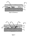
- a structure 1 which may be a microelectronic chip conventionally comprises at least one device 3, for example of the microelectronic type, arranged in a sealed cavity delimited by two substrates 2 and 4 and by a closed peripheral seal 5.
- the sealing of the cavity is ensured by the seal between the substrates and surrounding the device 3.
- the microelectronic device 3 is, for example, formed on the first substrate 2.
- the cavity is generally in depression with respect to the outside atmosphere, preferably under vacuum or under a controlled pressure of nitrogen or argon.
- the height of the cavity is defined by the height of the seal 5 surrounding the device 3 ( figure 1 ).
- the second substrate 4 may be structured so as to form a cover having a thinner central portion, so as to increase the volume of the cavity.
- the second substrate 4 is, for example, silicon, oxidized silicon or nitride or glass.
- the first substrate 2 is, for example, silicon or any other semiconductor material, with the exception of gallium arsenide (GaAs), or else another material on which a device already formed can be integrated.
- GaAs gallium arsenide
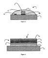
- the structure 1 comprises a closed and sealed cavity which is delimited by the substrate 3 and by an encapsulation layer 11.
- the tightness of the structure is then ensured by the adhesion between the encapsulation layer 11 and the substrate 2
- the encapsulation layer then acts as a closing cap as the substrate 4 of the figure 1 .
- the closure cap may have other layers in addition to the encapsulation layer.
- the height of the cavity is defined by the thickness of a sacrificial material 12 deposited on the substrate.
- the cavity comprises at least one getter 6, on at least one of its internal walls.
- the getter 6 is of multilayer type and comprises at least one adjustment sub-layer 8 located between one of the substrates 2 or 4 and a getter layer 7 which conventionally constitutes the adsorbent and / or absorbent layer.
- the getter layer 7 is, for example, a metal material chosen, preferably, so as to have a high nitrogen pumping capacity, this gas is commonly used during the encapsulation of the devices. If the getters 6 have, between them, different activation temperatures, it is advantageous to distinguish them for example in getters 6a and additional getters 6b ( Figures 3 and 4 ) or first 6a and second 6b getters.
- the getter 6 is formed on the substrate 2.
- An attachment sub-layer 9 is advantageously deposited on the substrate 2 before the adjustment sub-layer 8.
- the underlayer 9 is intended to allow better adhesion of the adjustment sub-layer 8 to the substrate 2.
- the underlayer 9 is typically made by any suitable technique, for example titanium or zirconium and has a thickness advantageously included between 20 and 100 nm.
- the adjustment sub-layer 8, located beneath and in contact with the getter layer 7, is intended to make it possible to modulate the activation temperature of the getter layer, that is to say to modulate the temperature at which the getter layer reacts with the atmosphere present inside the cavity.
- the adjustment sub-layer 8 is preferably Cu, Ni, Pt, Ag, Ru, Cr, Au, Al and has a thickness of preferably between 50 and 500 nm when the thickness of the getter layer 7a is of the order of several hundred nanometers, typically between 100 and 2000 nm.
- the thickness of the adjustment sub-layer can be reduced to a few tens of nanometers, typically between 10 and 90 nm, when the getter layer 7a is a few hundred nanometers, typically between 100 and 900 nm.
- an adjustment sub-layer 8 of 30 nm is sufficient for a getter layer 7a of 300 nm.
- the minimum thickness of the adjustment sub-layer 8 is approximately between 5% and 10% of the thickness of the getter layer 7a, for example equal to 8%.
- the adjustment sub-layer 8 is, for example, made of a metallic material, with the exception of palladium, deposited in the form of a pure body which, like platinum, for example, is chemically neutral vis-à-vis -vis the getter layer 7 in the desired activation domain.
- the adjustment sub-layer 8 may also be made of a material that becomes neutral or becomes a trap for certain chemical species, for example oxygen, after interaction with the getter layer 7.
- the adjustment sub-layer 8 may also be of a material which has a high chemical affinity for one or more chemical elements among carbon, oxygen and nitrogen.
- the underlayer may, for example, be chromium or aluminum. In the latter case, the aluminum underlayer 8 serves to protect the getter layer 7 when it is exposed to the ambient air, thus increasing the storage time of the getter without altering its properties, because the underlayment 8 avoids the growth of an oxide layer.
- This architecture is particularly advantageous for obtaining constant pumping capacities after exposure to ambient air for several months.
- Activation temperature a getter stack consisting of an aluminum adjustment sub-layer 8 and a titanium getter layer 7a is of the order of 400 ° C.
- a protective layer 10 may be disposed on the getter layer 7 to protect the getter.
- the getter 6 can maintain its pumping capacity after prolonged exposure to the ambient air or be protected from aggressive technological processes that could degrade it.
- a thin layer of chromium acting as a protective layer 10 can be used on the getter layer 7.
- thickness of the protective layer 10, for example chromium may be between 10 and 50nm, and preferably equal to 20nm.
- the addition of a protective layer 10 contributes to slightly increase the activation temperature of the getter, typically about twenty degrees Celsius for a layer of 20nm in Chrome.
- a regeneration pre-treatment can easily be implemented.
- the regeneration pretreatment consists in exposing the getter under a secondary vacuum, advantageously at a pressure of the order of 10 -7 mbar or under a partial pressure of a neutral gas not absorbed by the getter and at a temperature close to its activation temperature for a period that allows it to absorb the layer that degrades its pumping capacity.
- the getter is then cooled to room temperature, typically a temperature close to 20 ° C.
- the getter before it is exposed to ambient air, the getter is exposed to a known gas, preferably nitrogen, which is adsorb on the surface and thus temporarily protect the getter vis-à-vis the ambient air.
- a temperature of 350 ° C. is applied for a few hours to regenerate all the getters 6a described in the present invention.
- sacrificial getters deposited on the entire surface of a substrate.
- the sacrificial getter is chosen to have an activation temperature lower than that of the getter 6 (or getters 6a, 6b) which must be processed during the regeneration pre-treatment.
- the sacrificial getter is then used to improve the quality of the vacuum in the enclosure.
- the getters can thus be subjected to oxidizing atmospheres with which they react and then be regenerated as described above.
- these oxidizing atmospheres are generated during technological steps, in particular the steps of removing a sacrificial layer of polymer resin.
- the getter material 7 is subjected to such oxidizing atmospheres.
- the getter 6a and the device 3 are encapsulated by a sacrificial resin 12 and then by an encapsulation layer 11.
- the sacrificial resin is shaped, for example, by heating before the deposition of the encapsulation layer 11.
- the device and the getter are released from the sacrificial resin layer 12 from orifices made in the encapsulation layer 11.
- the sacrificial resin 12 may be a standard resin of positive polarity used in photolithography and or a resin of negative polarity of polyimide type. These resins can both be destroyed with a heat treatment in an oxidizing atmosphere. It is therefore particularly interesting to choose a getter 6 composed of at least one underlayer 8 and at least one getter layer 7 such that the activation temperature is greater than the baking temperature of the sacrificial resin. In this way, it avoids polluting the getter by the contaminants from the polymer and thus reduce or even cancel its pumping capacity.
- This embodiment is particularly advantageous for the manufacture of MEMS and Infra-Red detectors for burning the resin layers on which are built elements of the microdevice and its encapsulation layer.
- the getter materials are generally exposed to a generally oxidizing dry process in order to improve the propensity of the substrate on which the getter is deposited at the direct sealing. This treatment thus contributes to increasing the adhesion energy between the two substrates which delimit the cavity when they come into contact.
- a protective layer 10 made of chromium is then recommended.
- the choice of a getter 6a based activation temperature preferably less than 300 ° C, allows both to consolidate the seal and activate the getter at a temperature close to 400 ° C. Thus, the getter is activated during the consolidation consolidation treatment between the two substrates.
- the adjustment sub-layer 8 preferably has a coefficient of thermal expansion substantially between 5.10 -6 / ° C and 20.10 -6 / ° C, or even 23.10 -6 / ° C for aluminum and a ratio between its working temperature Te and its melting temperature Tf (in kelvin) substantially between 0.1 and 0.3.
- the activation temperature, of the associated getter layer 7, is then an increasing function of the expansion coefficient, the adjustment sub-layer 8 and the Te / Tf ratio and varies in a decreasing manner with the melting temperature of the Adjustment sub-layer 8. It is known that the coefficient of expansion of metals decreases when the melting temperature said metal increases.
- the deposition is carried out at a temperature close to room temperature on a silicon substrate.
- the effect of the adjustment sub-layer 8 on the getter layer 7 can be interpreted as follows.
- the getter effect in a metal material deposited in a thin layer occurs by diffusion of the adsorbed chemical species into the interior of the layer.
- the getter effect is therefore related to the microstructure, that is to say to the size, shape and orientation of the grains that make up the metallic material.
- Absorption of chemical species from the surface into the getter occurs by diffusion along the grain boundaries. This corresponds to a thermally activated phenomenon that occurs at relatively low temperature, compared to a diffusion of species in the grains.
- the structures most likely to have a getter effect are therefore those for which the grains are columnar and small, thus favoring diffusion at the grain boundaries.
- the structure of the deposit depends to a large extent on the ratio between the temperature of the substrate, that is to say the production temperature (Te), on which the metal is deposited and the melting temperature of the latter (Tf), the ratio Te / Tf (in degrees Kelvin).
- Te production temperature
- Tf melting temperature of the latter
- Te / Tf in degrees Kelvin.
- the diagrams of Movchan and Demchisin ( BA Movchan, AV Demchishin, 1969, Phys. Met. Metallogr., 28, p.83 ) and Thornton ( JA Thornton, 1986, J. Vac. Sci. Technol., A4 (6), p.3059 ) on the other hand provide a map prediction of the microstructure as a function of the Te / Tf ratio and the pressure.
- a ruthenium underlayer 8 could by its microstructure ( preferential germination of the getter layer 7 at grain boundaries, triple knots or between the domes of the underlying structure) and / or its high melting temperature limit the surface migration of the getter metal and thus lead to a structure of this ci thinner than in the opposite case or the getter layer 7 is deposited on aluminum.
- the same adjustment sub-layer 8 to modulate the activation temperature Ta of the getter layer 7. It suffices to adjust the microstructure of the adjustment sub-layer 8 by according to its production temperature Te, while remaining in a temperature range which will allow to give the adjustment sub-layer a sufficiently fine structure for the getter to be activated by a diffusion method mainly at the grain boundaries .
- the getters 6 can be divided into at least getters 6a and additional getters 6b.
- the getter comprises a getter layer 7 constituted by at least two elementary layers 7a and 7b. Such an example does not form part of the present invention.
- the adjustment sub-layer of the getter 6a has, for example, a grain structure greater than the portion of the adjustment sub-layer of the additional getter 6b.
- the grains of the adjustment sub-layer 8 of the getter 6a are larger than the grains of the adjustment sub-layer 8 of the additional getter 6b.
- the adjustment sub-layer 8 being located between the getter layer and the substrate 2, it also makes it possible to eliminate the chemical interactions between the substrate 2 and the getter layer 7. Thus, the pumping capacity of the getter layer 7 is preserved.
- the getter layer 7 deposited on the adjustment sub-layer 8 is made of Ti or Zr and has a thickness of between 100 and 2000 nm.
- the activation temperature of the getter layer, without the action of the adjustment sub-layer 8, is greater than 425 ° C. and close to 450 ° C. With the action of the adjustment sub-layer 8, the activation temperature of the getter layer 7 varies according to the nature of this adjustment sub-layer 8.
- the activation temperature of the getter layer 7, in titanium or zirconium, can vary increasingly substantially between 275 and 425 ° C according to the adjustment sub-layer 8.
- Table 1 gives, by way of example, a few values of activation temperature of a getter 6 according to the nature of its adjustment sub-layer 8, for a getter layer 7 made of titanium. All the deposits are produced by evaporation on a silicon substrate at an identical elaboration temperature Te, close to the ambient temperature. Nature of the adjustment sub-layer 8 Activation temperature Ru 275 ° C Cr 300 ° C Pt 325 ° C Or 350 ° C At 365 ° C Cu 375 ° C Ag 380 ° C al 400 ° C
- the microstructure of the zirconium deposit must be finer than that of titanium.
- the activation temperatures presented in Table 1 should therefore be substantially lower with a zirconium getter sublayer than with a titanium getter layer.
- the getter layer 7 is according to the invention constituted by the stacking of a plurality of elementary getter layers, preferably two, 7a, 7b, of different chemical compositions.
- the elementary getter layers are deposited one above the other on the adjustment sub-layer 8.
- the first elementary getter layer 7a, in contact with the the adjustment sub-layer 8 has an activation temperature greater than that of the second elementary getter layer 7b which covers it.
- the elementary getter layers 7a, 7b have a decreasing activation temperature as they move away from the underlayer 8.
- the first elementary getter layer 7a in contact with the adjustment sub-layer 8, is preferably of titanium and has a thickness of preferably between 100 and 1000 nm.
- the use of two different elementary getter layers 7a, 7b is particularly advantageous for repackaging the chip during its lifetime by activation of the first layer 7a.
- the adjustment sub-layer 8 of the multilayer getter may be chosen so as to increase the reflectivity of the getter to infrared radiation, typically when the getter is chosen to be reflective to infrared radiation (for certain specific applications).
- This reflective function is advantageously chosen, depending in particular on the nature of the material of the adjustment sub-layer 8 which is advantageously made of copper or aluminum. For example, in a bolometer, this reflectivity is sufficient to place the getter as an IR reflector.
- the getter 6 has another essential function: IR reflector. If the layer is made of titanium, it already has some reflectivity to infrared radiation. The use of an undercoat adapted adjustment then makes it possible to increase the reflectivity to the infrared radiation to the entire getter.
- the multilayer getter 6 comprising at least the adjustment sub-layer 8, the getter layer 7 and possibly the underlayer 9 can be made anywhere in the cavity and for example on the substrate 2 or 4 before or after formation of the microelectronic device 3. Such a getter 6 can also be formed on the two substrates 2 and 4 delimiting the cavity.
- the anchoring sub-layer 9 is advantageously deposited by any suitable technique, preferably by evaporation on the substrate 2.
- the adjustment sub-layer 8 and then the first and second elementary getter layers (7a, 7b) are then deposited successively. , advantageously by evaporation, on the attachment sub-layer 9.
- the deposits of the different layers are made within the same deposition equipment.
- the attachment sub-layer 9 can contribute to improving the quality of the vacuum in this deposition chamber, when the material forming this layer (for example Ti or Zr) has getter properties.
- the getter 6 can be structured in a conventional manner, for example by lithography and dry etching, advantageously by a non-reactive plasma and / or wet, so as to precisely locate the areas in which the getter layers 7 are desired.
- the adhesion of the positive resin used for the lithography on the getter layer 7 can be improved, if necessary, by providing an adhesion promoter, advantageously hexamethyldisilazane (HDMS).
- HDMS hexamethyldisilazane
- the layers 7, 8, 9 and 10 are etched from usual liquid chemical reagents and / or by a neutral plasma depending on the materials used.
- a neutral plasma depending on the materials used.
- the two etching modes can also be used when there is incompatibility between the etching reagents of the different layers. This incompatibility can lead to phenomena of over-etching or even alteration of certain layers.
- the step of removing the positive resin and optionally all or part of the promoter may be performed by a conventional product used in the microelectronics industry and advantageously followed by cleaning with fuming nitric acid, when the latter does not affect the underlayer 8. Finally, a dry etching with a non-reactive plasma allows, if necessary, to eliminate pollutants or residues from previous technological steps and present on the surface of the getter layer 7.
- the getter can also be structured during the deposit by a lift-off process.
- a photosensitive dry film of negative polarity is laminated to the substrate.
- the dry film having a thickness of between 5 and 50 ⁇ m, advantageously equal to 15 ⁇ m, is insulated and developed according to a conventional photolithography step.
- the assembly is then subjected to secondary vacuum treatment to remove development residues.
- the deposition of the getter is then carried out, for example, by spraying, advantageously by evaporation.
- the removal of the unexposed dry film is carried out by means of a specific product, which does not modify the properties of the getter material.
- the production methods described above it is possible to successively produce several getters 6, having different activation temperatures on the same substrate and / or in the same cavity.
- the structuring of the getter 6 is performed by chemical etching, it is advantageous to deposit and structure the different sub-layers 8 adjustment of different getters.
- the getter layer 7 is then deposited and then structured by chemical etching. Since the adjustment layer 8 and the getter layer 7 are not made immediately afterwards and in the same equipment, it is preferable to use a regeneration pretreatment as described above.
- the structuring of the getter 6 is performed by detachment, it is possible to make successive deposits of getters 6, by rolling a dry film on a getter already formed. It is then possible to adjust, in the same structure, the activation temperature of several different getters.
- the pumping capacity of each getter in terms of the number of moles adsorbed or absorbed can be controlled, which makes it possible to modulate the pressure inside the cavity that contains the getters.
Landscapes
- Engineering & Computer Science (AREA)
- Microelectronics & Electronic Packaging (AREA)
- Computer Hardware Design (AREA)
- Physics & Mathematics (AREA)
- Condensed Matter Physics & Semiconductors (AREA)
- General Physics & Mathematics (AREA)
- Power Engineering (AREA)
- Micromachines (AREA)
- Manufacture Of Electron Tubes, Discharge Lamp Vessels, Lead-In Wires, And The Like (AREA)
- Common Detailed Techniques For Electron Tubes Or Discharge Tubes (AREA)
- Solid-Sorbent Or Filter-Aiding Compositions (AREA)
- Bipolar Transistors (AREA)
Priority Applications (1)
| Application Number | Priority Date | Filing Date | Title |
|---|---|---|---|
| EP10158202.1A EP2204347B1 (fr) | 2007-10-15 | 2008-10-09 | Structure comportant une couche getter et une sous-couche d'ajustement de la température d'activation et procédé de fabrication |
Applications Claiming Priority (2)
| Application Number | Priority Date | Filing Date | Title |
|---|---|---|---|
| FR0707212A FR2922202B1 (fr) | 2007-10-15 | 2007-10-15 | Structure comportant une couche getter et une sous-couche d'ajustement et procede de fabrication. |
| PCT/FR2008/001420 WO2009087284A1 (fr) | 2007-10-15 | 2008-10-09 | Structure comportant une couche getter et une sous-couche d'ajustement et procédé de fabrication |
Related Child Applications (2)
| Application Number | Title | Priority Date | Filing Date |
|---|---|---|---|
| EP10158202.1A Division EP2204347B1 (fr) | 2007-10-15 | 2008-10-09 | Structure comportant une couche getter et une sous-couche d'ajustement de la température d'activation et procédé de fabrication |
| EP10158202.1 Division-Into | 2010-03-29 |
Publications (2)
| Publication Number | Publication Date |
|---|---|
| EP2197780A1 EP2197780A1 (fr) | 2010-06-23 |
| EP2197780B1 true EP2197780B1 (fr) | 2011-02-02 |
Family
ID=39462016
Family Applications (2)
| Application Number | Title | Priority Date | Filing Date |
|---|---|---|---|
| EP08869876A Active EP2197780B1 (fr) | 2007-10-15 | 2008-10-09 | Structure comportant une couche getter et une sous-couche d'ajustement et procédé de fabrication |
| EP10158202.1A Active EP2204347B1 (fr) | 2007-10-15 | 2008-10-09 | Structure comportant une couche getter et une sous-couche d'ajustement de la température d'activation et procédé de fabrication |
Family Applications After (1)
| Application Number | Title | Priority Date | Filing Date |
|---|---|---|---|
| EP10158202.1A Active EP2204347B1 (fr) | 2007-10-15 | 2008-10-09 | Structure comportant une couche getter et une sous-couche d'ajustement de la température d'activation et procédé de fabrication |
Country Status (8)
| Country | Link |
|---|---|
| US (2) | US8605445B2 (enExample) |
| EP (2) | EP2197780B1 (enExample) |
| JP (1) | JP5431343B2 (enExample) |
| AT (1) | ATE497481T1 (enExample) |
| CA (1) | CA2701363A1 (enExample) |
| DE (1) | DE602008004848D1 (enExample) |
| FR (1) | FR2922202B1 (enExample) |
| WO (1) | WO2009087284A1 (enExample) |
Cited By (2)
| Publication number | Priority date | Publication date | Assignee | Title |
|---|---|---|---|---|
| EP2581338A1 (fr) | 2011-10-11 | 2013-04-17 | Commissariat à l'Énergie Atomique et aux Énergies Alternatives | Procédé d'encapsulation de micro-dispositif par report de capot et depot de getter à travers le capot |
| EP2884529A1 (fr) | 2013-11-29 | 2015-06-17 | Commissariat à l'Énergie Atomique et aux Énergies Alternatives | Procédé de réalisation d'un substrat comportant un matériau getter disposé sur des parois d'un ou plusieurs trous borgnes formés dans le substrat |
Families Citing this family (30)
| Publication number | Priority date | Publication date | Assignee | Title |
|---|---|---|---|---|
| JP3271272B2 (ja) | 1991-11-12 | 2002-04-02 | 日本電気株式会社 | 半導体装置の製造方法 |
| FR2950876B1 (fr) | 2009-10-07 | 2012-02-10 | Commissariat Energie Atomique | Procede de traitement d'un materiau getter et procede d'encapsulation d'un tel materiau getter |
| FR2950877B1 (fr) | 2009-10-07 | 2012-01-13 | Commissariat Energie Atomique | Structure a cavite comportant une interface de collage a base de materiau getter |
| FR2952627A1 (fr) * | 2009-11-17 | 2011-05-20 | Commissariat Energie Atomique | Getter ayant deux temperatures d'activation et structure comportant ce getter |
| EP2363373A1 (en) * | 2010-03-02 | 2011-09-07 | SensoNor Technologies AS | Bonding process for sensitive micro-and nano-systems |
| FR2967302B1 (fr) * | 2010-11-09 | 2012-12-21 | Commissariat Energie Atomique | Structure d'encapsulation d'un micro-dispositif comportant un matériau getter |
| FR2967150A1 (fr) * | 2010-11-09 | 2012-05-11 | Commissariat Energie Atomique | Procédé de réalisation de substrat a couches enfouies de matériau getter |
| FR2976932A1 (fr) * | 2011-06-23 | 2012-12-28 | Commissariat Energie Atomique | Structure a materiau getter protege hermetiquement lors de sa realisation |
| FR2977883B1 (fr) | 2011-07-11 | 2014-03-14 | Commissariat Energie Atomique | Structure getter a capacite de pompage optimisee |
| FR2981198B1 (fr) | 2011-10-11 | 2014-04-04 | Commissariat Energie Atomique | Structure d'encapsulation de dispositif electronique et procede de realisation d'une telle structure |
| FR2982073B1 (fr) * | 2011-10-28 | 2014-10-10 | Commissariat Energie Atomique | Structure d'encapsulation hermetique d'un dispositif et d'un composant electronique |
| US9240362B2 (en) | 2012-06-20 | 2016-01-19 | Agency For Science, Technology And Research | Layer arrangement and a wafer level package comprising the layer arrangement |
| JP6230286B2 (ja) * | 2012-08-20 | 2017-11-15 | セイコーインスツル株式会社 | 電子デバイス及び電子デバイスの製造方法 |
| JP6230285B2 (ja) * | 2012-08-24 | 2017-11-15 | セイコーインスツル株式会社 | 電子デバイス、memsセンサ及び電子デバイスの製造方法 |
| CN103140026B (zh) * | 2013-02-04 | 2015-12-02 | 深圳市佳捷特陶瓷电路技术有限公司 | 陶瓷覆铜板及其制备方法 |
| EP2813465B1 (en) * | 2013-06-12 | 2020-01-15 | Tronic's Microsystems | MEMS device with getter layer |
| FR3008965B1 (fr) | 2013-07-26 | 2017-03-03 | Commissariat Energie Atomique | Structure d'encapsulation comprenant un capot renforce mecaniquement et a effet getter |
| US9637378B2 (en) | 2013-09-11 | 2017-05-02 | Taiwan Semiconductor Manufacturing Co., Ltd. | Cup-like getter scheme |
| US9242853B2 (en) | 2013-10-15 | 2016-01-26 | Taiwan Semiconductor Manufacturing Co., Ltd. | Method of improving getter efficiency by increasing superficial area |
| FR3014241B1 (fr) | 2013-11-29 | 2017-05-05 | Commissariat Energie Atomique | Structure d'encapsulation comprenant des tranchees partiellement remplies de materiau getter |
| FR3030475B1 (fr) | 2014-12-17 | 2017-01-20 | Commissariat Energie Atomique | Structure getter multi-niveaux et structure d'encapsulation comportant une telle structure getter multi-niveaux |
| US9718672B2 (en) | 2015-05-27 | 2017-08-01 | Globalfoundries Singapore Pte. Ltd. | Electronic devices including substantially hermetically sealed cavities and getter films with Kelvin measurement arrangement for evaluating the getter films and methods for fabricating the same |
| US9438411B1 (en) | 2015-08-12 | 2016-09-06 | The Boeing Company | Method and apparatus for synchronizing digital messages |
| US9570321B1 (en) * | 2015-10-20 | 2017-02-14 | Raytheon Company | Use of an external getter to reduce package pressure |
| JP2018054496A (ja) * | 2016-09-29 | 2018-04-05 | セイコーインスツル株式会社 | パッケージおよび赤外線センサ |
| FR3072788B1 (fr) | 2017-10-24 | 2020-05-29 | Commissariat A L'energie Atomique Et Aux Energies Alternatives | Source de rayonnement infrarouge modulable |
| CN108249386B (zh) * | 2018-01-23 | 2020-09-08 | 苏州大学 | 激活温度可控的非蒸散型薄膜吸气剂及其应用 |
| US10526199B1 (en) * | 2018-09-27 | 2020-01-07 | Taiwan Semiconductor Manufacturing Co., Ltd. | High efficiency getter design in vacuum MEMS device |
| JP2021136413A (ja) * | 2020-02-28 | 2021-09-13 | 国立研究開発法人産業技術総合研究所 | 封止構造体およびその製造方法 |
| CN111892014B (zh) * | 2020-07-30 | 2023-10-31 | 钢铁研究总院 | 一种吸气薄膜及其制备方法 |
Family Cites Families (20)
| Publication number | Priority date | Publication date | Assignee | Title |
|---|---|---|---|---|
| US4127134A (en) * | 1977-04-11 | 1978-11-28 | Cordis Corporation | Gas-absorbing pacer and method of fabrication |
| US4302498A (en) * | 1980-10-28 | 1981-11-24 | Rca Corporation | Laminated conducting film on an integrated circuit substrate and method of forming the laminate |
| US4814945A (en) * | 1987-09-18 | 1989-03-21 | Trw Inc. | Multilayer printed circuit board for ceramic chip carriers |
| US5577020A (en) * | 1993-10-08 | 1996-11-19 | Tdk Corporation | Magneto-optical disc with intermediate film layer between a recording film and a dielectric film |
| US5456740A (en) * | 1994-06-22 | 1995-10-10 | Millipore Corporation | High-efficiency metal membrane getter element and process for making |
| TW355845B (en) * | 1995-03-27 | 1999-04-11 | Semiconductor Energy Lab Co Ltd | Semiconductor device and a method of manufacturing the same |
| US5943601A (en) * | 1997-04-30 | 1999-08-24 | International Business Machines Corporation | Process for fabricating a metallization structure |
| US5866978A (en) * | 1997-09-30 | 1999-02-02 | Fed Corporation | Matrix getter for residual gas in vacuum sealed panels |
| US6110808A (en) * | 1998-12-04 | 2000-08-29 | Trw Inc. | Hydrogen getter for integrated microelectronic assembly |
| US6423575B1 (en) * | 2001-07-27 | 2002-07-23 | Dean Tran | Hydrogen gettering structure including silver-doped palladium layer to increase hydrogen gettering of module component and semiconductor device module having such structure, and methods of fabrication |
| US20030062610A1 (en) * | 2001-09-28 | 2003-04-03 | Kovacs Alan L. | Multilayer thin film hydrogen getter |
| US6923625B2 (en) * | 2002-01-07 | 2005-08-02 | Integrated Sensing Systems, Inc. | Method of forming a reactive material and article formed thereby |
| JP2004066225A (ja) * | 2002-06-13 | 2004-03-04 | Lg Electronics Inc | ゲッタの組成物及び該ゲッタの組成物を利用した電界放出表示装置 |
| US6806557B2 (en) * | 2002-09-30 | 2004-10-19 | Motorola, Inc. | Hermetically sealed microdevices having a single crystalline silicon getter for maintaining vacuum |
| US6988924B2 (en) * | 2003-04-14 | 2006-01-24 | Hewlett-Packard Development Company, L.P. | Method of making a getter structure |
| ITMI20031178A1 (it) * | 2003-06-11 | 2004-12-12 | Getters Spa | Depositi multistrato getter non evaporabili ottenuti per |
| ITMI20032209A1 (it) * | 2003-11-14 | 2005-05-15 | Getters Spa | Processo per la produzione di dispositivi che richiedono per il loro funzionamento un materiale getter non evaporabile. |
| US20060230927A1 (en) * | 2005-04-02 | 2006-10-19 | Xiaobing Xie | Hydrogen separation |
| ITMI20050616A1 (it) * | 2005-04-12 | 2006-10-13 | Getters Spa | Processo per la formazione di depositi getter miniaturizzati e depositi getrter cosi'ottenuti |
| ITMI20052343A1 (it) * | 2005-12-06 | 2007-06-07 | Getters Spa | Processo per la produzione di dispositivi micromeccanici contenenti un materiale getter e dispositivi cosi'prodotti |
-
2007
- 2007-10-15 FR FR0707212A patent/FR2922202B1/fr not_active Expired - Fee Related
-
2008
- 2008-10-09 US US12/679,487 patent/US8605445B2/en active Active
- 2008-10-09 EP EP08869876A patent/EP2197780B1/fr active Active
- 2008-10-09 EP EP10158202.1A patent/EP2204347B1/fr active Active
- 2008-10-09 AT AT08869876T patent/ATE497481T1/de not_active IP Right Cessation
- 2008-10-09 JP JP2010529422A patent/JP5431343B2/ja active Active
- 2008-10-09 DE DE602008004848T patent/DE602008004848D1/de active Active
- 2008-10-09 CA CA2701363A patent/CA2701363A1/fr not_active Abandoned
- 2008-10-09 WO PCT/FR2008/001420 patent/WO2009087284A1/fr not_active Ceased
-
2010
- 2010-03-23 US US12/729,634 patent/US8414963B2/en active Active
Cited By (4)
| Publication number | Priority date | Publication date | Assignee | Title |
|---|---|---|---|---|
| EP2581338A1 (fr) | 2011-10-11 | 2013-04-17 | Commissariat à l'Énergie Atomique et aux Énergies Alternatives | Procédé d'encapsulation de micro-dispositif par report de capot et depot de getter à travers le capot |
| US8999762B2 (en) | 2011-10-11 | 2015-04-07 | Commissariat à l'énergie atomique et aux énergies alternatives | Process for encapsulating a micro-device by attaching a cap and depositing getter through the cap |
| EP2884529A1 (fr) | 2013-11-29 | 2015-06-17 | Commissariat à l'Énergie Atomique et aux Énergies Alternatives | Procédé de réalisation d'un substrat comportant un matériau getter disposé sur des parois d'un ou plusieurs trous borgnes formés dans le substrat |
| US9277656B2 (en) | 2013-11-29 | 2016-03-01 | Comissariat a l'énergie atomique et aux énergies alternatives | Method to fabricate a substrate including a material disposed on the edge of one or more non through hole formed in the substrate |
Also Published As
| Publication number | Publication date |
|---|---|
| WO2009087284A1 (fr) | 2009-07-16 |
| EP2204347A1 (fr) | 2010-07-07 |
| EP2197780A1 (fr) | 2010-06-23 |
| US8414963B2 (en) | 2013-04-09 |
| EP2204347B1 (fr) | 2016-03-30 |
| ATE497481T1 (de) | 2011-02-15 |
| FR2922202B1 (fr) | 2009-11-20 |
| US20100193215A1 (en) | 2010-08-05 |
| US8605445B2 (en) | 2013-12-10 |
| FR2922202A1 (fr) | 2009-04-17 |
| DE602008004848D1 (de) | 2011-03-17 |
| CA2701363A1 (fr) | 2009-07-16 |
| JP2011501426A (ja) | 2011-01-06 |
| US20100178419A1 (en) | 2010-07-15 |
| JP5431343B2 (ja) | 2014-03-05 |
Similar Documents
| Publication | Publication Date | Title |
|---|---|---|
| EP2197780B1 (fr) | Structure comportant une couche getter et une sous-couche d'ajustement et procédé de fabrication | |
| EP2308798B1 (fr) | Procédé de traitement d'un matériau getter et procédé d'encapsulation d'un tel matériau getter | |
| EP2322469B1 (fr) | Getter ayant deux températures d'activation et structure comportant ce getter | |
| EP2308797B1 (fr) | Structure à cavité comportant une interface de collage à base de matériau getter | |
| EP2141117B1 (fr) | Procédé d'encapsulation d'un dispositif microélectronique par un materiau getter | |
| EP2450949B1 (fr) | Structure d'encapsulation d'un micro-dispositif comportant un matériau getter | |
| EP2637966B1 (fr) | Procede de realisation de substrat a couches enfouies de materiau getter | |
| EP1878693B1 (fr) | Microcomposant encapsule equipe d'au moins un getter | |
| FR2883099A1 (fr) | Protection d'un getter en couche mince | |
| EP2537797B1 (fr) | Structure à matériau getter protégée hermétiquement lors de sa réalisation | |
| EP3034460B1 (fr) | Structure getter multi-niveaux et structure d'encapsulation comportant une telle structure getter multi-niveaux | |
| EP2537796B1 (fr) | Structure getter comportant un matériau perméable aux gaz | |
| FR3053046A1 (fr) | Procede de collage reversible entre deux elements | |
| WO2020008125A1 (fr) | Boitier hermetique comportant un getter, composant integrant un tel boitier hermetique et procede de fabrication associe | |
| FR2865946A1 (fr) | Procede de realisation d'une couche de materiau sur un support |
Legal Events
| Date | Code | Title | Description |
|---|---|---|---|
| PUAI | Public reference made under article 153(3) epc to a published international application that has entered the european phase |
Free format text: ORIGINAL CODE: 0009012 |
|
| 17P | Request for examination filed |
Effective date: 20100315 |
|
| AK | Designated contracting states |
Kind code of ref document: A1 Designated state(s): AT BE BG CH CY CZ DE DK EE ES FI FR GB GR HR HU IE IS IT LI LT LU LV MC MT NL NO PL PT RO SE SI SK TR |
|
| AX | Request for extension of the european patent |
Extension state: AL BA MK RS |
|
| GRAP | Despatch of communication of intention to grant a patent |
Free format text: ORIGINAL CODE: EPIDOSNIGR1 |
|
| RTI1 | Title (correction) |
Free format text: STRUCTURE COMPRISING A GETTER LAYER AND AN ADJUSTMENT SUBLAYER, AND FABRICATION PROCESS |
|
| GRAS | Grant fee paid |
Free format text: ORIGINAL CODE: EPIDOSNIGR3 |
|
| GRAA | (expected) grant |
Free format text: ORIGINAL CODE: 0009210 |
|
| DAX | Request for extension of the european patent (deleted) | ||
| AK | Designated contracting states |
Kind code of ref document: B1 Designated state(s): AT BE BG CH CY CZ DE DK EE ES FI FR GB GR HR HU IE IS IT LI LT LU LV MC MT NL NO PL PT RO SE SI SK TR |
|
| REG | Reference to a national code |
Ref country code: GB Ref legal event code: FG4D Free format text: NOT ENGLISH |
|
| REG | Reference to a national code |
Ref country code: CH Ref legal event code: EP |
|
| REG | Reference to a national code |
Ref country code: IE Ref legal event code: FG4D Free format text: LANGUAGE OF EP DOCUMENT: FRENCH |
|
| REF | Corresponds to: |
Ref document number: 602008004848 Country of ref document: DE Date of ref document: 20110317 Kind code of ref document: P |
|
| REG | Reference to a national code |
Ref country code: DE Ref legal event code: R096 Ref document number: 602008004848 Country of ref document: DE Effective date: 20110317 |
|
| REG | Reference to a national code |
Ref country code: NL Ref legal event code: VDEP Effective date: 20110202 |
|
| LTIE | Lt: invalidation of european patent or patent extension |
Effective date: 20110202 |
|
| PG25 | Lapsed in a contracting state [announced via postgrant information from national office to epo] |
Ref country code: PT Free format text: LAPSE BECAUSE OF FAILURE TO SUBMIT A TRANSLATION OF THE DESCRIPTION OR TO PAY THE FEE WITHIN THE PRESCRIBED TIME-LIMIT Effective date: 20110602 Ref country code: IS Free format text: LAPSE BECAUSE OF FAILURE TO SUBMIT A TRANSLATION OF THE DESCRIPTION OR TO PAY THE FEE WITHIN THE PRESCRIBED TIME-LIMIT Effective date: 20110602 Ref country code: SE Free format text: LAPSE BECAUSE OF FAILURE TO SUBMIT A TRANSLATION OF THE DESCRIPTION OR TO PAY THE FEE WITHIN THE PRESCRIBED TIME-LIMIT Effective date: 20110202 Ref country code: LV Free format text: LAPSE BECAUSE OF FAILURE TO SUBMIT A TRANSLATION OF THE DESCRIPTION OR TO PAY THE FEE WITHIN THE PRESCRIBED TIME-LIMIT Effective date: 20110202 Ref country code: ES Free format text: LAPSE BECAUSE OF FAILURE TO SUBMIT A TRANSLATION OF THE DESCRIPTION OR TO PAY THE FEE WITHIN THE PRESCRIBED TIME-LIMIT Effective date: 20110513 Ref country code: HR Free format text: LAPSE BECAUSE OF FAILURE TO SUBMIT A TRANSLATION OF THE DESCRIPTION OR TO PAY THE FEE WITHIN THE PRESCRIBED TIME-LIMIT Effective date: 20110202 Ref country code: GR Free format text: LAPSE BECAUSE OF FAILURE TO SUBMIT A TRANSLATION OF THE DESCRIPTION OR TO PAY THE FEE WITHIN THE PRESCRIBED TIME-LIMIT Effective date: 20110503 Ref country code: LT Free format text: LAPSE BECAUSE OF FAILURE TO SUBMIT A TRANSLATION OF THE DESCRIPTION OR TO PAY THE FEE WITHIN THE PRESCRIBED TIME-LIMIT Effective date: 20110202 Ref country code: NO Free format text: LAPSE BECAUSE OF FAILURE TO SUBMIT A TRANSLATION OF THE DESCRIPTION OR TO PAY THE FEE WITHIN THE PRESCRIBED TIME-LIMIT Effective date: 20110502 |
|
| PG25 | Lapsed in a contracting state [announced via postgrant information from national office to epo] |
Ref country code: NL Free format text: LAPSE BECAUSE OF FAILURE TO SUBMIT A TRANSLATION OF THE DESCRIPTION OR TO PAY THE FEE WITHIN THE PRESCRIBED TIME-LIMIT Effective date: 20110202 Ref country code: PL Free format text: LAPSE BECAUSE OF FAILURE TO SUBMIT A TRANSLATION OF THE DESCRIPTION OR TO PAY THE FEE WITHIN THE PRESCRIBED TIME-LIMIT Effective date: 20110202 Ref country code: SI Free format text: LAPSE BECAUSE OF FAILURE TO SUBMIT A TRANSLATION OF THE DESCRIPTION OR TO PAY THE FEE WITHIN THE PRESCRIBED TIME-LIMIT Effective date: 20110202 Ref country code: AT Free format text: LAPSE BECAUSE OF FAILURE TO SUBMIT A TRANSLATION OF THE DESCRIPTION OR TO PAY THE FEE WITHIN THE PRESCRIBED TIME-LIMIT Effective date: 20110202 Ref country code: FI Free format text: LAPSE BECAUSE OF FAILURE TO SUBMIT A TRANSLATION OF THE DESCRIPTION OR TO PAY THE FEE WITHIN THE PRESCRIBED TIME-LIMIT Effective date: 20110202 Ref country code: BG Free format text: LAPSE BECAUSE OF FAILURE TO SUBMIT A TRANSLATION OF THE DESCRIPTION OR TO PAY THE FEE WITHIN THE PRESCRIBED TIME-LIMIT Effective date: 20110502 Ref country code: CY Free format text: LAPSE BECAUSE OF FAILURE TO SUBMIT A TRANSLATION OF THE DESCRIPTION OR TO PAY THE FEE WITHIN THE PRESCRIBED TIME-LIMIT Effective date: 20110202 |
|
| REG | Reference to a national code |
Ref country code: IE Ref legal event code: FD4D |
|
| PG25 | Lapsed in a contracting state [announced via postgrant information from national office to epo] |
Ref country code: EE Free format text: LAPSE BECAUSE OF FAILURE TO SUBMIT A TRANSLATION OF THE DESCRIPTION OR TO PAY THE FEE WITHIN THE PRESCRIBED TIME-LIMIT Effective date: 20110202 Ref country code: DK Free format text: LAPSE BECAUSE OF FAILURE TO SUBMIT A TRANSLATION OF THE DESCRIPTION OR TO PAY THE FEE WITHIN THE PRESCRIBED TIME-LIMIT Effective date: 20110202 Ref country code: IE Free format text: LAPSE BECAUSE OF FAILURE TO SUBMIT A TRANSLATION OF THE DESCRIPTION OR TO PAY THE FEE WITHIN THE PRESCRIBED TIME-LIMIT Effective date: 20110202 |
|
| PG25 | Lapsed in a contracting state [announced via postgrant information from national office to epo] |
Ref country code: CZ Free format text: LAPSE BECAUSE OF FAILURE TO SUBMIT A TRANSLATION OF THE DESCRIPTION OR TO PAY THE FEE WITHIN THE PRESCRIBED TIME-LIMIT Effective date: 20110202 Ref country code: RO Free format text: LAPSE BECAUSE OF FAILURE TO SUBMIT A TRANSLATION OF THE DESCRIPTION OR TO PAY THE FEE WITHIN THE PRESCRIBED TIME-LIMIT Effective date: 20110202 Ref country code: SK Free format text: LAPSE BECAUSE OF FAILURE TO SUBMIT A TRANSLATION OF THE DESCRIPTION OR TO PAY THE FEE WITHIN THE PRESCRIBED TIME-LIMIT Effective date: 20110202 |
|
| PLBE | No opposition filed within time limit |
Free format text: ORIGINAL CODE: 0009261 |
|
| STAA | Information on the status of an ep patent application or granted ep patent |
Free format text: STATUS: NO OPPOSITION FILED WITHIN TIME LIMIT |
|
| 26N | No opposition filed |
Effective date: 20111103 |
|
| REG | Reference to a national code |
Ref country code: DE Ref legal event code: R097 Ref document number: 602008004848 Country of ref document: DE Effective date: 20111103 |
|
| BERE | Be: lapsed |
Owner name: COMMISSARIAT A L'ENERGIE ATOMIQUE ET AUX ENERGIES Effective date: 20111031 |
|
| PG25 | Lapsed in a contracting state [announced via postgrant information from national office to epo] |
Ref country code: MC Free format text: LAPSE BECAUSE OF NON-PAYMENT OF DUE FEES Effective date: 20111031 |
|
| PG25 | Lapsed in a contracting state [announced via postgrant information from national office to epo] |
Ref country code: BE Free format text: LAPSE BECAUSE OF NON-PAYMENT OF DUE FEES Effective date: 20111031 |
|
| PG25 | Lapsed in a contracting state [announced via postgrant information from national office to epo] |
Ref country code: MT Free format text: LAPSE BECAUSE OF FAILURE TO SUBMIT A TRANSLATION OF THE DESCRIPTION OR TO PAY THE FEE WITHIN THE PRESCRIBED TIME-LIMIT Effective date: 20110202 |
|
| PG25 | Lapsed in a contracting state [announced via postgrant information from national office to epo] |
Ref country code: LU Free format text: LAPSE BECAUSE OF NON-PAYMENT OF DUE FEES Effective date: 20111009 |
|
| REG | Reference to a national code |
Ref country code: CH Ref legal event code: PL |
|
| PG25 | Lapsed in a contracting state [announced via postgrant information from national office to epo] |
Ref country code: CH Free format text: LAPSE BECAUSE OF NON-PAYMENT OF DUE FEES Effective date: 20121031 Ref country code: LI Free format text: LAPSE BECAUSE OF NON-PAYMENT OF DUE FEES Effective date: 20121031 |
|
| PG25 | Lapsed in a contracting state [announced via postgrant information from national office to epo] |
Ref country code: TR Free format text: LAPSE BECAUSE OF FAILURE TO SUBMIT A TRANSLATION OF THE DESCRIPTION OR TO PAY THE FEE WITHIN THE PRESCRIBED TIME-LIMIT Effective date: 20110202 |
|
| PG25 | Lapsed in a contracting state [announced via postgrant information from national office to epo] |
Ref country code: HU Free format text: LAPSE BECAUSE OF FAILURE TO SUBMIT A TRANSLATION OF THE DESCRIPTION OR TO PAY THE FEE WITHIN THE PRESCRIBED TIME-LIMIT Effective date: 20110202 |
|
| REG | Reference to a national code |
Ref country code: FR Ref legal event code: PLFP Year of fee payment: 8 |
|
| REG | Reference to a national code |
Ref country code: FR Ref legal event code: PLFP Year of fee payment: 9 |
|
| REG | Reference to a national code |
Ref country code: FR Ref legal event code: PLFP Year of fee payment: 10 |
|
| REG | Reference to a national code |
Ref country code: FR Ref legal event code: PLFP Year of fee payment: 11 |
|
| P01 | Opt-out of the competence of the unified patent court (upc) registered |
Effective date: 20230830 |
|
| PGFP | Annual fee paid to national office [announced via postgrant information from national office to epo] |
Ref country code: DE Payment date: 20241022 Year of fee payment: 17 |
|
| PGFP | Annual fee paid to national office [announced via postgrant information from national office to epo] |
Ref country code: GB Payment date: 20241024 Year of fee payment: 17 |
|
| PGFP | Annual fee paid to national office [announced via postgrant information from national office to epo] |
Ref country code: FR Payment date: 20241024 Year of fee payment: 17 |
|
| PGFP | Annual fee paid to national office [announced via postgrant information from national office to epo] |
Ref country code: IT Payment date: 20241031 Year of fee payment: 17 |